EP2202326A1 - Blechmaterial aus kupferlegierung für elektrische und elektronische bauteile - Google Patents
Blechmaterial aus kupferlegierung für elektrische und elektronische bauteile Download PDFInfo
- Publication number
- EP2202326A1 EP2202326A1 EP08836473A EP08836473A EP2202326A1 EP 2202326 A1 EP2202326 A1 EP 2202326A1 EP 08836473 A EP08836473 A EP 08836473A EP 08836473 A EP08836473 A EP 08836473A EP 2202326 A1 EP2202326 A1 EP 2202326A1
- Authority
- EP
- European Patent Office
- Prior art keywords
- therefor
- regarding
- mass
- becomes
- component
- Prior art date
- Legal status (The legal status is an assumption and is not a legal conclusion. Google has not performed a legal analysis and makes no representation as to the accuracy of the status listed.)
- Withdrawn
Links
Images

Classifications
-
- C—CHEMISTRY; METALLURGY
- C22—METALLURGY; FERROUS OR NON-FERROUS ALLOYS; TREATMENT OF ALLOYS OR NON-FERROUS METALS
- C22C—ALLOYS
- C22C9/00—Alloys based on copper
- C22C9/06—Alloys based on copper with nickel or cobalt as the next major constituent
-
- C—CHEMISTRY; METALLURGY
- C22—METALLURGY; FERROUS OR NON-FERROUS ALLOYS; TREATMENT OF ALLOYS OR NON-FERROUS METALS
- C22F—CHANGING THE PHYSICAL STRUCTURE OF NON-FERROUS METALS AND NON-FERROUS ALLOYS
- C22F1/00—Changing the physical structure of non-ferrous metals or alloys by heat treatment or by hot or cold working
- C22F1/08—Changing the physical structure of non-ferrous metals or alloys by heat treatment or by hot or cold working of copper or alloys based thereon
-
- H—ELECTRICITY
- H01—ELECTRIC ELEMENTS
- H01L—SEMICONDUCTOR DEVICES NOT COVERED BY CLASS H10
- H01L23/00—Details of semiconductor or other solid state devices
- H01L23/48—Arrangements for conducting electric current to or from the solid state body in operation, e.g. leads, terminal arrangements ; Selection of materials therefor
- H01L23/488—Arrangements for conducting electric current to or from the solid state body in operation, e.g. leads, terminal arrangements ; Selection of materials therefor consisting of soldered or bonded constructions
- H01L23/495—Lead-frames or other flat leads
- H01L23/49579—Lead-frames or other flat leads characterised by the materials of the lead frames or layers thereon
-
- H—ELECTRICITY
- H01—ELECTRIC ELEMENTS
- H01L—SEMICONDUCTOR DEVICES NOT COVERED BY CLASS H10
- H01L23/00—Details of semiconductor or other solid state devices
- H01L23/12—Mountings, e.g. non-detachable insulating substrates
- H01L23/13—Mountings, e.g. non-detachable insulating substrates characterised by the shape
-
- H—ELECTRICITY
- H01—ELECTRIC ELEMENTS
- H01L—SEMICONDUCTOR DEVICES NOT COVERED BY CLASS H10
- H01L23/00—Details of semiconductor or other solid state devices
- H01L23/12—Mountings, e.g. non-detachable insulating substrates
- H01L23/14—Mountings, e.g. non-detachable insulating substrates characterised by the material or its electrical properties
-
- H—ELECTRICITY
- H01—ELECTRIC ELEMENTS
- H01L—SEMICONDUCTOR DEVICES NOT COVERED BY CLASS H10
- H01L2924/00—Indexing scheme for arrangements or methods for connecting or disconnecting semiconductor or solid-state bodies as covered by H01L24/00
- H01L2924/0001—Technical content checked by a classifier
- H01L2924/0002—Not covered by any one of groups H01L24/00, H01L24/00 and H01L2224/00
-
- Y—GENERAL TAGGING OF NEW TECHNOLOGICAL DEVELOPMENTS; GENERAL TAGGING OF CROSS-SECTIONAL TECHNOLOGIES SPANNING OVER SEVERAL SECTIONS OF THE IPC; TECHNICAL SUBJECTS COVERED BY FORMER USPC CROSS-REFERENCE ART COLLECTIONS [XRACs] AND DIGESTS
- Y10—TECHNICAL SUBJECTS COVERED BY FORMER USPC
- Y10T—TECHNICAL SUBJECTS COVERED BY FORMER US CLASSIFICATION
- Y10T428/00—Stock material or miscellaneous articles
- Y10T428/12—All metal or with adjacent metals
- Y10T428/12993—Surface feature [e.g., rough, mirror]
Definitions
- the present invention relates to a copper alloy strip material.
- a principal property therefor such as a strength thereof, an electrical conductivity thereof, a withstand stress and relaxation characteristic, a bending workability, a pressing workability, or the like
- a surface property thereon as well such as ability of plating thereon, a solder wettability thereon, or the like.
- an alloy which is so called a Corson alloy that there is designed to be added Ni and Si into Cu, and then that there becomes to be formed a precipitate to be configured by making use of such the Ni and the Si therein for enhancing a strength thereof, has a potential to be enhanced such the strength thereof as extremely higher comparing to any other alloys of precipitation type as there are existing a plurality thereof. And then thereby the same has already been made use for some alloys on the market as well, such as for the CDA70250 that is the alloy of registry at the CDA (Copper Development Association), or the like.
- the copper alloy for the electronic equipments there are provided the following example as heretofore known that there is specified a relative roughness on a surface thereof regarding such the Corson alloy as mentioned above.
- the Japanese Patent Application Publication No. S63(1988)-324782 and the Japanese Patent Application Publication No. H11(1999)-124698 are individually characterized in that it becomes able to be performed a connection of such as a gold wire or the like thereby to the copper alloy without performing a plating thereon regarding a process for producing a semiconductor with making use of the lead frame.
- the application according to the Japanese Patent Application Publication No. 2000-288991 is for a foil, and then the same is the technology that is made use for an FPC (a flexible printed circuit).
- the application according to the Japanese Patent Application Publication No. 2001-100581 is defined the roughness in intermediate process. Still further, there is disclosed the improvement of the solder wettability according to such the Japanese Patent Application Publication No. H11-124698 , however, there is not disclosed any embodiments at all, such as an improvement as how much degree of magnitude thereby. Still further, in the case of the application for the lead frame, there are disclosed the several examples, that there is performed the assessment of the adherence regarding the oxide film layer thereon, for the object to improve the adherence onto the resin mold.
- the Cu-Ni-Si alloy (the Corson alloy) there becomes to be improved the strength thereof and the electrical conductivity thereof, by performing a heat treatment therefor, and then due to occurring the precipitation of the Ni and the Si thereby as an intermetallic compound of Ni-Si therein, that are the components to be contained therein.
- the heat treatment therefor at relatively higher temperature in general, such as between 400°C and 600°C.
- the Si in a vicinity of the surface of such the material becomes to combine thereby with oxygen as a very small amount thereof at an inside of a furnace for such the heat treatment, and then thereby there becomes to be formed a compound of silicon oxides therein.
- such the Si in the vicinity of the surface thereof cannot help but be oxidized as similar thereto, because there is designed to be performed at a temperature to be as further higher regarding a solution heat treatment therefor (there may be a case where such the treatment is referred to as a treatment for re-crystallization thereof, or a treatment for homogenization thereof).
- the subjects of the present invention are to provide an copper alloy, that is superior in the ability of plating thereon and the solder wettability thereon even under an environment for making use thereof as severe therefor, and that is applicable as preferred to such as a lead frame for an electrical machinery and apparatus and for an electronic equipment, a connector therefor, a material for a terminal therein, or the like.
- the present inventors have investigated deeply regarding such the copper alloy, that is applicable as preferred to the application of an electrical and an electronic components, have been directing their attention to a relative roughness on a surface of a strip to be produced by making use of such the copper alloy, and then there are found out a relationship that there becomes to be improved the ability of plating thereon of the material therefor and the solder wettability thereon of the material therefor in a case where a peak position regarding a frequency curve, that presents a concave component of a surface roughness and/or a convex component thereof, positions at the plus side (the side for the convex component thereof) comparing to an average value of the curve for meaning the surface roughness thereof (a position as zero regarding such the frequency curve) .
- alloy strip materials as defined below.
- a composition of an copper alloy to be made use for such the copper alloy material according to the present invention will be described in detail below.
- a content of Ni therein to be as between 1.5 mass% and 4.0 mass%, and it is further preferable to be as between 2.0 mass% and 3.0 mass%.
- a content of Si therein to be as between 0.3 mass% and 1.5 mass%, and it is further preferable to be as between 0.4 mass% and 0.7 mass%.
- a mass ratio between that of Ni therein and that of Si therein there is no limitation in particular thereto, however, it is desirable to be as between 3.5/1 and 5.0/1 for the Ni/Si therein respectively.
- the Ra of such the copper alloy strip material there is designed to be as not larger than 0.3 ⁇ m, and it is preferable to be as not larger than 0.2 ⁇ m.
- it is further preferable for such the Ra to be as small as possible, and there is no limitation in particular for a lower limit thereof, however, such the value is not smaller than 0.01 ⁇ m in normal.
- the Ry thereof there is designed to be as not higher than 3. 0 ⁇ m, and it is preferable to be as not higher than 2.0 ⁇ m.
- such the Ry is as low as possible, and there is no limitation in particular for a lower limit thereof, however, such the value is not lower than 1.0 ⁇ m in normal.
- the copper alloy strip material regarding the present invention there is designed to be controlled the peak position regarding a frequency curve, that presents the concave component of the surface roughness and/or the convex component thereof, to be positioned at the plus side (the side for the convex component thereof), comparing to the average value of the curve for meaning the surface roughness thereof (the position as zero regarding such the frequency curve).
- the copper alloy strip material according to the present invention means a rolled strip to be formed by making use of a rolling mill roll, and there is no limitation in particular for such as a thickness thereof, for a width thereof, or the like thereof. Still further, the same means that includes not only such the strip shape but also a bar shape as well. Still further, according to a process for producing such the copper alloy material for electrical/electronic components regarding the present invention, first of all, there are performed a solution heat treatment, a hot rolling and then a cold rolling in the usual manner for an alloyed ingot, that is produced beforehand in the usual manner.
- a heat treatment therefor as desirably at between 400°C and 550°C, and as desirably for between one hour and four hours.
- an acid cleaning therefor there is no limitation in particular regarding such the acid cleaning therefor, however, it is desirable therefor to be performed the cleaning therefor with making use of the dilute acid with an amount of time for soaking thereinto as between five seconds and one hundred seconds, and it is further preferable therefor to be as between ten seconds and thirty seconds.
- the dilute acid therefor it is able to be provided such as a dilute sulfuric acid with having a concentration as not higher than 20%, a dilute hydrochloric acid therewith, an aqua fortis therewith, or the like. Still further, regarding each of such the dilute acids therefor, it is desirable to be made use each thereof with having the concentration as not higher than 10%. Still further, it may be available to perform a treatment to be degreased for such the rolled strip after performing the process of such the above mentioned heat treatment therefor.
- the treatment to be degreased therefrom it is able to perform by making use of a method for soaking into any one of a variety of cleaning solutions, such as an organic solvent of such as hexane, acetone, toluene, or the like, an aqueous solution of alkaline, such as sodium hydroxide, calcium hydroxide, or the like.
- a cleaning solution such as an organic solvent of such as hexane, acetone, toluene, or the like
- an aqueous solution of alkaline such as sodium hydroxide, calcium hydroxide, or the like.
- the acid cleaning therefor and/or the treatment to be degreased therefrom it becomes able to design to be controlled the peak value regarding the frequency curve, that presents the concave component of the surface roughness and/or the convex component thereof as an object according to the present invention, to be positioned at the plus side, comparing to the average value of the curve for meaning the surface roughness thereof (the position as zero regarding such the frequency curve).
- a rolling reduction rate of such the finishing rolling therefor there is no limitation in particular regarding a rolling reduction rate of such the finishing rolling therefor, and it is desirable therefor to be as not higher than 40%, and it is further preferable therefor to be as between 5% and 40%.
- the present inventors have examined in comprehensive manners regarding such the findings as mentioned above, and then it is found out that there becomes to be changed the ability of plating thereon and the solder wettability thereon, by changing a ratio between the concave component of the relative roughness and the convex component thereof on a strip material. That is to say, it is heretofore known that regarding the surface roughness thereon, there is appeared each of the concave component thereof and the convex component thereof as equally between a central line as a border therefor, that corresponds to an average value of such the components, however, it is found out that it becomes able to be improved the ability of plating thereon and the solder wettability thereon, by changing in an intentional manner for the ratio between such the individual components.
- the relative roughness of the copper alloy strip material as the product to be objective for the present invention by the relative roughness of the rolling mill roll at the process of the intermediate cold rolling therefor or that at the process of the finishing rolling therefor as well. Therefore, it is desirable for the surface roughness of the above mentioned rolling mill roll at the process of the intermediate cold rolling therefor to be controlled as the Ra thereof is between 0. 2 ⁇ m and 0.6 ⁇ m and the Ry thereof is between 2 ⁇ m and 6 ⁇ m. Further, it is desirable for the relative roughness of the above mentioned rolling mill roll at the process of the finishing rolling therefor to be controlled as the Ra thereof is between 0.02 ⁇ m and 0.15 ⁇ m and the Ry thereof is between 0.2 ⁇ m and 1.5 ⁇ m.
- a finishing rolling for a material that there is performed at first as repeatedly the heat treatment therefor and the acid cleaning treatment therefor, and then thereafter that is soaked into the dilute acid (such as an aqueous solution of sulfuric acid as 10% therein or the like) before performing the process of the final rolling therefor (before the process of the finishing rolling therefor), there becomes to be appeared a peak position regarding a frequency curve, that represents the concave component of the surface roughness and/or the convex component thereof, at the plus side (the side for the convex component), comparing to an average value of the curve for meaning the surface roughness (a position as zero regarding such the frequency curve).
- the dilute acid such as an aqueous solution of sulfuric acid as 10% therein or the like
- a chemical state in a vicinity of the surface of such the material before performing the process of the final rolling therefor may have an effect on a state after the process of the final rolling therefor. And then thereby it is able to be surmised that there becomes to be appeared each of such the peak positions regarding the individual frequency curves, that individually represent the concave component of the surface roughness and/or the convex component thereof, at each of the plus side (the individual sides for the convex component), comparing to each of the average value of the individual curves for individually meaning the surface roughness (the individual positions as zero regarding each of such the frequency curves), though there has not yet cleared a cause of such the phenomenon.
- the Ra of the relative roughness on the surface of the material for the final product is designed to be as not larger than 0.3 ⁇ m and also the Ry thereof as the maximum height thereof is designed to be as not larger than 3.0 ⁇ m, it becomes able to judge that there becomes to be obtained the material therefor with having a property to be as superior in the solder wettability thereon and in the ability of plating thereon in the case where there becomes to be appeared the peak position regarding the frequency curve, that represents the concave component in the surface roughness thereof and/or the convex component therein, at the plus side (the side for the convex component), comparing to the average value of the curve for meaning the surface roughness (the position as zero regarding such the frequency curve).
- the meaning of the case where there is existing such the peak position regarding the frequency curve, that represents the concave component in the surface roughness of such the material and/or the convex component therein, as the component at the plus side comparing to the average value of the curve for meaning the surface roughness thereon (the position as zero regarding such the frequency curve) is that regarding a roughness curve therefor (a profile curve) whether there becomes to be increased the convex component therein or there becomes to be decreased the concave component therein, comparing to each of that in an average line therefor to be obtained by making use of a filtered waviness curve therefor.
- the solder wettability is a test for examining an amount of time for a molten solder to become getting wet onto a surface of a material therefor, and for examining a change of a load therefor in the period thereof.
- an alloy that includes Si as a component in such the alloy, such as the Corson alloy or the like there becomes to be hard to take a roundabout way for such the solder onto any concave part thereon, and then thereby it becomes to be inferior in the solder wettability thereon. Therefore, if there is reduced the concave component thereon, it becomes able to be improved such the solder wettability thereon.
- the above mentioned Cu-Ni-Si alloy there may be contained at least any one of elements to be additional thereinto, that is selected from a group that is comprised of Sn, Zn, Cr and Mg, as between 0.005 mass% and 1.0 mass% in total. Further, there may be contained therein as further preferred to be as between 0.05 mass% and 0.5 mass% in total.
- such the element to be additional thereinto has an effect on an improvement of such as the withstand stress and relaxation characteristic (the withstand creep rupture property), the bending workability, the adherence of the solder thereon, or the like, in addition to the strength of the final product and the electrical conductivity thereof, without spoiling the advantage according to the present invention for such the Corson alloy. Still further, regarding such the strength thereof, it is able to superimpose a reinforcement of solid solution with making use of at least any one of Sn, Zn and Mg, in addition to a reinforcement of precipitation regarding the compound of Ni and Si that is the aspect according to the present alloy system.
- the withstand stress and relaxation characteristic the withstand creep rupture property
- the bending workability the adherence of the solder thereon, or the like
- the strength of the strength thereof it is able to superimpose a reinforcement of solid solution with making use of at least any one of Sn, Zn and Mg, in addition to a reinforcement of precipitation regarding the compound of Ni and Si that is the aspect according to the present alloy system.
- withstand stress and relaxation characteristic (the withstand creep rupture property)
- bending workability it becomes able to be improved such the workability in a case where a size of a grain therein becomes to be fine, and then an addition of Cr functions as demonstrating an effect of refining such the size of the grain therein.
- the addition thereof functions to be as not lower than 0.005 mass% in total as well, for demonstrating the above mentioned advantage thereof.
- the Co therein functions to substitute some amount of the above mentioned compound of Ni and Si, and then the same functions to contribute as becoming to be a compound of Ni-Co-Si to the strength thereof.
- the content of such the Co it is desirable for the content of such the Co to be added thereinto as between 0.5 mass% and 2.0 mass%, and also for becoming the content of such the Co therein and the content of the Ni therein to become as between 1.5 mass% and 4.0 mass% in total thereof.
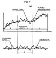
- a measurement of the relative roughness on the surface thereof there is performed such the measurement as pursuant to the definition of a surface roughness and the label thereof (B0601-2001) as defined in the Japanese Industrial Standards (JIS). Moreover, it is one of the points to evaluate an average line thereof, as similar to the method for evaluating such as the Ra thereon, an Rt thereon, the Ry thereon, or the like. Further, according to the above mentioned JIS label, it is able to be evaluated such the average line thereof by making use of a filtered waviness curve.
- a component to be come out to an upper side of such the average line thereof is referred to as a convex component hereinafter, meanwhile, a component to be come out to a lower side of such the average line thereof is defined to be as a concave component hereinafter.
- FIG. 1 that is excerpted from FIG. 1 (a) according to the same JIS label.
- the portion of the roughness curve therein to be come out to the upper side of such the average line therein is defined to be as the convex component therein, meanwhile, the portion thereof to be come out to the lower side thereof is defined to be as the concave component.
- a relative roughness on a surface of a material therefor in a direction as vertical to a rolling therefor there is designed to be measured a relative roughness on a surface of a material therefor in a direction as vertical to a rolling therefor.
- a sampling length thereof is assumed to be as 4 mm, that is to say, a value to be cut off becomes to be as 0.8 mm (that is pursuant to the above mentioned JIS label).
- a rate for scanning thereon is set to be as 0.1 mm/sec.
- a surface roughness measuring apparatus (Surfcorder SE3500) for such the measurement thereof, that is produced by Kosaka Laboratory Ltd.
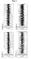
- FIG. 2 For example, there are shown charts ((1), (2), (3), and (4)) in FIG. 2 for showing the relative roughness regarding materials therefor, that are individually produced by following each of a variety of conditions therefor respectively. Still further, there becomes to be sorted the convex components therein and the concave components therein with making use of such the individual charts. And then thereafter, there is performed therefor to be re-plotted, with a vertical axis therein to be redefined as a frequency (%) thereof and a horizontal axis therein to be redefined as a roughness ( ⁇ m) thereon respectively. Hence, there becomes to be obtained FIG. 3 thereby.
- the present invention by forming the Cu-Ni-Si alloy, and also by performing further the addition of at least any one of Sn, Zn, Cr, Mg and Co thereinto, it becomes able to provide the copper alloy, that is superior in such as the strength thereof, the electrical conductivity thereof, the withstand stress and relaxation characteristic (the withstand creep rupture property), the bending workability, the adherence of the solder thereon, or the like, and that becomes to be applicable as preferred to the application of the electrical machinery and apparatus and of the electronic equipment.
- Process group A there is performed a heat treatment therefor at between 425°C and 500°C for between one hour and four hours, and then thereafter there becomes to be performed a sorting therefor into Treatment (1): a material that there is performed an acid cleaning for a surface thereof; Treatment (2) : a material that there is performed to be degreased therefrom; and Treatment (3): a material that there is not performed either one of such the treatments therefor at all. And then thereafter there becomes to be performed a finishing rolling therefor. Thus, it becomes able to be produced each of the materials therefor.
- Treatment (1) there is made use of an aqueous solution of a sulfuric acid as 10% therein
- for Treatment (2) there is made use of hexane, and also there is designed an amount of time for soaking each of thereinto to be as between ten seconds and thirty seconds respectively.
- Process group B there is performed a process of a solution heat treatment for a strip of a t as 0.3 mm at between 850°C and 950°C for between ten seconds and thirty seconds. And then immediately thereafter there becomes to be performed a process of a water quenching therefor.
- a measurement for a material in a direction as vertical to a rolling therefor there is performed a measurement for a material in a direction as vertical to a rolling therefor. Moreover, there is performed such the measurement as pursuant to JIS-B0601 (2001). Further, a length of the measurement therefor is set to be as 4 mm, a value of to be cut off thereof is set to be as 0.8 mm (that is pursuant to the above mentioned JIS label), and a rate for scanning thereon is set to be as 0.1 mm/sec. Still further, there is made use of the surface roughness measuring apparatus (Surfcorder SE3500) for such the measurement therefor, that is produced by Kosaka Laboratory Ltd.
- a result of the assessment therefor is defined to be as making use of a symbol as "double circle (excellent)" in a case where a zero cross time of a meniscograph is shorter than three seconds
- a result of the assessment therefor is defined to be as making use of a symbol of "O (good)” in a case where the zero cross time thereof is not shorter than three seconds but shorter than six seconds
- a result of the assessment therefor is defined to be as making use of a symbol as " ⁇ (acceptable)” in a case where the zero cross time thereof is not shorter than six seconds but shorter than nine seconds
- a result of the assessment therefor is defined to be as making use of a symbol as "X (no good)” in a case where the zero cross time thereof is not shorter than nine seconds.
- the plating of silver thereon there becomes to be performed therefor under a condition that the electric current density therefor is set to be as 1.0 A/dm 2 at a room temperature therefor, in a plating solution that includes potassium silver cyanide as 55 g/l, potassium cyanide as 75 g/l, potassium hydroxide as 10 g/l, and potassium carbonate as 25 g/l. And then after such the plating thereon, there becomes to be performed the assessment by observing any failure on such the plated surface thereof by making use of an optical microscope with a magnification thereof as fifty times therefor.
- Such an copper alloy strip material according to the present invention becomes to be applicable as preferred to such as a lead frame for an electrical machinery and apparatus and for an electronic equipment, a connector therefor, a material for a terminal therefor, or the like, and further to an electrical and an electronic components, such as a connector or a material for a terminal for mounting on a motor vehicle, a relay therefor, a switch therefor, or the like.
Landscapes
- Chemical & Material Sciences (AREA)
- Engineering & Computer Science (AREA)
- Metallurgy (AREA)
- Materials Engineering (AREA)
- Organic Chemistry (AREA)
- Physics & Mathematics (AREA)
- Mechanical Engineering (AREA)
- Power Engineering (AREA)
- Condensed Matter Physics & Semiconductors (AREA)
- Crystallography & Structural Chemistry (AREA)
- Thermal Sciences (AREA)
- General Physics & Mathematics (AREA)
- Microelectronics & Electronic Packaging (AREA)
- Computer Hardware Design (AREA)
- Conductive Materials (AREA)
- Electroplating Methods And Accessories (AREA)
- Lead Frames For Integrated Circuits (AREA)
Applications Claiming Priority (2)
| Application Number | Priority Date | Filing Date | Title |
|---|---|---|---|
| JP2007260397 | 2007-10-03 | ||
| PCT/JP2008/067948 WO2009044822A1 (ja) | 2007-10-03 | 2008-10-02 | 電気・電子部品用銅合金板材 |
Publications (2)
| Publication Number | Publication Date |
|---|---|
| EP2202326A1 true EP2202326A1 (de) | 2010-06-30 |
| EP2202326A4 EP2202326A4 (de) | 2012-06-27 |
Family
ID=40526246
Family Applications (1)
| Application Number | Title | Priority Date | Filing Date |
|---|---|---|---|
| EP08836473A Withdrawn EP2202326A4 (de) | 2007-10-03 | 2008-10-02 | Blechmaterial aus kupferlegierung für elektrische und elektronische bauteile |
Country Status (8)
| Country | Link |
|---|---|
| US (1) | US20100221576A1 (de) |
| EP (1) | EP2202326A4 (de) |
| JP (1) | JP4413992B2 (de) |
| KR (1) | KR100960168B1 (de) |
| CN (1) | CN101809177B (de) |
| MY (1) | MY151391A (de) |
| TW (1) | TWI330202B (de) |
| WO (1) | WO2009044822A1 (de) |
Cited By (1)
| Publication number | Priority date | Publication date | Assignee | Title |
|---|---|---|---|---|
| US20180326543A1 (en) * | 2014-11-11 | 2018-11-15 | Sumitomo Metal Mining Co., Ltd. | Au-Sn-Ag-BASED SOLDER ALLOY AND SOLDER MATERIAL, ELECTRONIC COMPONENT SEALED WITH THE SAME Au-Sn-Ag BASED SOLDER ALLOY OR SOLDER MATERIAL, AND ELECTRONIC COMPONENT MOUNTING DEVICE |
Families Citing this family (17)
| Publication number | Priority date | Publication date | Assignee | Title |
|---|---|---|---|---|
| JP2011025284A (ja) * | 2009-07-27 | 2011-02-10 | Hitachi Cable Ltd | 銅または銅合金材およびその製造方法、並びに半導体パッケージ |
| TWI391952B (zh) * | 2009-09-29 | 2013-04-01 | Jx Nippon Mining & Metals Corp | Cu-Ni-Si-Co based copper alloy for electronic materials and its manufacturing method |
| CN102639732B (zh) * | 2009-12-02 | 2017-08-04 | 古河电气工业株式会社 | 铜合金板材 |
| US9005521B2 (en) * | 2010-04-02 | 2015-04-14 | Jx Nippon Mining & Metals Corporation | Cu—Ni—Si alloy for electronic material |
| JP4831552B1 (ja) | 2011-03-28 | 2011-12-07 | Jx日鉱日石金属株式会社 | Co−Si系銅合金板 |
| WO2012160684A1 (ja) * | 2011-05-25 | 2012-11-29 | 三菱伸銅株式会社 | 深絞り加工性に優れたCu-Ni-Si系銅合金板及びその製造方法 |
| CN103451692A (zh) * | 2012-05-31 | 2013-12-18 | 际华三五二二装具饰品有限公司 | 一种电镀银溶液 |
| JP2014019907A (ja) * | 2012-07-18 | 2014-02-03 | Sh Copper Products Corp | 電気・電子部品用銅合金 |
| JP5362921B1 (ja) * | 2012-11-09 | 2013-12-11 | Jx日鉱日石金属株式会社 | 表面処理銅箔及びそれを用いた積層板 |
| JP2014093425A (ja) * | 2012-11-02 | 2014-05-19 | Sumitomo Metal Mining Co Ltd | Znを主成分とするはんだ合金との接合部を有する電子部品 |
| CN104073677B (zh) * | 2013-03-27 | 2017-01-11 | 株式会社神户制钢所 | Led的引线框用铜合金板条 |
| KR102370860B1 (ko) * | 2014-03-25 | 2022-03-07 | 후루카와 덴키 고교 가부시키가이샤 | 구리합금 판재, 커넥터, 및 구리합금 판재의 제조방법 |
| JP6302009B2 (ja) * | 2016-07-12 | 2018-03-28 | 古河電気工業株式会社 | 銅合金圧延材及びその製造方法並びに電気電子部品 |
| CN114423232A (zh) | 2017-04-28 | 2022-04-29 | 株式会社村田制作所 | 均热板、散热设备以及电子设备 |
| JP7296757B2 (ja) * | 2019-03-28 | 2023-06-23 | Jx金属株式会社 | 銅合金、伸銅品及び電子機器部品 |
| WO2023195267A1 (ja) * | 2022-04-04 | 2023-10-12 | 古河電気工業株式会社 | リードフレーム材およびその製造方法、ならびにリードフレーム材を用いた半導体パッケージ |
| CN115613043A (zh) * | 2022-11-11 | 2023-01-17 | 安徽鑫科铜业有限公司 | 一种铜镍硅合金带材表面处理溶液及铜镍硅合金带材表面处理方法 |
Citations (4)
| Publication number | Priority date | Publication date | Assignee | Title |
|---|---|---|---|---|
| JP2002097534A (ja) * | 2000-09-22 | 2002-04-02 | Nippon Mining & Metals Co Ltd | 高周波回路用銅合金箔 |
| JP2002292406A (ja) * | 2001-03-30 | 2002-10-08 | Nippon Mining & Metals Co Ltd | 電子材料用銅合金、その製造方法、前記電子材料用銅合金に用いる素条、その素条を用いて製造した電子材料用銅合金及びその製造方法 |
| US20030165708A1 (en) * | 2000-07-25 | 2003-09-04 | Takayuki Usami | Copper alloy material for parts of electronic and electric machinery and tools |
| JP2005317463A (ja) * | 2004-04-30 | 2005-11-10 | Nikko Metal Manufacturing Co Ltd | 高周波信号伝送用材料および端子 |
Family Cites Families (11)
| Publication number | Priority date | Publication date | Assignee | Title |
|---|---|---|---|---|
| JP3553775B2 (ja) | 1997-10-16 | 2004-08-11 | ペルメレック電極株式会社 | ガス拡散電極を使用する電解槽 |
| JP3797786B2 (ja) * | 1998-03-06 | 2006-07-19 | 株式会社神戸製鋼所 | 電気・電子部品用銅合金 |
| JP2000288991A (ja) | 1999-04-07 | 2000-10-17 | Naoki Ogawa | 帯刃の曲げと切断の方法と装置 |
| JP2001100581A (ja) | 1999-09-28 | 2001-04-13 | Canon Inc | 加圧用回転体、加熱定着装置及び画像形成装置 |
| JP3760089B2 (ja) * | 2000-07-27 | 2006-03-29 | 日鉱金属加工株式会社 | 高周波回路用銅合金箔 |
| JP4539939B2 (ja) * | 2000-10-30 | 2010-09-08 | 日鉱金属株式会社 | 高周波回路用銅合金箔 |
| JP3824884B2 (ja) * | 2001-05-17 | 2006-09-20 | 古河電気工業株式会社 | 端子ないしはコネクタ用銅合金材 |
| KR100513947B1 (ko) * | 2002-03-29 | 2005-09-09 | 닛코 킨조쿠 가부시키가이샤 | 프레스성이 양호한 구리 합금 소재 및 그 제조방법 |
| JP4538375B2 (ja) * | 2005-05-31 | 2010-09-08 | 日鉱金属株式会社 | プリント配線基板用金属材料 |
| JP2007092118A (ja) * | 2005-09-28 | 2007-04-12 | Nikko Kinzoku Kk | プリント配線基板用金属材料 |
| US8500631B2 (en) | 2006-03-27 | 2013-08-06 | Ethicon Endo-Surgery, Inc. | Methods and devices for percutaneous illumination |
-
2008
- 2008-10-02 CN CN2008801095590A patent/CN101809177B/zh active Active
- 2008-10-02 KR KR1020097006205A patent/KR100960168B1/ko active IP Right Grant
- 2008-10-02 EP EP08836473A patent/EP2202326A4/de not_active Withdrawn
- 2008-10-02 WO PCT/JP2008/067948 patent/WO2009044822A1/ja active Application Filing
- 2008-10-02 US US12/681,512 patent/US20100221576A1/en not_active Abandoned
- 2008-10-02 JP JP2009500654A patent/JP4413992B2/ja active Active
- 2008-10-02 MY MYPI20101498 patent/MY151391A/en unknown
- 2008-10-03 TW TW097138027A patent/TWI330202B/zh active
Patent Citations (4)
| Publication number | Priority date | Publication date | Assignee | Title |
|---|---|---|---|---|
| US20030165708A1 (en) * | 2000-07-25 | 2003-09-04 | Takayuki Usami | Copper alloy material for parts of electronic and electric machinery and tools |
| JP2002097534A (ja) * | 2000-09-22 | 2002-04-02 | Nippon Mining & Metals Co Ltd | 高周波回路用銅合金箔 |
| JP2002292406A (ja) * | 2001-03-30 | 2002-10-08 | Nippon Mining & Metals Co Ltd | 電子材料用銅合金、その製造方法、前記電子材料用銅合金に用いる素条、その素条を用いて製造した電子材料用銅合金及びその製造方法 |
| JP2005317463A (ja) * | 2004-04-30 | 2005-11-10 | Nikko Metal Manufacturing Co Ltd | 高周波信号伝送用材料および端子 |
Non-Patent Citations (1)
| Title |
|---|
| See also references of WO2009044822A1 * |
Cited By (2)
| Publication number | Priority date | Publication date | Assignee | Title |
|---|---|---|---|---|
| US20180326543A1 (en) * | 2014-11-11 | 2018-11-15 | Sumitomo Metal Mining Co., Ltd. | Au-Sn-Ag-BASED SOLDER ALLOY AND SOLDER MATERIAL, ELECTRONIC COMPONENT SEALED WITH THE SAME Au-Sn-Ag BASED SOLDER ALLOY OR SOLDER MATERIAL, AND ELECTRONIC COMPONENT MOUNTING DEVICE |
| US10589387B2 (en) * | 2014-11-11 | 2020-03-17 | Sumitomo Metal Mining Co., Ltd. | Au—Sn—Ag-based solder alloy and solder material, electronic component sealed with the same Au—Sn—Ag based solder alloy or solder material, and electronic component mounting device |
Also Published As
| Publication number | Publication date |
|---|---|
| JP4413992B2 (ja) | 2010-02-10 |
| EP2202326A4 (de) | 2012-06-27 |
| US20100221576A1 (en) | 2010-09-02 |
| WO2009044822A1 (ja) | 2009-04-09 |
| CN101809177A (zh) | 2010-08-18 |
| KR20090088850A (ko) | 2009-08-20 |
| TWI330202B (en) | 2010-09-11 |
| KR100960168B1 (ko) | 2010-05-26 |
| CN101809177B (zh) | 2011-09-07 |
| TW200927960A (en) | 2009-07-01 |
| JPWO2009044822A1 (ja) | 2011-02-10 |
| MY151391A (en) | 2014-05-30 |
Similar Documents
| Publication | Publication Date | Title |
|---|---|---|
| EP2202326A1 (de) | Blechmaterial aus kupferlegierung für elektrische und elektronische bauteile | |
| KR101136265B1 (ko) | 전기 전자 부품용 구리 합금판 | |
| EP2216426B1 (de) | Verzinntes material für elektronisches bauteil | |
| EP2695956B1 (de) | Kupferlegierungsblech | |
| EP1889934B1 (de) | Kupferlegierungsplatte und herstellungsverfahren dafür | |
| EP2298945B1 (de) | Folienmaterial aus kupferlegierung und verfahren zur herstellung davon | |
| EP2221390B1 (de) | Verfahren zur herstellung eines kupferlegierungsbleches mit hervorragender festigkeit, biegebearbeitbarkeit und spannungsrelaxationsresistenz | |
| EP2319947A1 (de) | Kupferlegierungsmaterial für elektrische und elektronische bauteile sowie herstellungsverfahren dafür | |
| EP2333127A1 (de) | Kupferlegierungsmaterial für elektrische und elektronische bauteile | |
| EP2636769A2 (de) | Kupferlegierungsfolie mit Sn-Überzugsschicht für eine Passverbindungsklemme und Passverbindungsklemme | |
| EP2484812B1 (de) | Aus sn oder einer sn-legierung plattierter film sowie verbundmaterial damit | |
| TWI392753B (zh) | Ni-Si-Co-based copper alloy and a method for producing the same | |
| TWI418642B (zh) | Cu-Co-Si copper alloy rolling plate and electrical parts using the same | |
| TWI541367B (zh) | Cu-Ni-Si type copper alloy sheet having good mold resistance and shearing workability and manufacturing method thereof | |
| EP2221391A1 (de) | Kupferlegierungsblechmaterial | |
| JP3797786B2 (ja) | 電気・電子部品用銅合金 | |
| KR20190077011A (ko) | 구리 합금 판재 및 그 제조 방법 | |
| EP2243847A1 (de) | Kupferlegierungsmaterial für elektrische und elektronische bauteile | |
| TWI422693B (zh) | Cu-Co-Si alloy sheet and method for producing the same | |
| JPH10219372A (ja) | 電気、電子部品用銅合金とその製造方法 | |
| JP5339995B2 (ja) | Cu−Zn−Sn系合金板及びCu−Zn−Sn系合金Snめっき条 | |
| JP2007169764A (ja) | 銅合金 | |
| JP2006274422A (ja) | プレス打抜き性に優れた電子部品用素材 | |
| EP3604575A1 (de) | Kupferlegierungsband mit verbesserter formgenauigkeit nach einer pressbearbeitung | |
| EP4261329A1 (de) | Ag-beschichtetes material, herstellungsverfahren für ag-beschichtetes material und endgerätekomponente |
Legal Events
| Date | Code | Title | Description |
|---|---|---|---|
| PUAI | Public reference made under article 153(3) epc to a published international application that has entered the european phase |
Free format text: ORIGINAL CODE: 0009012 |
|
| 17P | Request for examination filed |
Effective date: 20100331 |
|
| AK | Designated contracting states |
Kind code of ref document: A1 Designated state(s): AT BE BG CH CY CZ DE DK EE ES FI FR GB GR HR HU IE IS IT LI LT LU LV MC MT NL NO PL PT RO SE SI SK TR |
|
| AX | Request for extension of the european patent |
Extension state: AL BA MK RS |
|
| DAX | Request for extension of the european patent (deleted) | ||
| A4 | Supplementary search report drawn up and despatched |
Effective date: 20120531 |
|
| RIC1 | Information provided on ipc code assigned before grant |
Ipc: C22F 1/00 20060101ALI20120523BHEP Ipc: H01L 23/48 20060101ALI20120523BHEP Ipc: C22F 1/08 20060101ALI20120523BHEP Ipc: C22C 9/06 20060101AFI20120523BHEP |
|
| 17Q | First examination report despatched |
Effective date: 20130207 |
|
| STAA | Information on the status of an ep patent application or granted ep patent |
Free format text: STATUS: THE APPLICATION HAS BEEN WITHDRAWN |
|
| 18W | Application withdrawn |
Effective date: 20130628 |