EP2636769A2 - Kupferlegierungsfolie mit Sn-Überzugsschicht für eine Passverbindungsklemme und Passverbindungsklemme - Google Patents
Kupferlegierungsfolie mit Sn-Überzugsschicht für eine Passverbindungsklemme und Passverbindungsklemme Download PDFInfo
- Publication number
- EP2636769A2 EP2636769A2 EP13001120.8A EP13001120A EP2636769A2 EP 2636769 A2 EP2636769 A2 EP 2636769A2 EP 13001120 A EP13001120 A EP 13001120A EP 2636769 A2 EP2636769 A2 EP 2636769A2
- Authority
- EP
- European Patent Office
- Prior art keywords
- coating layer
- copper alloy
- mass
- less
- alloy sheet
- Prior art date
- Legal status (The legal status is an assumption and is not a legal conclusion. Google has not performed a legal analysis and makes no representation as to the accuracy of the status listed.)
- Withdrawn
Links
- 239000011247 coating layer Substances 0.000 title claims abstract description 191
- 229910000881 Cu alloy Inorganic materials 0.000 title claims abstract description 99
- 239000000463 material Substances 0.000 claims abstract description 89
- 229910045601 alloy Inorganic materials 0.000 claims abstract description 72
- 239000000956 alloy Substances 0.000 claims abstract description 72
- 229910017755 Cu-Sn Inorganic materials 0.000 claims abstract description 67
- 229910017927 Cu—Sn Inorganic materials 0.000 claims abstract description 67
- KUNSUQLRTQLHQQ-UHFFFAOYSA-N copper tin Chemical group [Cu].[Sn] KUNSUQLRTQLHQQ-UHFFFAOYSA-N 0.000 claims abstract description 67
- 238000005096 rolling process Methods 0.000 claims abstract description 52
- 229910017876 Cu—Ni—Si Inorganic materials 0.000 claims abstract description 30
- 238000003780 insertion Methods 0.000 claims abstract description 14
- 230000037431 insertion Effects 0.000 claims abstract description 14
- 239000010949 copper Substances 0.000 claims description 25
- 229910052759 nickel Inorganic materials 0.000 claims description 11
- 229910052802 copper Inorganic materials 0.000 claims description 9
- 239000012535 impurity Substances 0.000 claims description 3
- 238000007747 plating Methods 0.000 description 49
- 239000000523 sample Substances 0.000 description 34
- 230000003746 surface roughness Effects 0.000 description 26
- 239000010410 layer Substances 0.000 description 20
- 238000005452 bending Methods 0.000 description 18
- 238000005259 measurement Methods 0.000 description 18
- 239000000203 mixture Substances 0.000 description 15
- 239000002345 surface coating layer Substances 0.000 description 15
- 238000005260 corrosion Methods 0.000 description 12
- 230000007797 corrosion Effects 0.000 description 12
- 238000001816 cooling Methods 0.000 description 7
- 238000012360 testing method Methods 0.000 description 7
- 229910052718 tin Inorganic materials 0.000 description 7
- 238000005097 cold rolling Methods 0.000 description 6
- 238000009792 diffusion process Methods 0.000 description 6
- 230000032683 aging Effects 0.000 description 5
- 238000005098 hot rolling Methods 0.000 description 5
- 238000011088 calibration curve Methods 0.000 description 4
- 238000005336 cracking Methods 0.000 description 4
- 238000011156 evaluation Methods 0.000 description 4
- 238000000227 grinding Methods 0.000 description 4
- 238000004519 manufacturing process Methods 0.000 description 4
- 238000000034 method Methods 0.000 description 4
- 230000007928 solubilization Effects 0.000 description 4
- 238000005063 solubilization Methods 0.000 description 4
- XLYOFNOQVPJJNP-UHFFFAOYSA-N water Substances O XLYOFNOQVPJJNP-UHFFFAOYSA-N 0.000 description 4
- HEMHJVSKTPXQMS-UHFFFAOYSA-M Sodium hydroxide Chemical compound [OH-].[Na+] HEMHJVSKTPXQMS-UHFFFAOYSA-M 0.000 description 3
- 238000005266 casting Methods 0.000 description 3
- 230000000694 effects Effects 0.000 description 3
- 238000010438 heat treatment Methods 0.000 description 3
- 238000002844 melting Methods 0.000 description 3
- 230000008018 melting Effects 0.000 description 3
- 239000002244 precipitate Substances 0.000 description 3
- 238000004439 roughness measurement Methods 0.000 description 3
- 239000006104 solid solution Substances 0.000 description 3
- FAPWRFPIFSIZLT-UHFFFAOYSA-M Sodium chloride Chemical compound [Na+].[Cl-] FAPWRFPIFSIZLT-UHFFFAOYSA-M 0.000 description 2
- QAOWNCQODCNURD-UHFFFAOYSA-N Sulfuric acid Chemical compound OS(O)(=O)=O QAOWNCQODCNURD-UHFFFAOYSA-N 0.000 description 2
- 238000000137 annealing Methods 0.000 description 2
- 238000007796 conventional method Methods 0.000 description 2
- 230000003247 decreasing effect Effects 0.000 description 2
- UREBDLICKHMUKA-CXSFZGCWSA-N dexamethasone Chemical compound C1CC2=CC(=O)C=C[C@]2(C)[C@]2(F)[C@@H]1[C@@H]1C[C@@H](C)[C@@](C(=O)CO)(O)[C@@]1(C)C[C@@H]2O UREBDLICKHMUKA-CXSFZGCWSA-N 0.000 description 2
- 229910052742 iron Inorganic materials 0.000 description 2
- 230000000644 propagated effect Effects 0.000 description 2
- 238000010791 quenching Methods 0.000 description 2
- 230000000171 quenching effect Effects 0.000 description 2
- 238000001953 recrystallisation Methods 0.000 description 2
- 150000003839 salts Chemical class 0.000 description 2
- 238000002791 soaking Methods 0.000 description 2
- 239000000243 solution Substances 0.000 description 2
- 238000005507 spraying Methods 0.000 description 2
- 229910052726 zirconium Inorganic materials 0.000 description 2
- BZOVBIIWPDQIHF-UHFFFAOYSA-N 3-hydroxy-2-methylbenzenesulfonic acid Chemical compound CC1=C(O)C=CC=C1S(O)(=O)=O BZOVBIIWPDQIHF-UHFFFAOYSA-N 0.000 description 1
- BTJIUGUIPKRLHP-UHFFFAOYSA-N 4-nitrophenol Chemical compound OC1=CC=C([N+]([O-])=O)C=C1 BTJIUGUIPKRLHP-UHFFFAOYSA-N 0.000 description 1
- 229910020711 Co—Si Inorganic materials 0.000 description 1
- 229910018104 Ni-P Inorganic materials 0.000 description 1
- 229910005487 Ni2Si Inorganic materials 0.000 description 1
- 229910021586 Nickel(II) chloride Inorganic materials 0.000 description 1
- 229910018536 Ni—P Inorganic materials 0.000 description 1
- 239000006061 abrasive grain Substances 0.000 description 1
- 230000002180 anti-stress Effects 0.000 description 1
- 239000007864 aqueous solution Substances 0.000 description 1
- 230000004888 barrier function Effects 0.000 description 1
- 230000015572 biosynthetic process Effects 0.000 description 1
- 150000001875 compounds Chemical class 0.000 description 1
- ARUVKPQLZAKDPS-UHFFFAOYSA-L copper(II) sulfate Chemical compound [Cu+2].[O-][S+2]([O-])([O-])[O-] ARUVKPQLZAKDPS-UHFFFAOYSA-L 0.000 description 1
- 229910000366 copper(II) sulfate Inorganic materials 0.000 description 1
- 239000013078 crystal Substances 0.000 description 1
- 238000010191 image analysis Methods 0.000 description 1
- 229910000765 intermetallic Inorganic materials 0.000 description 1
- 239000002184 metal Substances 0.000 description 1
- 229910052751 metal Inorganic materials 0.000 description 1
- QMMRZOWCJAIUJA-UHFFFAOYSA-L nickel dichloride Chemical compound Cl[Ni]Cl QMMRZOWCJAIUJA-UHFFFAOYSA-L 0.000 description 1
- LGQLOGILCSXPEA-UHFFFAOYSA-L nickel sulfate Chemical compound [Ni+2].[O-]S([O-])(=O)=O LGQLOGILCSXPEA-UHFFFAOYSA-L 0.000 description 1
- 229910000363 nickel(II) sulfate Inorganic materials 0.000 description 1
- 230000003647 oxidation Effects 0.000 description 1
- 238000007254 oxidation reaction Methods 0.000 description 1
- 239000002245 particle Substances 0.000 description 1
- 238000001556 precipitation Methods 0.000 description 1
- 238000012545 processing Methods 0.000 description 1
- 238000007670 refining Methods 0.000 description 1
- 238000000926 separation method Methods 0.000 description 1
- 239000002356 single layer Substances 0.000 description 1
- 239000011780 sodium chloride Substances 0.000 description 1
- 230000001629 suppression Effects 0.000 description 1
- 229910000375 tin(II) sulfate Inorganic materials 0.000 description 1
- 229910052725 zinc Inorganic materials 0.000 description 1
Images

Classifications
-
- H—ELECTRICITY
- H01—ELECTRIC ELEMENTS
- H01R—ELECTRICALLY-CONDUCTIVE CONNECTIONS; STRUCTURAL ASSOCIATIONS OF A PLURALITY OF MUTUALLY-INSULATED ELECTRICAL CONNECTING ELEMENTS; COUPLING DEVICES; CURRENT COLLECTORS
- H01R13/00—Details of coupling devices of the kinds covered by groups H01R12/70 or H01R24/00 - H01R33/00
- H01R13/02—Contact members
- H01R13/03—Contact members characterised by the material, e.g. plating, or coating materials
-
- C—CHEMISTRY; METALLURGY
- C25—ELECTROLYTIC OR ELECTROPHORETIC PROCESSES; APPARATUS THEREFOR
- C25D—PROCESSES FOR THE ELECTROLYTIC OR ELECTROPHORETIC PRODUCTION OF COATINGS; ELECTROFORMING; APPARATUS THEREFOR
- C25D5/00—Electroplating characterised by the process; Pretreatment or after-treatment of workpieces
- C25D5/10—Electroplating with more than one layer of the same or of different metals
- C25D5/12—Electroplating with more than one layer of the same or of different metals at least one layer being of nickel or chromium
-
- B—PERFORMING OPERATIONS; TRANSPORTING
- B32—LAYERED PRODUCTS
- B32B—LAYERED PRODUCTS, i.e. PRODUCTS BUILT-UP OF STRATA OF FLAT OR NON-FLAT, e.g. CELLULAR OR HONEYCOMB, FORM
- B32B15/00—Layered products comprising a layer of metal
- B32B15/01—Layered products comprising a layer of metal all layers being exclusively metallic
-
- C—CHEMISTRY; METALLURGY
- C22—METALLURGY; FERROUS OR NON-FERROUS ALLOYS; TREATMENT OF ALLOYS OR NON-FERROUS METALS
- C22C—ALLOYS
- C22C9/00—Alloys based on copper
- C22C9/02—Alloys based on copper with tin as the next major constituent
-
- C—CHEMISTRY; METALLURGY
- C22—METALLURGY; FERROUS OR NON-FERROUS ALLOYS; TREATMENT OF ALLOYS OR NON-FERROUS METALS
- C22C—ALLOYS
- C22C9/00—Alloys based on copper
- C22C9/06—Alloys based on copper with nickel or cobalt as the next major constituent
-
- C—CHEMISTRY; METALLURGY
- C22—METALLURGY; FERROUS OR NON-FERROUS ALLOYS; TREATMENT OF ALLOYS OR NON-FERROUS METALS
- C22F—CHANGING THE PHYSICAL STRUCTURE OF NON-FERROUS METALS AND NON-FERROUS ALLOYS
- C22F1/00—Changing the physical structure of non-ferrous metals or alloys by heat treatment or by hot or cold working
- C22F1/08—Changing the physical structure of non-ferrous metals or alloys by heat treatment or by hot or cold working of copper or alloys based thereon
-
- C—CHEMISTRY; METALLURGY
- C25—ELECTROLYTIC OR ELECTROPHORETIC PROCESSES; APPARATUS THEREFOR
- C25D—PROCESSES FOR THE ELECTROLYTIC OR ELECTROPHORETIC PRODUCTION OF COATINGS; ELECTROFORMING; APPARATUS THEREFOR
- C25D5/00—Electroplating characterised by the process; Pretreatment or after-treatment of workpieces
- C25D5/48—After-treatment of electroplated surfaces
- C25D5/50—After-treatment of electroplated surfaces by heat-treatment
- C25D5/505—After-treatment of electroplated surfaces by heat-treatment of electroplated tin coatings, e.g. by melting
-
- C—CHEMISTRY; METALLURGY
- C25—ELECTROLYTIC OR ELECTROPHORETIC PROCESSES; APPARATUS THEREFOR
- C25D—PROCESSES FOR THE ELECTROLYTIC OR ELECTROPHORETIC PRODUCTION OF COATINGS; ELECTROFORMING; APPARATUS THEREFOR
- C25D5/00—Electroplating characterised by the process; Pretreatment or after-treatment of workpieces
- C25D5/60—Electroplating characterised by the structure or texture of the layers
- C25D5/605—Surface topography of the layers, e.g. rough, dendritic or nodular layers
-
- C—CHEMISTRY; METALLURGY
- C25—ELECTROLYTIC OR ELECTROPHORETIC PROCESSES; APPARATUS THEREFOR
- C25D—PROCESSES FOR THE ELECTROLYTIC OR ELECTROPHORETIC PRODUCTION OF COATINGS; ELECTROFORMING; APPARATUS THEREFOR
- C25D7/00—Electroplating characterised by the article coated
-
- C—CHEMISTRY; METALLURGY
- C25—ELECTROLYTIC OR ELECTROPHORETIC PROCESSES; APPARATUS THEREFOR
- C25D—PROCESSES FOR THE ELECTROLYTIC OR ELECTROPHORETIC PRODUCTION OF COATINGS; ELECTROFORMING; APPARATUS THEREFOR
- C25D3/00—Electroplating: Baths therefor
- C25D3/02—Electroplating: Baths therefor from solutions
- C25D3/12—Electroplating: Baths therefor from solutions of nickel or cobalt
-
- C—CHEMISTRY; METALLURGY
- C25—ELECTROLYTIC OR ELECTROPHORETIC PROCESSES; APPARATUS THEREFOR
- C25D—PROCESSES FOR THE ELECTROLYTIC OR ELECTROPHORETIC PRODUCTION OF COATINGS; ELECTROFORMING; APPARATUS THEREFOR
- C25D3/00—Electroplating: Baths therefor
- C25D3/02—Electroplating: Baths therefor from solutions
- C25D3/30—Electroplating: Baths therefor from solutions of tin
-
- C—CHEMISTRY; METALLURGY
- C25—ELECTROLYTIC OR ELECTROPHORETIC PROCESSES; APPARATUS THEREFOR
- C25D—PROCESSES FOR THE ELECTROLYTIC OR ELECTROPHORETIC PRODUCTION OF COATINGS; ELECTROFORMING; APPARATUS THEREFOR
- C25D3/00—Electroplating: Baths therefor
- C25D3/02—Electroplating: Baths therefor from solutions
- C25D3/38—Electroplating: Baths therefor from solutions of copper
-
- C—CHEMISTRY; METALLURGY
- C25—ELECTROLYTIC OR ELECTROPHORETIC PROCESSES; APPARATUS THEREFOR
- C25D—PROCESSES FOR THE ELECTROLYTIC OR ELECTROPHORETIC PRODUCTION OF COATINGS; ELECTROFORMING; APPARATUS THEREFOR
- C25D3/00—Electroplating: Baths therefor
- C25D3/02—Electroplating: Baths therefor from solutions
- C25D3/56—Electroplating: Baths therefor from solutions of alloys
- C25D3/58—Electroplating: Baths therefor from solutions of alloys containing more than 50% by weight of copper
-
- Y—GENERAL TAGGING OF NEW TECHNOLOGICAL DEVELOPMENTS; GENERAL TAGGING OF CROSS-SECTIONAL TECHNOLOGIES SPANNING OVER SEVERAL SECTIONS OF THE IPC; TECHNICAL SUBJECTS COVERED BY FORMER USPC CROSS-REFERENCE ART COLLECTIONS [XRACs] AND DIGESTS
- Y10—TECHNICAL SUBJECTS COVERED BY FORMER USPC
- Y10T—TECHNICAL SUBJECTS COVERED BY FORMER US CLASSIFICATION
- Y10T428/00—Stock material or miscellaneous articles
- Y10T428/12—All metal or with adjacent metals
- Y10T428/12493—Composite; i.e., plural, adjacent, spatially distinct metal components [e.g., layers, joint, etc.]
- Y10T428/12708—Sn-base component
- Y10T428/12715—Next to Group IB metal-base component
Definitions
- the present invention relates to a copper alloy sheet with Sn coating layer for a fitting type connection terminal and a fitting type connection terminal produced from the copper alloy sheet with the Sn coating layer.
- connection terminal As a connector used for connecting an electric wire for automobiles or the like, a fitting type connection terminal composed of a male terminal and a female terminal has been used. In recent years, this kind of connection terminal tends to be made compact and multipolar because of weight saving and miniaturization of parts.
- Fitting of a connection terminal is performed manually and a connection terminal produced from a copper alloy sheet with Sn coating layer sheet requires high insertion force at the time of fitting if the number of poles is large. Therefore, in terms of reduction of the load on a worker, it is strongly required to reduce the insertion force of a connection terminal. At the same time, it is also required to reliably maintain the electric characteristics (low contact resistance) even after a long duration at a high temperature.
- JP A Japanese Patent Application Laid-Open
- JP A No. 2004-68026 proposes a copper alloy sheet with Sn coating layer obtained by forming a surface coating layer composed of a Ni coating layer, a Cu-Sn alloy coating layer, and a Sn coating layer in this order on a surface of a copper alloy sheet.
- JP A No. 2006-183068 proposes a copper alloy sheet with Sn coating layer obtained by forming a surface coating layer composed of either a Cu-Sn alloy coating layer in combination with a Sn coating layer or a Ni coating layer in combination with a Cu-Sn alloy coating layer and a Sn coating layer in this order on a surface-roughened surface of a copper alloy sheet and exposing the Cu-Sn alloy coating layer to the outermost surface at a predetermined area rate.
- JP A No. 2004-339555 proposes a copper alloy sheet with Sn coating layer obtained by forming a Ni or Cu under-plating layer and a Sn plating layer on a surface of a copper alloy sheet and carrying out reflow treatment to make hard regions and soft regions coexist in the surface coating layer.
- JP A No. 2009-135097 proposes a copper alloy sheet with Sn coating layer obtained by forming a surface coating layer composed of a Ni coating layer, a Cu coating layer, a Cu-Sn alloy coating layer, and a Sn coating layer on a surface of a copper alloy sheet so that the Cu-Sn alloy coating layer and the Sn coating layer coexist in the surface coating layer, and so that neighboring Cu-Sn alloy particles of the Cu-Sn alloy coating layer are integrated.
- the copper alloy sheet with the Sn coating layer described in JP A No. 2004-68026 is insufficient in reducing the friction coefficient (reducing the insertion force).
- the copper alloy sheet with the Sn coating layer described in JP A No. 2006-183068 can further reduce the friction coefficient (the insertion force) since the Cu-Sn alloy coating layer is exposed to the outermost surface at a predetermined area rate.
- carrying out a step for making the surface of the copper alloy sheet base material uneven is necessary before plating, which results in increase of the cost.
- the copper alloy sheet with the Sn coating layer described in JP-A No. 2004-339555 requires carrying out a heat treatment step of segregating the alloy elements or forming oxides in grain boundaries of the copper alloy base material before plating.
- the copper alloy sheet with the Sn coating layer described in JP-A No. 2009-135097 requires special reflow and cooling conditions. Both cases result in increase of the cost in their production.
- Inventors of the present invention produced a thin sheet of a Cu-Ni-Si system copper alloy, generally known in the name of Corson alloy, by a conventional method.
- the inventors obtained a copper alloy sheet with Sn coating layer having a surface coating layer composed of a Ni coating layer, a Cu-Sn alloy coating layer, and a Sn coating layer by forming a Ni plating layer, a Cu plating layer, and a Sn plating layer in this order on the base material surface and thereafter carrying out reflow treatment as the invention described in JP A No. 2004-68026 .
- the respective layers before the reflow treatment are called as “plating layers” and the respective layers after the reflow treatment are called as "coating layers”.
- the surface roughness (arithmetic mean roughness Ra) of the Cu-Ni-Si system copper alloy as the base material is not intentionally made high as that for the copper alloy base material of JP A No. 2006-183068 but made to be a normal level. Unlike that in the invention described in JP A No. 2004-339555 , no special heat treatment before plating is carried out. Unlike those in the invention described in JP-A No. 2009-135097 , employed reflow treatment and subsequent cooling condition are not special and very common conditions.
- the inventors of the present invention have measured the friction coefficient of this copper alloy sheet with Sn coating layer and have found that the friction coefficient was apparently smaller particularly in the perpendicular direction to the rolling direction than that of a conventional copper alloy sheet with Sn coating layer having a surface entirely coated with the Sn coating layer and that the friction coefficient was approximately an intermediate value between those of the inventions described in JP-A No. 2004-68026 and JP-A No. 2006-183068 .
- a copper alloy sheet with Sn coating layer for a fitting type connection terminal of the present invention comprises a base material made of Cu-Ni-Si system copper alloy, a Ni coating layer formed on the base material and having an average thickness of 0.1 to 0.8 ⁇ m, a Cu-Sn alloy coating layer formed on the Ni coating layer and having an average thickness of 0.4 to 1.0 ⁇ m, and an Sn coating layer formed on the Cu-Sn alloy coating layer and having an average thickness of 0.1 to 0.8 ⁇ m.
- a material surface is subject to reflow treatment and has arithmetic mean roughness Ra of 0.03 ⁇ m or more and less than 0.15 ⁇ m in both a direction parallel to a rolling direction and a direction perpendicular to the rolling direction.
- An exposure rate of the Cu-Sn alloy coating layer to the material surface is 10 to 50%.
- the above-mentioned copper alloy sheet with Sn coating layer for a fitting type connection terminal has the following desirable embodiments.
- the Cu-Sn alloy coating layer is exposed the material surface so as to linearly extend in the direction parallel to the rolling direction.
- the surface of the base material is buffed along the direction parallel to the rolling direction.
- Arithmetic mean roughness Ra of the surface of the base material in the direction parallel to the rolling direction is 0.05 ⁇ m or more and less than 0.20 ⁇ m and arithmetic mean roughness Ra in the direction perpendicular to the rolling direction is 0.07 ⁇ m or more and less than 0.20 ⁇ m.
- the copper alloy sheet with Sn coating layer of the present invention Since the Cu-Sn alloy coating layer is exposed to the outermost surface of the surface coating layer at a predetermined area rate, the copper alloy sheet with Sn coating layer of the present invention has a low friction coefficient as compared with that in the case where the Sn coating layer covers the entire surface of the surface coating layer. Therefore, using this copper alloy sheet with Sn coating layer is used for one or both of a male terminal and a female terminal of a fitting type connection terminal can reduce the insertion force at the time of fitting.
- the copper alloy sheet with Sn coating layer of the present invention is also excellent in corrosion resistance and bending processability as well as the electric characteristics (low contact resistance) after a long duration at a high temperature.
- the copper alloy sheet with Sn coating layer of the present invention can be produced by using a common Cu-Ni-Si system copper alloy sheet as a base material, carrying out Ni plating, Cu plating, and Sn plating in this order, and subsequently carrying out reflow treatment.
- An alloy sheet having a common surface roughness may be used as the Cu-Ni-Si system copper alloy sheet with no need of special heat treatment or the like before the plating, and further a common reflow treatment and a common cooling condition are applicable. Consequently, the copper alloy sheet with Sn coating layer of the present invention can be produced at a low production cost as compared with that of the copper alloy sheet with Sn coating layer described in JP-A No. 2006-183068 .
- Fig. 1 is a SEM composition image of a surface of a sample material of Embodiment No. 3;
- Fig. 2 is a binarized composition image of the sample material
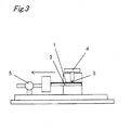
- Fig. 3 is a conceptual illustration of a friction coefficient measurement apparatus.
- a Cu-Ni-Si system copper alloy sheet generally known in the name of Corson alloy is used.
- a desirable composition is Ni: 1 to 4% by mass; Si: 0.2 to 0.9% by mass, and the balance consisting of Cu and inevitable impurities.
- the composition may further contain any one or more of Sn: 3% by mass or less, Mg: 0.5% by mass or less, Zn: 2.0% by mass or less, Mn: 0.5% by mass or less, Cr: 0.3% by mass or less, Zr: 0.1% by mass or less, P: 0.1% by mass or less; Fe: 0.3% by mass or less; and Co: 1.5% by mass or less.
- composition itself is known well and there are many compositions practically used as a fitting type connection terminal, for example, C64725 (Cu-2%Ni-0.5%Si-1%Zn-0.5%Sn), C64760 (Cu-1.8% Ni-0.4% Si-1.1% Zn-0.1% Sn), C64785 (Cu-3.2% Ni-0.7% Si-0.5% Sn-1% Zn), C70250 (Cu-3.0% Ni-0.65% Si-0.15% Mg), and C70350 (Cu-1.5% N-1.1% Co-0.6% Si) that are standardized by ASTM.
- C64725 Cu-2%Ni-0.5%Si-1%Zn-0.5%Sn
- C64760 Cu-1.8% Ni-0.4% Si-1.1% Zn-0.1% Sn
- C64785 Cu-3.2% Ni-0.7% Si-0.5% Sn-1% Zn
- C70250 Cu-3.0% Ni-0.65% Si-0.15% Mg
- C70350 Cu-1.5% N-1.1% Co-0.6% Si
- Ni and Si are elements which improve the strength by forming a precipitate of Ni 2 Si.
- the Ni content is 1 to 4% by mass and the Si content is desirably in the range of 0.2 to 0.9% by mass so as to give a Ni/Si mass ratio of 3.5 to 5.5 corresponding to the Ni content. If the Ni content is less than 1% by mass or the Si content is less than 0.2% by mass, the strength becomes insufficient. If the Ni content exceeds 4% by mass or the Si content exceeds 0.9% by mass, Ni or Si is crystallized or precipitated at the time of casting to lower the hot workability. In the case where the Ni/Si mass ratio is less than 3.5 or exceeds 5.5, the excess Ni or Si forms a solid solution to lower conductivity.
- the Ni content is preferably 1.7 to 3.9% by mass.
- the Ni/Si mass ratio is preferably 4.0 to 5.0.
- Sn improves the strength characteristic and anti-stress relief characteristic by forming a solid solution in the structure, but if its content exceeds 3% by mass, the conductivity and bending processability are deteriorated. Consequently, in the case where Sn is added, the content is adjusted to 3% by mass or less and preferably 2.0% by mass or less.
- Mg improves the strength characteristic by forming a solid solution in the structure, but if its content exceeds 0.5% by mass, the bending processability and conductivity are deteriorated. Consequently, in the case where Mg is added, the content is adjusted to 0.5% by mass or less and preferably 0.3% by mass or less.
- Cr improves the hot workability, but if its content exceeds 0.3% by mass, a precipitate is produced to lower the bending processability. Consequently, in the case where Cr is added, the content is adjusted to 0.3% by mass or less and preferably 0.1% by mass or less.
- Mn improves the hot workability, but if its content exceeds 0.5% by mass, the conductivity is reduced. Consequently, in the case where Mn is added, the content is adjusted to 0.5% by mass or less and preferably 0.3% by mass or less.
- Zn improves the peeling resistance of the Sn plating, but if its content exceeds 2.0% by mass, the bending processability and conductivity are deteriorated. Consequently, in the case where Zn is added, the content is adjusted to 2.0% by mass or less and preferably 1.5% by mass or less.
- Zr and Fe have an action of refining crystal grains, but if their contents exceed 0.1% by mass and 0.3% by mass, respectively, the bending processability is deteriorated. Consequently, in the case where Zr and Fe are added, the contents are adjusted to 0.1% by mass or less and 0.3% by mass or less, respectively, and preferably 0.05% by mass or less and 0.1% by mass or less, respectively.
- P is an element which contributes mainly to the improvement of soundness (deacidification and molten metal flow) for an ingot. Consequently, in the case of improving the soundness for an ingot, P is added. If P is added in a content of 0.1 % or more, a Ni-P intermetallic compound is easily precipitated, agglomerated, and coarsened to cause cracking at the time of hot working and lowering of the workability. Consequently, in the case where P is added, the content is adjusted to 0.1% by mass or less and preferably 0.03% by mass or less.
- Co is an element for producing a Ni-Co-Si type precipitate to further improve the strength of the copper alloy.
- the content of Co exceeds 1.5% by mass, the precipitation amount of the compound in an ingot is increased and it tends to cause cracking of an ingot, heat cracking at the time of hot rolling, and heat stretching cracking. Consequently, the Co content is adjusted to 1.5% by mass or less.
- the Co content is preferably 0.05% by mass or more. It is preferable that the composition is determined so as to adjust the total content of Ni and Co to 1 to 4% by mass and the (Ni + Co) / Si mass ratio to 3.5 to 5.5 and preferably 4.0 to 5.0.
- a Cu-Ni-Si system copper alloy sheet according to the present invention can be produced according to a conventional method by carrying out steps of melting/ casting, soaking, hot rolling, quenching after hot rolling, cold rolling, recrystallizing accompanied with solubilization, cold rolling, and aging.
- the cold rolling unlike the invention described in JP-A No. 2006-183068 , there is no need to use surface-roughened work rolls and rolls with normal surface roughness may be used.
- steps of recrystallizing accompanied with solubilization, aging, and cold rolling may be selected. Further, in order to obtain a good spring property, low temperature annealing may be carried out at the last.
- a grinding step for removing an oxide film on the surface is carried out after the recrystallization treatment, aging treatment, and low temperature annealing.
- a rotating buff is preferably used for this grinding step and is commonly used.
- a rotating buff is arranged in a manner that its rotary shaft is perpendicular to the rolling direction and the buff is pushed against the surface of the Cu-Ni-Si system copper alloy sheet which is continuously moved in the longitudinal direction.
- the Cu-Ni-Si system copper alloy sheet obtained by the above-mentioned method is not at all different from a common Cu-Ni-Si system copper alloy sheet.
- the arithmetic mean roughness Ra in the direction parallel to the rolling direction is 0.05 ⁇ m or more and less than 0.20 ⁇ m and more generally 0.07 ⁇ m or more and 0.15 ⁇ m or less and the arithmetic mean roughness Ra in the direction perpendicular to the rolling direction is 0.07 ⁇ m or more and less than 0.20 ⁇ m and more generally 0.10 ⁇ m or more and 0.17 ⁇ m or less.
- Ni plating, Cu plating, and Sn plating are carried out in this order on the surface of the Cu-Ni-Si system copper alloy sheet produced by the above-mentioned steps and subsequently, reflow treatment is carried out.
- the Ni plating layer may be formed to have an average thickness in the range of 0.1 to 0.8 ⁇ m.
- the Cu plating layer and the Sn plating layer may be formed to respectively have a proper average thickness in a manner that the Cu plating layer disappears after the reflow treatment, the Cu-Sn alloy coating layer with an average thickness of 0.4 to 1.0 ⁇ m is formed and the Sn coating layer with an average thickness of 0.1 to 0.8 ⁇ m remains.
- Plating baths and plating conditions for the Ni plating, Cu plating, and Sn plating may be those as described in JP-A No. 2004-68026 .
- the reflow treatment condition may be the Sn melting temperature to 600°C for 3 to 30 seconds, preferably 400 to 600°C for 3 to 7 seconds.
- the cooling subsequent to the reflow treatment is water cooling. This is common as the reflow treatment condition and the cooling condition after the reflow treatment.
- the Ni layer in the surface coating layer is effective for suppressing diffusion of Cu of the base material in the Sn coating layer under a high temperature environment.
- the average thickness of the Ni coating layer is less than 0.1 ⁇ m, the diffusion suppression effect is slight and Cu oxide is formed in the surface of the Sn coating layer to increase the contact resistance.
- the average thickness of the Ni coating layer exceeds 0.8 ⁇ m, cracks are formed by bending and the processability of forming a connection terminal is reduced. Consequently, the average thickness of the Ni coating layer is adjusted to 0.1 to 0.8 ⁇ m and preferably 0.1 to 0.6 ⁇ m.
- the Cu-Sn alloy coating layer in the surface coating layer is hard, exposure of this coating layer to the surface and existence under the Sn coating layer increase the hardness of the surface and are effective for reducing the insertion force at the time of terminal insertion. Further, the Cu-Sn alloy coating layer is effective for suppressing diffusion of Ni of the Ni coating layer in the Sn coating layer. However, if the average thickness of the Cu-Sn alloy coating layer is less than 0.4 ⁇ m, diffusion of Ni in a high temperature environment cannot be suppressed and diffusion of Ni in the surface of the Sn coating layer is promoted.
- the Ni coating layer is broken and Cu of the base material is diffused in the surface of Sn coating layer through the broken Ni coating layer to increase the contact resistance, and the interface between the base material and the surface coating layer becomes brittle to cause separation of the surface coating layer.
- the average thickness of the Cu-Sn alloy coating layer exceeds 1.0 ⁇ m, cracks are formed by bending and the processability of forming a connection terminal is reduced. Consequently, the average thickness of the Cu-Sn alloy coating layer is adjusted to 0.4 to 1.0 ⁇ m and preferably 0.4 to 0.8 ⁇ m.
- the average thickness of the Sn coating layer is preferably 0.8 ⁇ m or less.
- the average thickness of the Sn coating layer is less than 0.1 ⁇ m, the Cu oxide amount in the material surface due to heat diffusion such as high temperature oxidation is increased and thus the contact resistance tends to be increased and the corrosion resistance is deteriorated. Consequently, the average thickness of the Sn coating layer is adjusted to 0.1 to 0.8 ⁇ m.
- the surface coating layer composed of the Ni coating layer, the Cu-Sn alloy coating layer, and the Sn coating layer is formed on the surface of the base material. It is generally supposed that the Sn coating layer covers the entire surface of the surface coating layer and thus the Cu-Sn alloy coating layer is not exposed to the material surface in the case where the surface roughness of the base material is a normal value (unlike that of the invention described in JP A No. 2006-183068 , the surface roughness is not made intentionally large).
- the Cu-Sn alloy coating layer may be exposed to the material surface and still more, in the case where the Cu-Sn alloy coating layer is exposed, the layer is exposed so as to linearly extend in the rolling direction.
- the inventors of the present invention presume that the fine unevenness (traces by rolling and ground traces by buffing) formed on the surface of the sheet or an oxide film mainly containing Si oxide remaining unevenly without being removed by the buffing results in increase of the production amount and growing speed of the Cu-Sn alloy at the time of reflow treatment or local decrease of the barrier effect of the Ni plating layer and as a result, the Cu-Sn alloy coating layer formation is locally promoted and the layer is exposed linearly to the material surface, since the Cu-Sn alloy coating layer is exposed linearly along the rolling direction.
- the exposure rate of the Cu-Sn alloy coating layer to the material surface is the area rate of the Cu-Sn alloy coating layer exposed to the material surface per unit surface area represented by percentage, and it is adjusted to 10 to 50% in the present invention.
- the Sn coating layer remains in the remaining 50 to 90% of the material surface. If the exposure rate of the Cu-Sn alloy coating layer to the material surface is less than 10%, decrease of the friction coefficient is insufficient so that the effect of decreasing the insertion force of a terminal cannot be caused sufficiently.
- the exposure rate of the Cu-Sn alloy coating layer to the material surface exceeds 50%, the Cu oxide amount in the material surface due to time passage or corrosion is increased and it tends to increase the contact resistance and make it difficult to keep the electric characteristics (low contact resistance) after a long duration at a high temperature.
- the exposure rate of the Cu-Sn alloy coating layer to the material surface is higher as the average thickness of the Sn coating layer is smaller and is lower as it is larger.
- the average thickness of the Sn coating layer is preferably in the range of 0.1 to 0.8 ⁇ m.
- the maximum width of the Sn coating layer in the direction perpendicular to the rolling direction is preferably 200 ⁇ m or less.
- the maximum width of the Sn coating layer in the direction perpendicular to the rolling direction is larger as the average thickness of the Sn coating layer is smaller and smaller as it is thicker.
- the average thickness of the Sn coating layer is preferably in the range of 0.1 to 0.8 ⁇ m.
- the copper alloy sheet with Sn coating layer of the present invention is produced by carrying out Ni plating, Cu plating, and Sn plating in this order on the above-mentioned Cu-Ni-Si system copper alloy sheet as a base material, and subsequently carrying out reflow treatment for forming the above-mentioned Ni coating layer, Cu-Sn alloy coating layer, and Sn coating layer on the surface of the base material, the surface roughness of the material surface is adjusted to keep the arithmetic mean roughness Ra approximately within the range of 0.03 ⁇ m or more and less than 0.15 ⁇ m in both a direction parallel to the rolling direction and a direction perpendicular to the rolling direction.
- the surface roughness is almost same as the surface roughness of the copper alloy sheet with Sn coating layer obtained in the case of applying the invention described in JP A No. 2004-68026 to a copper alloy sheet other than a Cu-Ni-Si system copper alloy sheet.
- the copper alloy sheet with Sn coating layer of the present invention has lower friction coefficient measured in the direction perpendicular to the rolling direction than that measured in the direction parallel to the rolling direction. Consequently, the fitting type connection terminal is preferably press-punched and formed in a manner that the insertion direction is the direction perpendicular to the rolling direction of the copper alloy sheet with Sn coating layer.
- a Cu-Ni-Si system copper alloy sheet with a thickness of 0.25 mm was produced by carrying out steps of melting/ casting, soaking, hot rolling, quenching after hot rolling, cold rolling, recrystallizing accompanied with solubilization, cold rolling, and aging for a Cu-Ni-Si system copper alloy containing Ni: 1.8% by mass, Si: 0.4% by mass, Zn: 1.0% by mass, Sn: 0.2% by mass, Mn: 0.05% by mass, Mg: 0.04% by mass, and the balance consisting of Cu and inevitable impurities.
- grinding by a rotating buff was carried out. The rotating buff was arranged in a manner that the rotary shaft was perpendicular to the rolling direction and the buff was pushed against the surface of the copper alloy sheet moving continuously in the longitudinal direction.
- the surface roughness of the produced Cu-Ni-Si system copper alloy sheet (base material) was measured as follows. The material of the rotating buff, the number of abrasive grain, and the rotating speed of the rotating buff were changed to adjust the surface roughness (Ra) of copper alloy sheets (base materials) of Nos. 1 to 13.
- the surface roughness of each copper alloy sheet was measured by a contact type surface roughness measurement meter (Surfcom 1400, manufactured by Tokyo Seimitsu Co., Ltd.) according to JIS B0601-1994.
- the surface roughness measurement condition was a cutoff value of 0.8 mm; a standard length of 0.8 mm; an evaluation length of 4.0 mm; a measurement speed of 0.3 mm/s; and a stylus tip radius of 5 ⁇ m R.
- the surface roughness measurement direction was the direction parallel to the rolling direction (//) and the direction perpendicular to the rolling direction ( ⁇ ).
- Ni plating, Cu plating, and Sn plating were carried out in this order for the surface of each copper alloy sheet under the following conditions and subsequently reflow treatment was carried out to give sample materials (copper alloy sheets with Sn coating layer) of Nos. 1 to 13 as shown in Table 1. Ni plating was omitted for No. 13.
- Ni plating was carried out by using a plating bath containing 240 g/L of NiSO 4 /6H 2 O, 30 g/L of NiCl 2 /6H 2 O, and 30 g/L of H 3 BO 4 under the condition of a bath temperature of 45°C and a current density of 5 Adm 2 .
- Cu plating was carried out by using a plating bath containing 250 g/L of CuSO 4 , 80 g/L of H 2 SO 4 , and 10 g/L of a brightener under the condition of a bath temperature of 30°C and a current density of 5 Adm 2 .
- Sn plating was carried out by using a plating bath containing 50 g/L of SnSO 4 , 80 g/L of H 2 SO 4 , 30 g/L of cresolsulfonic acid, and 10 g/L of a brightener under the condition of a bath temperature of 15°C and a current density of 3 Adm 2 .
- the reflow treatment was carried out under the condition of 450°C ⁇ 12 seconds and water cooling was carried out immediately.
- the surface roughness of the copper alloy sheet with Sn coating layer was measured by the method described in the [Measurement of surface roughness of copper alloy sheet] by measuring the arithmetic mean roughness Ra in the direction parallel to the rolling direction (//) and the direction perpendicular to the rolling direction ( ⁇ ).
- the vertical direction is the direction parallel to the rolling direction and the Cu-Sn alloy coating layer (portions look black) is exposed linearly in the direction parallel to the rolling direction.
- Sample materials of Nos. 1, 2 and 4 to 12 also showed linear exposure of the Cu-Sn alloy coating layer in the direction parallel to the rolling direction. Only the sample material of No. 13 did not show exposure of the Cu-Sn alloy coating layer.
- the total of the thickness of the Sn coating layer and the thickness of the Sn component contained in the Cu-Sn alloy coating layer was measured. Thereafter, each sample material was immersed in an aqueous solution containing p-nitrophenol and sodium hydroxide for 10 minutes to remove the Sn coating layer. Again, the thickness of the Sn component contained in the Cu-Sn alloy coating layer was measured by using the fluorescent X-ray film thickness meter. As the measurement condition, a monolayer calibration curve of Sn/base material was used as a calibration curve and the collimator diameter ⁇ was set at 0.5 mm. The average thickness of the Sn coating layer was calculated by subtracting the thickness of the Sn component contained in the Cu-Sn alloy coating layer from the total of the obtained thickness of the Sn coating layer and the thickness of the Sn component contained in the Cu-Sn alloy coating layer.
- SFT 3200 fluorescent X-ray film thickness meter
- the average thickness of Cu-Sn alloy coating layer was measured by using the fluorescent X-ray film thickness meter after each sample material was immersed in the above-mentioned peeling solution to remove the Sn coating layer.
- the average thickness was measured.
- a bilayer calibration curve of Sn/Ni/base material was used as a calibration curve and the collimator diameter ⁇ was set at 0.5 mm.
- the evaluation was done by simulating the shape of an indent part of an electric contact in a fitting type connection part and using the apparatus illustrated in Fig. 3 .
- a male specimen 1 of a sheet material cut out of each sample material was fixed on a horizontal stand 2 and a female specimen 3 of a spherically processed material (inner diameter ⁇ 1.5 mm) of the sample material of No. 13 was put thereon, and both the coating layers were brought into contact with each other.
- a load (weight 4) of 3.0 N was applied to the female specimen 3 to hold the male specimen 1 and the male specimen 1 was pulled horizontally (sliding speed was 80 mm/min) by using a transverse type load measurement apparatus (Model 2152, manufactured by Aikoh Engineering Co., Ltd.) to measure the maximum friction force F (unit: N) to the sliding distance of 5 mm.
- the friction coefficient was calculated according to the following formula (1).
- the reference number 5 shows a load cell and the arrow shows the sliding direction.
- Friction coefficient F / 3.0
- the friction coefficient was measured for the male specimen 1 in the moving direction parallel to the rolling direction (//) and in the moving direction perpendicular to the rolling direction ( ⁇ ).
- the contact resistance was measured by a 4-terminal method under the condition of an open voltage of 20 mV, an electric current of 10 mA, and no-sliding.
- a specimen was cut out in a manner that the rolling direction was the longitudinal direction.
- the specimen was subjected to bending processing at a load of 9.8 ⁇ 103 N in a manner that the bending line is in the direction perpendicular to the rolling direction. Thereafter, the cross sectional observation was performed.
- the bending processability was evaluated according to the following criteria: a case where no crack formed in the bent part after the test was propagated to the copper alloy base material was evaluated as ⁇ and a case where cracks were propagated to the copper alloy base material and cracks were formed in the copper alloy base material was evaluated as ⁇ .
- each sample material was subjected to a salt water spraying test using an aqueous 5% NaCl solution at 35°C for 6 hours.
- the corrosion resistance was evaluated as follows: a case where no corrosion was observed by appearance observation after the salt water spraying was evaluated as ⁇ and a case where corrosion was observed was evaluated as ⁇ .
- the sample materials of Nos. 1 to 12 merely had the surface roughness (arithmetic mean roughness Ra) of the Cu-Ni-Si system copper alloy sheet as a base material in a normal level or in a slightly high level (the value of No. 11 in the direction parallel to the rolling direction), the Cu-Sn alloy coating layer was exposed at a predetermined area rate to the material surface only by carrying out reflow treatment under the normal condition after plating with Ni, Cu, and Sn.
- Ra surface roughness
- the sample materials of Nos. 1 to 6 having the surface roughness (arithmetic mean roughness Ra) after the reflow treatment, the average thickness of the Ni coating layer, the Cu-Sn alloy coating layer, and the Sn coating layer, and the exposure rate of the Cu-Sn alloy coating layer to the material surface within the defined ranges of the present invention had considerably small dynamic friction coefficients (particularly in the direction perpendicular to the rolling direction) as compared with those of the sample material of No. 12 having the Sn coating layer covering almost entire material surface and of the sample material of No. 13 having the Sn coating layer covering the entire material surface and at the same time, the sample materials of Nos. 1 to 6 were excellent in the contact resistance after leaving at a high temperature, corrosion resistance, and bending processability.
- both of the sample material of No. 7 with a small average thickness of the Ni coating layer and the sample material of No. 9 with a small average thickness of the Cu-Sn alloy coating layer had high contact resistance values after leaving at a high temperature.
- Both of the sample material of No. 8 with a large average thickness of the Ni coating layer and the sample material of No. 10 with a large average thickness of the Cu-Sn alloy coating layer were inferior in the bending processability.
- the sample material of No. 11 with a small average thickness of the Sn coating layer also had too high an exposure rate of the Cu-Sn alloy coating layer to the material surface and a small dynamic friction coefficient (particularly in the direction perpendicular to the rolling direction), and had high contact resistance after leaving at a high temperature and was inferior in corrosion resistance.
- the sample material of No. 12 with a relatively large average thickness of the Sn coating layer had too low an exposure rate of the Cu-Sn alloy coating layer to the material surface, a large dynamic friction coefficient (particularly in the direction perpendicular to the rolling direction), and a large maximum width of the Sn layer in the direction perpendicular to the rolling direction.
- the sample material of No. 13 having the Cu-Sn. alloy coating layer which was not exposed to the material surface had a large dynamic friction coefficient (particularly in the direction perpendicular to the rolling direction) and also had an increased contact resistance after leaving at a high temperature since it had no Ni coating layer.
- Cu-Ni-Si system copper alloy sheets with a thickness of 0.25 mm were produced from Cu-Ni-Si system copper alloys with various compositions as shown in Nos. 14 to 21 of Table 2 by carrying out the same steps (including grinding by a rotating buff) as those of Embodiment 1. After the surface roughness of each of the produced Cu-Ni-Si system copper alloy sheets (base material) was measured by the same method as that in Embodiment 1, Ni plating, Cu plating, and Sn plating were carried out in this order under the same conditions as those in Embodiment 1 and subsequently reflow treatment was carried out to obtain sample materials (copper alloy sheets with Sn coating layer) of Nos. 14 to 21.
Landscapes
- Chemical & Material Sciences (AREA)
- Engineering & Computer Science (AREA)
- Materials Engineering (AREA)
- Metallurgy (AREA)
- Organic Chemistry (AREA)
- Chemical Kinetics & Catalysis (AREA)
- Electrochemistry (AREA)
- Mechanical Engineering (AREA)
- Physics & Mathematics (AREA)
- Thermal Sciences (AREA)
- Crystallography & Structural Chemistry (AREA)
- Electroplating Methods And Accessories (AREA)
Applications Claiming Priority (1)
| Application Number | Priority Date | Filing Date | Title |
|---|---|---|---|
| JP2012050341A JP5789207B2 (ja) | 2012-03-07 | 2012-03-07 | 嵌合型接続端子用Sn被覆層付き銅合金板及び嵌合型接続端子 |
Publications (2)
| Publication Number | Publication Date |
|---|---|
| EP2636769A2 true EP2636769A2 (de) | 2013-09-11 |
| EP2636769A3 EP2636769A3 (de) | 2015-12-23 |
Family
ID=47877704
Family Applications (1)
| Application Number | Title | Priority Date | Filing Date |
|---|---|---|---|
| EP13001120.8A Withdrawn EP2636769A3 (de) | 2012-03-07 | 2013-03-06 | Kupferlegierungsfolie mit Sn-Überzugsschicht für eine Passverbindungsklemme und Passverbindungsklemme |
Country Status (5)
| Country | Link |
|---|---|
| US (2) | US20130237105A1 (de) |
| EP (1) | EP2636769A3 (de) |
| JP (1) | JP5789207B2 (de) |
| KR (2) | KR20130102492A (de) |
| CN (1) | CN103311706B (de) |
Cited By (2)
| Publication number | Priority date | Publication date | Assignee | Title |
|---|---|---|---|---|
| EP3106546A4 (de) * | 2014-02-13 | 2017-06-28 | Kabushiki Kaisha Kobe Seiko Sho (Kobe Steel, Ltd.) | Kupferlegierungsblech mit oberflächenschicht mit hervorragender wärmebeständigkeit |
| EP3109347A4 (de) * | 2014-02-20 | 2017-11-01 | Kabushiki Kaisha Kobe Seiko Sho (Kobe Steel, Ltd.) | Oberflächenbeschichtetes kupferlegierungsband mit ausgezeichneter wärmebeständigkeit |
Families Citing this family (16)
| Publication number | Priority date | Publication date | Assignee | Title |
|---|---|---|---|---|
| EP2703524A3 (de) | 2012-08-29 | 2014-11-05 | Kabushiki Kaisha Kobe Seiko Sho (Kobe Steel, Ltd.) | Sn-beschichtetes Kupferlegierungsband mit ausgezeichneter Wärmebeständigkeit |
| US9748683B2 (en) | 2013-03-29 | 2017-08-29 | Kobe Steel, Ltd. | Electroconductive material superior in resistance to fretting corrosion for connection component |
| JP6247926B2 (ja) * | 2013-12-19 | 2017-12-13 | 古河電気工業株式会社 | 可動接点部品用材料およびその製造方法 |
| JP6445895B2 (ja) * | 2014-03-04 | 2018-12-26 | Dowaメタルテック株式会社 | Snめっき材およびその製造方法 |
| WO2016031654A1 (ja) * | 2014-08-25 | 2016-03-03 | 株式会社神戸製鋼所 | 耐微摺動摩耗性に優れる接続部品用導電材料 |
| JP5984981B2 (ja) * | 2015-02-24 | 2016-09-06 | Jx金属株式会社 | 電子部品用Snめっき材 |
| JP5984980B2 (ja) * | 2015-02-24 | 2016-09-06 | Jx金属株式会社 | 電子部品用Snめっき材 |
| JP6543138B2 (ja) * | 2015-08-28 | 2019-07-10 | Dowaメタルテック株式会社 | Snめっき材およびその製造方法 |
| JP6543141B2 (ja) * | 2015-09-01 | 2019-07-10 | Dowaメタルテック株式会社 | Snめっき材およびその製造方法 |
| JP2017089003A (ja) * | 2015-11-03 | 2017-05-25 | 株式会社神戸製鋼所 | 放熱部品用銅合金板 |
| JP6793005B2 (ja) * | 2016-10-27 | 2020-12-02 | Dowaメタルテック株式会社 | 銅合金板材およびその製造方法 |
| US10985485B2 (en) * | 2016-12-06 | 2021-04-20 | Dowa Metaltech Co., Ltd. | Tin-plated product and method for producing same |
| JP7155568B2 (ja) * | 2018-03-26 | 2022-10-19 | 東洋製罐グループホールディングス株式会社 | 金属加工物 |
| JP2019197691A (ja) * | 2018-05-11 | 2019-11-14 | 矢崎総業株式会社 | 接点接続構造 |
| JP7773445B2 (ja) * | 2022-08-25 | 2025-11-19 | 株式会社神戸製鋼所 | 導電材料およびその製造方法 |
| CN115810925A (zh) * | 2022-12-08 | 2023-03-17 | 河南天海电器有限公司 | 一种汽车用压接铜端子的铝合金线束 |
Citations (5)
| Publication number | Priority date | Publication date | Assignee | Title |
|---|---|---|---|---|
| JP2004068026A (ja) | 2001-07-31 | 2004-03-04 | Kobe Steel Ltd | 接続部品用導電材料及びその製造方法 |
| JP2004339555A (ja) | 2003-05-14 | 2004-12-02 | Mitsubishi Shindoh Co Ltd | めっき処理材およびその製造方法、コネクタ用端子部材、およびコネクタ |
| JP2006183068A (ja) | 2004-12-27 | 2006-07-13 | Kobe Steel Ltd | 接続部品用導電材料及びその製造方法 |
| JP2009135097A (ja) | 2007-11-02 | 2009-06-18 | Furukawa Electric Co Ltd:The | 電気電子機器用金属材料および電気電子機器用金属材料の製造方法 |
| JP2012050341A (ja) | 2010-08-31 | 2012-03-15 | Iseki & Co Ltd | 電動耕耘機 |
Family Cites Families (10)
| Publication number | Priority date | Publication date | Assignee | Title |
|---|---|---|---|---|
| JP3824884B2 (ja) * | 2001-05-17 | 2006-09-20 | 古河電気工業株式会社 | 端子ないしはコネクタ用銅合金材 |
| US6759142B2 (en) * | 2001-07-31 | 2004-07-06 | Kobe Steel Ltd. | Plated copper alloy material and process for production thereof |
| KR100870334B1 (ko) | 2004-09-10 | 2008-11-25 | 가부시키가이샤 고베 세이코쇼 | 접속 부품용 도전 재료 및 그의 제조방법 |
| JP3926355B2 (ja) * | 2004-09-10 | 2007-06-06 | 株式会社神戸製鋼所 | 接続部品用導電材料及びその製造方法 |
| JP2007063624A (ja) * | 2005-08-31 | 2007-03-15 | Nikko Kinzoku Kk | 挿抜性及び耐熱性に優れる銅合金すずめっき条 |
| JP4986499B2 (ja) * | 2006-04-26 | 2012-07-25 | Jx日鉱日石金属株式会社 | Cu−Ni−Si合金すずめっき条の製造方法 |
| US7700883B2 (en) * | 2007-04-20 | 2010-04-20 | (Kobe Steel, Ltd.) | Terminal for engaging type connector |
| JP4972115B2 (ja) | 2009-03-27 | 2012-07-11 | Jx日鉱日石金属株式会社 | 圧延銅箔 |
| US8956735B2 (en) * | 2010-03-26 | 2015-02-17 | Kabushiki Kaisha Kobe Seiko Sho | Copper alloy and electrically conductive material for connecting parts, and mating-type connecting part and method for producing the same |
| KR20120130342A (ko) * | 2010-04-02 | 2012-11-30 | 제이엑스 닛코 닛세키 킨조쿠 가부시키가이샤 | 전자 재료용 Cu-Ni-Si 계 합금 |
-
2012
- 2012-03-07 JP JP2012050341A patent/JP5789207B2/ja active Active
-
2013
- 2013-03-05 US US13/785,549 patent/US20130237105A1/en not_active Abandoned
- 2013-03-06 EP EP13001120.8A patent/EP2636769A3/de not_active Withdrawn
- 2013-03-06 KR KR1020130023789A patent/KR20130102492A/ko not_active Ceased
- 2013-03-07 CN CN201310072632.4A patent/CN103311706B/zh active Active
-
2015
- 2015-02-05 KR KR1020150017897A patent/KR101682791B1/ko active Active
-
2018
- 2018-06-22 US US16/015,629 patent/US20180301838A1/en not_active Abandoned
Patent Citations (5)
| Publication number | Priority date | Publication date | Assignee | Title |
|---|---|---|---|---|
| JP2004068026A (ja) | 2001-07-31 | 2004-03-04 | Kobe Steel Ltd | 接続部品用導電材料及びその製造方法 |
| JP2004339555A (ja) | 2003-05-14 | 2004-12-02 | Mitsubishi Shindoh Co Ltd | めっき処理材およびその製造方法、コネクタ用端子部材、およびコネクタ |
| JP2006183068A (ja) | 2004-12-27 | 2006-07-13 | Kobe Steel Ltd | 接続部品用導電材料及びその製造方法 |
| JP2009135097A (ja) | 2007-11-02 | 2009-06-18 | Furukawa Electric Co Ltd:The | 電気電子機器用金属材料および電気電子機器用金属材料の製造方法 |
| JP2012050341A (ja) | 2010-08-31 | 2012-03-15 | Iseki & Co Ltd | 電動耕耘機 |
Cited By (3)
| Publication number | Priority date | Publication date | Assignee | Title |
|---|---|---|---|---|
| EP3106546A4 (de) * | 2014-02-13 | 2017-06-28 | Kabushiki Kaisha Kobe Seiko Sho (Kobe Steel, Ltd.) | Kupferlegierungsblech mit oberflächenschicht mit hervorragender wärmebeständigkeit |
| EP3109347A4 (de) * | 2014-02-20 | 2017-11-01 | Kabushiki Kaisha Kobe Seiko Sho (Kobe Steel, Ltd.) | Oberflächenbeschichtetes kupferlegierungsband mit ausgezeichneter wärmebeständigkeit |
| US10233517B2 (en) | 2014-02-20 | 2019-03-19 | Kobe Steel, Ltd. | Copper alloy sheet strip with surface coating layer excellent in heat resistance |
Also Published As
| Publication number | Publication date |
|---|---|
| KR101682791B1 (ko) | 2016-12-05 |
| CN103311706B (zh) | 2016-02-03 |
| JP2013185193A (ja) | 2013-09-19 |
| EP2636769A3 (de) | 2015-12-23 |
| US20180301838A1 (en) | 2018-10-18 |
| KR20130102492A (ko) | 2013-09-17 |
| KR20150022965A (ko) | 2015-03-04 |
| JP5789207B2 (ja) | 2015-10-07 |
| US20130237105A1 (en) | 2013-09-12 |
| CN103311706A (zh) | 2013-09-18 |
Similar Documents
| Publication | Publication Date | Title |
|---|---|---|
| EP2636769A2 (de) | Kupferlegierungsfolie mit Sn-Überzugsschicht für eine Passverbindungsklemme und Passverbindungsklemme | |
| EP2620275B1 (de) | Verzinntes Kupferlegierungsmaterial für Klemme und Verfahren zur Herstellung davon | |
| EP2703524A2 (de) | Sn-beschichtetes Kupferlegierungsband mit ausgezeichneter Wärmebeständigkeit | |
| KR102196605B1 (ko) | 내열성이 우수한 표면 피복층 부착 구리 합금 판조 | |
| EP3109347B1 (de) | Oberflächenbeschichtetes kupferlegierungsband mit ausgezeichneter wärmebeständigkeit | |
| EP3187627B1 (de) | Leitfähiges material für verbindungsteile mit ausgezeichneter abnutzungsbeständigkeit | |
| EP2743381B1 (de) | Anschlusselement aus verzinnter kupferlegierung mit hervorragenden einsetz- und entfernungseigenschaften | |
| EP3572558A1 (de) | Anschlussmaterial für verbinder und verfahren zur herstellung davon | |
| US20090176125A1 (en) | Sn-Plated Cu-Ni-Si Alloy Strip | |
| JP4397245B2 (ja) | 電気・電子部品用錫めっき銅合金材及びその製造方法 | |
| JP5897084B1 (ja) | 耐微摺動摩耗性に優れる接続部品用導電材料 | |
| JP2007270266A (ja) | Snめっき銅合金材料およびその製造方法 | |
| JP5897082B1 (ja) | 耐微摺動摩耗性に優れる接続部品用導電材料 |
Legal Events
| Date | Code | Title | Description |
|---|---|---|---|
| PUAI | Public reference made under article 153(3) epc to a published international application that has entered the european phase |
Free format text: ORIGINAL CODE: 0009012 |
|
| 17P | Request for examination filed |
Effective date: 20130314 |
|
| AK | Designated contracting states |
Kind code of ref document: A2 Designated state(s): AL AT BE BG CH CY CZ DE DK EE ES FI FR GB GR HR HU IE IS IT LI LT LU LV MC MK MT NL NO PL PT RO RS SE SI SK SM TR |
|
| AX | Request for extension of the european patent |
Extension state: BA ME |
|
| PUAL | Search report despatched |
Free format text: ORIGINAL CODE: 0009013 |
|
| AK | Designated contracting states |
Kind code of ref document: A3 Designated state(s): AL AT BE BG CH CY CZ DE DK EE ES FI FR GB GR HR HU IE IS IT LI LT LU LV MC MK MT NL NO PL PT RO RS SE SI SK SM TR |
|
| AX | Request for extension of the european patent |
Extension state: BA ME |
|
| RIC1 | Information provided on ipc code assigned before grant |
Ipc: B32B 15/01 20060101ALI20151117BHEP Ipc: C25D 3/12 20060101ALN20151117BHEP Ipc: C25D 3/30 20060101ALN20151117BHEP Ipc: C25D 7/00 20060101ALI20151117BHEP Ipc: C25D 7/10 20060101ALI20151117BHEP Ipc: C25D 3/38 20060101ALN20151117BHEP Ipc: C25D 5/50 20060101ALI20151117BHEP Ipc: C22C 9/02 20060101ALI20151117BHEP Ipc: C22F 1/08 20060101ALI20151117BHEP Ipc: H01R 13/03 20060101ALI20151117BHEP Ipc: C25D 5/12 20060101AFI20151117BHEP Ipc: C22C 9/06 20060101ALI20151117BHEP |
|
| RBV | Designated contracting states (corrected) |
Designated state(s): AL AT BE BG CH CY CZ DE DK EE ES FI FR GB GR HR HU IE IS IT LI LT LU LV MC MK MT NL NO PL PT RO RS SE SI SK SM TR |
|
| 17Q | First examination report despatched |
Effective date: 20161024 |
|
| STAA | Information on the status of an ep patent application or granted ep patent |
Free format text: STATUS: THE APPLICATION IS DEEMED TO BE WITHDRAWN |
|
| 18D | Application deemed to be withdrawn |
Effective date: 20171109 |