EP2195848B1 - Thin film transistor, manufacturing method therefor, and display apparatus using the same - Google Patents
Thin film transistor, manufacturing method therefor, and display apparatus using the same Download PDFInfo
- Publication number
- EP2195848B1 EP2195848B1 EP08833155A EP08833155A EP2195848B1 EP 2195848 B1 EP2195848 B1 EP 2195848B1 EP 08833155 A EP08833155 A EP 08833155A EP 08833155 A EP08833155 A EP 08833155A EP 2195848 B1 EP2195848 B1 EP 2195848B1
- Authority
- EP
- European Patent Office
- Prior art keywords
- layer
- semiconductor layer
- region
- protective layer
- thin film
- Prior art date
- Legal status (The legal status is an assumption and is not a legal conclusion. Google has not performed a legal analysis and makes no representation as to the accuracy of the status listed.)
- Not-in-force
Links
Images


Classifications
-
- H—ELECTRICITY
- H10—SEMICONDUCTOR DEVICES; ELECTRIC SOLID-STATE DEVICES NOT OTHERWISE PROVIDED FOR
- H10D—INORGANIC ELECTRIC SEMICONDUCTOR DEVICES
- H10D30/00—Field-effect transistors [FET]
- H10D30/60—Insulated-gate field-effect transistors [IGFET]
- H10D30/67—Thin-film transistors [TFT]
- H10D30/674—Thin-film transistors [TFT] characterised by the active materials
- H10D30/6755—Oxide semiconductors, e.g. zinc oxide, copper aluminium oxide or cadmium stannate
- H10D30/6756—Amorphous oxide semiconductors
-
- H—ELECTRICITY
- H10—SEMICONDUCTOR DEVICES; ELECTRIC SOLID-STATE DEVICES NOT OTHERWISE PROVIDED FOR
- H10D—INORGANIC ELECTRIC SEMICONDUCTOR DEVICES
- H10D30/00—Field-effect transistors [FET]
- H10D30/01—Manufacture or treatment
- H10D30/021—Manufacture or treatment of FETs having insulated gates [IGFET]
- H10D30/031—Manufacture or treatment of FETs having insulated gates [IGFET] of thin-film transistors [TFT]
-
- H—ELECTRICITY
- H10—SEMICONDUCTOR DEVICES; ELECTRIC SOLID-STATE DEVICES NOT OTHERWISE PROVIDED FOR
- H10D—INORGANIC ELECTRIC SEMICONDUCTOR DEVICES
- H10D30/00—Field-effect transistors [FET]
- H10D30/60—Insulated-gate field-effect transistors [IGFET]
- H10D30/67—Thin-film transistors [TFT]
- H10D30/6704—Thin-film transistors [TFT] having supplementary regions or layers in the thin films or in the insulated bulk substrates for controlling properties of the device
-
- H—ELECTRICITY
- H10—SEMICONDUCTOR DEVICES; ELECTRIC SOLID-STATE DEVICES NOT OTHERWISE PROVIDED FOR
- H10D—INORGANIC ELECTRIC SEMICONDUCTOR DEVICES
- H10D30/00—Field-effect transistors [FET]
- H10D30/60—Insulated-gate field-effect transistors [IGFET]
- H10D30/67—Thin-film transistors [TFT]
- H10D30/674—Thin-film transistors [TFT] characterised by the active materials
- H10D30/6755—Oxide semiconductors, e.g. zinc oxide, copper aluminium oxide or cadmium stannate
-
- H—ELECTRICITY
- H10—SEMICONDUCTOR DEVICES; ELECTRIC SOLID-STATE DEVICES NOT OTHERWISE PROVIDED FOR
- H10D—INORGANIC ELECTRIC SEMICONDUCTOR DEVICES
- H10D30/00—Field-effect transistors [FET]
- H10D30/60—Insulated-gate field-effect transistors [IGFET]
- H10D30/67—Thin-film transistors [TFT]
- H10D30/6757—Thin-film transistors [TFT] characterised by the structure of the channel, e.g. transverse or longitudinal shape or doping profile
-
- H—ELECTRICITY
- H10—SEMICONDUCTOR DEVICES; ELECTRIC SOLID-STATE DEVICES NOT OTHERWISE PROVIDED FOR
- H10D—INORGANIC ELECTRIC SEMICONDUCTOR DEVICES
- H10D99/00—Subject matter not provided for in other groups of this subclass
-
- H—ELECTRICITY
- H10—SEMICONDUCTOR DEVICES; ELECTRIC SOLID-STATE DEVICES NOT OTHERWISE PROVIDED FOR
- H10H—INORGANIC LIGHT-EMITTING SEMICONDUCTOR DEVICES HAVING POTENTIAL BARRIERS
- H10H20/00—Individual inorganic light-emitting semiconductor devices having potential barriers, e.g. light-emitting diodes [LED]
- H10H20/01—Manufacture or treatment
- H10H20/011—Manufacture or treatment of bodies, e.g. forming semiconductor layers
- H10H20/014—Manufacture or treatment of bodies, e.g. forming semiconductor layers having light-emitting regions comprising only Group IV materials
-
- H—ELECTRICITY
- H10—SEMICONDUCTOR DEVICES; ELECTRIC SOLID-STATE DEVICES NOT OTHERWISE PROVIDED FOR
- H10H—INORGANIC LIGHT-EMITTING SEMICONDUCTOR DEVICES HAVING POTENTIAL BARRIERS
- H10H20/00—Individual inorganic light-emitting semiconductor devices having potential barriers, e.g. light-emitting diodes [LED]
- H10H20/80—Constructional details
- H10H20/81—Bodies
- H10H20/817—Bodies characterised by the crystal structures or orientations, e.g. polycrystalline, amorphous or porous
-
- H—ELECTRICITY
- H10—SEMICONDUCTOR DEVICES; ELECTRIC SOLID-STATE DEVICES NOT OTHERWISE PROVIDED FOR
- H10P—GENERIC PROCESSES OR APPARATUS FOR THE MANUFACTURE OR TREATMENT OF DEVICES COVERED BY CLASS H10
- H10P95/00—Generic processes or apparatus for manufacture or treatments not covered by the other groups of this subclass
- H10P95/90—Thermal treatments, e.g. annealing or sintering
Definitions
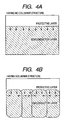
- an oxidation speed increases in a region of the boundary having the low density compared to a region of the boundary having high density.
- the oxidation speed increases in the second layer, and the damaged layer is converted into a passivated layer of high resistance by being wholly oxidized.
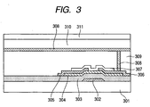
- the semiconductor layer 4 is stacked on the gate insulation layer 3.
- An oxide semiconductor containing at least one of In, Ga and Zn is used for the semiconductor layer 4.
- the structure of the semiconductor layer 4 will be described later.
- the source electrode 5 and the drain electrode 6 are stacked on the semiconductor layer 4.
- the source electrode 5 and the drain electrode 6 can employ a metal and an electroconductive oxide similar to those of the gate electrode 2.
- a film of amorphous SiO x of 100 nm is formed thereon with the sputtering technique which uses SiO 2 as the target, and is formed into a protective layer 7.
- the film for the protective layer is formed in an oxidative atmosphere by using a mixture gas of oxygen and Ar gas mixed with a ratio of 50% as a sputtering gas.
Landscapes
- Thin Film Transistor (AREA)
- Liquid Crystal (AREA)
- Electroluminescent Light Sources (AREA)
- Devices For Indicating Variable Information By Combining Individual Elements (AREA)
Applications Claiming Priority (3)
| Application Number | Priority Date | Filing Date | Title |
|---|---|---|---|
| JP2007254364 | 2007-09-28 | ||
| JP2008196038A JP4759598B2 (ja) | 2007-09-28 | 2008-07-30 | 薄膜トランジスタ、その製造方法及びそれを用いた表示装置 |
| PCT/JP2008/067363 WO2009041544A1 (en) | 2007-09-28 | 2008-09-18 | Thin film transistor, manufacturing method therefor, and display apparatus using the same |
Publications (2)
| Publication Number | Publication Date |
|---|---|
| EP2195848A1 EP2195848A1 (en) | 2010-06-16 |
| EP2195848B1 true EP2195848B1 (en) | 2012-07-18 |
Family
ID=40702613
Family Applications (1)
| Application Number | Title | Priority Date | Filing Date |
|---|---|---|---|
| EP08833155A Not-in-force EP2195848B1 (en) | 2007-09-28 | 2008-09-18 | Thin film transistor, manufacturing method therefor, and display apparatus using the same |
Country Status (7)
| Country | Link |
|---|---|
| US (2) | US8563977B2 (https=) |
| EP (1) | EP2195848B1 (https=) |
| JP (2) | JP4759598B2 (https=) |
| KR (1) | KR101148718B1 (https=) |
| CN (1) | CN101809747B (https=) |
| TW (1) | TWI377683B (https=) |
| WO (1) | WO2009041544A1 (https=) |
Families Citing this family (88)
| Publication number | Priority date | Publication date | Assignee | Title |
|---|---|---|---|---|
| JP4759598B2 (ja) * | 2007-09-28 | 2011-08-31 | キヤノン株式会社 | 薄膜トランジスタ、その製造方法及びそれを用いた表示装置 |
| EP2256795B1 (en) * | 2009-05-29 | 2014-11-19 | Semiconductor Energy Laboratory Co., Ltd. | Manufacturing method for oxide semiconductor device |
| JP5424724B2 (ja) * | 2009-06-04 | 2014-02-26 | 富士フイルム株式会社 | 電界効果型トランジスタの製造方法、電界効果型トランジスタ、表示装置、及び電磁波検出器 |
| CN102473727B (zh) * | 2009-06-29 | 2015-04-01 | 夏普株式会社 | 氧化物半导体、薄膜晶体管阵列基板及其制造方法和显示装置 |
| KR101457837B1 (ko) | 2009-06-30 | 2014-11-05 | 가부시키가이샤 한도오따이 에네루기 켄큐쇼 | 반도체 장치 제작 방법 |
| WO2011001880A1 (en) * | 2009-06-30 | 2011-01-06 | Semiconductor Energy Laboratory Co., Ltd. | Method for manufacturing semiconductor device |
| KR20120031026A (ko) | 2009-06-30 | 2012-03-29 | 가부시키가이샤 한도오따이 에네루기 켄큐쇼 | 반도체 장치 제조 방법 |
| CN111081550A (zh) | 2009-06-30 | 2020-04-28 | 株式会社半导体能源研究所 | 用于制造半导体器件的方法及半导体器件 |
| JP5663214B2 (ja) * | 2009-07-03 | 2015-02-04 | 株式会社半導体エネルギー研究所 | 半導体装置の作製方法 |
| KR101460868B1 (ko) * | 2009-07-10 | 2014-11-11 | 가부시키가이샤 한도오따이 에네루기 켄큐쇼 | 반도체 장치 |
| SG10201403913PA (en) | 2009-07-10 | 2014-10-30 | Semiconductor Energy Lab | Method for manufacturing semiconductor device |
| US8115883B2 (en) * | 2009-08-27 | 2012-02-14 | Semiconductor Energy Laboratory Co., Ltd. | Display device and method for manufacturing the same |
| WO2011027656A1 (en) * | 2009-09-04 | 2011-03-10 | Semiconductor Energy Laboratory Co., Ltd. | Transistor and display device |
| WO2011027664A1 (en) * | 2009-09-04 | 2011-03-10 | Semiconductor Energy Laboratory Co., Ltd. | Liquid crystal display device and method for manufacturing the same |
| KR101791812B1 (ko) | 2009-09-04 | 2017-10-30 | 가부시키가이샤 한도오따이 에네루기 켄큐쇼 | 반도체 장치의 제작 방법 |
| KR101988341B1 (ko) * | 2009-09-04 | 2019-06-12 | 가부시키가이샤 한도오따이 에네루기 켄큐쇼 | 발광 장치 및 발광 장치를 제작하기 위한 방법 |
| EP3540772A1 (en) * | 2009-09-16 | 2019-09-18 | Semiconductor Energy Laboratory Co., Ltd. | Transistor and display device |
| CN102511082B (zh) * | 2009-09-16 | 2016-04-27 | 株式会社半导体能源研究所 | 半导体器件及其制造方法 |
| WO2011033911A1 (en) * | 2009-09-16 | 2011-03-24 | Semiconductor Energy Laboratory Co., Ltd. | Semiconductor device and manufacturing method thereof |
| KR20130026404A (ko) * | 2009-09-24 | 2013-03-13 | 가부시키가이샤 한도오따이 에네루기 켄큐쇼 | 반도체 장치의 제조 방법 |
| KR101342179B1 (ko) | 2009-09-24 | 2013-12-16 | 가부시키가이샤 한도오따이 에네루기 켄큐쇼 | 반도체 소자 및 그 제조 방법 |
| KR101914026B1 (ko) | 2009-09-24 | 2018-11-01 | 가부시키가이샤 한도오따이 에네루기 켄큐쇼 | 산화물 반도체막 및 반도체 장치 |
| WO2011037008A1 (en) * | 2009-09-24 | 2011-03-31 | Semiconductor Energy Laboratory Co., Ltd. | Method for manufacturing oxide semiconductor film and method for manufacturing semiconductor device |
| KR20120084751A (ko) * | 2009-10-05 | 2012-07-30 | 가부시키가이샤 한도오따이 에네루기 켄큐쇼 | 반도체 장치 및 그 제작 방법 |
| KR101376461B1 (ko) * | 2009-10-08 | 2014-03-19 | 가부시키가이샤 한도오따이 에네루기 켄큐쇼 | 산화물 반도체층 및 반도체 장치 |
| WO2011043170A1 (en) | 2009-10-09 | 2011-04-14 | Semiconductor Energy Laboratory Co., Ltd. | Semiconductor device and manufacturing method thereof |
| WO2011043206A1 (en) * | 2009-10-09 | 2011-04-14 | Semiconductor Energy Laboratory Co., Ltd. | Semiconductor device |
| WO2011043194A1 (en) | 2009-10-09 | 2011-04-14 | Semiconductor Energy Laboratory Co., Ltd. | Semiconductor device and method for manufacturing the same |
| WO2011046025A1 (en) | 2009-10-16 | 2011-04-21 | Semiconductor Energy Laboratory Co., Ltd. | Logic circuit and semiconductor device |
| KR102577885B1 (ko) * | 2009-10-16 | 2023-09-14 | 가부시키가이샤 한도오따이 에네루기 켄큐쇼 | 반도체 장치 |
| KR102142450B1 (ko) * | 2009-10-30 | 2020-08-10 | 가부시키가이샤 한도오따이 에네루기 켄큐쇼 | 반도체 장치 및 반도체 장치의 제작방법 |
| KR102066532B1 (ko) * | 2009-11-06 | 2020-01-15 | 가부시키가이샤 한도오따이 에네루기 켄큐쇼 | 반도체 장치 |
| KR20190066086A (ko) | 2009-11-06 | 2019-06-12 | 가부시키가이샤 한도오따이 에네루기 켄큐쇼 | 반도체 장치 및 그 제작 방법 |
| WO2011058865A1 (en) * | 2009-11-13 | 2011-05-19 | Semiconductor Energy Laboratory Co., Ltd. | Semiconductor devi ce |
| WO2011062043A1 (en) | 2009-11-20 | 2011-05-26 | Semiconductor Energy Laboratory Co., Ltd. | Method for manufacturing semiconductor device |
| WO2011070892A1 (en) * | 2009-12-08 | 2011-06-16 | Semiconductor Energy Laboratory Co., Ltd. | Semiconductor device and manufacturing method thereof |
| WO2011070900A1 (en) * | 2009-12-08 | 2011-06-16 | Semiconductor Energy Laboratory Co., Ltd. | Semiconductor device and manufacturing method thereof |
| JP5185357B2 (ja) | 2009-12-17 | 2013-04-17 | 株式会社半導体エネルギー研究所 | 半導体装置 |
| KR101768433B1 (ko) | 2009-12-18 | 2017-08-16 | 가부시키가이샤 한도오따이 에네루기 켄큐쇼 | 반도체 장치 제작 방법 |
| KR102111309B1 (ko) | 2009-12-25 | 2020-05-15 | 가부시키가이샤 한도오따이 에네루기 켄큐쇼 | 반도체 장치 제작 방법 |
| KR101870119B1 (ko) | 2009-12-25 | 2018-06-25 | 가부시키가이샤 한도오따이 에네루기 켄큐쇼 | 반도체 장치 |
| WO2011081000A1 (en) * | 2009-12-28 | 2011-07-07 | Semiconductor Energy Laboratory Co., Ltd. | Memory device and semiconductor device |
| WO2011081009A1 (en) * | 2009-12-28 | 2011-07-07 | Semiconductor Energy Laboratory Co., Ltd. | Method for manufacturing semiconductor device |
| WO2011089844A1 (en) | 2010-01-24 | 2011-07-28 | Semiconductor Energy Laboratory Co., Ltd. | Display device and manufacturing method thereof |
| US8879010B2 (en) | 2010-01-24 | 2014-11-04 | Semiconductor Energy Laboratory Co., Ltd. | Display device |
| KR102357474B1 (ko) | 2010-02-26 | 2022-02-08 | 가부시키가이샤 한도오따이 에네루기 켄큐쇼 | 액정 표시 장치 |
| KR101921047B1 (ko) | 2010-03-26 | 2018-11-23 | 가부시키가이샤 한도오따이 에네루기 켄큐쇼 | 반도체 장치를 제작하는 방법 |
| JP5731244B2 (ja) * | 2010-03-26 | 2015-06-10 | 株式会社半導体エネルギー研究所 | 半導体装置の作製方法 |
| KR101465192B1 (ko) | 2010-04-09 | 2014-11-25 | 가부시키가이샤 한도오따이 에네루기 켄큐쇼 | 반도체 장치 |
| WO2011132556A1 (en) | 2010-04-23 | 2011-10-27 | Semiconductor Energy Laboratory Co., Ltd. | Method for manufacturing semiconductor device |
| KR101877377B1 (ko) | 2010-04-23 | 2018-07-11 | 가부시키가이샤 한도오따이 에네루기 켄큐쇼 | 반도체 장치의 제작 방법 |
| KR101806271B1 (ko) * | 2010-05-14 | 2017-12-07 | 가부시키가이샤 한도오따이 에네루기 켄큐쇼 | 반도체 장치의 제작 방법 |
| KR101872927B1 (ko) * | 2010-05-21 | 2018-06-29 | 가부시키가이샤 한도오따이 에네루기 켄큐쇼 | 반도체 장치 |
| CN102939658B (zh) | 2010-06-01 | 2014-03-26 | 夏普株式会社 | 薄膜晶体管 |
| JP2012015491A (ja) | 2010-06-04 | 2012-01-19 | Semiconductor Energy Lab Co Ltd | 光電変換装置 |
| CN102986034A (zh) * | 2010-07-02 | 2013-03-20 | 惠普发展公司,有限责任合伙企业 | 薄膜晶体管 |
| US8450123B2 (en) * | 2010-08-27 | 2013-05-28 | Semiconductor Energy Laboratory Co., Ltd. | Oxygen diffusion evaluation method of oxide film stacked body |
| WO2012029596A1 (en) | 2010-09-03 | 2012-03-08 | Semiconductor Energy Laboratory Co., Ltd. | Method for manufacturing semiconductor device |
| WO2012029612A1 (en) * | 2010-09-03 | 2012-03-08 | Semiconductor Energy Laboratory Co., Ltd. | Sputtering target and method for manufacturing semiconductor device |
| JP5969745B2 (ja) * | 2010-09-10 | 2016-08-17 | 株式会社半導体エネルギー研究所 | 半導体装置 |
| US8936965B2 (en) * | 2010-11-26 | 2015-01-20 | Semiconductor Energy Laboratory Co., Ltd. | Semiconductor device and manufacturing method thereof |
| US8823092B2 (en) | 2010-11-30 | 2014-09-02 | Semiconductor Energy Laboratory Co., Ltd. | Semiconductor device and manufacturing method thereof |
| JP2012146956A (ja) * | 2010-12-20 | 2012-08-02 | Canon Inc | チャネルエッチ型薄膜トランジスタとその製造方法 |
| CN103270601B (zh) * | 2010-12-20 | 2016-02-24 | 夏普株式会社 | 半导体装置和显示装置 |
| JP5186611B2 (ja) * | 2010-12-28 | 2013-04-17 | 出光興産株式会社 | 酸化物半導体薄膜層を有する積層構造、積層構造の製造方法、薄膜トランジスタ及び表示装置 |
| JP5189674B2 (ja) * | 2010-12-28 | 2013-04-24 | 出光興産株式会社 | 酸化物半導体薄膜層を有する積層構造、積層構造の製造方法、薄膜トランジスタ及び表示装置 |
| WO2012124511A1 (ja) * | 2011-03-11 | 2012-09-20 | シャープ株式会社 | 薄膜トランジスタおよびその製造方法、並びに表示装置 |
| WO2013047631A1 (en) * | 2011-09-29 | 2013-04-04 | Semiconductor Energy Laboratory Co., Ltd. | Semiconductor device |
| KR101942980B1 (ko) | 2012-01-17 | 2019-01-29 | 삼성디스플레이 주식회사 | 반도체 디바이스 및 그 형성 방법 |
| JP5824536B2 (ja) * | 2012-01-31 | 2015-11-25 | シャープ株式会社 | 半導体装置およびその製造方法 |
| CN104094409B (zh) * | 2012-01-31 | 2016-11-16 | 夏普株式会社 | 半导体装置及其制造方法 |
| TWI562361B (en) | 2012-02-02 | 2016-12-11 | Semiconductor Energy Lab Co Ltd | Semiconductor device |
| TWI445181B (zh) * | 2012-02-08 | 2014-07-11 | E Ink Holdings Inc | 薄膜電晶體 |
| CN103296064A (zh) * | 2012-02-29 | 2013-09-11 | 鸿富锦精密工业(深圳)有限公司 | 薄膜晶体管 |
| US9553201B2 (en) | 2012-04-02 | 2017-01-24 | Samsung Display Co., Ltd. | Thin film transistor, thin film transistor array panel, and manufacturing method of thin film transistor |
| KR20130111874A (ko) | 2012-04-02 | 2013-10-11 | 삼성디스플레이 주식회사 | 박막 트랜지스터, 이를 포함하는 박막 트랜지스터 표시판 및 표시 장치, 그리고 박막 트랜지스터의 제조 방법 |
| JP5722293B2 (ja) * | 2012-10-19 | 2015-05-20 | 株式会社神戸製鋼所 | 薄膜トランジスタ |
| JPWO2014125820A1 (ja) * | 2013-02-13 | 2017-02-02 | 出光興産株式会社 | 薄膜トランジスタ |
| KR102244553B1 (ko) * | 2013-08-23 | 2021-04-23 | 가부시키가이샤 한도오따이 에네루기 켄큐쇼 | 용량 소자 및 반도체 장치 |
| TWI566413B (zh) * | 2013-09-09 | 2017-01-11 | 元太科技工業股份有限公司 | 薄膜電晶體 |
| WO2015059850A1 (ja) * | 2013-10-24 | 2015-04-30 | 株式会社Joled | 薄膜トランジスタの製造方法 |
| WO2015186354A1 (ja) * | 2014-06-03 | 2015-12-10 | 株式会社Joled | 薄膜トランジスタ及びその製造方法 |
| JP5940124B2 (ja) * | 2014-09-04 | 2016-06-29 | 株式会社半導体エネルギー研究所 | トランジスタの作製方法 |
| CN106796959A (zh) | 2014-10-08 | 2017-05-31 | 夏普株式会社 | 半导体装置及其制造方法 |
| CN105870201B (zh) * | 2016-06-08 | 2019-01-22 | 深圳市华星光电技术有限公司 | Tft器件结构及其制作方法 |
| KR102458660B1 (ko) | 2016-08-03 | 2022-10-26 | 가부시키가이샤 한도오따이 에네루기 켄큐쇼 | 표시 장치 및 전자 기기 |
| CN106374044B (zh) * | 2016-11-02 | 2019-06-11 | 杭州潮盛科技有限公司 | 半导体结构及其制备方法 |
| CN109346412B (zh) * | 2018-09-30 | 2022-05-06 | 南京京东方显示技术有限公司 | 一种薄膜晶体管的制造方法及薄膜晶体管 |
Family Cites Families (26)
| Publication number | Priority date | Publication date | Assignee | Title |
|---|---|---|---|---|
| JPH05299657A (ja) | 1992-04-13 | 1993-11-12 | Nec Corp | 電界効果型薄膜トランジスタ素子 |
| JPH0758336A (ja) * | 1993-08-19 | 1995-03-03 | Toshiba Corp | 薄膜トランジスタ及びその製造方法 |
| JP3788021B2 (ja) * | 1998-03-30 | 2006-06-21 | セイコーエプソン株式会社 | 薄膜トランジスタおよびその製造方法 |
| DE10041699A1 (de) * | 2000-08-24 | 2002-03-21 | Infineon Technologies Ag | Niedertemperatur-Prozessierung ferroelektrischer Strontium-Wismuth-Tantalat-Schichten und Herstellung ferroelektrischer Bauelemente daraus |
| US7189992B2 (en) * | 2002-05-21 | 2007-03-13 | State Of Oregon Acting By And Through The Oregon State Board Of Higher Education On Behalf Of Oregon State University | Transistor structures having a transparent channel |
| US7541614B2 (en) * | 2003-03-11 | 2009-06-02 | Semiconductor Energy Laboratory Co., Ltd. | Integrated circuit, semiconductor device comprising the same, electronic device having the same, and driving method of the same |
| JP4108633B2 (ja) * | 2003-06-20 | 2008-06-25 | シャープ株式会社 | 薄膜トランジスタおよびその製造方法ならびに電子デバイス |
| US7262463B2 (en) * | 2003-07-25 | 2007-08-28 | Hewlett-Packard Development Company, L.P. | Transistor including a deposited channel region having a doped portion |
| US7297977B2 (en) * | 2004-03-12 | 2007-11-20 | Hewlett-Packard Development Company, L.P. | Semiconductor device |
| US7282782B2 (en) * | 2004-03-12 | 2007-10-16 | Hewlett-Packard Development Company, L.P. | Combined binary oxide semiconductor device |
| US7242039B2 (en) * | 2004-03-12 | 2007-07-10 | Hewlett-Packard Development Company, L.P. | Semiconductor device |
| US7145174B2 (en) * | 2004-03-12 | 2006-12-05 | Hewlett-Packard Development Company, Lp. | Semiconductor device |
| EP1737044B1 (en) * | 2004-03-12 | 2014-12-10 | Japan Science and Technology Agency | Amorphous oxide and thin film transistor |
| KR100998527B1 (ko) | 2004-11-10 | 2010-12-07 | 고쿠리츠다이가쿠호진 토쿄고교 다이가꾸 | 비정질 산화물 및 전계 효과 트랜지스터 |
| US7829444B2 (en) * | 2004-11-10 | 2010-11-09 | Canon Kabushiki Kaisha | Field effect transistor manufacturing method |
| JP5171003B2 (ja) * | 2005-01-28 | 2013-03-27 | 株式会社半導体エネルギー研究所 | 半導体装置 |
| JP4870404B2 (ja) * | 2005-09-02 | 2012-02-08 | 財団法人高知県産業振興センター | 薄膜トランジスタの製法 |
| JP2007073705A (ja) * | 2005-09-06 | 2007-03-22 | Canon Inc | 酸化物半導体チャネル薄膜トランジスタおよびその製造方法 |
| JP5015473B2 (ja) * | 2006-02-15 | 2012-08-29 | 財団法人高知県産業振興センター | 薄膜トランジスタアレイ及びその製法 |
| JP4609797B2 (ja) * | 2006-08-09 | 2011-01-12 | Nec液晶テクノロジー株式会社 | 薄膜デバイス及びその製造方法 |
| KR101410926B1 (ko) * | 2007-02-16 | 2014-06-24 | 삼성전자주식회사 | 박막 트랜지스터 및 그 제조방법 |
| JP5121254B2 (ja) | 2007-02-28 | 2013-01-16 | キヤノン株式会社 | 薄膜トランジスタおよび表示装置 |
| JP4759598B2 (ja) * | 2007-09-28 | 2011-08-31 | キヤノン株式会社 | 薄膜トランジスタ、その製造方法及びそれを用いた表示装置 |
| US20090090915A1 (en) * | 2007-10-05 | 2009-04-09 | Semiconductor Energy Laboratory Co., Ltd. | Thin film transistor, display device having thin film transistor, and method for manufacturing the same |
| JP5202630B2 (ja) * | 2008-06-10 | 2013-06-05 | Jx日鉱日石金属株式会社 | スパッタリング用酸化物焼結体ターゲット及びその製造方法 |
| US7977868B2 (en) * | 2008-07-23 | 2011-07-12 | Cbrite Inc. | Active matrix organic light emitting device with MO TFT backplane |
-
2008
- 2008-07-30 JP JP2008196038A patent/JP4759598B2/ja not_active Expired - Fee Related
- 2008-09-18 KR KR1020107008596A patent/KR101148718B1/ko not_active Expired - Fee Related
- 2008-09-18 WO PCT/JP2008/067363 patent/WO2009041544A1/en not_active Ceased
- 2008-09-18 EP EP08833155A patent/EP2195848B1/en not_active Not-in-force
- 2008-09-18 CN CN2008801082923A patent/CN101809747B/zh not_active Expired - Fee Related
- 2008-09-18 US US12/672,103 patent/US8563977B2/en not_active Expired - Fee Related
- 2008-09-25 TW TW097136880A patent/TWI377683B/zh not_active IP Right Cessation
-
2011
- 2011-02-17 JP JP2011031543A patent/JP5395825B2/ja not_active Expired - Fee Related
-
2012
- 2012-02-09 US US13/369,406 patent/US20120132911A1/en not_active Abandoned
Also Published As
| Publication number | Publication date |
|---|---|
| JP5395825B2 (ja) | 2014-01-22 |
| JP2009099944A (ja) | 2009-05-07 |
| KR101148718B1 (ko) | 2012-05-21 |
| TWI377683B (en) | 2012-11-21 |
| CN101809747A (zh) | 2010-08-18 |
| JP4759598B2 (ja) | 2011-08-31 |
| TW200929546A (en) | 2009-07-01 |
| US8563977B2 (en) | 2013-10-22 |
| KR20100061559A (ko) | 2010-06-07 |
| EP2195848A1 (en) | 2010-06-16 |
| US20120132911A1 (en) | 2012-05-31 |
| US20100213459A1 (en) | 2010-08-26 |
| WO2009041544A1 (en) | 2009-04-02 |
| CN101809747B (zh) | 2012-12-26 |
| JP2011146724A (ja) | 2011-07-28 |
Similar Documents
| Publication | Publication Date | Title |
|---|---|---|
| EP2195848B1 (en) | Thin film transistor, manufacturing method therefor, and display apparatus using the same | |
| US9324882B2 (en) | Thin film transistor | |
| US9024322B2 (en) | Wiring structure and display device | |
| JP6043244B2 (ja) | 薄膜トランジスタ | |
| JP5723262B2 (ja) | 薄膜トランジスタおよびスパッタリングターゲット | |
| US9412623B2 (en) | Metal oxide TFT with improved source/drain contacts and reliability | |
| US8853683B2 (en) | Semiconductor device, measurement apparatus, and measurement method of relative permittivity | |
| JP6311899B2 (ja) | 薄膜トランジスタ基板及びその製造方法 | |
| CN101884110A (zh) | 氧化物半导体薄膜晶体管 | |
| TW201005950A (en) | Thin film transistor and method of manufacturing the same | |
| KR20110128038A (ko) | 산화물 반도체 박막 트랜지스터 | |
| US10396187B2 (en) | Semiconductor device | |
| JP2015149467A (ja) | 薄膜トランジスタ基板の製造方法 | |
| US20140167047A1 (en) | Metal oxide tft with improved temperature stability | |
| CN109755136A (zh) | 薄膜晶体管的制造方法和薄膜晶体管 | |
| US20250040191A1 (en) | Engineering metal oxide layer interfaces to improve electronic device stability | |
| WO2010061554A1 (ja) | トランジスタ及びその製造方法 | |
| US20250294807A1 (en) | Double gated thin film transistor integration |
Legal Events
| Date | Code | Title | Description |
|---|---|---|---|
| PUAI | Public reference made under article 153(3) epc to a published international application that has entered the european phase |
Free format text: ORIGINAL CODE: 0009012 |
|
| 17P | Request for examination filed |
Effective date: 20100324 |
|
| AK | Designated contracting states |
Kind code of ref document: A1 Designated state(s): AT BE BG CH CY CZ DE DK EE ES FI FR GB GR HR HU IE IS IT LI LT LU LV MC MT NL NO PL PT RO SE SI SK TR |
|
| AX | Request for extension of the european patent |
Extension state: AL BA MK RS |
|
| DAX | Request for extension of the european patent (deleted) | ||
| REG | Reference to a national code |
Ref country code: DE Ref legal event code: R079 Ref document number: 602008017308 Country of ref document: DE Free format text: PREVIOUS MAIN CLASS: H01L0029786000 Ipc: H01L0021336000 |
|
| RIC1 | Information provided on ipc code assigned before grant |
Ipc: H01L 29/786 20060101ALI20111121BHEP Ipc: H01L 21/336 20060101AFI20111121BHEP |
|
| GRAP | Despatch of communication of intention to grant a patent |
Free format text: ORIGINAL CODE: EPIDOSNIGR1 |
|
| GRAS | Grant fee paid |
Free format text: ORIGINAL CODE: EPIDOSNIGR3 |
|
| GRAA | (expected) grant |
Free format text: ORIGINAL CODE: 0009210 |
|
| AK | Designated contracting states |
Kind code of ref document: B1 Designated state(s): AT BE BG CH CY CZ DE DK EE ES FI FR GB GR HR HU IE IS IT LI LT LU LV MC MT NL NO PL PT RO SE SI SK TR |
|
| REG | Reference to a national code |
Ref country code: GB Ref legal event code: FG4D |
|
| REG | Reference to a national code |
Ref country code: CH Ref legal event code: EP |
|
| REG | Reference to a national code |
Ref country code: AT Ref legal event code: REF Ref document number: 567207 Country of ref document: AT Kind code of ref document: T Effective date: 20120815 Ref country code: IE Ref legal event code: FG4D |
|
| REG | Reference to a national code |
Ref country code: DE Ref legal event code: R096 Ref document number: 602008017308 Country of ref document: DE Effective date: 20120913 |
|
| REG | Reference to a national code |
Ref country code: NL Ref legal event code: VDEP Effective date: 20120718 |
|
| REG | Reference to a national code |
Ref country code: AT Ref legal event code: MK05 Ref document number: 567207 Country of ref document: AT Kind code of ref document: T Effective date: 20120718 |
|
| REG | Reference to a national code |
Ref country code: LT Ref legal event code: MG4D Effective date: 20120718 |
|
| PG25 | Lapsed in a contracting state [announced via postgrant information from national office to epo] |
Ref country code: CY Free format text: LAPSE BECAUSE OF FAILURE TO SUBMIT A TRANSLATION OF THE DESCRIPTION OR TO PAY THE FEE WITHIN THE PRESCRIBED TIME-LIMIT Effective date: 20120718 Ref country code: HR Free format text: LAPSE BECAUSE OF FAILURE TO SUBMIT A TRANSLATION OF THE DESCRIPTION OR TO PAY THE FEE WITHIN THE PRESCRIBED TIME-LIMIT Effective date: 20120718 Ref country code: FI Free format text: LAPSE BECAUSE OF FAILURE TO SUBMIT A TRANSLATION OF THE DESCRIPTION OR TO PAY THE FEE WITHIN THE PRESCRIBED TIME-LIMIT Effective date: 20120718 Ref country code: AT Free format text: LAPSE BECAUSE OF FAILURE TO SUBMIT A TRANSLATION OF THE DESCRIPTION OR TO PAY THE FEE WITHIN THE PRESCRIBED TIME-LIMIT Effective date: 20120718 Ref country code: BE Free format text: LAPSE BECAUSE OF FAILURE TO SUBMIT A TRANSLATION OF THE DESCRIPTION OR TO PAY THE FEE WITHIN THE PRESCRIBED TIME-LIMIT Effective date: 20120718 Ref country code: IS Free format text: LAPSE BECAUSE OF FAILURE TO SUBMIT A TRANSLATION OF THE DESCRIPTION OR TO PAY THE FEE WITHIN THE PRESCRIBED TIME-LIMIT Effective date: 20121118 Ref country code: LT Free format text: LAPSE BECAUSE OF FAILURE TO SUBMIT A TRANSLATION OF THE DESCRIPTION OR TO PAY THE FEE WITHIN THE PRESCRIBED TIME-LIMIT Effective date: 20120718 Ref country code: NO Free format text: LAPSE BECAUSE OF FAILURE TO SUBMIT A TRANSLATION OF THE DESCRIPTION OR TO PAY THE FEE WITHIN THE PRESCRIBED TIME-LIMIT Effective date: 20121018 |
|
| PG25 | Lapsed in a contracting state [announced via postgrant information from national office to epo] |
Ref country code: SE Free format text: LAPSE BECAUSE OF FAILURE TO SUBMIT A TRANSLATION OF THE DESCRIPTION OR TO PAY THE FEE WITHIN THE PRESCRIBED TIME-LIMIT Effective date: 20120718 Ref country code: SI Free format text: LAPSE BECAUSE OF FAILURE TO SUBMIT A TRANSLATION OF THE DESCRIPTION OR TO PAY THE FEE WITHIN THE PRESCRIBED TIME-LIMIT Effective date: 20120718 Ref country code: LV Free format text: LAPSE BECAUSE OF FAILURE TO SUBMIT A TRANSLATION OF THE DESCRIPTION OR TO PAY THE FEE WITHIN THE PRESCRIBED TIME-LIMIT Effective date: 20120718 Ref country code: PL Free format text: LAPSE BECAUSE OF FAILURE TO SUBMIT A TRANSLATION OF THE DESCRIPTION OR TO PAY THE FEE WITHIN THE PRESCRIBED TIME-LIMIT Effective date: 20120718 Ref country code: GR Free format text: LAPSE BECAUSE OF FAILURE TO SUBMIT A TRANSLATION OF THE DESCRIPTION OR TO PAY THE FEE WITHIN THE PRESCRIBED TIME-LIMIT Effective date: 20121019 Ref country code: PT Free format text: LAPSE BECAUSE OF FAILURE TO SUBMIT A TRANSLATION OF THE DESCRIPTION OR TO PAY THE FEE WITHIN THE PRESCRIBED TIME-LIMIT Effective date: 20121119 |
|
| PG25 | Lapsed in a contracting state [announced via postgrant information from national office to epo] |
Ref country code: NL Free format text: LAPSE BECAUSE OF FAILURE TO SUBMIT A TRANSLATION OF THE DESCRIPTION OR TO PAY THE FEE WITHIN THE PRESCRIBED TIME-LIMIT Effective date: 20120718 |
|
| PG25 | Lapsed in a contracting state [announced via postgrant information from national office to epo] |
Ref country code: DK Free format text: LAPSE BECAUSE OF FAILURE TO SUBMIT A TRANSLATION OF THE DESCRIPTION OR TO PAY THE FEE WITHIN THE PRESCRIBED TIME-LIMIT Effective date: 20120718 Ref country code: CZ Free format text: LAPSE BECAUSE OF FAILURE TO SUBMIT A TRANSLATION OF THE DESCRIPTION OR TO PAY THE FEE WITHIN THE PRESCRIBED TIME-LIMIT Effective date: 20120718 Ref country code: EE Free format text: LAPSE BECAUSE OF FAILURE TO SUBMIT A TRANSLATION OF THE DESCRIPTION OR TO PAY THE FEE WITHIN THE PRESCRIBED TIME-LIMIT Effective date: 20120718 Ref country code: RO Free format text: LAPSE BECAUSE OF FAILURE TO SUBMIT A TRANSLATION OF THE DESCRIPTION OR TO PAY THE FEE WITHIN THE PRESCRIBED TIME-LIMIT Effective date: 20120718 Ref country code: ES Free format text: LAPSE BECAUSE OF FAILURE TO SUBMIT A TRANSLATION OF THE DESCRIPTION OR TO PAY THE FEE WITHIN THE PRESCRIBED TIME-LIMIT Effective date: 20121029 Ref country code: MC Free format text: LAPSE BECAUSE OF NON-PAYMENT OF DUE FEES Effective date: 20120930 |
|
| REG | Reference to a national code |
Ref country code: CH Ref legal event code: PL |
|
| PLBE | No opposition filed within time limit |
Free format text: ORIGINAL CODE: 0009261 |
|
| STAA | Information on the status of an ep patent application or granted ep patent |
Free format text: STATUS: NO OPPOSITION FILED WITHIN TIME LIMIT |
|
| PG25 | Lapsed in a contracting state [announced via postgrant information from national office to epo] |
Ref country code: SK Free format text: LAPSE BECAUSE OF FAILURE TO SUBMIT A TRANSLATION OF THE DESCRIPTION OR TO PAY THE FEE WITHIN THE PRESCRIBED TIME-LIMIT Effective date: 20120718 Ref country code: IT Free format text: LAPSE BECAUSE OF FAILURE TO SUBMIT A TRANSLATION OF THE DESCRIPTION OR TO PAY THE FEE WITHIN THE PRESCRIBED TIME-LIMIT Effective date: 20120718 |
|
| REG | Reference to a national code |
Ref country code: IE Ref legal event code: MM4A |
|
| 26N | No opposition filed |
Effective date: 20130419 |
|
| REG | Reference to a national code |
Ref country code: FR Ref legal event code: ST Effective date: 20130531 |
|
| PG25 | Lapsed in a contracting state [announced via postgrant information from national office to epo] |
Ref country code: CH Free format text: LAPSE BECAUSE OF NON-PAYMENT OF DUE FEES Effective date: 20120930 Ref country code: LI Free format text: LAPSE BECAUSE OF NON-PAYMENT OF DUE FEES Effective date: 20120930 Ref country code: IE Free format text: LAPSE BECAUSE OF NON-PAYMENT OF DUE FEES Effective date: 20120918 Ref country code: BG Free format text: LAPSE BECAUSE OF FAILURE TO SUBMIT A TRANSLATION OF THE DESCRIPTION OR TO PAY THE FEE WITHIN THE PRESCRIBED TIME-LIMIT Effective date: 20121018 |
|
| REG | Reference to a national code |
Ref country code: DE Ref legal event code: R097 Ref document number: 602008017308 Country of ref document: DE Effective date: 20130419 |
|
| PG25 | Lapsed in a contracting state [announced via postgrant information from national office to epo] |
Ref country code: FR Free format text: LAPSE BECAUSE OF NON-PAYMENT OF DUE FEES Effective date: 20121001 |
|
| PG25 | Lapsed in a contracting state [announced via postgrant information from national office to epo] |
Ref country code: MT Free format text: LAPSE BECAUSE OF FAILURE TO SUBMIT A TRANSLATION OF THE DESCRIPTION OR TO PAY THE FEE WITHIN THE PRESCRIBED TIME-LIMIT Effective date: 20120718 |
|
| PG25 | Lapsed in a contracting state [announced via postgrant information from national office to epo] |
Ref country code: TR Free format text: LAPSE BECAUSE OF FAILURE TO SUBMIT A TRANSLATION OF THE DESCRIPTION OR TO PAY THE FEE WITHIN THE PRESCRIBED TIME-LIMIT Effective date: 20120718 |
|
| PG25 | Lapsed in a contracting state [announced via postgrant information from national office to epo] |
Ref country code: LU Free format text: LAPSE BECAUSE OF NON-PAYMENT OF DUE FEES Effective date: 20120918 |
|
| PG25 | Lapsed in a contracting state [announced via postgrant information from national office to epo] |
Ref country code: HU Free format text: LAPSE BECAUSE OF FAILURE TO SUBMIT A TRANSLATION OF THE DESCRIPTION OR TO PAY THE FEE WITHIN THE PRESCRIBED TIME-LIMIT Effective date: 20080918 |
|
| PGFP | Annual fee paid to national office [announced via postgrant information from national office to epo] |
Ref country code: GB Payment date: 20170929 Year of fee payment: 10 |
|
| PGFP | Annual fee paid to national office [announced via postgrant information from national office to epo] |
Ref country code: DE Payment date: 20171130 Year of fee payment: 10 |
|
| REG | Reference to a national code |
Ref country code: DE Ref legal event code: R119 Ref document number: 602008017308 Country of ref document: DE |
|
| GBPC | Gb: european patent ceased through non-payment of renewal fee |
Effective date: 20180918 |
|
| PG25 | Lapsed in a contracting state [announced via postgrant information from national office to epo] |
Ref country code: DE Free format text: LAPSE BECAUSE OF NON-PAYMENT OF DUE FEES Effective date: 20190402 |
|
| PG25 | Lapsed in a contracting state [announced via postgrant information from national office to epo] |
Ref country code: GB Free format text: LAPSE BECAUSE OF NON-PAYMENT OF DUE FEES Effective date: 20180918 |