EP2186004B1 - Halbleiterspeicherbauelement und verfahren zu seiner steuerung - Google Patents
Halbleiterspeicherbauelement und verfahren zu seiner steuerung Download PDFInfo
- Publication number
- EP2186004B1 EP2186004B1 EP08791594.8A EP08791594A EP2186004B1 EP 2186004 B1 EP2186004 B1 EP 2186004B1 EP 08791594 A EP08791594 A EP 08791594A EP 2186004 B1 EP2186004 B1 EP 2186004B1
- Authority
- EP
- European Patent Office
- Prior art keywords
- error
- data
- correcting
- corrected
- errors
- Prior art date
- Legal status (The legal status is an assumption and is not a legal conclusion. Google has not performed a legal analysis and makes no representation as to the accuracy of the status listed.)
- Not-in-force
Links
Images


Classifications
-
- G—PHYSICS
- G06—COMPUTING OR CALCULATING; COUNTING
- G06F—ELECTRIC DIGITAL DATA PROCESSING
- G06F11/00—Error detection; Error correction; Monitoring
- G06F11/07—Responding to the occurrence of a fault, e.g. fault tolerance
- G06F11/08—Error detection or correction by redundancy in data representation, e.g. by using checking codes
- G06F11/10—Adding special bits or symbols to the coded information, e.g. parity check, casting out 9's or 11's
-
- H—ELECTRICITY
- H03—ELECTRONIC CIRCUITRY
- H03M—CODING; DECODING; CODE CONVERSION IN GENERAL
- H03M13/00—Coding, decoding or code conversion, for error detection or error correction; Coding theory basic assumptions; Coding bounds; Error probability evaluation methods; Channel models; Simulation or testing of codes
- H03M13/29—Coding, decoding or code conversion, for error detection or error correction; Coding theory basic assumptions; Coding bounds; Error probability evaluation methods; Channel models; Simulation or testing of codes combining two or more codes or code structures, e.g. product codes, generalised product codes, concatenated codes, inner and outer codes
- H03M13/2906—Coding, decoding or code conversion, for error detection or error correction; Coding theory basic assumptions; Coding bounds; Error probability evaluation methods; Channel models; Simulation or testing of codes combining two or more codes or code structures, e.g. product codes, generalised product codes, concatenated codes, inner and outer codes using block codes
-
- G—PHYSICS
- G06—COMPUTING OR CALCULATING; COUNTING
- G06F—ELECTRIC DIGITAL DATA PROCESSING
- G06F11/00—Error detection; Error correction; Monitoring
- G06F11/07—Responding to the occurrence of a fault, e.g. fault tolerance
- G06F11/08—Error detection or correction by redundancy in data representation, e.g. by using checking codes
- G06F11/10—Adding special bits or symbols to the coded information, e.g. parity check, casting out 9's or 11's
- G06F11/1008—Adding special bits or symbols to the coded information, e.g. parity check, casting out 9's or 11's in individual solid state devices
- G06F11/1012—Adding special bits or symbols to the coded information, e.g. parity check, casting out 9's or 11's in individual solid state devices using codes or arrangements adapted for a specific type of error
-
- G—PHYSICS
- G06—COMPUTING OR CALCULATING; COUNTING
- G06F—ELECTRIC DIGITAL DATA PROCESSING
- G06F11/00—Error detection; Error correction; Monitoring
- G06F11/07—Responding to the occurrence of a fault, e.g. fault tolerance
- G06F11/08—Error detection or correction by redundancy in data representation, e.g. by using checking codes
- G06F11/10—Adding special bits or symbols to the coded information, e.g. parity check, casting out 9's or 11's
- G06F11/1004—Adding special bits or symbols to the coded information, e.g. parity check, casting out 9's or 11's to protect a block of data words, e.g. CRC or checksum
-
- G—PHYSICS
- G06—COMPUTING OR CALCULATING; COUNTING
- G06F—ELECTRIC DIGITAL DATA PROCESSING
- G06F11/00—Error detection; Error correction; Monitoring
- G06F11/07—Responding to the occurrence of a fault, e.g. fault tolerance
- G06F11/08—Error detection or correction by redundancy in data representation, e.g. by using checking codes
- G06F11/10—Adding special bits or symbols to the coded information, e.g. parity check, casting out 9's or 11's
- G06F11/1008—Adding special bits or symbols to the coded information, e.g. parity check, casting out 9's or 11's in individual solid state devices
- G06F11/1068—Adding special bits or symbols to the coded information, e.g. parity check, casting out 9's or 11's in individual solid state devices in sector programmable memories, e.g. flash disk
-
- G—PHYSICS
- G06—COMPUTING OR CALCULATING; COUNTING
- G06F—ELECTRIC DIGITAL DATA PROCESSING
- G06F13/00—Interconnection of, or transfer of information or other signals between, memories, input/output devices or central processing units
- G06F13/14—Handling requests for interconnection or transfer
- G06F13/16—Handling requests for interconnection or transfer for access to memory bus
- G06F13/1668—Details of memory controller
- G06F13/1673—Details of memory controller using buffers
-
- G—PHYSICS
- G06—COMPUTING OR CALCULATING; COUNTING
- G06F—ELECTRIC DIGITAL DATA PROCESSING
- G06F13/00—Interconnection of, or transfer of information or other signals between, memories, input/output devices or central processing units
- G06F13/38—Information transfer, e.g. on bus
- G06F13/40—Bus structure
- G06F13/4063—Device-to-bus coupling
- G06F13/4068—Electrical coupling
-
- G—PHYSICS
- G11—INFORMATION STORAGE
- G11C—STATIC STORES
- G11C29/00—Checking stores for correct operation ; Subsequent repair; Testing stores during standby or offline operation
- G11C29/52—Protection of memory contents; Detection of errors in memory contents
-
- H—ELECTRICITY
- H03—ELECTRONIC CIRCUITRY
- H03M—CODING; DECODING; CODE CONVERSION IN GENERAL
- H03M13/00—Coding, decoding or code conversion, for error detection or error correction; Coding theory basic assumptions; Coding bounds; Error probability evaluation methods; Channel models; Simulation or testing of codes
- H03M13/29—Coding, decoding or code conversion, for error detection or error correction; Coding theory basic assumptions; Coding bounds; Error probability evaluation methods; Channel models; Simulation or testing of codes combining two or more codes or code structures, e.g. product codes, generalised product codes, concatenated codes, inner and outer codes
-
- H—ELECTRICITY
- H03—ELECTRONIC CIRCUITRY
- H03M—CODING; DECODING; CODE CONVERSION IN GENERAL
- H03M13/00—Coding, decoding or code conversion, for error detection or error correction; Coding theory basic assumptions; Coding bounds; Error probability evaluation methods; Channel models; Simulation or testing of codes
- H03M13/35—Unequal or adaptive error protection, e.g. by providing a different level of protection according to significance of source information or by adapting the coding according to the change of transmission channel characteristics
-
- H—ELECTRICITY
- H03—ELECTRONIC CIRCUITRY
- H03M—CODING; DECODING; CODE CONVERSION IN GENERAL
- H03M13/00—Coding, decoding or code conversion, for error detection or error correction; Coding theory basic assumptions; Coding bounds; Error probability evaluation methods; Channel models; Simulation or testing of codes
- H03M13/65—Purpose and implementation aspects
- H03M13/6561—Parallelized implementations
-
- H—ELECTRICITY
- H03—ELECTRONIC CIRCUITRY
- H03M—CODING; DECODING; CODE CONVERSION IN GENERAL
- H03M13/00—Coding, decoding or code conversion, for error detection or error correction; Coding theory basic assumptions; Coding bounds; Error probability evaluation methods; Channel models; Simulation or testing of codes
- H03M13/03—Error detection or forward error correction by redundancy in data representation, i.e. code words containing more digits than the source words
-
- Y—GENERAL TAGGING OF NEW TECHNOLOGICAL DEVELOPMENTS; GENERAL TAGGING OF CROSS-SECTIONAL TECHNOLOGIES SPANNING OVER SEVERAL SECTIONS OF THE IPC; TECHNICAL SUBJECTS COVERED BY FORMER USPC CROSS-REFERENCE ART COLLECTIONS [XRACs] AND DIGESTS
- Y02—TECHNOLOGIES OR APPLICATIONS FOR MITIGATION OR ADAPTATION AGAINST CLIMATE CHANGE
- Y02D—CLIMATE CHANGE MITIGATION TECHNOLOGIES IN INFORMATION AND COMMUNICATION TECHNOLOGIES [ICT], I.E. INFORMATION AND COMMUNICATION TECHNOLOGIES AIMING AT THE REDUCTION OF THEIR OWN ENERGY USE
- Y02D10/00—Energy efficient computing, e.g. low power processors, power management or thermal management
Definitions
- the present invention relates to a semiconductor memory device and a method of controlling the same and, for example, to a memory device which nonvolatilely stores information and has an error correction circuit, and a method of controlling the memory device.
- nonvolatile memory devices In some kinds of nonvolatile memory devices, the state of the physical quantity that controls data storage changes along with the elapse of time. If the elapsed time has reached a predetermined length, the data may be lost.
- memory devices having such a characteristic feature.
- One of such memory devices is, e.g., a nonvolatile semiconductor memory device which uses transistors having a so-called laminated gate structure as memory cells.
- the laminated gate structure includes a tunnel insulating film, floating gate electrode, interelectrode insulating film, and control gate electrode which are sequentially stacked on a substrate.
- a tunnel insulating film To store information in a memory cell, electrons are injected from the substrate to the floating gate electrode through the tunnel insulating film. The electric charges accumulated in the floating gate electrode retain information. The electric charges accumulated in the floating gate electrode leak to the substrate through the tunnel insulating film as the time elapses. For this reason, the information retained in the memory cell can be lost along with the elapse of time (an error can occur in the information).
- a memory device having a plurality of such memory cells sometimes includes an error correction mechanism for restoring erroneous information to a correct state.
- a correction mechanism having a high error correction capability is necessary.
- a correction mechanism with a high error correction capability has a large circuit scale and requires high power consumption and a long time for processing.
- a memory device uses a correction mechanism having a high error correction capability. The high-performance error correction mechanism is applied equally regardless of the length of the elapsed time from information storage.
- the high-performance error correction mechanism is used. Since the information to be read contains not so many errors, the use of the high-performance error correction mechanism is wasteful. This leads to a waste of power in the memory device.
- an error-correcting code is generated not for 512-byte data but for, e.g., 4-kbyte data obtained by concatenating a plurality of 512-byte data. This increases the error correction capability. In this method, however, it is necessary to always read out 4-kbyte data even in reading out 512-byte data. This also results in a waste of power in the memory device.
- US2007/0157064 A1 describes systems and methods for error corrections in a NAND Flash memory, in which a plurality of error correction schemes are applied when encoding data to be stored in the memory, and depending on circumstances, at least one of the error correction schemes is selectively applied to encoded blocks of data.
- a semiconductor memory device comprising: a plurality of detecting code generators configured to generate a plurality of detecting codes to detect errors in a plurality of data items, respectively; a plurality of first correcting code generators configured to generate a plurality of first correcting codes to correct errors in a plurality of first data blocks, respectively, each of the first data blocks containing one of the data items and a corresponding detecting code; a second correcting code generator configured to generate a second correcting code to correct errors in a second data block, the second data block containing the plurality of first data blocks; and a semiconductor memory configured to nonvolatilely store the second data block, the plurality of first correcting codes, and the second correcting code, wherein the second correcting code generator (8) has an error correction capability higher than that of the plurality of first correcting code generators (61) .
- a semiconductor memory device comprising: A method of controlling a semiconductor memory device, the method comprising: generating a plurality of detecting codes to detect errors in a plurality of data items, respectively; generating a plurality of first correcting codes to correct errors in a plurality of first data block, respectively, each of the first data blocks containing one of the data
- the second correcting code generator (8) has an error correction capability higher than that of the plurality of first correcting code generators (61) .
- the functional blocks of the embodiments of the present invention can be implemented by hardware, computer software, or a combination thereof.
- the blocks will be described below generally from the viewpoint of their functions while clarifying that they can be implemented by both of hardware and software. Whether to execute a function as hardware or software depends on the specific embodiments or design restrictions on the entire system. Those skilled in the art can implement the function by various methods for each of the specific embodiments, and the present invention incorporates such implementation.
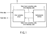
- FIG. 1 is a block diagram schematically illustrating a semiconductor memory device according to an embodiment.
- a semiconductor memory device 10 includes an error correction circuit 1 and a semiconductor memory 2.
- the error correction circuit 1 and the semiconductor memory 2 are formed as, e.g., one semiconductor integrated circuit on a single semiconductor chip.
- the semiconductor memory 2 can be any memory device if it can nonvolatilely store information, and the stored data can be changed.
- An example of the semiconductor memory 2 is a NAND flash memory.
- a NAND flash memory has a plurality of memory cells.
- Each memory cell is formed from a MOSFET (metal oxide semiconductor field effect transistor) having a so-called laminated gate structure.
- MOSFET metal oxide semiconductor field effect transistor
- a MOS transistor with the laminated gate structure includes a tunnel insulating film, floating gate electrode, interelectrode insulating film, control gate electrode, and source and drain diffusion layers.
- the threshold voltage of each memory cell transistor is changed in accordance with the amount of electric charge accumulated in the floating gate electrode, and each memory cell transistor stores information corresponding to the change in the threshold voltage.
- the memory cell transistor can be designed to store either 1-bit information or information of a plurality of bits.
- a control circuit including a sense amplifier and a potential generation circuit in the semiconductor memory 2 can write data supplied to the semiconductor memory 2 in the memory cell transistors, or output data stored in the memory cell transistor outside the semiconductor memory 2.
- the control gate electrodes of memory cell transistors belonging to the same row are connected to a single word line.
- a select gate transistor is provided at each of the ends of memory cell transistors which belong to the same column and are connected in series.
- One select gate transistor is connected to a bit line. Based on this rule, the memory cell transistors, select gate transistors, word lines, and bit lines are provided. Data write and read are done for each set of a plurality of memory cell transistors.
- a storage area formed from a set of memory cell transistors corresponds to one page.
- a plurality of pages form a block.
- the NAND flash memory erases data in each block.
- Data (write data) required to be written in the semiconductor memory 2 is externally supplied to the semiconductor memory device 10.
- the error correction circuit 1 adds an error-correcting code and an error-detecting code to the write data and supplies it to the semiconductor memory 2.
- the semiconductor memory 2 stores the write data with the error-correcting code and the error-detecting code.
- the semiconductor memory 2 supplies data (read data) required to be read, and an error-correcting code and an error-detecting code added to the read data to the error correction circuit 1.
- the error correction circuit 1 detects and corrects an error in the read data. If an error exists, the error correction circuit 1 corrects it, removes the error-correcting code and the error-detecting code, and outputs the read data to an external device.
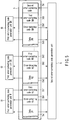
- FIG. 2 is a block diagram illustrating the main portion of the error correction circuit 1 associated with data write.
- the error correction circuit 1 generates an error-correcting code for each of a plurality of write data each having a predetermined size and also generates another error-correcting code for the set of plurality of write data.
- the number of write data is decided in accordance with the error correction capability desired to achieve and the error-correcting codes to be employed. An example in which the number of write data is 8 will be described below.
- the error correction circuit 1 receives write data items Da1 to Da8.
- the first size can match, e.g., the size of write or read data of the semiconductor memory 2. More specifically, when a NAND flash memory is used as the semiconductor memory 2, the write data size corresponds to the size of one page, which is, e.g., 512 bytes. In the following example, the first size is 512 bytes, for descriptive convenience.
- the error correction circuit 1 has a temporary storage circuit 3.
- the temporary storage circuit 3 is formed from, e.g., a volatile storage circuit and can be, e.g., a DRAM (dynamic random access memory).
- the temporary storage circuit 3 serves as a temporary storage area in write when generating an error-detecting code and an error-correcting code for write data to the semiconductor memory 2.
- the temporary storage circuit 3 receives the write data items Da1 to Da8.
- the temporary storage circuit 3 stores the write data items Da1 to Da8.
- the write data items Da1 to Da8 are supplied to error-detecting code generation units 41 to 48 (some are not illustrated), respectively.
- the error-detecting code generation units 41 to 48 generate (data of) error-detecting codes Db1 to Db8 for the write data items Da1 to Da8, respectively.
- the error-detecting codes Db1 to Db8 are used to detect errors in the write data items Da1 to Da8.
- a code that allows the error-detecting code generation units to easily calculate codes and reduce the power consumption while achieving the above-described object is used as the error-detecting codes Db1 to Db8.
- CRC Cyclic Redundancy Checksum
- CRC16 is usable as the error-detecting code.
- the error-detecting codes Db1 to Db8 are supplied to the temporary storage circuit 3.
- the error-detecting codes Db1 to Db8 are also supplied to first error-correcting code generation units 61 to 68, respectively.
- the first error-correcting code generation units 61 to 68 also receive the write data items Da1 to Da8, respectively.
- the first error-correcting code generation units 61 to 68 generate first error-correcting codes using the write data items Da1 to Da8 and the error-detecting codes Db1 to Db8.
- the first error-correcting code generated by the first error-correcting code generation unit 61 is used to correct errors in the write data item Da1 and the error-detecting code data Db1.
- the first error-correcting codes generated by the first error-correcting code generation units 62 to 68 are used to correct errors in the write data items Da2 to Da8 and the error-detecting code data Db2 to Db8.
- the first error-correcting code for example, a code which has a relatively low error correction capability of about 1 bit, requires no high power and no long time for calculation, and needs only a small scale circuit for execution is usable. More specifically, for example, a Hamming code is usable as the first error-correcting code.
- the first error-correcting code generation units 61 to 68 output (data of) first error-correcting codes Dc1 to Dc8, respectively.
- the first error-correcting codes Dc1 to Dc8 are supplied to the temporary storage circuit 3.
- the error-detecting codes Db1 to Db8 are supplied to a second error-correcting code generation unit 8.
- the second error-correcting code generation unit 8 also receives the write data items Da1 to Da8.
- the second error-correcting code generation unit 8 generates a second error-correcting code using the write data items Da1 to Da8 and the error-detecting codes Db1 to Db8.
- the second error-correcting code is used to correct errors in the write data items Da1 to Da8 and the error-detecting codes Db1 to Db8.
- the second error-correcting code for example, a code which enables error correction at a higher capability than the error correction using the first error-correcting code and can correct errors of multiple bits, although the calculation amount is large, is usable. More specifically, for example, a BHC code, Reed-Solomon (RS) code, or LDPC (Low Density Parity Check) code is usable as the second error-correcting code.
- the circuit scale, power consumption, and calculation time of the second error-correcting code generation unit 8 exceed those of the first error-correcting code generation units 61 to 68 because of the large calculation amount. However, the second error-correcting code generation unit 8 has a higher error correction capability than the first error-correcting code generation units 61 to 68.
- the second error-correcting code generation unit 8 supplies (data of) a second error-correcting code Dd to the temporary storage circuit 3.
- the temporary storage circuit 3 supplies, to the semiconductor memory 2, the write data items Da1 to Da8, error-detecting codes Db1 to Db8, first error-correcting codes Dc1 to Dc8, and second error-correcting code Dd, which have structures to be described later.
- FIGS. 3 to 6 schematically show data states in the temporary storage circuit 3 in write sequentially.
- the eight write data items Da1 to Da8 to be written in the semiconductor memory 2 are supplied to the error correction circuit 1.
- the write data items Da1 to Da8 are stored in the temporary storage circuit 3.
- the write data items Da1 to Da8 are supplied to the error-detecting code generation units 41 to 48, respectively.
- the error-detecting code generation units 41 to 48 generate the error-detecting codes Db1 to Db8 for the write data items Da1 to Da8, respectively.
- CRC32 is used as the error-detecting codes
- each of the error-detecting codes Db1 to Db8 has a size of 32 bits.
- the write data item Da1 and the error-detecting code Db1 concatenated after the write data item Da1 form first data block D1 that is a unit of error correction.
- the write data items Da2 to Da8 and the error-detecting codes Db2 to Db8 concatenated after them form first data blocks D2 to D8.
- the first data blocks D1 to D8 are stored in the temporary storage circuit 3.
- the error-detecting code generation units 41 to 48 perform the detecting code generation operations in parallel. The parallel operations of the error-detecting code generation units 41 to 48 shorten the processing time.
- the first data blocks D1 to D8 are supplied to the first error-correcting code generation units 61 to 68, respectively.
- the first error-correcting code generation unit 61 generates, using the first data block D1, the first error-correcting code Dc1 for correcting errors in the first data block D1.
- the first error-correcting code Dc1 is concatenated after the error-detecting code Db1 and before the write data item Da2 and stored in the temporary storage circuit 3.
- the first error-correcting code generation units 62 to 68 respectively generate, using the first data blocks D2 to D8, the first error-correcting codes Dc2 to Dc8 for correcting errors in the first data blocks D2 to D8.
- the first error-correcting code Dc2 is concatenated after the error-detecting code Db2 and before the write data item Da3 and stored in the temporary storage circuit 3.
- the first error-correcting codes Dc3 to Dc7 are respectively concatenated after the error-detecting codes Db3 to Db7 and before the write data items Da4 to Da8 and stored in the temporary storage circuit 3.
- the first error-correcting code Dc8 is concatenated after the error-detecting code Db8 and stored in the temporary storage circuit 3.
- each of the first data blocks D1 to D8 has a size corresponding to write data (4096 bits) + error-detecting code (32 bits).
- each of the first error-correcting codes Dc1 to Dc8 has a size of, e.g., 13 bits.
- the first error-correcting code generation units 61 to 68 perform the correcting code generation operations in parallel. The parallel operations of the first error-correcting code generation units 61 to 68 shorten the processing time.
- the first data blocks D1 to D8 are concatenated in order to form a second data block.
- the second data block is supplied to the second error-correcting code generation unit 8.
- the second data block is a unit of data to be used by the second error-correcting code generation unit to generate the second error-correcting code.
- the second error-correcting code generation unit 8 generates, using the second data block, the second error-correcting code Dd for correcting errors in the second data block.
- the second error-correcting code Dd is concatenated after the second data block and stored in the temporary storage circuit 3.
- the second data block has a size corresponding to write data (4096 bits) ⁇ 8 + error-detecting code (32 bits) ⁇ 8 and corrects a 12-bit error in the second data block.
- the second error-correcting code Dd has a size of, e.g., 192 bits.
- the second error-correcting code Dd is concatenated after the second data block in the above-described processes, thereby obtaining a transfer data block (the structure in the temporary storage circuit 3 in FIG. 5 ).
- the transfer data block is supplied to the semiconductor memory 2.
- the semiconductor memory 2 stores each transfer data block.
- FIG. 6 is a block diagram illustrating the main portion of the error correction circuit 1 associated with data read.
- the semiconductor memory 2 supplies a signal S1 to a first error correction unit 11.
- the signal S1 is formed from a transfer data block (the structure in the temporary storage circuit 3 in FIG. 5 ).
- the first error correction unit 11 corrects the errors in the first data blocks D1 to D8 using the first error-correcting codes Dc1 to Dc8 in the signal S1, respectively, within the bounds of the capability of the first error correction unit 11. More specifically, the first error correction unit 11 corrects the errors in the first data block D1 using the first error-correcting code Dc1. Similarly, the first error correction unit 11 corrects the errors in the first data blocks D2 to D8 using the error-correcting codes Dc2 to Dc8, respectively, within the bounds of the capability of the first error correction unit 11.
- the first error correction unit 11 outputs a signal S2 obtained by correcting the errors in the signal S1 using the first error-correcting codes. If the number of error bits in the first data blocks D1 to D8 before error correction is equal to or less than the error correction capability of the first error correction unit 11, the first data blocks D1 to D8 in the signal S2 after error correction contain no errors. However, if the number of error bits in the first data blocks D1 to D8 before error correction exceeds the error correction capability of the first error correction unit 11, the first data blocks D1 to D8 in the signal S2 after error correction still contain errors.
- the signal S2 is supplied to an error detection unit 12 and a second error correction unit 13.
- the error detection unit 12 detects errors in the write data items Da1 to Da8 using the error-detecting codes Db1 to Db8.
- the error detection unit 12 directly supplies the signal S2 to a selection unit 14.
- the error detection unit 12 also supplies, to the selection unit 14, a signal S3 representing the presence/absence of error detection in all the first data blocks D1 to D8.
- the error detection unit 12 supplies, to the second error correction unit 13, a signal S4 containing information representing error detection locations in the first data blocks D1 to D8 in addition to the presence/absence of error detection.
- the second error correction unit 13 analyzes the signal S4 and acquires information representing whether errors are detected upon error detection by the error detection unit 12. If no errors are detected, error correction is not necessary any more. For example, the second error correction unit 13 stops the operation for the signal S2 of the process target as power supply from a power supply circuit (not shown) or clock signal supply from a clock circuit (not shown) stops.
- the second error correction unit 13 Upon analyzing the signal S4 and acquiring information representing that errors are detected in the signal S2, the second error correction unit 13 corrects the errors in the first data blocks D1 to D8 using the second error-correcting code Dd. At this time, the second error correction unit 13 executes error correction for only the first data blocks D1 to D8 containing errors.
- FIG. 7 shows an example of this state.
- FIG. 7 shows an example in which errors are detected in the first data blocks D2, D4, and D5.
- the second error correction unit 13 executes syndrome calculation using the second error-correcting code Dd for all the first data blocks D1 to D8.
- the second error correction unit 13 executes Chien search for only the first data blocks D2, D4, and D5 containing the detected errors.
- the second error correction unit 13 corrects the errors in the first data blocks D2, D4, and D5 using the second error-correcting code Dd.
- the second error correction unit 13 outputs a signal S5 obtained by correcting the errors in the signal S2 using the second error-correcting code.
- Error correction by the second error correction unit 13 is sequentially executed for the errors detected in the first data blocks D1 to D8, unlike the prior art. That is, no error correction circuit dedicated to each of the first data blocks D1 to D8 is provided. This reduces the circuit scale and power consumption of the second error correction unit 13.
- the necessary time may be longer than in parallel error correction by the dedicated circuits of the first data blocks D1 to D8.
- the second error correction unit 13 executes Chien search for only, of the first data blocks D1 to D8, data blocks containing detected errors.
- the first error-correcting code is designed to be able to correct most (nearly 100%) of the errors in the first data blocks D1 to D8 by only correction using the first error-correcting code. For this reason, the second error-correcting code is rarely used. In this embodiment, it is therefore possible to reduce the circuit scale and power consumption of the second error correction unit 13 without any increase in the processing time by sharing the error correction circuit for the first data blocks D1 to D8.
- the error detection unit 12 detects no error in the transfer data block which is read for the first time. In this case, at least one of power supply and clock signal supply to the second error correction unit 13 is stopped in advance in reading the transfer data block for the second and subsequent times. This largely reduces the power consumption in the error correction circuit 1 in reading the same transfer data block.
- the correction capability of the first error correction unit 11 also includes the process of causing the first error-correcting code generation units 61 to 68 to generate the first error-correcting codes Dc1 to Dc8.
- the correction capability of the second error correction unit 13 also includes the process of causing the second error-correcting code generation unit 8 to generate the second error-correcting code Dd.
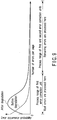
- FIG. 8 is a graph illustrating the relationship between the necessary correction capability and the elapsed time from data write in the semiconductor memory 2. As shown in FIG. 8 , as the elapsed time becomes long, the number of errors in the data written in the semiconductor memory 2 increases. The error correction capability is changed in accordance with the increase in the number of errors. The error correction capability of the first error correction unit 11 and that of the second error correction unit 13 are decided so that an excessive or insufficient error correction capability are used.
- the error correction capability of the first error correction unit 11 and that of the second error correction unit 13 are decided such that error correction can be done solely by the first error correction unit 11 when the elapsed time is short, while the first error correction unit 11 and the second error correction unit 13 can execute error correction when the elapsed time exceeds a predetermined time (the time when the number of errors abruptly increases).
- FIG. 9 shows the concept of the process range of the first error correction unit 11 and that of the second error correction unit 13 according to this embodiment.
- the abscissa in FIG. 9 represents the number of errors within a predetermined range (a page of a NAND flash memory) of the semiconductor memory 2.
- the ordinate represents the error occurrence probability.
- the broken line indicates the relationship before degradation of the semiconductor memory 2 (immediately after write).
- the solid line indicates the relationship after degradation of the semiconductor memory 2 (after the guaranteed data retention time has elapsed).
- the error correction capability of the first error correction unit 11 is decided such that only the first error correction unit 11 can correct all errors when the number of errors within the predetermined range is small. More specifically, the number of correctable bits, error correction method, and the number of bits of an error-correcting code are decided. For example, the error correction capability of the first error correction unit 11 is decided such that it can correct almost 100% of errors before degradation and about 99% of errors after degradation. On the other hand, the error correction capability of the second error correction unit 13 is decided to correct the remaining 1% of errors after degradation.
- the use probability of the second error correction unit 13 rises along with the increase in the error rate, as shown in FIG. 10 .
- the first error correction unit 11 which has a lower error correction capability but requires a shorter processing time and lower power consumption, corrects almost all errors.
- the second error correction unit 13 which requires a longer processing time and higher power consumption but has a higher error correction capability, corrects the remaining errors.
- the error correction circuit 1 can therefore achieve a short processing time, low power consumption, and small circuit scale while maintaining a high error correction capability.
- FIG. 11 shows the relationship between the error rate and the averaged Chien search range of the second error correction unit 13.
- the error correction capability of the first error correction unit 11 is set such that most errors can be corrected by only the first error correction unit 11, as described above. For this reason, even when the error rate is high, the second error correction unit 13 is rarely involved in error correction, as compared to the prior art (broken line).
- the plurality of first data blocks D1 to D8 each containing a corresponding one of a plurality of write data items are formed.
- the plurality of first error-correcting codes Dc1 to Dc8 are generated for the plurality of first data blocks D1 to D8, respectively.
- the second error-correcting code Dd is generated for a second data block formed from the plurality of first data blocks D1 to D8.
- error correction using the second error-correcting code Dd is executed for, of the first data blocks D1 to D8, only data containing errors even after error correction using the first error-correcting codes Dc1 to Dc8.
- This can greatly reduce the circuit scale of the second error correction unit 13 as compared to an example in which circuits for executing error correction using the second error-correcting code Dd are provided in correspondence with the plurality of first data blocks D1 to D8.
Landscapes
- Engineering & Computer Science (AREA)
- Theoretical Computer Science (AREA)
- Physics & Mathematics (AREA)
- General Engineering & Computer Science (AREA)
- General Physics & Mathematics (AREA)
- Quality & Reliability (AREA)
- Probability & Statistics with Applications (AREA)
- Computer Hardware Design (AREA)
- Computer Security & Cryptography (AREA)
- Techniques For Improving Reliability Of Storages (AREA)
- For Increasing The Reliability Of Semiconductor Memories (AREA)
- Detection And Correction Of Errors (AREA)
- Read Only Memory (AREA)
- Error Detection And Correction (AREA)
Claims (15)
- Halbleiterspeichervorrichtung (10), umfassend:eine Vielzahl von Erkennungscodegeneratoren (41), die konfiguriert sind, um eine Vielzahl von Erkennungscodes zu generieren, um jeweils Fehler in einer Vielzahl von Datenelementen zu erkennen;eine Vielzahl von ersten Korrekturcodegeneratoren (61), die konfiguriert sind, um eine Vielzahl von ersten Korrekturcodes zu generieren, um jeweils Fehler in einer Vielzahl von ersten Datenblöcken zu korrigieren, wobei jeder der ersten Datenblöcke eines der Datenelemente und einen entsprechenden Erkennungscode enthält;einen zweiten Korrekturcodegenerator (8), der konfiguriert ist, um einen zweiten Korrekturcode zum Korrigieren von Fehlern in einem zweiten Datenblock zu generieren, wobei der zweite Datenblock die Vielzahl von ersten Datenblöcken enthält; undeinen Halbleiterspeicher (2), der konfiguriert ist, den zweiten Datenblock, die Vielzahl von ersten Korrekturcodes und den zweiten Korrekturcode nichtflüchtig zu speichern,wobei der zweite Korrekturcodegenerator (8) eine Fehlerkorrekturfähigkeit aufweist, die höher ist als die der Vielzahl von ersten Korrekturcodegeneratoren (61).
- Vorrichtung (10) nach Anspruch 1, weiterhin Folgendes umfassend:einen ersten Korrektor (11), der konfiguriert ist, um die Fehler in den ersten Datenblöcken unter Verwendung der ersten Korrekturcodes zu korrigieren;einen Detektor (12), der konfiguriert ist, um unter Verwendung der Erkennungscodes Fehler in den durch den ersten Korrektor (11) korrigierten Datenelementen zu erkennen und eine erste Fehlerinformation zu generieren, die das Vorhandensein/Fehlen eines Fehlers in jedem der korrigierten Datenelemente darstellt; undeinen zweiten Korrektor (13), der konfiguriert ist, um die Fehler in den korrigierten Datenelementen, in einer Anzahl von Datenelementen, die die Fehler enthalten, unter Verwendung der ersten Fehlerinformation und des zweiten Korrekturcodes zu korrigieren.
- Vorrichtung (10) nach Anspruch 2, weiter umfassend einen Selektor (14), der zum Auswählen und Ausgeben von einem der ersten korrigierten Daten, die aus den durch den ersten Korrektor (11) korrigierten Datenelementen gebildet werden, und zweiten korrigierten Daten, die aus den durch den zweiten Korrektor (13) korrigierten Datenelementen gebildet werden, konfiguriert ist.
- Vorrichtung (10) nach Anspruch 3, wobei der Detektor (12) eine zweite Fehlerinformation generiert, die das Vorhandensein/Fehlen eines Fehlers in den ersten korrigierten Daten darstellt, und wobei der Selektor (14) die ersten korrigierten Daten ausgibt, wenn die ersten korrigierten Daten keinen Fehler enthalten, und die zweiten korrigierten Daten ausgibt, wenn die ersten korrigierten Daten einen Fehler auf der Basis der zweiten Fehlerinformation enthalten.
- Vorrichtung (10) nach Anspruch 1, wobei der Halbleiterspeicher (2) das Lesen oder Schreiben von Daten unter Verwendung einer ersten Größe als eine minimale Einheit ausführt und jedes der Datenelemente eine Größe gleich der ersten Größe aufweist.
- Vorrichtung (10) nach Anspruch 1, weiter eine temporäre Speicherschaltung umfassend, die konfiguriert ist, um die Datenelemente und die Erkennungscodes vorübergehend zu speichern.
- Vorrichtung (10) nach Anspruch 1, wobei die Erkennungscodegeneratoren (41) Prozesse zur parallelen Generierung der Erkennungscodes ausführen und die ersten Korrekturcodegeneratoren (61) Prozesse zur parallelen Generierung der ersten Korrekturcodes ausführen.
- Vorrichtung (10) nach Anspruch 2, wobei der zweite Korrektor (13) einen Korrekturprozess stoppt, wenn die durch den ersten Korrektor (11) korrigierten Datenelemente keinen Fehler enthalten.
- Vorrichtung (10) nach Anspruch 1, wobei der Halbleiterspeicher (2) ein NAND-Flash-Speicher ist.
- Verfahren zur Steuerung einer Halbleiterspeichervorrichtung (10), wobei das Verfahren Folgendes umfasst:Generieren (41) einer Vielzahl von Erkennungscodes, um jeweils Fehler in einer Vielzahl von Datenelementen zu erkennen;Generieren (61) einer Vielzahl erster Korrekturcodes, um jeweils Fehler in einer Vielzahl von ersten Datenblöcken zu korrigieren, wobei jeder der ersten Datenblöcke eines der Datenelemente und einen entsprechenden Erkennungscode enthält;Generieren (8) eines zweiten Korrekturcodes zum Korrigieren von Fehlern in einem zweiten Datenblock, wobei der zweite Datenblock die Vielzahl von ersten Datenblöcken enthält; undnichtflüchtiges Speichern (2) des zweiten Datenblocks, der Vielzahl erster Korrekturcodes und des zweiten Korrekturcodes,wobei der zweite Korrekturcode eine höhere Fehlerkorrekturfähigkeit als die der Vielzahl erster Korrekturcodes aufweist.
- Verfahren nach Anspruch 10, weiter Folgendes umfassend:Korrigieren (11) der Fehler in den ersten Datenblöcken unter Verwendung der ersten Korrekturcodes;Erkennen (12) von Fehlern in den Datenelementen unter Verwendung der Erkennungscodes, die unter Verwendung der ersten Korrekturcodes korrigiert wurden, wodurch eine erste Fehlerinformation generiert wird, die das Vorhandensein/Fehlen eines Fehlers in jedem der korrigierten Datenelemente darstellt; undKorrigieren (13) der Fehler der korrigierten Datenelemente in einer Anzahl von Datenelementen, die die Fehler enthalten, unter Verwendung der ersten Fehlerinformation und des zweiten Korrekturcodes.
- Verfahren nach Anspruch 11, weiter das Auswählen (14) und Ausgeben von einem von ersten korrigierten Daten umfassend, die aus den korrigierten Datenelementen unter Verwendung der ersten Korrekturcodes gebildet sind, und von zweiten korrigierten Daten, die aus den korrigierten Datenelementen unter Verwendung des zweiten Korrekturcodes gebildet sind.
- Verfahren nach Anspruch 12, weiter die Generieren einer zweiten Fehlerinformation umfassend, die das Vorhandensein/Fehlen eines Fehlers in den ersten korrigierten Daten darstellt, und
wobei in dem Ausgabeschritt auf der Basis der zweiten Fehlerinformation die ersten korrigierten Daten ausgegeben werden, wenn die ersten korrigierten Daten keinen Fehler enthalten, und die zweiten korrigierten Daten ausgegeben werden, wenn die ersten korrigierten Daten einen Fehler enthalten. - Verfahren nach Anspruch 10, wobei jedes der Datenelemente eine Größe aufweist, die gleich einer Größe von Lesedaten oder Schreibdaten ist.
- Verfahren nach Anspruch 10, wobei in dem Erkennungscode-Generierungsschritt Prozesse zur der Erkennungscodes parallel ausgeführt werden und in dem ersten Korrekturcode-Generierungsschritt Prozesse zur Generierungsschritt der ersten Korrekturcodes parallel ausgeführt werden.
Applications Claiming Priority (2)
| Application Number | Priority Date | Filing Date | Title |
|---|---|---|---|
| JP2007225996A JP4564520B2 (ja) | 2007-08-31 | 2007-08-31 | 半導体記憶装置およびその制御方法 |
| PCT/JP2008/063344 WO2009028281A1 (en) | 2007-08-31 | 2008-07-17 | Semiconductor memory device and method of controlling the same |
Publications (2)
| Publication Number | Publication Date |
|---|---|
| EP2186004A1 EP2186004A1 (de) | 2010-05-19 |
| EP2186004B1 true EP2186004B1 (de) | 2018-06-06 |
Family
ID=40011049
Family Applications (1)
| Application Number | Title | Priority Date | Filing Date |
|---|---|---|---|
| EP08791594.8A Not-in-force EP2186004B1 (de) | 2007-08-31 | 2008-07-17 | Halbleiterspeicherbauelement und verfahren zu seiner steuerung |
Country Status (7)
| Country | Link |
|---|---|
| US (14) | US8117517B2 (de) |
| EP (1) | EP2186004B1 (de) |
| JP (1) | JP4564520B2 (de) |
| KR (1) | KR101120346B1 (de) |
| CN (2) | CN102385538B (de) |
| TW (1) | TWI437571B (de) |
| WO (1) | WO2009028281A1 (de) |
Families Citing this family (187)
| Publication number | Priority date | Publication date | Assignee | Title |
|---|---|---|---|---|
| US20100041532A1 (en) * | 2007-01-08 | 2010-02-18 | Ashok Vishwanath Sathe | System of actuation of drive coupling to engage and disengage the drive to rotary tool holders |
| JP4564520B2 (ja) | 2007-08-31 | 2010-10-20 | 株式会社東芝 | 半導体記憶装置およびその制御方法 |
| JP4538034B2 (ja) * | 2007-09-26 | 2010-09-08 | 株式会社東芝 | 半導体記憶装置、及びその制御方法 |
| US7934052B2 (en) | 2007-12-27 | 2011-04-26 | Pliant Technology, Inc. | System and method for performing host initiated mass storage commands using a hierarchy of data structures |
| JP4461170B2 (ja) | 2007-12-28 | 2010-05-12 | 株式会社東芝 | メモリシステム |
| KR101077339B1 (ko) * | 2007-12-28 | 2011-10-26 | 가부시끼가이샤 도시바 | 반도체 기억 장치 |
| JP4489127B2 (ja) * | 2008-02-29 | 2010-06-23 | 株式会社東芝 | 半導体記憶装置 |
| JP4439569B2 (ja) * | 2008-04-24 | 2010-03-24 | 株式会社東芝 | メモリシステム |
| JP5056947B2 (ja) * | 2008-06-04 | 2012-10-24 | 富士通株式会社 | 情報処理装置、データ送信装置およびデータ送信装置のデータ転送方法 |
| JP4551958B2 (ja) * | 2008-12-22 | 2010-09-29 | 株式会社東芝 | 半導体記憶装置および半導体記憶装置の制御方法 |
| JP5317690B2 (ja) | 2008-12-27 | 2013-10-16 | 株式会社東芝 | メモリシステム |
| JP5221332B2 (ja) | 2008-12-27 | 2013-06-26 | 株式会社東芝 | メモリシステム |
| JP5268710B2 (ja) * | 2009-02-27 | 2013-08-21 | 株式会社東芝 | 半導体記憶装置 |
| JP2010204828A (ja) * | 2009-03-02 | 2010-09-16 | Renesas Electronics Corp | データ保護回路及び方法、並びにデータ処理装置 |
| JP5540969B2 (ja) * | 2009-09-11 | 2014-07-02 | ソニー株式会社 | 不揮発性メモリ装置、メモリコントローラ、およびメモリシステム |
| JP5680920B2 (ja) * | 2009-09-24 | 2015-03-04 | 株式会社テララコード研究所 | Rfidタグ、及びデータ管理システム |
| US9626243B2 (en) | 2009-12-11 | 2017-04-18 | Advanced Micro Devices, Inc. | Data error correction device and methods thereof |
| US8327225B2 (en) | 2010-01-04 | 2012-12-04 | Micron Technology, Inc. | Error correction in a stacked memory |
| JP5039160B2 (ja) * | 2010-03-02 | 2012-10-03 | 株式会社東芝 | 不揮発性半導体記憶システム |
| JP2011198272A (ja) * | 2010-03-23 | 2011-10-06 | Toshiba Corp | 半導体記憶装置および半導体記憶装置の制御方法 |
| JP5017407B2 (ja) | 2010-03-24 | 2012-09-05 | 株式会社東芝 | 半導体記憶装置 |
| JP4686645B2 (ja) * | 2010-07-29 | 2011-05-25 | 株式会社東芝 | 半導体記憶装置およびその制御方法 |
| JP5279785B2 (ja) | 2010-09-17 | 2013-09-04 | 株式会社東芝 | コントローラ、記憶装置、およびプログラム |
| JP5039193B2 (ja) | 2010-09-22 | 2012-10-03 | 株式会社東芝 | 半導体記憶装置および制御方法 |
| US8418026B2 (en) * | 2010-10-27 | 2013-04-09 | Sandisk Technologies Inc. | Hybrid error correction coding to address uncorrectable errors |
| JP2012137994A (ja) | 2010-12-27 | 2012-07-19 | Toshiba Corp | メモリシステムおよびその制御方法 |
| JP5269932B2 (ja) | 2011-03-01 | 2013-08-21 | 株式会社東芝 | コントローラ、データ記憶装置およびプログラム |
| KR101678919B1 (ko) | 2011-05-02 | 2016-11-24 | 삼성전자주식회사 | 메모리 시스템 및 에러 정정 방법 |
| KR101892251B1 (ko) * | 2011-05-09 | 2018-08-29 | 삼성전자주식회사 | 메모리 컨트롤러 및 메모리 컨트롤러의 동작 방법 |
| KR101800445B1 (ko) * | 2011-05-09 | 2017-12-21 | 삼성전자주식회사 | 메모리 컨트롤러 및 메모리 컨트롤러의 동작 방법 |
| JP5364807B2 (ja) * | 2011-06-08 | 2013-12-11 | パナソニック株式会社 | メモリコントローラ及び不揮発性記憶装置 |
| JP5426711B2 (ja) * | 2011-06-08 | 2014-02-26 | パナソニック株式会社 | メモリコントローラ及び不揮発性記憶装置 |
| JP5329689B2 (ja) * | 2011-06-08 | 2013-10-30 | パナソニック株式会社 | メモリコントローラ、不揮発性記憶装置 |
| US8910020B2 (en) | 2011-06-19 | 2014-12-09 | Sandisk Enterprise Ip Llc | Intelligent bit recovery for flash memory |
| US8909982B2 (en) | 2011-06-19 | 2014-12-09 | Sandisk Enterprise Ip Llc | System and method for detecting copyback programming problems |
| US8880977B2 (en) * | 2011-07-22 | 2014-11-04 | Sandisk Technologies Inc. | Systems and methods of storing data |
| JP2013029882A (ja) | 2011-07-26 | 2013-02-07 | Toshiba Corp | メモリコントローラ、半導体記憶装置および復号方法 |
| US8640013B2 (en) | 2011-09-22 | 2014-01-28 | Kabushiki Kaisha Toshiba | Storage device |
| US8793543B2 (en) | 2011-11-07 | 2014-07-29 | Sandisk Enterprise Ip Llc | Adaptive read comparison signal generation for memory systems |
| US8954822B2 (en) | 2011-11-18 | 2015-02-10 | Sandisk Enterprise Ip Llc | Data encoder and decoder using memory-specific parity-check matrix |
| US9048876B2 (en) | 2011-11-18 | 2015-06-02 | Sandisk Enterprise Ip Llc | Systems, methods and devices for multi-tiered error correction |
| US8924815B2 (en) | 2011-11-18 | 2014-12-30 | Sandisk Enterprise Ip Llc | Systems, methods and devices for decoding codewords having multiple parity segments |
| JP2013109567A (ja) | 2011-11-21 | 2013-06-06 | Toshiba Corp | ストレージデバイス及び誤り訂正方法 |
| US8645789B2 (en) * | 2011-12-22 | 2014-02-04 | Sandisk Technologies Inc. | Multi-phase ECC encoding using algebraic codes |
| CN102567134B (zh) * | 2012-01-06 | 2015-01-07 | 威盛电子股份有限公司 | 存储器模块的错误检查与校正系统以及方法 |
| WO2013105709A1 (ko) * | 2012-01-10 | 2013-07-18 | 조선대학교산학협력단 | 확장형 오류검출코드 기반의 오류 검출 장치 및 그 오류 검출 장치를 포함하는 자가검사 프로그래머블 연산 유닛 |
| KR101297318B1 (ko) * | 2012-02-17 | 2013-08-16 | 조선대학교산학협력단 | 대소 비교 연산 유닛을 위한 확장형 오류검출코드 기반의 오류 검출 장치 및 그 오류 검출 장치를 포함하는 자가검사 대소 비교 연산 유닛 |
| US8996950B2 (en) | 2012-02-23 | 2015-03-31 | Sandisk Technologies Inc. | Erasure correction using single error detection parity |
| JP5674700B2 (ja) | 2012-03-22 | 2015-02-25 | 株式会社東芝 | 符号化装置および符号化装置の制御方法、ならびに、記憶装置 |
| US9699263B1 (en) | 2012-08-17 | 2017-07-04 | Sandisk Technologies Llc. | Automatic read and write acceleration of data accessed by virtual machines |
| US9501398B2 (en) | 2012-12-26 | 2016-11-22 | Sandisk Technologies Llc | Persistent storage device with NVRAM for staging writes |
| US9043674B2 (en) * | 2012-12-26 | 2015-05-26 | Intel Corporation | Error detection and correction apparatus and method |
| US9239751B1 (en) | 2012-12-27 | 2016-01-19 | Sandisk Enterprise Ip Llc | Compressing data from multiple reads for error control management in memory systems |
| US9612948B2 (en) | 2012-12-27 | 2017-04-04 | Sandisk Technologies Llc | Reads and writes between a contiguous data block and noncontiguous sets of logical address blocks in a persistent storage device |
| US9454420B1 (en) | 2012-12-31 | 2016-09-27 | Sandisk Technologies Llc | Method and system of reading threshold voltage equalization |
| US9003264B1 (en) | 2012-12-31 | 2015-04-07 | Sandisk Enterprise Ip Llc | Systems, methods, and devices for multi-dimensional flash RAID data protection |
| JP5794240B2 (ja) * | 2013-02-05 | 2015-10-14 | ソニー株式会社 | 誤り検出訂正装置、誤り検出訂正方法、情報処理装置、および、プログラム |
| US9329928B2 (en) | 2013-02-20 | 2016-05-03 | Sandisk Enterprise IP LLC. | Bandwidth optimization in a non-volatile memory system |
| US9214965B2 (en) | 2013-02-20 | 2015-12-15 | Sandisk Enterprise Ip Llc | Method and system for improving data integrity in non-volatile storage |
| US9124300B2 (en) * | 2013-02-28 | 2015-09-01 | Sandisk Technologies Inc. | Error correction coding in non-volatile memory |
| US9870830B1 (en) | 2013-03-14 | 2018-01-16 | Sandisk Technologies Llc | Optimal multilevel sensing for reading data from a storage medium |
| US9244763B1 (en) | 2013-03-15 | 2016-01-26 | Sandisk Enterprise Ip Llc | System and method for updating a reading threshold voltage based on symbol transition information |
| US9136877B1 (en) | 2013-03-15 | 2015-09-15 | Sandisk Enterprise Ip Llc | Syndrome layered decoding for LDPC codes |
| US9236886B1 (en) | 2013-03-15 | 2016-01-12 | Sandisk Enterprise Ip Llc | Universal and reconfigurable QC-LDPC encoder |
| US9009576B1 (en) | 2013-03-15 | 2015-04-14 | Sandisk Enterprise Ip Llc | Adaptive LLR based on syndrome weight |
| US9092350B1 (en) | 2013-03-15 | 2015-07-28 | Sandisk Enterprise Ip Llc | Detection and handling of unbalanced errors in interleaved codewords |
| US9344117B2 (en) * | 2013-03-15 | 2016-05-17 | Mellanox Technologies, Ltd. | Methods and systems for error-correction decoding |
| US9367246B2 (en) | 2013-03-15 | 2016-06-14 | Sandisk Technologies Inc. | Performance optimization of data transfer for soft information generation |
| JP6174875B2 (ja) * | 2013-03-19 | 2017-08-02 | 日本放送協会 | 送信装置及び受信装置 |
| US10049037B2 (en) | 2013-04-05 | 2018-08-14 | Sandisk Enterprise Ip Llc | Data management in a storage system |
| US9170941B2 (en) | 2013-04-05 | 2015-10-27 | Sandisk Enterprises IP LLC | Data hardening in a storage system |
| US9159437B2 (en) | 2013-06-11 | 2015-10-13 | Sandisk Enterprise IP LLC. | Device and method for resolving an LM flag issue |
| US9524235B1 (en) | 2013-07-25 | 2016-12-20 | Sandisk Technologies Llc | Local hash value generation in non-volatile data storage systems |
| US9043517B1 (en) | 2013-07-25 | 2015-05-26 | Sandisk Enterprise Ip Llc | Multipass programming in buffers implemented in non-volatile data storage systems |
| US9384126B1 (en) | 2013-07-25 | 2016-07-05 | Sandisk Technologies Inc. | Methods and systems to avoid false negative results in bloom filters implemented in non-volatile data storage systems |
| US9235509B1 (en) | 2013-08-26 | 2016-01-12 | Sandisk Enterprise Ip Llc | Write amplification reduction by delaying read access to data written during garbage collection |
| US9639463B1 (en) | 2013-08-26 | 2017-05-02 | Sandisk Technologies Llc | Heuristic aware garbage collection scheme in storage systems |
| US9519577B2 (en) | 2013-09-03 | 2016-12-13 | Sandisk Technologies Llc | Method and system for migrating data between flash memory devices |
| US9442670B2 (en) | 2013-09-03 | 2016-09-13 | Sandisk Technologies Llc | Method and system for rebalancing data stored in flash memory devices |
| US9158349B2 (en) | 2013-10-04 | 2015-10-13 | Sandisk Enterprise Ip Llc | System and method for heat dissipation |
| US9323637B2 (en) | 2013-10-07 | 2016-04-26 | Sandisk Enterprise Ip Llc | Power sequencing and data hardening architecture |
| US9298608B2 (en) | 2013-10-18 | 2016-03-29 | Sandisk Enterprise Ip Llc | Biasing for wear leveling in storage systems |
| US9442662B2 (en) | 2013-10-18 | 2016-09-13 | Sandisk Technologies Llc | Device and method for managing die groups |
| US9436831B2 (en) | 2013-10-30 | 2016-09-06 | Sandisk Technologies Llc | Secure erase in a memory device |
| US9263156B2 (en) | 2013-11-07 | 2016-02-16 | Sandisk Enterprise Ip Llc | System and method for adjusting trip points within a storage device |
| US9244785B2 (en) | 2013-11-13 | 2016-01-26 | Sandisk Enterprise Ip Llc | Simulated power failure and data hardening |
| US9323609B2 (en) * | 2013-11-15 | 2016-04-26 | Intel Corporation | Data storage and variable length error correction information |
| US9152555B2 (en) | 2013-11-15 | 2015-10-06 | Sandisk Enterprise IP LLC. | Data management with modular erase in a data storage system |
| US9703816B2 (en) | 2013-11-19 | 2017-07-11 | Sandisk Technologies Llc | Method and system for forward reference logging in a persistent datastore |
| US9520197B2 (en) | 2013-11-22 | 2016-12-13 | Sandisk Technologies Llc | Adaptive erase of a storage device |
| US9280429B2 (en) | 2013-11-27 | 2016-03-08 | Sandisk Enterprise Ip Llc | Power fail latching based on monitoring multiple power supply voltages in a storage device |
| US9122636B2 (en) | 2013-11-27 | 2015-09-01 | Sandisk Enterprise Ip Llc | Hard power fail architecture |
| US9520162B2 (en) | 2013-11-27 | 2016-12-13 | Sandisk Technologies Llc | DIMM device controller supervisor |
| US9250676B2 (en) | 2013-11-29 | 2016-02-02 | Sandisk Enterprise Ip Llc | Power failure architecture and verification |
| US9582058B2 (en) | 2013-11-29 | 2017-02-28 | Sandisk Technologies Llc | Power inrush management of storage devices |
| US9092370B2 (en) | 2013-12-03 | 2015-07-28 | Sandisk Enterprise Ip Llc | Power failure tolerant cryptographic erase |
| US9235245B2 (en) | 2013-12-04 | 2016-01-12 | Sandisk Enterprise Ip Llc | Startup performance and power isolation |
| US9129665B2 (en) | 2013-12-17 | 2015-09-08 | Sandisk Enterprise Ip Llc | Dynamic brownout adjustment in a storage device |
| US9389956B2 (en) * | 2014-01-10 | 2016-07-12 | International Business Machines Corporation | Implementing ECC control for enhanced endurance and data retention of flash memories |
| US9549457B2 (en) | 2014-02-12 | 2017-01-17 | Sandisk Technologies Llc | System and method for redirecting airflow across an electronic assembly |
| US9497889B2 (en) | 2014-02-27 | 2016-11-15 | Sandisk Technologies Llc | Heat dissipation for substrate assemblies |
| US9703636B2 (en) | 2014-03-01 | 2017-07-11 | Sandisk Technologies Llc | Firmware reversion trigger and control |
| US9519319B2 (en) | 2014-03-14 | 2016-12-13 | Sandisk Technologies Llc | Self-supporting thermal tube structure for electronic assemblies |
| US9348377B2 (en) | 2014-03-14 | 2016-05-24 | Sandisk Enterprise Ip Llc | Thermal isolation techniques |
| US9485851B2 (en) | 2014-03-14 | 2016-11-01 | Sandisk Technologies Llc | Thermal tube assembly structures |
| US9448876B2 (en) | 2014-03-19 | 2016-09-20 | Sandisk Technologies Llc | Fault detection and prediction in storage devices |
| US9454448B2 (en) | 2014-03-19 | 2016-09-27 | Sandisk Technologies Llc | Fault testing in storage devices |
| US9390814B2 (en) | 2014-03-19 | 2016-07-12 | Sandisk Technologies Llc | Fault detection and prediction for data storage elements |
| US9626399B2 (en) | 2014-03-31 | 2017-04-18 | Sandisk Technologies Llc | Conditional updates for reducing frequency of data modification operations |
| US9626400B2 (en) | 2014-03-31 | 2017-04-18 | Sandisk Technologies Llc | Compaction of information in tiered data structure |
| US9390021B2 (en) | 2014-03-31 | 2016-07-12 | Sandisk Technologies Llc | Efficient cache utilization in a tiered data structure |
| US9697267B2 (en) | 2014-04-03 | 2017-07-04 | Sandisk Technologies Llc | Methods and systems for performing efficient snapshots in tiered data structures |
| US9703491B2 (en) | 2014-05-30 | 2017-07-11 | Sandisk Technologies Llc | Using history of unaligned writes to cache data and avoid read-modify-writes in a non-volatile storage device |
| US10372613B2 (en) | 2014-05-30 | 2019-08-06 | Sandisk Technologies Llc | Using sub-region I/O history to cache repeatedly accessed sub-regions in a non-volatile storage device |
| US10114557B2 (en) | 2014-05-30 | 2018-10-30 | Sandisk Technologies Llc | Identification of hot regions to enhance performance and endurance of a non-volatile storage device |
| US8891303B1 (en) | 2014-05-30 | 2014-11-18 | Sandisk Technologies Inc. | Method and system for dynamic word line based configuration of a three-dimensional memory device |
| US10656840B2 (en) | 2014-05-30 | 2020-05-19 | Sandisk Technologies Llc | Real-time I/O pattern recognition to enhance performance and endurance of a storage device |
| US10656842B2 (en) | 2014-05-30 | 2020-05-19 | Sandisk Technologies Llc | Using history of I/O sizes and I/O sequences to trigger coalesced writes in a non-volatile storage device |
| US10146448B2 (en) | 2014-05-30 | 2018-12-04 | Sandisk Technologies Llc | Using history of I/O sequences to trigger cached read ahead in a non-volatile storage device |
| US9070481B1 (en) | 2014-05-30 | 2015-06-30 | Sandisk Technologies Inc. | Internal current measurement for age measurements |
| US10162748B2 (en) | 2014-05-30 | 2018-12-25 | Sandisk Technologies Llc | Prioritizing garbage collection and block allocation based on I/O history for logical address regions |
| US9645749B2 (en) | 2014-05-30 | 2017-05-09 | Sandisk Technologies Llc | Method and system for recharacterizing the storage density of a memory device or a portion thereof |
| US9093160B1 (en) | 2014-05-30 | 2015-07-28 | Sandisk Technologies Inc. | Methods and systems for staggered memory operations |
| US9747048B2 (en) * | 2014-06-02 | 2017-08-29 | Micron Technology, Inc. | Systems and methods for packing data in a scalable memory system protocol |
| US9762262B2 (en) * | 2014-06-18 | 2017-09-12 | Alcatel Lucent | Hardware-efficient syndrome extraction for entangled quantum states |
| US9652381B2 (en) | 2014-06-19 | 2017-05-16 | Sandisk Technologies Llc | Sub-block garbage collection |
| JP2016031626A (ja) * | 2014-07-29 | 2016-03-07 | ソニー株式会社 | メモリコントローラ、記憶装置、情報処理システム、および、それらにおける制御方法。 |
| CN104269190B (zh) * | 2014-08-26 | 2017-10-17 | 上海华虹宏力半导体制造有限公司 | 存储器的数据校验方法 |
| US9703632B2 (en) * | 2014-11-07 | 2017-07-11 | Nxp B. V. | Sleep mode operation for volatile memory circuits |
| US9811417B2 (en) | 2015-03-12 | 2017-11-07 | Toshiba Memory Corporation | Semiconductor memory device |
| US9768808B2 (en) | 2015-04-08 | 2017-09-19 | Sandisk Technologies Llc | Method for modifying device-specific variable error correction settings |
| US9639282B2 (en) | 2015-05-20 | 2017-05-02 | Sandisk Technologies Llc | Variable bit encoding per NAND flash cell to improve device endurance and extend life of flash-based storage devices |
| US9606737B2 (en) | 2015-05-20 | 2017-03-28 | Sandisk Technologies Llc | Variable bit encoding per NAND flash cell to extend life of flash-based storage devices and preserve over-provisioning |
| JP6346123B2 (ja) | 2015-05-25 | 2018-06-20 | 東芝メモリ株式会社 | コントローラ、制御方法 |
| US9830084B2 (en) | 2015-12-03 | 2017-11-28 | Sandisk Technologies Llc | Writing logical groups of data to physical locations in memory using headers |
| US10013179B2 (en) | 2015-12-03 | 2018-07-03 | Sandisk Technologies Llc | Reading logical groups of data from physical locations in memory using headers |
| US10558525B2 (en) | 2016-06-30 | 2020-02-11 | Taiwan Semiconductor Manufacturing Company, Ltd. | Method of correcting errors in a memory array and a system for implementing the same |
| US9904595B1 (en) | 2016-08-23 | 2018-02-27 | Texas Instruments Incorporated | Error correction hardware with fault detection |
| KR102563162B1 (ko) * | 2016-09-05 | 2023-08-04 | 에스케이하이닉스 주식회사 | 집적회로 |
| US10403377B2 (en) * | 2017-06-26 | 2019-09-03 | Western Digital Technologies, Inc. | Non-volatile storage with adaptive redundancy |
| US10496548B2 (en) | 2018-02-07 | 2019-12-03 | Alibaba Group Holding Limited | Method and system for user-space storage I/O stack with user-space flash translation layer |
| CN108288489B (zh) * | 2018-04-24 | 2023-07-25 | 长鑫存储技术有限公司 | 半导体存储器循环冗余校验装置及半导体存储器 |
| WO2019222958A1 (en) | 2018-05-24 | 2019-11-28 | Alibaba Group Holding Limited | System and method for flash storage management using multiple open page stripes |
| US10921992B2 (en) | 2018-06-25 | 2021-02-16 | Alibaba Group Holding Limited | Method and system for data placement in a hard disk drive based on access frequency for improved IOPS and utilization efficiency |
| CN111902804B (zh) | 2018-06-25 | 2024-03-01 | 阿里巴巴集团控股有限公司 | 用于管理存储设备的资源并量化i/o请求成本的系统和方法 |
| US10996886B2 (en) | 2018-08-02 | 2021-05-04 | Alibaba Group Holding Limited | Method and system for facilitating atomicity and latency assurance on variable sized I/O |
| US11327929B2 (en) | 2018-09-17 | 2022-05-10 | Alibaba Group Holding Limited | Method and system for reduced data movement compression using in-storage computing and a customized file system |
| TWI714277B (zh) * | 2018-09-28 | 2020-12-21 | 台灣積體電路製造股份有限公司 | 記憶體錯誤偵測及校正 |
| US11204826B2 (en) | 2018-09-28 | 2021-12-21 | Taiwan Semiconductor Manufacturing Company, Ltd. | Memory error detection and correction |
| US11216333B2 (en) * | 2018-10-16 | 2022-01-04 | Micron Technology, Inc. | Methods and devices for error correction |
| US10977122B2 (en) | 2018-12-31 | 2021-04-13 | Alibaba Group Holding Limited | System and method for facilitating differentiated error correction in high-density flash devices |
| US11061735B2 (en) | 2019-01-02 | 2021-07-13 | Alibaba Group Holding Limited | System and method for offloading computation to storage nodes in distributed system |
| US11132291B2 (en) | 2019-01-04 | 2021-09-28 | Alibaba Group Holding Limited | System and method of FPGA-executed flash translation layer in multiple solid state drives |
| US11200337B2 (en) | 2019-02-11 | 2021-12-14 | Alibaba Group Holding Limited | System and method for user data isolation |
| US11005501B2 (en) | 2019-02-19 | 2021-05-11 | Micron Technology, Inc. | Error correction on a memory device |
| US11169873B2 (en) * | 2019-05-21 | 2021-11-09 | Alibaba Group Holding Limited | Method and system for extending lifespan and enhancing throughput in a high-density solid state drive |
| US10860223B1 (en) | 2019-07-18 | 2020-12-08 | Alibaba Group Holding Limited | Method and system for enhancing a distributed storage system by decoupling computation and network tasks |
| US11617282B2 (en) | 2019-10-01 | 2023-03-28 | Alibaba Group Holding Limited | System and method for reshaping power budget of cabinet to facilitate improved deployment density of servers |
| US11126561B2 (en) | 2019-10-01 | 2021-09-21 | Alibaba Group Holding Limited | Method and system for organizing NAND blocks and placing data to facilitate high-throughput for random writes in a solid state drive |
| US11449455B2 (en) | 2020-01-15 | 2022-09-20 | Alibaba Group Holding Limited | Method and system for facilitating a high-capacity object storage system with configuration agility and mixed deployment flexibility |
| US11379447B2 (en) | 2020-02-06 | 2022-07-05 | Alibaba Group Holding Limited | Method and system for enhancing IOPS of a hard disk drive system based on storing metadata in host volatile memory and data in non-volatile memory using a shared controller |
| US11200114B2 (en) | 2020-03-17 | 2021-12-14 | Alibaba Group Holding Limited | System and method for facilitating elastic error correction code in memory |
| US11449386B2 (en) | 2020-03-20 | 2022-09-20 | Alibaba Group Holding Limited | Method and system for optimizing persistent memory on data retention, endurance, and performance for host memory |
| US11301173B2 (en) | 2020-04-20 | 2022-04-12 | Alibaba Group Holding Limited | Method and system for facilitating evaluation of data access frequency and allocation of storage device resources |
| US11385833B2 (en) | 2020-04-20 | 2022-07-12 | Alibaba Group Holding Limited | Method and system for facilitating a light-weight garbage collection with a reduced utilization of resources |
| US11281575B2 (en) | 2020-05-11 | 2022-03-22 | Alibaba Group Holding Limited | Method and system for facilitating data placement and control of physical addresses with multi-queue I/O blocks |
| US11494115B2 (en) | 2020-05-13 | 2022-11-08 | Alibaba Group Holding Limited | System method for facilitating memory media as file storage device based on real-time hashing by performing integrity check with a cyclical redundancy check (CRC) |
| US11461262B2 (en) | 2020-05-13 | 2022-10-04 | Alibaba Group Holding Limited | Method and system for facilitating a converged computation and storage node in a distributed storage system |
| US11218165B2 (en) | 2020-05-15 | 2022-01-04 | Alibaba Group Holding Limited | Memory-mapped two-dimensional error correction code for multi-bit error tolerance in DRAM |
| US11507499B2 (en) | 2020-05-19 | 2022-11-22 | Alibaba Group Holding Limited | System and method for facilitating mitigation of read/write amplification in data compression |
| US11556277B2 (en) | 2020-05-19 | 2023-01-17 | Alibaba Group Holding Limited | System and method for facilitating improved performance in ordering key-value storage with input/output stack simplification |
| US11263132B2 (en) | 2020-06-11 | 2022-03-01 | Alibaba Group Holding Limited | Method and system for facilitating log-structure data organization |
| US11422931B2 (en) | 2020-06-17 | 2022-08-23 | Alibaba Group Holding Limited | Method and system for facilitating a physically isolated storage unit for multi-tenancy virtualization |
| US11354200B2 (en) | 2020-06-17 | 2022-06-07 | Alibaba Group Holding Limited | Method and system for facilitating data recovery and version rollback in a storage device |
| KR20210157863A (ko) * | 2020-06-22 | 2021-12-29 | 에스케이하이닉스 주식회사 | 메모리, 메모리 시스템 및 메모리의 동작 방법 |
| JP2022012874A (ja) * | 2020-07-02 | 2022-01-17 | キオクシア株式会社 | 受信端末、通信システム、およびプログラム |
| US11354233B2 (en) | 2020-07-27 | 2022-06-07 | Alibaba Group Holding Limited | Method and system for facilitating fast crash recovery in a storage device |
| US11372774B2 (en) | 2020-08-24 | 2022-06-28 | Alibaba Group Holding Limited | Method and system for a solid state drive with on-chip memory integration |
| CN114203228B (zh) * | 2020-09-18 | 2023-09-15 | 长鑫存储技术有限公司 | 存储器 |
| EP4227944B1 (de) | 2020-09-18 | 2025-07-02 | Changxin Memory Technologies, Inc. | Speicher |
| US11487465B2 (en) | 2020-12-11 | 2022-11-01 | Alibaba Group Holding Limited | Method and system for a local storage engine collaborating with a solid state drive controller |
| US11734115B2 (en) | 2020-12-28 | 2023-08-22 | Alibaba Group Holding Limited | Method and system for facilitating write latency reduction in a queue depth of one scenario |
| US11416365B2 (en) | 2020-12-30 | 2022-08-16 | Alibaba Group Holding Limited | Method and system for open NAND block detection and correction in an open-channel SSD |
| US11726699B2 (en) | 2021-03-30 | 2023-08-15 | Alibaba Singapore Holding Private Limited | Method and system for facilitating multi-stream sequential read performance improvement with reduced read amplification |
| US11461173B1 (en) | 2021-04-21 | 2022-10-04 | Alibaba Singapore Holding Private Limited | Method and system for facilitating efficient data compression based on error correction code and reorganization of data placement |
| US11476874B1 (en) | 2021-05-14 | 2022-10-18 | Alibaba Singapore Holding Private Limited | Method and system for facilitating a storage server with hybrid memory for journaling and data storage |
| JPWO2022239623A1 (de) * | 2021-05-14 | 2022-11-17 |
Family Cites Families (96)
| Publication number | Priority date | Publication date | Assignee | Title |
|---|---|---|---|---|
| US3993445A (en) * | 1974-11-27 | 1976-11-23 | Allegheny Ludlum Industries, Inc. | Sintered ferritic stainless steel |
| US3980444A (en) * | 1975-01-22 | 1976-09-14 | Allegheny Ludlum Industries, Inc. | Sintered liquid phase stainless steel |
| US4014680A (en) * | 1975-01-22 | 1977-03-29 | Allegheny Ludlum Industries, Inc. | Prealloyed stainless steel powder for liquid phase sintering |
| US4420336A (en) * | 1982-02-11 | 1983-12-13 | Scm Corporation | Process of improving corrosion resistance in porous stainless steel bodies and article |
| US4535034A (en) * | 1983-12-30 | 1985-08-13 | Nippon Steel Corporation | High Al heat-resistant alloy steels having Al coating thereon |
| US4562039A (en) * | 1984-06-27 | 1985-12-31 | Pall Corporation | Porous metal article and method of making |
| JPS6151253A (ja) * | 1984-08-20 | 1986-03-13 | Nec Corp | 誤り訂正回路 |
| EP0213725A3 (de) * | 1985-08-05 | 1987-07-29 | BREHK Ventures | Verfahren und Vorrichtung zur Abscheidung und Einäscherung von Partikeln aus dem Abgas von Dieselmotoren |
| JP2696212B2 (ja) | 1987-05-06 | 1998-01-14 | セイコーエプソン株式会社 | 誤り訂正装置 |
| DE3818281A1 (de) * | 1988-03-10 | 1989-09-21 | Schwaebische Huettenwerke Gmbh | Abgasfilter |
| SE461032B (sv) * | 1988-03-21 | 1989-12-18 | Roby Teknik Ab | Anordning vid en foerpackningsmaskin foer att ombesoerja en steril fyllningsatmosfaer |
| US5019311A (en) * | 1989-02-23 | 1991-05-28 | Koslow Technologies Corporation | Process for the production of materials characterized by a continuous web matrix or force point bonding |
| DE4021495A1 (de) * | 1990-07-05 | 1992-01-09 | Schwaebische Huettenwerke Gmbh | Abgasfilter |
| DE4029749A1 (de) * | 1990-09-20 | 1992-03-26 | Schwaebische Huettenwerke Gmbh | Filter |
| DE4110285A1 (de) * | 1991-03-28 | 1992-10-01 | Schwaebische Huettenwerke Gmbh | Filter- oder katalysatorkoerper |
| US5204067A (en) * | 1991-07-11 | 1993-04-20 | Schwaebische Huettenwerke Gmbh | Filter |
| JP2721099B2 (ja) * | 1991-12-18 | 1998-03-04 | インターナショナル・ビジネス・マシーンズ・コーポレイション | エラーバースト修正のための試行錯誤方法及びマルチバイトエラーの修正方法 |
| DE4234930A1 (de) * | 1992-10-16 | 1994-04-21 | Schwaebische Huettenwerke Gmbh | Filter zum Abscheiden von Verunreinigungen aus Abgasen |
| JPH07138713A (ja) * | 1993-11-15 | 1995-05-30 | Daido Steel Co Ltd | Fe基合金粉末及び高耐食性焼結体の製造方法 |
| JP3366721B2 (ja) | 1994-03-11 | 2003-01-14 | 富士通株式会社 | 多数バイトのエラー訂正装置 |
| JPH1097471A (ja) * | 1996-09-20 | 1998-04-14 | Toshiba Corp | メモリデータのエラー訂正方法、及びエラー訂正方式 |
| JPH10207726A (ja) * | 1997-01-23 | 1998-08-07 | Oki Electric Ind Co Ltd | 半導体ディスク装置 |
| DE19741498B4 (de) * | 1997-09-20 | 2008-07-03 | Evonik Degussa Gmbh | Herstellung eines Keramik-Edelstahlgewebe-Verbundes |
| JP3865946B2 (ja) | 1998-08-06 | 2007-01-10 | 富士通株式会社 | 文字メッセージ通信システム、文字メッセージ通信装置、文字メッセージ通信サーバ、文字メッセージ通信プログラムを記録したコンピュータ読み取り可能な記録媒体、文字メッセージ通信管理プログラムを記録したコンピュータ読み取り可能な記録媒体、文字メッセージ送受信方法及び文字メッセージ通信管理方法 |
| KR100287018B1 (ko) * | 1998-08-07 | 2001-04-16 | 윤종용 | 에러 정정 회로를 구비한 반도체 메모리 장치 |
| JP2000101447A (ja) | 1998-09-24 | 2000-04-07 | Sanyo Electric Co Ltd | 誤り訂正装置および誤り訂正方法 |
| JP2000181807A (ja) * | 1998-12-16 | 2000-06-30 | Murata Mach Ltd | 記録媒体のデータ検査方法及び装置 |
| JP2000269824A (ja) * | 1999-01-12 | 2000-09-29 | Matsushita Electric Ind Co Ltd | データ符号化装置及びデータ復号化装置 |
| JP3871471B2 (ja) * | 1999-07-12 | 2007-01-24 | 松下電器産業株式会社 | Ecc回路搭載半導体記憶装置及びその検査方法 |
| JP3975245B2 (ja) * | 1999-12-16 | 2007-09-12 | 株式会社ルネサステクノロジ | 記録再生装置および半導体メモリ |
| JP2001297038A (ja) * | 2000-04-11 | 2001-10-26 | Toshiba Corp | データ記憶装置および記録媒体並びに記録媒体制御方法 |
| US6322605B1 (en) * | 2000-05-31 | 2001-11-27 | Corning Incorporated | Diesel exhaust filters |
| US6328779B1 (en) * | 2000-05-31 | 2001-12-11 | Corning Incorporated | Microwave regenerated diesel particular filter and method of making the same |
| WO2001098872A2 (en) | 2000-06-22 | 2001-12-27 | Microchip Technology Incorporated | A method of checking eeprom data with an embedded crc |
| US6941505B2 (en) * | 2000-09-12 | 2005-09-06 | Hitachi, Ltd. | Data processing system and data processing method |
| US7020811B2 (en) * | 2001-04-24 | 2006-03-28 | Sun Microsystems, Inc. | System and method for verifying error detection/correction logic |
| US20020174397A1 (en) * | 2001-05-16 | 2002-11-21 | Fujitsu Limited | Method for error detection/correction of multilevel cell memory and multilevel cell memory having error detection/correction function |
| SE0102102D0 (sv) * | 2001-06-13 | 2001-06-13 | Hoeganaes Ab | High density stainless steel products and method for the preparation thereof |
| JP4437519B2 (ja) * | 2001-08-23 | 2010-03-24 | スパンション エルエルシー | 多値セルメモリ用のメモリコントローラ |
| JP3981268B2 (ja) * | 2001-12-28 | 2007-09-26 | 日本電産サンキョー株式会社 | 不揮発性メモリ及びそのデータ更新方法 |
| EP1469093B1 (de) * | 2002-01-24 | 2011-04-20 | Sumitomo (SEI) Steel Wire Corp. | Verfahren zur herstellung einer hitzebeständigen stahlfeder |
| CN1288658C (zh) * | 2002-04-25 | 2006-12-06 | 三洋电机株式会社 | 数据处理装置 |
| US20040015771A1 (en) * | 2002-07-16 | 2004-01-22 | Menahem Lasser | Error correction for non-volatile memory |
| EP1460542B1 (de) * | 2003-03-19 | 2018-10-31 | Micron Technology, INC. | Integriertes Speichersystem mit mindestens einem nichtflüchtigen Speicher und einem automatischen Fehlerkorrektor |
| JP2005051739A (ja) * | 2003-07-16 | 2005-02-24 | Ricoh Co Ltd | 画像処理装置、画像処理方法および該画像処理方法による画像処理プログラムならびに該画像処理プログラムを収容した記録媒体 |
| US7389465B2 (en) * | 2004-01-30 | 2008-06-17 | Micron Technology, Inc. | Error detection and correction scheme for a memory device |
| JP2005216437A (ja) * | 2004-01-30 | 2005-08-11 | Matsushita Electric Ind Co Ltd | 誤り訂正機能付き半導体記憶装置およびその誤り訂正方法 |
| JP2005267719A (ja) * | 2004-03-17 | 2005-09-29 | Sanyo Electric Co Ltd | 符号化装置 |
| KR100539261B1 (ko) * | 2004-05-04 | 2005-12-27 | 삼성전자주식회사 | 디지털 데이터의 부호화 장치와 dvd로의 기록 장치 및그 방법 |
| US7322002B2 (en) * | 2004-05-26 | 2008-01-22 | Micron Technology, Inc. | Erasure pointer error correction |
| US7334179B2 (en) * | 2004-06-04 | 2008-02-19 | Broadcom Corporation | Method and system for detecting and correcting errors while accessing memory devices in microprocessor systems |
| EP1797645B1 (de) * | 2004-08-30 | 2018-08-01 | Google LLC | Systeme und verfahren zur bereitstellung von verwaltung nichtflüchtiger speicher in drahtlosen telefonen |
| US7409623B2 (en) * | 2004-11-04 | 2008-08-05 | Sigmatel, Inc. | System and method of reading non-volatile computer memory |
| US7849381B2 (en) * | 2004-12-21 | 2010-12-07 | Sandisk Corporation | Method for copying data in reprogrammable non-volatile memory |
| KR100680473B1 (ko) * | 2005-04-11 | 2007-02-08 | 주식회사 하이닉스반도체 | 액세스 시간이 감소된 플래시 메모리 장치 |
| US20060256615A1 (en) * | 2005-05-10 | 2006-11-16 | Larson Thane M | Horizontal and vertical error correction coding (ECC) system and method |
| JP4734033B2 (ja) * | 2005-05-30 | 2011-07-27 | 株式会社東芝 | 記憶装置 |
| EP1741685B1 (de) * | 2005-07-05 | 2014-04-30 | MANN+HUMMEL Innenraumfilter GmbH & Co. KG | Poröser beta-SiC-haltiger keramischer Formkörper und Verfahren zu dessen Herstellung. |
| GB2428496A (en) * | 2005-07-15 | 2007-01-31 | Global Silicon Ltd | Error correction for flash memory |
| EP1934745A2 (de) * | 2005-09-27 | 2008-06-25 | Nxp B.V. | Fehlerdetektions-/korrekturschaltung und entsprechendes verfahren |
| US7512864B2 (en) * | 2005-09-30 | 2009-03-31 | Josef Zeevi | System and method of accessing non-volatile computer memory |
| KR100737912B1 (ko) * | 2005-10-11 | 2007-07-10 | 삼성전자주식회사 | 반도체 메모리 장치의 에러 검출 및 정정 회로 |
| KR100681429B1 (ko) * | 2005-10-24 | 2007-02-15 | 삼성전자주식회사 | 반도체 메모리 장치 및 그것의 비트 에러 검출 방법 |
| JP4660353B2 (ja) * | 2005-11-01 | 2011-03-30 | 株式会社東芝 | 記憶媒体再生装置 |
| JP4575288B2 (ja) * | 2005-12-05 | 2010-11-04 | 株式会社東芝 | 記憶媒体、記憶媒体再生装置、記憶媒体再生方法および記憶媒体再生プログラム |
| US7562283B2 (en) * | 2005-12-27 | 2009-07-14 | D.S.P. Group Ltd. | Systems and methods for error correction using binary coded hexidecimal or hamming decoding |
| US7562285B2 (en) * | 2006-01-11 | 2009-07-14 | Rambus Inc. | Unidirectional error code transfer for a bidirectional data link |
| JP2007242162A (ja) * | 2006-03-09 | 2007-09-20 | Toshiba Corp | 半導体記憶装置 |
| JP4662278B2 (ja) * | 2006-04-28 | 2011-03-30 | 富士通株式会社 | エラー訂正装置、符号器、復号器、方法及び情報記憶装置 |
| US7707481B2 (en) * | 2006-05-16 | 2010-04-27 | Pitney Bowes Inc. | System and method for efficient uncorrectable error detection in flash memory |
| US20070268905A1 (en) * | 2006-05-18 | 2007-11-22 | Sigmatel, Inc. | Non-volatile memory error correction system and method |
| US7774684B2 (en) * | 2006-06-30 | 2010-08-10 | Intel Corporation | Reliability, availability, and serviceability in a memory device |
| JP4896605B2 (ja) * | 2006-07-04 | 2012-03-14 | 株式会社東芝 | 不揮発性半導体記憶システム |
| JP5052070B2 (ja) * | 2006-08-23 | 2012-10-17 | ルネサスエレクトロニクス株式会社 | データ読み出し回路及びデータ読み出し方法 |
| US7739576B2 (en) * | 2006-08-31 | 2010-06-15 | Micron Technology, Inc. | Variable strength ECC |
| US8171380B2 (en) * | 2006-10-10 | 2012-05-01 | Marvell World Trade Ltd. | Adaptive systems and methods for storing and retrieving data to and from memory cells |
| TW200828328A (en) * | 2006-12-28 | 2008-07-01 | Genesys Logic Inc | Method of improving accessing reliability of flash memory |
| KR100845529B1 (ko) * | 2007-01-03 | 2008-07-10 | 삼성전자주식회사 | 플래시 메모리 장치의 이씨씨 제어기 및 그것을 포함한메모리 시스템 |
| KR100842680B1 (ko) * | 2007-01-08 | 2008-07-01 | 삼성전자주식회사 | 플래시 메모리 장치의 오류 정정 컨트롤러 및 그것을포함하는 메모리 시스템 |
| US8051358B2 (en) * | 2007-07-06 | 2011-11-01 | Micron Technology, Inc. | Error recovery storage along a nand-flash string |
| JP4564520B2 (ja) * | 2007-08-31 | 2010-10-20 | 株式会社東芝 | 半導体記憶装置およびその制御方法 |
| US8095851B2 (en) * | 2007-09-06 | 2012-01-10 | Siliconsystems, Inc. | Storage subsystem capable of adjusting ECC settings based on monitored conditions |
| JP4538034B2 (ja) * | 2007-09-26 | 2010-09-08 | 株式会社東芝 | 半導体記憶装置、及びその制御方法 |
| JP5166074B2 (ja) * | 2008-02-29 | 2013-03-21 | 株式会社東芝 | 半導体記憶装置、その制御方法、および誤り訂正システム |
| US8276043B2 (en) * | 2008-03-01 | 2012-09-25 | Kabushiki Kaisha Toshiba | Memory system |
| JP4672743B2 (ja) | 2008-03-01 | 2011-04-20 | 株式会社東芝 | 誤り訂正装置および誤り訂正方法 |
| JP2010015195A (ja) * | 2008-06-30 | 2010-01-21 | Toshiba Corp | 記憶制御装置及び記憶制御方法 |
| JP2010015197A (ja) * | 2008-06-30 | 2010-01-21 | Toshiba Corp | ストレージ制御装置、データ復元装置およびストレージシステム |
| JP2010009548A (ja) | 2008-06-30 | 2010-01-14 | Toshiba Corp | 記憶装置、制御装置、記憶システム、および記憶方法 |
| JP5242264B2 (ja) * | 2008-07-07 | 2013-07-24 | 株式会社東芝 | データ制御装置、ストレージシステムおよびプログラム |
| US8296620B2 (en) * | 2008-08-26 | 2012-10-23 | Seagate Technology Llc | Data devices including multiple error correction codes and methods of utilizing |
| JP4551958B2 (ja) * | 2008-12-22 | 2010-09-29 | 株式会社東芝 | 半導体記憶装置および半導体記憶装置の制御方法 |
| JP5268710B2 (ja) | 2009-02-27 | 2013-08-21 | 株式会社東芝 | 半導体記憶装置 |
| US7941696B2 (en) * | 2009-08-11 | 2011-05-10 | Texas Memory Systems, Inc. | Flash-based memory system with static or variable length page stripes including data protection information and auxiliary protection stripes |
| JP4660632B2 (ja) | 2010-07-29 | 2011-03-30 | 株式会社東芝 | 半導体記憶装置 |
| JP2012137994A (ja) | 2010-12-27 | 2012-07-19 | Toshiba Corp | メモリシステムおよびその制御方法 |
-
2007
- 2007-08-31 JP JP2007225996A patent/JP4564520B2/ja not_active Expired - Fee Related
-
2008
- 2008-07-17 KR KR1020097018201A patent/KR101120346B1/ko not_active Expired - Fee Related
- 2008-07-17 CN CN201110252163.5A patent/CN102385538B/zh not_active Expired - Fee Related
- 2008-07-17 CN CN2008800066548A patent/CN101622603B/zh not_active Expired - Fee Related
- 2008-07-17 WO PCT/JP2008/063344 patent/WO2009028281A1/en not_active Ceased
- 2008-07-17 EP EP08791594.8A patent/EP2186004B1/de not_active Not-in-force
- 2008-07-24 TW TW097128194A patent/TWI437571B/zh not_active IP Right Cessation
-
2009
- 2009-03-16 US US12/404,861 patent/US8117517B2/en active Active
-
2011
- 2011-04-20 US US13/090,539 patent/US8196008B2/en not_active Expired - Fee Related
- 2011-04-20 US US13/090,499 patent/US8069394B2/en active Active
-
2012
- 2012-05-07 US US13/465,624 patent/US8386881B2/en not_active Expired - Fee Related
-
2013
- 2013-02-04 US US13/757,935 patent/US8732544B2/en active Active
-
2014
- 2014-03-31 US US14/231,140 patent/US8959411B2/en active Active
-
2015
- 2015-01-21 US US14/601,664 patent/US9384090B2/en active Active
- 2015-10-22 US US14/920,510 patent/US20160041875A1/en not_active Abandoned
-
2017
- 2017-02-01 US US15/421,746 patent/US20170141799A1/en not_active Abandoned
-
2019
- 2019-03-19 US US16/357,696 patent/US11038536B2/en active Active
-
2021
- 2021-05-11 US US17/317,280 patent/US11575395B2/en active Active
-
2022
- 2022-12-29 US US18/148,060 patent/US12074616B2/en active Active
-
2024
- 2024-07-12 US US18/771,866 patent/US12413251B2/en active Active
-
2025
- 2025-08-07 US US19/293,282 patent/US20250365021A1/en active Pending
Non-Patent Citations (1)
| Title |
|---|
| None * |
Also Published As
Similar Documents
| Publication | Publication Date | Title |
|---|---|---|
| US12413251B2 (en) | Semiconductor memory device and method of controlling the same | |
| JP4538034B2 (ja) | 半導体記憶装置、及びその制御方法 | |
| JP4660632B2 (ja) | 半導体記憶装置 | |
| JP4686645B2 (ja) | 半導体記憶装置およびその制御方法 |
Legal Events
| Date | Code | Title | Description |
|---|---|---|---|
| PUAI | Public reference made under article 153(3) epc to a published international application that has entered the european phase |
Free format text: ORIGINAL CODE: 0009012 |
|
| 17P | Request for examination filed |
Effective date: 20090824 |
|
| AK | Designated contracting states |
Kind code of ref document: A1 Designated state(s): AT BE BG CH CY CZ DE DK EE ES FI FR GB GR HR HU IE IS IT LI LT LU LV MC MT NL NO PL PT RO SE SI SK TR |
|
| AX | Request for extension of the european patent |
Extension state: AL BA MK RS |
|
| DAX | Request for extension of the european patent (deleted) | ||
| 17Q | First examination report despatched |
Effective date: 20160311 |
|
| RAP1 | Party data changed (applicant data changed or rights of an application transferred) |
Owner name: TOSHIBA MEMORY CORPORATION |
|
| GRAP | Despatch of communication of intention to grant a patent |
Free format text: ORIGINAL CODE: EPIDOSNIGR1 |
|
| STAA | Information on the status of an ep patent application or granted ep patent |
Free format text: STATUS: GRANT OF PATENT IS INTENDED |
|
| INTG | Intention to grant announced |
Effective date: 20180228 |
|
| GRAS | Grant fee paid |
Free format text: ORIGINAL CODE: EPIDOSNIGR3 |
|
| GRAA | (expected) grant |
Free format text: ORIGINAL CODE: 0009210 |
|
| STAA | Information on the status of an ep patent application or granted ep patent |
Free format text: STATUS: THE PATENT HAS BEEN GRANTED |
|
| AK | Designated contracting states |
Kind code of ref document: B1 Designated state(s): AT BE BG CH CY CZ DE DK EE ES FI FR GB GR HR HU IE IS IT LI LT LU LV MC MT NL NO PL PT RO SE SI SK TR |
|
| REG | Reference to a national code |
Ref country code: GB Ref legal event code: FG4D |
|
| REG | Reference to a national code |
Ref country code: CH Ref legal event code: EP Ref country code: AT Ref legal event code: REF Ref document number: 1006836 Country of ref document: AT Kind code of ref document: T Effective date: 20180615 |
|
| REG | Reference to a national code |
Ref country code: IE Ref legal event code: FG4D |
|
| REG | Reference to a national code |
Ref country code: FR Ref legal event code: PLFP Year of fee payment: 11 |
|
| REG | Reference to a national code |
Ref country code: DE Ref legal event code: R096 Ref document number: 602008055543 Country of ref document: DE |
|
| REG | Reference to a national code |
Ref country code: NL Ref legal event code: MP Effective date: 20180606 |
|
| REG | Reference to a national code |
Ref country code: LT Ref legal event code: MG4D |
|
| PG25 | Lapsed in a contracting state [announced via postgrant information from national office to epo] |
Ref country code: FI Free format text: LAPSE BECAUSE OF FAILURE TO SUBMIT A TRANSLATION OF THE DESCRIPTION OR TO PAY THE FEE WITHIN THE PRESCRIBED TIME-LIMIT Effective date: 20180606 Ref country code: LT Free format text: LAPSE BECAUSE OF FAILURE TO SUBMIT A TRANSLATION OF THE DESCRIPTION OR TO PAY THE FEE WITHIN THE PRESCRIBED TIME-LIMIT Effective date: 20180606 Ref country code: BG Free format text: LAPSE BECAUSE OF FAILURE TO SUBMIT A TRANSLATION OF THE DESCRIPTION OR TO PAY THE FEE WITHIN THE PRESCRIBED TIME-LIMIT Effective date: 20180906 Ref country code: CY Free format text: LAPSE BECAUSE OF FAILURE TO SUBMIT A TRANSLATION OF THE DESCRIPTION OR TO PAY THE FEE WITHIN THE PRESCRIBED TIME-LIMIT Effective date: 20180606 Ref country code: ES Free format text: LAPSE BECAUSE OF FAILURE TO SUBMIT A TRANSLATION OF THE DESCRIPTION OR TO PAY THE FEE WITHIN THE PRESCRIBED TIME-LIMIT Effective date: 20180606 Ref country code: NO Free format text: LAPSE BECAUSE OF FAILURE TO SUBMIT A TRANSLATION OF THE DESCRIPTION OR TO PAY THE FEE WITHIN THE PRESCRIBED TIME-LIMIT Effective date: 20180906 Ref country code: SE Free format text: LAPSE BECAUSE OF FAILURE TO SUBMIT A TRANSLATION OF THE DESCRIPTION OR TO PAY THE FEE WITHIN THE PRESCRIBED TIME-LIMIT Effective date: 20180606 |
|
| PG25 | Lapsed in a contracting state [announced via postgrant information from national office to epo] |
Ref country code: LV Free format text: LAPSE BECAUSE OF FAILURE TO SUBMIT A TRANSLATION OF THE DESCRIPTION OR TO PAY THE FEE WITHIN THE PRESCRIBED TIME-LIMIT Effective date: 20180606 Ref country code: GR Free format text: LAPSE BECAUSE OF FAILURE TO SUBMIT A TRANSLATION OF THE DESCRIPTION OR TO PAY THE FEE WITHIN THE PRESCRIBED TIME-LIMIT Effective date: 20180907 Ref country code: HR Free format text: LAPSE BECAUSE OF FAILURE TO SUBMIT A TRANSLATION OF THE DESCRIPTION OR TO PAY THE FEE WITHIN THE PRESCRIBED TIME-LIMIT Effective date: 20180606 |
|
| REG | Reference to a national code |
Ref country code: AT Ref legal event code: MK05 Ref document number: 1006836 Country of ref document: AT Kind code of ref document: T Effective date: 20180606 |
|
| PG25 | Lapsed in a contracting state [announced via postgrant information from national office to epo] |
Ref country code: NL Free format text: LAPSE BECAUSE OF FAILURE TO SUBMIT A TRANSLATION OF THE DESCRIPTION OR TO PAY THE FEE WITHIN THE PRESCRIBED TIME-LIMIT Effective date: 20180606 |
|
| PG25 | Lapsed in a contracting state [announced via postgrant information from national office to epo] |
Ref country code: AT Free format text: LAPSE BECAUSE OF FAILURE TO SUBMIT A TRANSLATION OF THE DESCRIPTION OR TO PAY THE FEE WITHIN THE PRESCRIBED TIME-LIMIT Effective date: 20180606 Ref country code: PL Free format text: LAPSE BECAUSE OF FAILURE TO SUBMIT A TRANSLATION OF THE DESCRIPTION OR TO PAY THE FEE WITHIN THE PRESCRIBED TIME-LIMIT Effective date: 20180606 Ref country code: CZ Free format text: LAPSE BECAUSE OF FAILURE TO SUBMIT A TRANSLATION OF THE DESCRIPTION OR TO PAY THE FEE WITHIN THE PRESCRIBED TIME-LIMIT Effective date: 20180606 Ref country code: SK Free format text: LAPSE BECAUSE OF FAILURE TO SUBMIT A TRANSLATION OF THE DESCRIPTION OR TO PAY THE FEE WITHIN THE PRESCRIBED TIME-LIMIT Effective date: 20180606 Ref country code: RO Free format text: LAPSE BECAUSE OF FAILURE TO SUBMIT A TRANSLATION OF THE DESCRIPTION OR TO PAY THE FEE WITHIN THE PRESCRIBED TIME-LIMIT Effective date: 20180606 Ref country code: IS Free format text: LAPSE BECAUSE OF FAILURE TO SUBMIT A TRANSLATION OF THE DESCRIPTION OR TO PAY THE FEE WITHIN THE PRESCRIBED TIME-LIMIT Effective date: 20181006 Ref country code: EE Free format text: LAPSE BECAUSE OF FAILURE TO SUBMIT A TRANSLATION OF THE DESCRIPTION OR TO PAY THE FEE WITHIN THE PRESCRIBED TIME-LIMIT Effective date: 20180606 |
|
| PG25 | Lapsed in a contracting state [announced via postgrant information from national office to epo] |
Ref country code: IT Free format text: LAPSE BECAUSE OF FAILURE TO SUBMIT A TRANSLATION OF THE DESCRIPTION OR TO PAY THE FEE WITHIN THE PRESCRIBED TIME-LIMIT Effective date: 20180606 |
|
| REG | Reference to a national code |
Ref country code: CH Ref legal event code: PL |
|
| REG | Reference to a national code |
Ref country code: DE Ref legal event code: R097 Ref document number: 602008055543 Country of ref document: DE |
|
| PG25 | Lapsed in a contracting state [announced via postgrant information from national office to epo] |
Ref country code: MC Free format text: LAPSE BECAUSE OF FAILURE TO SUBMIT A TRANSLATION OF THE DESCRIPTION OR TO PAY THE FEE WITHIN THE PRESCRIBED TIME-LIMIT Effective date: 20180606 Ref country code: LU Free format text: LAPSE BECAUSE OF NON-PAYMENT OF DUE FEES Effective date: 20180717 |
|
| REG | Reference to a national code |
Ref country code: BE Ref legal event code: MM Effective date: 20180731 |
|
| PLBE | No opposition filed within time limit |
Free format text: ORIGINAL CODE: 0009261 |
|
| STAA | Information on the status of an ep patent application or granted ep patent |
Free format text: STATUS: NO OPPOSITION FILED WITHIN TIME LIMIT |
|
| REG | Reference to a national code |
Ref country code: IE Ref legal event code: MM4A |
|
| PG25 | Lapsed in a contracting state [announced via postgrant information from national office to epo] |
Ref country code: LI Free format text: LAPSE BECAUSE OF NON-PAYMENT OF DUE FEES Effective date: 20180731 Ref country code: CH Free format text: LAPSE BECAUSE OF NON-PAYMENT OF DUE FEES Effective date: 20180731 Ref country code: IE Free format text: LAPSE BECAUSE OF NON-PAYMENT OF DUE FEES Effective date: 20180717 |
|
| 26N | No opposition filed |
Effective date: 20190307 |
|
| PG25 | Lapsed in a contracting state [announced via postgrant information from national office to epo] |
Ref country code: SI Free format text: LAPSE BECAUSE OF FAILURE TO SUBMIT A TRANSLATION OF THE DESCRIPTION OR TO PAY THE FEE WITHIN THE PRESCRIBED TIME-LIMIT Effective date: 20180606 Ref country code: BE Free format text: LAPSE BECAUSE OF NON-PAYMENT OF DUE FEES Effective date: 20180731 Ref country code: DK Free format text: LAPSE BECAUSE OF FAILURE TO SUBMIT A TRANSLATION OF THE DESCRIPTION OR TO PAY THE FEE WITHIN THE PRESCRIBED TIME-LIMIT Effective date: 20180606 |
|
| PG25 | Lapsed in a contracting state [announced via postgrant information from national office to epo] |
Ref country code: MT Free format text: LAPSE BECAUSE OF NON-PAYMENT OF DUE FEES Effective date: 20180717 |
|
| PG25 | Lapsed in a contracting state [announced via postgrant information from national office to epo] |
Ref country code: TR Free format text: LAPSE BECAUSE OF FAILURE TO SUBMIT A TRANSLATION OF THE DESCRIPTION OR TO PAY THE FEE WITHIN THE PRESCRIBED TIME-LIMIT Effective date: 20180606 |
|
| PG25 | Lapsed in a contracting state [announced via postgrant information from national office to epo] |
Ref country code: HU Free format text: LAPSE BECAUSE OF FAILURE TO SUBMIT A TRANSLATION OF THE DESCRIPTION OR TO PAY THE FEE WITHIN THE PRESCRIBED TIME-LIMIT; INVALID AB INITIO Effective date: 20080717 Ref country code: PT Free format text: LAPSE BECAUSE OF FAILURE TO SUBMIT A TRANSLATION OF THE DESCRIPTION OR TO PAY THE FEE WITHIN THE PRESCRIBED TIME-LIMIT Effective date: 20180606 |
|
| PGFP | Annual fee paid to national office [announced via postgrant information from national office to epo] |
Ref country code: FR Payment date: 20200611 Year of fee payment: 13 |
|
| PGFP | Annual fee paid to national office [announced via postgrant information from national office to epo] |
Ref country code: GB Payment date: 20200708 Year of fee payment: 13 Ref country code: DE Payment date: 20200707 Year of fee payment: 13 |
|
| REG | Reference to a national code |
Ref country code: DE Ref legal event code: R119 Ref document number: 602008055543 Country of ref document: DE |
|
| GBPC | Gb: european patent ceased through non-payment of renewal fee |
Effective date: 20210717 |
|
| PG25 | Lapsed in a contracting state [announced via postgrant information from national office to epo] |
Ref country code: GB Free format text: LAPSE BECAUSE OF NON-PAYMENT OF DUE FEES Effective date: 20210717 Ref country code: DE Free format text: LAPSE BECAUSE OF NON-PAYMENT OF DUE FEES Effective date: 20220201 |
|
| PG25 | Lapsed in a contracting state [announced via postgrant information from national office to epo] |
Ref country code: FR Free format text: LAPSE BECAUSE OF NON-PAYMENT OF DUE FEES Effective date: 20210731 |