EP2115092B1 - Leuchtstoffe bestehend aus dotierten granaten für pcleds - Google Patents
Leuchtstoffe bestehend aus dotierten granaten für pcleds Download PDFInfo
- Publication number
- EP2115092B1 EP2115092B1 EP08707688A EP08707688A EP2115092B1 EP 2115092 B1 EP2115092 B1 EP 2115092B1 EP 08707688 A EP08707688 A EP 08707688A EP 08707688 A EP08707688 A EP 08707688A EP 2115092 B1 EP2115092 B1 EP 2115092B1
- Authority
- EP
- European Patent Office
- Prior art keywords
- phosphor
- light source
- lighting unit
- zno
- primary light
- Prior art date
- Legal status (The legal status is an assumption and is not a legal conclusion. Google has not performed a legal analysis and makes no representation as to the accuracy of the status listed.)
- Not-in-force
Links
- 238000000034 method Methods 0.000 claims abstract description 41
- 238000006243 chemical reaction Methods 0.000 claims abstract description 35
- 230000008569 process Effects 0.000 claims abstract description 17
- 238000002360 preparation method Methods 0.000 claims abstract description 13
- 239000002223 garnet Substances 0.000 claims abstract description 11
- OAICVXFJPJFONN-UHFFFAOYSA-N Phosphorus Chemical compound [P] OAICVXFJPJFONN-UHFFFAOYSA-N 0.000 claims description 127
- 239000000463 material Substances 0.000 claims description 34
- 239000000203 mixture Substances 0.000 claims description 28
- 238000000576 coating method Methods 0.000 claims description 22
- 239000000126 substance Substances 0.000 claims description 20
- 239000011248 coating agent Substances 0.000 claims description 19
- 230000005855 radiation Effects 0.000 claims description 19
- 229910052684 Cerium Inorganic materials 0.000 claims description 17
- 239000002245 particle Substances 0.000 claims description 14
- 229910052776 Thorium Inorganic materials 0.000 claims description 12
- 229910052797 bismuth Inorganic materials 0.000 claims description 11
- 238000002156 mixing Methods 0.000 claims description 10
- 239000002243 precursor Substances 0.000 claims description 10
- -1 cerium-activated phosphor Chemical class 0.000 claims description 9
- XLOMVQKBTHCTTD-UHFFFAOYSA-N zinc oxide Inorganic materials [Zn]=O XLOMVQKBTHCTTD-UHFFFAOYSA-N 0.000 claims description 9
- 229910052782 aluminium Inorganic materials 0.000 claims description 8
- 229910052787 antimony Inorganic materials 0.000 claims description 8
- PNEYBMLMFCGWSK-UHFFFAOYSA-N aluminium oxide Inorganic materials [O-2].[O-2].[O-2].[Al+3].[Al+3] PNEYBMLMFCGWSK-UHFFFAOYSA-N 0.000 claims description 7
- 230000003287 optical effect Effects 0.000 claims description 6
- 229910052761 rare earth metal Inorganic materials 0.000 claims description 6
- 239000002019 doping agent Substances 0.000 claims description 5
- 238000001035 drying Methods 0.000 claims description 5
- 229910052751 metal Inorganic materials 0.000 claims description 5
- 239000002184 metal Substances 0.000 claims description 5
- XAGFODPZIPBFFR-UHFFFAOYSA-N aluminium Chemical compound [Al] XAGFODPZIPBFFR-UHFFFAOYSA-N 0.000 claims description 4
- 150000001875 compounds Chemical class 0.000 claims description 4
- 239000002105 nanoparticle Substances 0.000 claims description 4
- 229920000647 polyepoxide Polymers 0.000 claims description 4
- 238000001556 precipitation Methods 0.000 claims description 4
- 229920002050 silicone resin Polymers 0.000 claims description 4
- 239000000725 suspension Substances 0.000 claims description 4
- ZSLUVFAKFWKJRC-IGMARMGPSA-N 232Th Chemical compound [232Th] ZSLUVFAKFWKJRC-IGMARMGPSA-N 0.000 claims description 3
- 239000004593 Epoxy Substances 0.000 claims description 3
- WATWJIUSRGPENY-UHFFFAOYSA-N antimony atom Chemical compound [Sb] WATWJIUSRGPENY-UHFFFAOYSA-N 0.000 claims description 3
- 125000000524 functional group Chemical group 0.000 claims description 3
- 238000001694 spray drying Methods 0.000 claims description 3
- 239000007858 starting material Substances 0.000 claims description 3
- 229910002601 GaN Inorganic materials 0.000 claims description 2
- JMASRVWKEDWRBT-UHFFFAOYSA-N Gallium nitride Chemical compound [Ga]#N JMASRVWKEDWRBT-UHFFFAOYSA-N 0.000 claims description 2
- JCXGWMGPZLAOME-UHFFFAOYSA-N bismuth atom Chemical compound [Bi] JCXGWMGPZLAOME-UHFFFAOYSA-N 0.000 claims description 2
- 230000008878 coupling Effects 0.000 claims description 2
- 238000010168 coupling process Methods 0.000 claims description 2
- 238000005859 coupling reaction Methods 0.000 claims description 2
- 238000005401 electroluminescence Methods 0.000 claims description 2
- 229910052738 indium Inorganic materials 0.000 claims description 2
- APFVFJFRJDLVQX-UHFFFAOYSA-N indium atom Chemical compound [In] APFVFJFRJDLVQX-UHFFFAOYSA-N 0.000 claims description 2
- 238000005424 photoluminescence Methods 0.000 claims description 2
- SBIBMFFZSBJNJF-UHFFFAOYSA-N selenium;zinc Chemical compound [Se]=[Zn] SBIBMFFZSBJNJF-UHFFFAOYSA-N 0.000 claims description 2
- 238000003980 solgel method Methods 0.000 claims description 2
- VYPSYNLAJGMNEJ-UHFFFAOYSA-N Silicium dioxide Chemical compound O=[Si]=O VYPSYNLAJGMNEJ-UHFFFAOYSA-N 0.000 claims 12
- GWEVSGVZZGPLCZ-UHFFFAOYSA-N Titan oxide Chemical compound O=[Ti]=O GWEVSGVZZGPLCZ-UHFFFAOYSA-N 0.000 claims 12
- MCMNRKCIXSYSNV-UHFFFAOYSA-N Zirconium dioxide Chemical compound O=[Zr]=O MCMNRKCIXSYSNV-UHFFFAOYSA-N 0.000 claims 12
- 229910052681 coesite Inorganic materials 0.000 claims 6
- 229910052593 corundum Inorganic materials 0.000 claims 6
- 229910052906 cristobalite Inorganic materials 0.000 claims 6
- 239000000377 silicon dioxide Substances 0.000 claims 6
- 229910052682 stishovite Inorganic materials 0.000 claims 6
- 229910052905 tridymite Inorganic materials 0.000 claims 6
- 229910001845 yogo sapphire Inorganic materials 0.000 claims 6
- LENJPRSQISBMDN-UHFFFAOYSA-N [Y].[Ce] Chemical compound [Y].[Ce] LENJPRSQISBMDN-UHFFFAOYSA-N 0.000 claims 1
- AZDRQVAHHNSJOQ-UHFFFAOYSA-N alumane Chemical compound [AlH3] AZDRQVAHHNSJOQ-UHFFFAOYSA-N 0.000 claims 1
- 239000004411 aluminium Substances 0.000 claims 1
- 239000010410 layer Substances 0.000 description 23
- 239000000243 solution Substances 0.000 description 20
- 229910019655 synthetic inorganic crystalline material Inorganic materials 0.000 description 12
- XLYOFNOQVPJJNP-UHFFFAOYSA-N water Substances O XLYOFNOQVPJJNP-UHFFFAOYSA-N 0.000 description 12
- 229910052727 yttrium Inorganic materials 0.000 description 11
- QGZKDVFQNNGYKY-UHFFFAOYSA-N Ammonia Chemical compound N QGZKDVFQNNGYKY-UHFFFAOYSA-N 0.000 description 10
- 238000013461 design Methods 0.000 description 10
- 238000009792 diffusion process Methods 0.000 description 10
- 230000008901 benefit Effects 0.000 description 9
- 239000011230 binding agent Substances 0.000 description 9
- 239000000919 ceramic Substances 0.000 description 8
- GWXLDORMOJMVQZ-UHFFFAOYSA-N cerium Chemical compound [Ce] GWXLDORMOJMVQZ-UHFFFAOYSA-N 0.000 description 8
- 239000002244 precipitate Substances 0.000 description 8
- 239000004065 semiconductor Substances 0.000 description 8
- 229910018072 Al 2 O 3 Inorganic materials 0.000 description 7
- 239000012298 atmosphere Substances 0.000 description 7
- 229910019990 cerium-doped yttrium aluminum garnet Inorganic materials 0.000 description 7
- 239000008367 deionised water Substances 0.000 description 7
- 229910021641 deionized water Inorganic materials 0.000 description 7
- LYCAIKOWRPUZTN-UHFFFAOYSA-N Ethylene glycol Chemical compound OCCO LYCAIKOWRPUZTN-UHFFFAOYSA-N 0.000 description 6
- 241000219739 Lens Species 0.000 description 6
- XSQUKJJJFZCRTK-UHFFFAOYSA-N Urea Chemical compound NC(N)=O XSQUKJJJFZCRTK-UHFFFAOYSA-N 0.000 description 6
- KRKNYBCHXYNGOX-UHFFFAOYSA-N citric acid Chemical compound OC(=O)CC(O)(C(O)=O)CC(O)=O KRKNYBCHXYNGOX-UHFFFAOYSA-N 0.000 description 6
- 238000004519 manufacturing process Methods 0.000 description 6
- BVKZGUZCCUSVTD-UHFFFAOYSA-M Bicarbonate Chemical class OC([O-])=O BVKZGUZCCUSVTD-UHFFFAOYSA-M 0.000 description 5
- 240000004322 Lens culinaris Species 0.000 description 5
- 229910002651 NO3 Inorganic materials 0.000 description 5
- NHNBFGGVMKEFGY-UHFFFAOYSA-N Nitrate Chemical compound [O-][N+]([O-])=O NHNBFGGVMKEFGY-UHFFFAOYSA-N 0.000 description 5
- 229910004298 SiO 2 Inorganic materials 0.000 description 5
- 229910010413 TiO 2 Inorganic materials 0.000 description 5
- 239000012190 activator Substances 0.000 description 5
- 229910021529 ammonia Inorganic materials 0.000 description 5
- 238000009826 distribution Methods 0.000 description 5
- 238000000295 emission spectrum Methods 0.000 description 5
- 239000001257 hydrogen Substances 0.000 description 5
- 229910052739 hydrogen Inorganic materials 0.000 description 5
- 238000005286 illumination Methods 0.000 description 5
- 150000002500 ions Chemical class 0.000 description 5
- 229920003227 poly(N-vinyl carbazole) Polymers 0.000 description 5
- 239000000758 substrate Substances 0.000 description 5
- ATRRKUHOCOJYRX-UHFFFAOYSA-N Ammonium bicarbonate Chemical compound [NH4+].OC([O-])=O ATRRKUHOCOJYRX-UHFFFAOYSA-N 0.000 description 4
- 229910000013 Ammonium bicarbonate Inorganic materials 0.000 description 4
- UFHFLCQGNIYNRP-UHFFFAOYSA-N Hydrogen Chemical compound [H][H] UFHFLCQGNIYNRP-UHFFFAOYSA-N 0.000 description 4
- 230000032683 aging Effects 0.000 description 4
- JGDITNMASUZKPW-UHFFFAOYSA-K aluminium trichloride hexahydrate Chemical compound O.O.O.O.O.O.Cl[Al](Cl)Cl JGDITNMASUZKPW-UHFFFAOYSA-K 0.000 description 4
- 229940009861 aluminum chloride hexahydrate Drugs 0.000 description 4
- 235000012538 ammonium bicarbonate Nutrition 0.000 description 4
- 239000001099 ammonium carbonate Substances 0.000 description 4
- 239000012300 argon atmosphere Substances 0.000 description 4
- SQKWGPOIVHMUNF-UHFFFAOYSA-K cerium(3+);trichloride;hexahydrate Chemical compound O.O.O.O.O.O.[Cl-].[Cl-].[Cl-].[Ce+3] SQKWGPOIVHMUNF-UHFFFAOYSA-K 0.000 description 4
- 239000010408 film Substances 0.000 description 4
- 239000007789 gas Substances 0.000 description 4
- 238000003825 pressing Methods 0.000 description 4
- 239000000047 product Substances 0.000 description 4
- 150000002910 rare earth metals Chemical class 0.000 description 4
- 229920005989 resin Polymers 0.000 description 4
- 239000011347 resin Substances 0.000 description 4
- 150000003384 small molecules Chemical class 0.000 description 4
- 239000007787 solid Substances 0.000 description 4
- 239000002904 solvent Substances 0.000 description 4
- 238000005118 spray pyrolysis Methods 0.000 description 4
- IINACGXCEZNYTF-UHFFFAOYSA-K trichloroyttrium;hexahydrate Chemical compound O.O.O.O.O.O.[Cl-].[Cl-].[Cl-].[Y+3] IINACGXCEZNYTF-UHFFFAOYSA-K 0.000 description 4
- UGFAIRIUMAVXCW-UHFFFAOYSA-N Carbon monoxide Chemical compound [O+]#[C-] UGFAIRIUMAVXCW-UHFFFAOYSA-N 0.000 description 3
- 229910052693 Europium Inorganic materials 0.000 description 3
- GEIAQOFPUVMAGM-UHFFFAOYSA-N ZrO Inorganic materials [Zr]=O GEIAQOFPUVMAGM-UHFFFAOYSA-N 0.000 description 3
- 230000015572 biosynthetic process Effects 0.000 description 3
- 229910002091 carbon monoxide Inorganic materials 0.000 description 3
- 239000000470 constituent Substances 0.000 description 3
- ZYGHJZDHTFUPRJ-UHFFFAOYSA-N coumarin Chemical compound C1=CC=C2OC(=O)C=CC2=C1 ZYGHJZDHTFUPRJ-UHFFFAOYSA-N 0.000 description 3
- 239000013078 crystal Substances 0.000 description 3
- 238000005090 crystal field Methods 0.000 description 3
- 239000006185 dispersion Substances 0.000 description 3
- 230000000694 effects Effects 0.000 description 3
- 238000005516 engineering process Methods 0.000 description 3
- 238000005530 etching Methods 0.000 description 3
- 230000005284 excitation Effects 0.000 description 3
- 238000011049 filling Methods 0.000 description 3
- 238000010304 firing Methods 0.000 description 3
- 229910052733 gallium Inorganic materials 0.000 description 3
- 239000011521 glass Substances 0.000 description 3
- 239000004570 mortar (masonry) Substances 0.000 description 3
- 150000004767 nitrides Chemical class 0.000 description 3
- 229920000642 polymer Polymers 0.000 description 3
- 229920001296 polysiloxane Polymers 0.000 description 3
- 230000009467 reduction Effects 0.000 description 3
- 239000012266 salt solution Substances 0.000 description 3
- 238000005507 spraying Methods 0.000 description 3
- CSCPPACGZOOCGX-UHFFFAOYSA-N Acetone Chemical compound CC(C)=O CSCPPACGZOOCGX-UHFFFAOYSA-N 0.000 description 2
- 229910019142 PO4 Inorganic materials 0.000 description 2
- 229910052777 Praseodymium Inorganic materials 0.000 description 2
- BQCADISMDOOEFD-UHFFFAOYSA-N Silver Chemical compound [Ag] BQCADISMDOOEFD-UHFFFAOYSA-N 0.000 description 2
- 239000005083 Zinc sulfide Substances 0.000 description 2
- 230000009102 absorption Effects 0.000 description 2
- 239000012491 analyte Substances 0.000 description 2
- 238000001354 calcination Methods 0.000 description 2
- 239000004202 carbamide Substances 0.000 description 2
- 150000001768 cations Chemical class 0.000 description 2
- CETPSERCERDGAM-UHFFFAOYSA-N ceric oxide Chemical compound O=[Ce]=O CETPSERCERDGAM-UHFFFAOYSA-N 0.000 description 2
- HSJPMRKMPBAUAU-UHFFFAOYSA-N cerium(3+);trinitrate Chemical compound [Ce+3].[O-][N+]([O-])=O.[O-][N+]([O-])=O.[O-][N+]([O-])=O HSJPMRKMPBAUAU-UHFFFAOYSA-N 0.000 description 2
- 229910000422 cerium(IV) oxide Inorganic materials 0.000 description 2
- 229910052804 chromium Inorganic materials 0.000 description 2
- 238000000975 co-precipitation Methods 0.000 description 2
- 238000007796 conventional method Methods 0.000 description 2
- 238000010586 diagram Methods 0.000 description 2
- 238000001704 evaporation Methods 0.000 description 2
- 230000008020 evaporation Effects 0.000 description 2
- 239000000835 fiber Substances 0.000 description 2
- RHZWSUVWRRXEJF-UHFFFAOYSA-N indium tin Chemical compound [In].[Sn] RHZWSUVWRRXEJF-UHFFFAOYSA-N 0.000 description 2
- 238000000462 isostatic pressing Methods 0.000 description 2
- 229910052748 manganese Inorganic materials 0.000 description 2
- 239000010445 mica Substances 0.000 description 2
- 229910052618 mica group Inorganic materials 0.000 description 2
- MEFBJEMVZONFCJ-UHFFFAOYSA-N molybdate Chemical compound [O-][Mo]([O-])(=O)=O MEFBJEMVZONFCJ-UHFFFAOYSA-N 0.000 description 2
- SIWVEOZUMHYXCS-UHFFFAOYSA-N oxo(oxoyttriooxy)yttrium Chemical compound O=[Y]O[Y]=O SIWVEOZUMHYXCS-UHFFFAOYSA-N 0.000 description 2
- 235000021317 phosphate Nutrition 0.000 description 2
- 150000003013 phosphoric acid derivatives Chemical class 0.000 description 2
- BASFCYQUMIYNBI-UHFFFAOYSA-N platinum Chemical compound [Pt] BASFCYQUMIYNBI-UHFFFAOYSA-N 0.000 description 2
- 229920002098 polyfluorene Polymers 0.000 description 2
- 239000000843 powder Substances 0.000 description 2
- 238000006862 quantum yield reaction Methods 0.000 description 2
- 230000009103 reabsorption Effects 0.000 description 2
- 238000005215 recombination Methods 0.000 description 2
- 230000006798 recombination Effects 0.000 description 2
- 238000011160 research Methods 0.000 description 2
- 238000012552 review Methods 0.000 description 2
- 238000000926 separation method Methods 0.000 description 2
- 229910052709 silver Inorganic materials 0.000 description 2
- 239000004332 silver Substances 0.000 description 2
- SQGYOTSLMSWVJD-UHFFFAOYSA-N silver(1+) nitrate Chemical compound [Ag+].[O-]N(=O)=O SQGYOTSLMSWVJD-UHFFFAOYSA-N 0.000 description 2
- 230000003595 spectral effect Effects 0.000 description 2
- 229910001887 tin oxide Inorganic materials 0.000 description 2
- LSGOVYNHVSXFFJ-UHFFFAOYSA-N vanadate(3-) Chemical compound [O-][V]([O-])([O-])=O LSGOVYNHVSXFFJ-UHFFFAOYSA-N 0.000 description 2
- 229910019901 yttrium aluminum garnet Inorganic materials 0.000 description 2
- VWQVUPCCIRVNHF-UHFFFAOYSA-N yttrium atom Chemical compound [Y] VWQVUPCCIRVNHF-UHFFFAOYSA-N 0.000 description 2
- 229910052984 zinc sulfide Inorganic materials 0.000 description 2
- DRDVZXDWVBGGMH-UHFFFAOYSA-N zinc;sulfide Chemical compound [S-2].[Zn+2] DRDVZXDWVBGGMH-UHFFFAOYSA-N 0.000 description 2
- BNGXYYYYKUGPPF-UHFFFAOYSA-M (3-methylphenyl)methyl-triphenylphosphanium;chloride Chemical compound [Cl-].CC1=CC=CC(C[P+](C=2C=CC=CC=2)(C=2C=CC=CC=2)C=2C=CC=CC=2)=C1 BNGXYYYYKUGPPF-UHFFFAOYSA-M 0.000 description 1
- NGDQQLAVJWUYSF-UHFFFAOYSA-N 4-methyl-2-phenyl-1,3-thiazole-5-sulfonyl chloride Chemical compound S1C(S(Cl)(=O)=O)=C(C)N=C1C1=CC=CC=C1 NGDQQLAVJWUYSF-UHFFFAOYSA-N 0.000 description 1
- 206010001497 Agitation Diseases 0.000 description 1
- VEXZGXHMUGYJMC-UHFFFAOYSA-M Chloride anion Chemical compound [Cl-] VEXZGXHMUGYJMC-UHFFFAOYSA-M 0.000 description 1
- WQZGKKKJIJFFOK-GASJEMHNSA-N Glucose Natural products OC[C@H]1OC(O)[C@H](O)[C@@H](O)[C@@H]1O WQZGKKKJIJFFOK-GASJEMHNSA-N 0.000 description 1
- 206010021143 Hypoxia Diseases 0.000 description 1
- 229910052765 Lutetium Inorganic materials 0.000 description 1
- BPQQTUXANYXVAA-UHFFFAOYSA-N Orthosilicate Chemical compound [O-][Si]([O-])([O-])[O-] BPQQTUXANYXVAA-UHFFFAOYSA-N 0.000 description 1
- 229910004283 SiO 4 Inorganic materials 0.000 description 1
- 229910052771 Terbium Inorganic materials 0.000 description 1
- 238000000124 X-ray reflection spectroscopy Methods 0.000 description 1
- 238000010521 absorption reaction Methods 0.000 description 1
- 238000000862 absorption spectrum Methods 0.000 description 1
- 150000001242 acetic acid derivatives Chemical class 0.000 description 1
- 230000006978 adaptation Effects 0.000 description 1
- 238000001856 aerosol method Methods 0.000 description 1
- AUCDRFABNLOFRE-UHFFFAOYSA-N alumane;indium Chemical compound [AlH3].[In] AUCDRFABNLOFRE-UHFFFAOYSA-N 0.000 description 1
- JNDMLEXHDPKVFC-UHFFFAOYSA-N aluminum;oxygen(2-);yttrium(3+) Chemical compound [O-2].[O-2].[O-2].[Al+3].[Y+3] JNDMLEXHDPKVFC-UHFFFAOYSA-N 0.000 description 1
- 150000001450 anions Chemical class 0.000 description 1
- 238000000137 annealing Methods 0.000 description 1
- FAPDDOBMIUGHIN-UHFFFAOYSA-K antimony trichloride Chemical compound Cl[Sb](Cl)Cl FAPDDOBMIUGHIN-UHFFFAOYSA-K 0.000 description 1
- 239000002585 base Substances 0.000 description 1
- WQZGKKKJIJFFOK-VFUOTHLCSA-N beta-D-glucose Chemical compound OC[C@H]1O[C@@H](O)[C@H](O)[C@@H](O)[C@@H]1O WQZGKKKJIJFFOK-VFUOTHLCSA-N 0.000 description 1
- JHXKRIRFYBPWGE-UHFFFAOYSA-K bismuth chloride Chemical compound Cl[Bi](Cl)Cl JHXKRIRFYBPWGE-UHFFFAOYSA-K 0.000 description 1
- XZCJVWCMJYNSQO-UHFFFAOYSA-N butyl pbd Chemical compound C1=CC(C(C)(C)C)=CC=C1C1=NN=C(C=2C=CC(=CC=2)C=2C=CC=CC=2)O1 XZCJVWCMJYNSQO-UHFFFAOYSA-N 0.000 description 1
- 229910052799 carbon Inorganic materials 0.000 description 1
- 150000004649 carbonic acid derivatives Chemical class 0.000 description 1
- 150000007942 carboxylates Chemical class 0.000 description 1
- 229910010293 ceramic material Inorganic materials 0.000 description 1
- 239000003795 chemical substances by application Substances 0.000 description 1
- 238000009841 combustion method Methods 0.000 description 1
- 238000002485 combustion reaction Methods 0.000 description 1
- 238000010276 construction Methods 0.000 description 1
- 238000001816 cooling Methods 0.000 description 1
- 229960000956 coumarin Drugs 0.000 description 1
- 235000001671 coumarin Nutrition 0.000 description 1
- 230000001419 dependent effect Effects 0.000 description 1
- 208000037265 diseases, disorders, signs and symptoms Diseases 0.000 description 1
- 238000010616 electrical installation Methods 0.000 description 1
- 238000009429 electrical wiring Methods 0.000 description 1
- 238000005538 encapsulation Methods 0.000 description 1
- 150000002118 epoxides Chemical class 0.000 description 1
- 239000003822 epoxy resin Substances 0.000 description 1
- 150000002148 esters Chemical class 0.000 description 1
- 230000005281 excited state Effects 0.000 description 1
- 230000004907 flux Effects 0.000 description 1
- 239000011888 foil Substances 0.000 description 1
- 238000009472 formulation Methods 0.000 description 1
- 238000010413 gardening Methods 0.000 description 1
- 239000008103 glucose Substances 0.000 description 1
- 150000004820 halides Chemical class 0.000 description 1
- 230000017525 heat dissipation Effects 0.000 description 1
- 230000005525 hole transport Effects 0.000 description 1
- 150000002431 hydrogen Chemical class 0.000 description 1
- RXPAJWPEYBDXOG-UHFFFAOYSA-N hydron;methyl 4-methoxypyridine-2-carboxylate;chloride Chemical compound Cl.COC(=O)C1=CC(OC)=CC=N1 RXPAJWPEYBDXOG-UHFFFAOYSA-N 0.000 description 1
- XLYOFNOQVPJJNP-UHFFFAOYSA-M hydroxide Chemical compound [OH-] XLYOFNOQVPJJNP-UHFFFAOYSA-M 0.000 description 1
- 150000004679 hydroxides Chemical class 0.000 description 1
- 239000012535 impurity Substances 0.000 description 1
- 229910052746 lanthanum Inorganic materials 0.000 description 1
- 239000007788 liquid Substances 0.000 description 1
- 239000004973 liquid crystal related substance Substances 0.000 description 1
- 238000000504 luminescence detection Methods 0.000 description 1
- 239000011159 matrix material Substances 0.000 description 1
- 238000002844 melting Methods 0.000 description 1
- 230000008018 melting Effects 0.000 description 1
- 238000001465 metallisation Methods 0.000 description 1
- 150000002739 metals Chemical class 0.000 description 1
- 230000005012 migration Effects 0.000 description 1
- 238000013508 migration Methods 0.000 description 1
- 238000012986 modification Methods 0.000 description 1
- 230000004048 modification Effects 0.000 description 1
- 229910052605 nesosilicate Inorganic materials 0.000 description 1
- 150000002823 nitrates Chemical class 0.000 description 1
- 229910000510 noble metal Inorganic materials 0.000 description 1
- 150000002902 organometallic compounds Chemical class 0.000 description 1
- 150000004762 orthosilicates Chemical class 0.000 description 1
- 150000003891 oxalate salts Chemical class 0.000 description 1
- 125000004043 oxo group Chemical group O=* 0.000 description 1
- TWNQGVIAIRXVLR-UHFFFAOYSA-N oxo(oxoalumanyloxy)alumane Chemical compound O=[Al]O[Al]=O TWNQGVIAIRXVLR-UHFFFAOYSA-N 0.000 description 1
- 239000001301 oxygen Substances 0.000 description 1
- 229910052760 oxygen Inorganic materials 0.000 description 1
- 229910052698 phosphorus Inorganic materials 0.000 description 1
- 239000011574 phosphorus Substances 0.000 description 1
- 239000004038 photonic crystal Substances 0.000 description 1
- 235000019353 potassium silicate Nutrition 0.000 description 1
- 238000000634 powder X-ray diffraction Methods 0.000 description 1
- 230000001376 precipitating effect Effects 0.000 description 1
- 238000012545 processing Methods 0.000 description 1
- 230000001902 propagating effect Effects 0.000 description 1
- 238000000197 pyrolysis Methods 0.000 description 1
- 238000010791 quenching Methods 0.000 description 1
- 230000000171 quenching effect Effects 0.000 description 1
- 239000000376 reactant Substances 0.000 description 1
- 238000010992 reflux Methods 0.000 description 1
- 238000009877 rendering Methods 0.000 description 1
- 150000003839 salts Chemical class 0.000 description 1
- 229920006395 saturated elastomer Polymers 0.000 description 1
- 230000035945 sensitivity Effects 0.000 description 1
- 229910001961 silver nitrate Inorganic materials 0.000 description 1
- 239000002356 single layer Substances 0.000 description 1
- 239000002002 slurry Substances 0.000 description 1
- 239000005361 soda-lime glass Substances 0.000 description 1
- NTHWMYGWWRZVTN-UHFFFAOYSA-N sodium silicate Chemical compound [Na+].[Na+].[O-][Si]([O-])=O NTHWMYGWWRZVTN-UHFFFAOYSA-N 0.000 description 1
- 210000002023 somite Anatomy 0.000 description 1
- 238000001228 spectrum Methods 0.000 description 1
- 239000012798 spherical particle Substances 0.000 description 1
- 150000003467 sulfuric acid derivatives Chemical class 0.000 description 1
- 238000005979 thermal decomposition reaction Methods 0.000 description 1
- 239000010409 thin film Substances 0.000 description 1
- ZCUFMDLYAMJYST-UHFFFAOYSA-N thorium dioxide Chemical compound O=[Th]=O ZCUFMDLYAMJYST-UHFFFAOYSA-N 0.000 description 1
- 229910003452 thorium oxide Inorganic materials 0.000 description 1
- WEQHQGJDZLDFID-UHFFFAOYSA-J thorium(iv) chloride Chemical compound Cl[Th](Cl)(Cl)Cl WEQHQGJDZLDFID-UHFFFAOYSA-J 0.000 description 1
- 230000007704 transition Effects 0.000 description 1
- 229910052723 transition metal Inorganic materials 0.000 description 1
- 150000003624 transition metals Chemical class 0.000 description 1
- 239000012780 transparent material Substances 0.000 description 1
- PBYZMCDFOULPGH-UHFFFAOYSA-N tungstate Chemical compound [O-][W]([O-])(=O)=O PBYZMCDFOULPGH-UHFFFAOYSA-N 0.000 description 1
- 230000000007 visual effect Effects 0.000 description 1
- 238000007704 wet chemistry method Methods 0.000 description 1
Images


Classifications
-
- C—CHEMISTRY; METALLURGY
- C09—DYES; PAINTS; POLISHES; NATURAL RESINS; ADHESIVES; COMPOSITIONS NOT OTHERWISE PROVIDED FOR; APPLICATIONS OF MATERIALS NOT OTHERWISE PROVIDED FOR
- C09K—MATERIALS FOR MISCELLANEOUS APPLICATIONS, NOT PROVIDED FOR ELSEWHERE
- C09K11/00—Luminescent, e.g. electroluminescent, chemiluminescent materials
- C09K11/08—Luminescent, e.g. electroluminescent, chemiluminescent materials containing inorganic luminescent materials
- C09K11/77—Luminescent, e.g. electroluminescent, chemiluminescent materials containing inorganic luminescent materials containing rare earth metals
- C09K11/7766—Luminescent, e.g. electroluminescent, chemiluminescent materials containing inorganic luminescent materials containing rare earth metals containing two or more rare earth metals
- C09K11/7774—Aluminates
-
- B—PERFORMING OPERATIONS; TRANSPORTING
- B82—NANOTECHNOLOGY
- B82B—NANOSTRUCTURES FORMED BY MANIPULATION OF INDIVIDUAL ATOMS, MOLECULES, OR LIMITED COLLECTIONS OF ATOMS OR MOLECULES AS DISCRETE UNITS; MANUFACTURE OR TREATMENT THEREOF
- B82B3/00—Manufacture or treatment of nanostructures by manipulation of individual atoms or molecules, or limited collections of atoms or molecules as discrete units
-
- C—CHEMISTRY; METALLURGY
- C09—DYES; PAINTS; POLISHES; NATURAL RESINS; ADHESIVES; COMPOSITIONS NOT OTHERWISE PROVIDED FOR; APPLICATIONS OF MATERIALS NOT OTHERWISE PROVIDED FOR
- C09K—MATERIALS FOR MISCELLANEOUS APPLICATIONS, NOT PROVIDED FOR ELSEWHERE
- C09K11/00—Luminescent, e.g. electroluminescent, chemiluminescent materials
- C09K11/08—Luminescent, e.g. electroluminescent, chemiluminescent materials containing inorganic luminescent materials
- C09K11/77—Luminescent, e.g. electroluminescent, chemiluminescent materials containing inorganic luminescent materials containing rare earth metals
-
- C—CHEMISTRY; METALLURGY
- C09—DYES; PAINTS; POLISHES; NATURAL RESINS; ADHESIVES; COMPOSITIONS NOT OTHERWISE PROVIDED FOR; APPLICATIONS OF MATERIALS NOT OTHERWISE PROVIDED FOR
- C09K—MATERIALS FOR MISCELLANEOUS APPLICATIONS, NOT PROVIDED FOR ELSEWHERE
- C09K11/00—Luminescent, e.g. electroluminescent, chemiluminescent materials
- C09K11/08—Luminescent, e.g. electroluminescent, chemiluminescent materials containing inorganic luminescent materials
- C09K11/88—Luminescent, e.g. electroluminescent, chemiluminescent materials containing inorganic luminescent materials containing selenium, tellurium or unspecified chalcogen elements
-
- H—ELECTRICITY
- H01—ELECTRIC ELEMENTS
- H01L—SEMICONDUCTOR DEVICES NOT COVERED BY CLASS H10
- H01L2224/00—Indexing scheme for arrangements for connecting or disconnecting semiconductor or solid-state bodies and methods related thereto as covered by H01L24/00
- H01L2224/01—Means for bonding being attached to, or being formed on, the surface to be connected, e.g. chip-to-package, die-attach, "first-level" interconnects; Manufacturing methods related thereto
- H01L2224/42—Wire connectors; Manufacturing methods related thereto
- H01L2224/47—Structure, shape, material or disposition of the wire connectors after the connecting process
- H01L2224/48—Structure, shape, material or disposition of the wire connectors after the connecting process of an individual wire connector
- H01L2224/4805—Shape
- H01L2224/4809—Loop shape
- H01L2224/48091—Arched
-
- H—ELECTRICITY
- H01—ELECTRIC ELEMENTS
- H01L—SEMICONDUCTOR DEVICES NOT COVERED BY CLASS H10
- H01L2224/00—Indexing scheme for arrangements for connecting or disconnecting semiconductor or solid-state bodies and methods related thereto as covered by H01L24/00
- H01L2224/01—Means for bonding being attached to, or being formed on, the surface to be connected, e.g. chip-to-package, die-attach, "first-level" interconnects; Manufacturing methods related thereto
- H01L2224/42—Wire connectors; Manufacturing methods related thereto
- H01L2224/47—Structure, shape, material or disposition of the wire connectors after the connecting process
- H01L2224/48—Structure, shape, material or disposition of the wire connectors after the connecting process of an individual wire connector
- H01L2224/481—Disposition
- H01L2224/48151—Connecting between a semiconductor or solid-state body and an item not being a semiconductor or solid-state body, e.g. chip-to-substrate, chip-to-passive
- H01L2224/48221—Connecting between a semiconductor or solid-state body and an item not being a semiconductor or solid-state body, e.g. chip-to-substrate, chip-to-passive the body and the item being stacked
- H01L2224/48245—Connecting between a semiconductor or solid-state body and an item not being a semiconductor or solid-state body, e.g. chip-to-substrate, chip-to-passive the body and the item being stacked the item being metallic
- H01L2224/48257—Connecting between a semiconductor or solid-state body and an item not being a semiconductor or solid-state body, e.g. chip-to-substrate, chip-to-passive the body and the item being stacked the item being metallic connecting the wire to a die pad of the item
-
- H—ELECTRICITY
- H01—ELECTRIC ELEMENTS
- H01L—SEMICONDUCTOR DEVICES NOT COVERED BY CLASS H10
- H01L2224/00—Indexing scheme for arrangements for connecting or disconnecting semiconductor or solid-state bodies and methods related thereto as covered by H01L24/00
- H01L2224/01—Means for bonding being attached to, or being formed on, the surface to be connected, e.g. chip-to-package, die-attach, "first-level" interconnects; Manufacturing methods related thereto
- H01L2224/42—Wire connectors; Manufacturing methods related thereto
- H01L2224/47—Structure, shape, material or disposition of the wire connectors after the connecting process
- H01L2224/49—Structure, shape, material or disposition of the wire connectors after the connecting process of a plurality of wire connectors
- H01L2224/491—Disposition
- H01L2224/49105—Connecting at different heights
- H01L2224/49107—Connecting at different heights on the semiconductor or solid-state body
-
- H—ELECTRICITY
- H01—ELECTRIC ELEMENTS
- H01L—SEMICONDUCTOR DEVICES NOT COVERED BY CLASS H10
- H01L2224/00—Indexing scheme for arrangements for connecting or disconnecting semiconductor or solid-state bodies and methods related thereto as covered by H01L24/00
- H01L2224/73—Means for bonding being of different types provided for in two or more of groups H01L2224/10, H01L2224/18, H01L2224/26, H01L2224/34, H01L2224/42, H01L2224/50, H01L2224/63, H01L2224/71
- H01L2224/732—Location after the connecting process
- H01L2224/73251—Location after the connecting process on different surfaces
- H01L2224/73265—Layer and wire connectors
-
- H—ELECTRICITY
- H01—ELECTRIC ELEMENTS
- H01L—SEMICONDUCTOR DEVICES NOT COVERED BY CLASS H10
- H01L2224/00—Indexing scheme for arrangements for connecting or disconnecting semiconductor or solid-state bodies and methods related thereto as covered by H01L24/00
- H01L2224/80—Methods for connecting semiconductor or other solid state bodies using means for bonding being attached to, or being formed on, the surface to be connected
- H01L2224/85—Methods for connecting semiconductor or other solid state bodies using means for bonding being attached to, or being formed on, the surface to be connected using a wire connector
- H01L2224/85909—Post-treatment of the connector or wire bonding area
- H01L2224/8592—Applying permanent coating, e.g. protective coating
-
- H—ELECTRICITY
- H01—ELECTRIC ELEMENTS
- H01L—SEMICONDUCTOR DEVICES NOT COVERED BY CLASS H10
- H01L2924/00—Indexing scheme for arrangements or methods for connecting or disconnecting semiconductor or solid-state bodies as covered by H01L24/00
- H01L2924/10—Details of semiconductor or other solid state devices to be connected
- H01L2924/11—Device type
- H01L2924/12—Passive devices, e.g. 2 terminal devices
- H01L2924/1204—Optical Diode
- H01L2924/12044—OLED
-
- H—ELECTRICITY
- H01—ELECTRIC ELEMENTS
- H01L—SEMICONDUCTOR DEVICES NOT COVERED BY CLASS H10
- H01L2924/00—Indexing scheme for arrangements or methods for connecting or disconnecting semiconductor or solid-state bodies as covered by H01L24/00
- H01L2924/15—Details of package parts other than the semiconductor or other solid state devices to be connected
- H01L2924/181—Encapsulation
-
- H—ELECTRICITY
- H10—SEMICONDUCTOR DEVICES; ELECTRIC SOLID-STATE DEVICES NOT OTHERWISE PROVIDED FOR
- H10H—INORGANIC LIGHT-EMITTING SEMICONDUCTOR DEVICES HAVING POTENTIAL BARRIERS
- H10H20/00—Individual inorganic light-emitting semiconductor devices having potential barriers, e.g. light-emitting diodes [LED]
- H10H20/80—Constructional details
- H10H20/85—Packages
- H10H20/851—Wavelength conversion means
- H10H20/8511—Wavelength conversion means characterised by their material, e.g. binder
- H10H20/8512—Wavelength conversion materials
Definitions
- the invention relates to phosphors consisting of Th 4+ , Sb 3+ , and / or Bi 3+ -coated garnets, their preparation and their use as LED conversion phosphors for white LEDs or so-called color-on-demand applications.
- This concept is e.g. used to create certain corporate designs, e.g. for illuminated company logos, brands etc.
- EP-0142 931 For example, a visual display device is known in which a garnet-structured phosphor is used and the substrate material has substantially the composition Y 3 Al 5 O 12 .
- DE 10202741 describes a pink light emitting device containing an yttrium aluminum garnet having the formula (Y 3 -xy Ce x Z y ) Al 5 O 2 or (Y 3 Ce x Z y ) Al 5 O 12 with 0 ⁇ x ⁇ 0.8, 0.5 ⁇ y ⁇ 2.5 and Z selected from the rare earth elements, except cerium.
- WO 2006/006099 describes an illumination system containing an Eugradimetics, oxonitridoaluminum silicate phosphor and optionally other conversion phosphors eg of the formula (Y 1-xyz Gd x Lu z ) Al 5 O 12 : Ce y (0 ⁇ x ⁇ 1, 0 ⁇ y ⁇ 0.2, 0 ⁇ z ⁇ 1), wherein the light-emitting element emits at a wavelength in the range of 200 to 430 nm.
- a phosphor are currently for the white pcLED containing a blue emitting chip as the primary radiation, mainly YAG: Ce 3+ or modifications thereof, or ortho-silicates (Ca, Sr, Ba) 2 SiO 4 , which doped with Eu 2+ are used.
- the phosphors are produced by solid-state diffusion processes (also called “mixing and firing") by oxidic
- Educts are mixed as a powder, ground and then annealed in an oven at temperatures up to 1700 ° C for up to several days in an optionally reducing atmosphere.
- phosphor powders are formed which exhibit inhomogeneities in morphology, particle size distribution and distribution of luminescent activator ions in the volume of the matrix.
- the morphology, the particle size distributions and other properties of these produced by the traditional method phosphors are difficult to adjust and difficult to reproduce. Therefore, these particles have several disadvantages, such as in particular an inhomogeneous coating of the LED chips with these phosphors with non-optimal and inhomogeneous morphology and particle size distribution, which lead to high loss processes due to scattering.
- the object of the present invention is therefore to provide conversion phosphors for white LEDs or for color-on-demand applications, which do not have one or more of the disadvantages mentioned above and produce warm white light.
- the present object can be achieved by circumventing the aforementioned disadvantages by having a conversion phosphor of Th 3+ , Sb 3+ and / or Bi 3+ codoped garnets activated with cerium, the preferred dopants being at least in a concentration of 100 ppm.
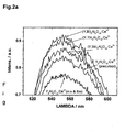
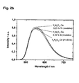
- the phosphors according to the invention have a higher luminous intensity compared to the non-co-doped YAG: Ce phosphors produced by solid-state diffusion methods (cf. FIGS. 1 and 2 ).
- the present invention thus provides phosphors with garnet structure of the formula II to IV (Y 1-xy Ce x Sb y ) 3 Al 5 O 12 with 0.005 ⁇ x ⁇ 0.1 and 0.001 ⁇ y ⁇ 0.005 (II) (Y 1 -xy Ce x Bi y ) 3 Al 5 O 12 with 0.005 sx ⁇ 0.1 and 0.001 ⁇ y ⁇ 0.005 (III) (Y 1-xy Ce x Th y ) 3 Al 5 O 12 with 0.005 ⁇ xs 0.1 and 0.001 ⁇ y ⁇ 0.005 (IV)
- the doping concentration of cerium is between 0.5 and 10 wt%. More preferably, it is between 2.0 and 5.0 wt%, and most preferably between 3.0 and 3.5 wt%. At a cerium concentration between 3.0 and 3.5%, there is generally an increased absorption and thus an increased light output or a greater brightness of the phosphor. A higher cerium concentration would reduce the quantum yield and in turn lead to a reduced light output.
- the absorption and emission spectrum, the thermal quenching behavior and the decay time ⁇ 1 / e luminescent materials according to the formula I depend strongly on the exact composition of the trivalent cations.
- Decisive for the above-mentioned spectroscopic properties is the crystal field strength of the dodecahedron position on the Ce 3+ or the covalent nature of the Ce-O bonds, ie the effective negative charge of the oxygen anions and the overlap of the anion and metal orbitals.
- the emission wavelength of the phosphor according to the invention is shifted to red. This is especially important for obtaining warm white light.
- a mixture of different phosphors namely a green-shifted phosphor, such as Y 3 (Al, Ga) 5 O 12 and the phosphor according to the invention, as well as a red phosphor (eg a red band or line emitter which can contribute a high lumen equivalent, such as europium-doped tungstates, molybdates and / or phosphates).
- blue-green phosphors can also be mixed in, for example Lu 3 Al 5 O 12 : Ce (LUAG: Ce). This results in an approximately continuous emission spectrum, which closely resembles the VIS daylight spectrum of the sun.
- the particle size of the phosphors according to the invention is between 50 nm and 30 .mu.m, preferably between 1 .mu.m and 20 .mu.m.
- the phosphor has a structured (eg pyramidal) surface on the side opposite an LED chip (see DE 102006054330.0 , Merck, which is incorporated by reference in its entirety in the context of the present application).
- a structured (eg pyramidal) surface on the side opposite an LED chip (see DE 102006054330.0 , Merck, which is incorporated by reference in its entirety in the context of the present application).
- the structured surface on the phosphor is prepared by subsequent coating with a suitable material, which is already structured, or in a subsequent step by (photo) lithographic Process, etching or by writing process with energy or matter beams or exposure to mechanical forces produced.
- the phosphors according to the invention have a rough surface on the side opposite to an LED chip, the nanoparticles of SiO 2 , TiO 2 , Al 2 O 3 , ZnO 2 , ZrO 2 and / or Y 2 O 3 or combinations of carries these materials or particles with the phosphor composition.
- a rough surface has a roughness of up to several 100 nm.
- the coated surface has the advantage that total reflection can be reduced or prevented and the light can be better decoupled from the phosphor according to the invention (see DE 102006054330.0 (Merck), which is incorporated by reference in its entirety in the context of the present application.)
- the phosphors according to the invention have a refractive index-matched layer on the surface facing away from the chip, which facilitates the decoupling of the primary radiation and / or the radiation emitted by the phosphor body.
- the phosphors have a closed surface coating consisting of SiO 2 , TiO 2 , Al 2 O 3 , ZnO, ZrO 2 and / or Y 2 O 3 or mixed oxides thereof.
- This surface coating has the advantage that an adaptation of the refractive index to the environment can be achieved by a suitable graduation of the refractive indices of the coating materials. In this case, the scattering of the light at the surface of the phosphor is reduced and a larger proportion of the light can penetrate into the phosphor where it is absorbed and converted.
- the refractive index matched surface coating allows more light to be coupled out of the phosphor because the total internal reflection is reduced.
- a closed layer is advantageous if the phosphor has to be encapsulated. This may be necessary to counter sensitivity of the phosphor or parts thereof to diffusing water or other materials in the immediate environment. Another reason for the encapsulation with a closed shell is a thermal decoupling of the actual phosphor from the heat that arises in the chip. This heat leads to a reduction in the fluorescent light output of the phosphor and may also affect the color of the fluorescent light. Finally, it is possible by such a coating to increase the efficiency of the phosphor by preventing lattice vibrations arising in the phosphor from propagating to the environment.
- the phosphors have a porous surface coating consisting of SiO 2 , TiO 2 , Al 2 O 3 , ZnO, ZrO 2 and / or Y 2 O 3 or mixed oxides thereof or of the phosphor composition.
- porous coatings offer the possibility of further reducing the refractive index of a single layer.
- the preparation of such porous coatings can be accomplished by three conventional methods as described in US Pat WO 03/027015 which is fully incorporated by reference into the context of the present application: the etching of glass (eg soda-lime glasses (see US 4,019,884 )), the application of a porous layer and the combination of porous layer and an etching process.
- the phosphors have a surface which carries functional groups which allows a chemical connection to the environment, preferably consisting of epoxy or silicone resin.
- functional groups may be, for example, esters bound via oxo groups or other derivatives which contain constituents of the binders based on epoxides and / or silicones Can enter shortcuts.
- Such surfaces have the advantage that a homogeneous mixing of the phosphors is made possible in the binder.
- the rheological properties of the system phosphor / binder and also the pot life can be adjusted to a certain extent. This simplifies the processing of the mixtures.
- the phosphor layer of the invention applied to the LED chip preferably consists of a mixture of silicone and homogeneous phosphor particles, and the silicone has a surface tension, this phosphor layer is not uniform at the microscopic level or the thickness of the layer is not consistently constant.
- Another object of the present invention is a phosphor with garnet structure obtainable by mixing aluminum, yttrium and cerium-containing educts with at least one antimony, bismuth, and / or thorium-containing co-dopant by wet chemical methods and subsequent thermal aftertreatment.
- the educts for producing the phosphor consist, as mentioned above, of the base material (eg salt solutions of aluminum, yttrium and cerium) and at least at least one Sb, Bi or Th-containing dopant.
- Suitable starting materials are inorganic and / or organic substances such as nitrates, carbonates, bicarbonates, phosphates, carboxylates, alcoholates, acetates, oxalates, halides, sulfates, organometallic compounds, hydroxides and / or oxides of metals, semimetals, transition metals and / or rare earths which dissolved in inorganic and / or organic liquids and / or are suspended.
- Preferably mixed nitrate solutions, chloride or hydroxide solutions are used which contain the corresponding elements in the required stoichiometric ratio.
- the wet-chemical preparation generally has the advantage over the conventional solid-state diffusion method that the resulting materials have a higher uniformity with regard to the stoichiometric composition, the particle size and the morphology of the particles from which the phosphor according to the invention is produced.
- nitrate solutions of the corresponding phosphorus are mixed with an NH 4 HCO 3 solution, whereby the phosphor precursor is formed.
- Spray pyrolysis belongs to the aerosol processes which are characterized by spraying solutions, suspensions or dispersions into a reaction chamber (reactor) which has been heated in different ways, as well as the formation and separation of solid particles.
- a reaction chamber reactor
- spray-drying with hot-gas temperatures ⁇ 200 ° C
- spray pyrolysis in addition to the evaporation of the solvent, the thermal decomposition of the educts used (eg salts) and the formation of new substances (eg oxides, mixed oxides ) instead of.
- the wet-chemical preparation of the phosphor preferably takes place by the precipitation and / or sol-gel process.
- the annealing at least partially under reducing conditions (For example, with carbon monoxide, forming gas, pure or hydrogen or at least vacuum or oxygen deficiency atmosphere) is performed.
- Methods can be made of any external forms of the phosphor particles, such as spherical particles, platelets, and patterned materials and ceramics.
- platelet-shaped phosphors as a further preferred embodiment is done by conventional methods from the corresponding metal and / or rare earth salts.
- the production process is in EP 763573 and DE 102006054331.9 described in detail which are fully incorporated by reference into the context of the present application.
- These platelet-shaped phosphors can be prepared by using a natural or synthetically produced highly stable support or a substrate of, for example mica, SiO 2 , Al 2 O 3 , ZrO 2 , glass or TiO 2 platelets, which is a very large Has aspect ratio, an atomically smooth surface and an adjustable thickness, can be coated by precipitation reaction in aqueous dispersion or suspension with a phosphor layer.
- the platelets may also consist of the phosphor material itself, or be composed of a material. If the wafer itself merely serves as a carrier for the phosphor coating, it must be made of a material which is transparent to the primary radiation of the LED, or absorbs the primary radiation and transfers this energy to the phosphor layer.
- the platelet-shaped phosphors are in a resin (eg Silicone or epoxy resin), and this dispersion is applied to the LED chip.
- the platelet-shaped phosphors can be produced on a large scale in thicknesses of 50 nm up to about 20 ⁇ m, preferably between 150 nm and 5 ⁇ m.
- the diameter is from 50 nm to 20 microns. It usually has an aspect ratio (ratio of diameter to particle thickness) of 1: 1 to 400: 1, and in particular 3: 1 to 100: 1.
- the platelet expansion (length x width) depends on the arrangement. Platelets are also suitable as scattering centers within the conversion layer, especially if they have particularly small dimensions.
- the surface of the platelet-shaped phosphor according to the invention facing the LED chip can be provided with a coating which acts in an anti-reflection manner with respect to the primary radiation emitted by the LED chip. This leads to a reduction in the backscattering of the primary radiation, as a result of which it can be better coupled into the phosphor body according to the invention.
- This coating can also consist of photonic crystals. This also includes a structuring of the surface of the platelet-shaped phosphor in order to achieve certain functionalities.
- the production of the phosphors according to the invention in the form of ceramic bodies is carried out analogously to that in the DE 102006037730 (Merck) described method fully incorporated by reference in the context of the present application.
- the phosphor is prepared wet-chemically by mixing the corresponding reactants and dopants, then isostatically pressed and in shape of a homogeneous thin and non-porous plate applied directly to the surface of the chip.
- no location-dependent variation of the excitation and emission of the phosphor takes place, as a result of which the LED equipped with it emits a homogeneous and color-constant light cone and has a high light output.
- the ceramic phosphor bodies can be produced industrially, for example, as platelets in thicknesses of a few 100 nm up to about 500 ⁇ m.
- the platelet extent (length x width) depends on the arrangement.
- the size of the wafer according to the chip size from about 100 .mu.m * 100 microns to several mm 2 ) with a certain excess of about 10% - 30% of the chip surface with a suitable chip arrangement (eg Flip Chip arrangement) or to choose accordingly. If the phosphor plate is placed over a finished LED, the emerging cone of light is completely covered by the plate.
- the side surfaces of the ceramic phosphor body can be mirrored with a light or noble metal, preferably aluminum or silver.
- the mirroring causes no light to emerge laterally from the phosphor body. Lateral exiting light can reduce the luminous flux to be coupled out of the LED.
- the mirroring of the ceramic phosphor body is carried out in a process step after the isostatic pressing to bars or plates, which may be done before the mirroring a tailor of the rods or plates in the required size.
- the side surfaces are for this purpose e.g. wetted with a solution of silver nitrate and glucose and then exposed at elevated temperature to an ammonia atmosphere.
- a silver coating on the side surfaces e.g. a silver coating on the side surfaces.
- the ceramic phosphor body can, if necessary, be fixed with a water glass solution on the substrate of an LED chip.
- the ceramic phosphor body has a structured (eg pyramidal) surface on the side opposite an LED chip.
- the structured surface on the phosphor body is produced in that in the isostatic pressing, the pressing tool has a structured pressing plate and thereby embossed a structure in the surface. Structured surfaces are desired when thin phosphor bodies or platelets are to be produced.
- the pressing conditions are known to the person skilled in the art (see J. Kriegsmann, Technical Ceramic Materials, Chap. 4, German Economic Service, 1998 ). It is important that 2/3 to 5/6 of the melting temperature of the material to be pressed are used as pressing temperatures.
- the excitability of the phosphors according to the invention also extend over a wide range, ranging from about 410 nm to 530 nm, preferably 430 nm to about 500 nm.
- these phosphors are not only suitable for excitation by UV or blue emitting primary light sources such as LEDs or conventional discharge lamps (eg based on Hg), but also for light sources such as those which exploit the blue In 3+ line at 451 nm.
- Another object of the present invention is a lighting unit with at least one primary light source whose emission maximum or maximum ranges in the range 410 nm to 530 nm, preferably 430 nm to about 500 nm. Particularly preferred is a range between 440 and 480 nm, wherein the primary radiation partially or completely by the inventive phosphors in longer wavelength radiation is converted.
- this lighting unit emits white or emits light with a certain color point (color-on-demand principle).
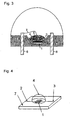
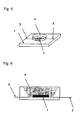
- Preferred embodiments of the lighting units according to the invention are in the FIGS. 3 to 14 shown.
- the light source is a luminescent arrangement based on ZnO, TCO (transparent conducting oxide), ZnSe or SiC or else an arrangement based on an organic light-emitting layer (OLED).
- the light source is a source which exhibits electroluminescence and / or photoluminescence.
- the light source may also be a plasma or discharge source.
- the phosphors according to the invention can either be dispersed in a resin (eg epoxy or silicone resin) or, with suitable size ratios, can be arranged directly on the primary light source or can be remotely located therefrom, depending on the application (the latter arrangement also includes “remote phosphor technology”). With one).
- a resin eg epoxy or silicone resin
- the advantages of "remote phosphor technology” are known to the person skilled in the art and can be found, for example, in the following publication: Japanese Journal. of Appl. Phys. Vol. 44, no. 21 (2005). L649-L651 ,
- the optical coupling of the illumination unit between the phosphor and the primary light source is realized by a light-conducting arrangement.
- the primary light source is installed at a central location and this is optically coupled to the phosphor by means of light-conducting devices, such as light-conducting fibers.
- the lighting requirements adapted lights can only be realized consisting of one or different phosphors, which can be arranged to form a luminescent screen, and a light guide, which is coupled to the primary light source realize.
- Another object of the present invention is the use of the phosphors according to the invention for the partial or complete conversion of blue or in the near UV emission of a light-emitting diode.
- the use of the phosphors according to the invention for the conversion of blue or near-UV emission into visible white radiation is preferred. Furthermore, the use of the phosphors according to the invention for converting the primary radiation into a specific color point according to the "color on demand" concept is preferred.
- Another object of the present invention is the use of the phosphors according to the invention in electroluminescent materials, such as electroluminescent films (also called phosphors or light foils) in which, for example, zinc sulfide or zinc sulfide doped with Mn 2+ , Cu + , or Ag + as an emitter is used, which emit in the yellow-green area.
- electroluminescent materials such as electroluminescent films (also called phosphors or light foils) in which, for example, zinc sulfide or zinc sulfide doped with Mn 2+ , Cu + , or Ag + as an emitter is used, which emit in the yellow-green area.
- the fields of application of the electroluminescent film are, for example, advertising, display backlighting in liquid crystal displays (LC displays) and thin-film transistor displays (TFT displays), self-illuminating license plate labels, floor graphics (in conjunction with a non-slip and non-slip laminate), in display and / or controls for example in automobiles, trains, ships and aircraft or household, gardening, measuring or sports and leisure equipment.
- LC displays liquid crystal displays
- TFT displays thin-film transistor displays
- license plate labels in conjunction with a non-slip and non-slip laminate
- floor graphics in conjunction with a non-slip and non-slip laminate
- Example 1 Preparation of the phosphor (Y 0.939 Ce 0.06 Th 0.001 ) 3 Al 5 O 12 by wet-chemical method
- ammonium bicarbonate 537.6 g are dissolved in 3 liters of deionized water.
- deionized water In about 400 ml of deionized water are 205.216 g of aluminum chloride hexahydrate, 151.522 g of yttrium chloride hexahydrate, 3.617 g of cerium chloride hexahydrate and 0.191 g of thorium (IV) chloride dissolved and rapidly added dropwise to the bicarbonate solution, while the pH by addition of conc. Ammonia are kept at pH 8. Then it is stirred for another hour. After aging, the precipitate is filtered off and dried in a drying oven at about 120 ° C.
- the dried precipitate is crushed and then calcined for 4 hours at 1000 ° C in air.
- the product is then resolidified and calcined at 1700 ° C. for 8 hours in a hydrogen / argon atmosphere.
- ammonium bicarbonate 537.6 g of ammonium bicarbonate are dissolved in 3 liters of deionized water.
- 205.216 g of aluminum chloride hexahydrate, 151.522 g of yttrium chloride hexahydrate, 3.617 g of cerium chloride hexahydrate and 0.161 g of bismuth (III) chloride are dissolved in about 400 ml of demineralized water and added dropwise rapidly to the bicarbonate solution, during which the pH must be low Addition of conc. Ammonia are kept at pH 8. Then it is stirred for another hour. After aging, the precipitate is filtered off and dried in a drying oven at about 120 ° C.
- the dried precipitate is crushed and then calcined for 4 hours at 1000 ° C in air.
- the product is then resolidified and calcined at 1700 ° C. for 8 hours in a hydrogen / argon atmosphere.
- Example 3 Preparation of the phosphor (Y 0.939 Ce 0.06 Sb 0.001 ) 3 Al 5 O 12 by wet-chemical method
- ammonium bicarbonate 537.6 g are dissolved in 3 liters of deionized water.
- deionized water In about 400 ml of deionized water are 205.216 g of aluminum chloride hexahydrate, 151.522 g of yttrium chloride hexahydrate, 3.617 g of cerium chloride hexahydrate and 0.116 g of antimony (III) chloride dissolved and rapidly added dropwise to the bicarbonate solution, while the pH by addition of conc. Ammonia are kept at pH 8. Then it is stirred for another hour. After aging, the precipitate is filtered off and dried in a drying oven at about 120 ° C.
- the dried precipitate is crushed and then calcined for 4 hours at 1000 ° C in air.
- the product is then resolidified and calcined at 1700 ° C. for 8 hours in a hydrogen / argon atmosphere.
- Example 4 Preparation of YAG: Ce (with Ce doping concentration 2%, Y 2.94 Al 5 O 12 : Ce 0.06 3+ ) according to the mixing & firing method (solid-state diffusion)
- cerium dioxide CeO 2
- Y 2 O 3 yttrium oxide
- Al 2 O 3 aluminum oxide
- the material is again finely ground and reductively calcined in the oven at a temperature of 1700 ° C over a period of 8 hours.
- Example 5 Preparation of YAG: Ce (with Ce doping concentration 2%, Y 2.94 Al 5 O 12 : Ce 0.06 3+ ) by the wet-chemical method
- ammonium bicarbonate 537.6 g of ammonium bicarbonate are dissolved in 3 liters of deionized water.
- deionized water 205.216 g of aluminum chloride hexahydrate, 153.242 g of yttrium chloride hexahydrate and 3.617 g of cerium chloride hexahydrate dissolved and rapidly added dropwise to the bicarbonate solution, while the pH by addition of conc. Ammonia are kept at pH 8. Then it is stirred for another hour. After aging, the precipitate is filtered off and dried in a drying oven at about 120 ° C.
- the dried precipitate is crushed and then calcined for 4 hours at 1000 ° C in air.
- the product is then resolidified and calcined at 1700 ° C for 8 hours in a hydrogen argon atmosphere.
- the samples are characterized by X-ray powder diffraction, luminescence and reflection spectroscopy.
Landscapes
- Chemical & Material Sciences (AREA)
- Engineering & Computer Science (AREA)
- Inorganic Chemistry (AREA)
- Materials Engineering (AREA)
- Organic Chemistry (AREA)
- Nanotechnology (AREA)
- Crystallography & Structural Chemistry (AREA)
- Manufacturing & Machinery (AREA)
- Luminescent Compositions (AREA)
- Vessels And Coating Films For Discharge Lamps (AREA)
- Glass Compositions (AREA)
- Developing Agents For Electrophotography (AREA)
- Catalysts (AREA)
Applications Claiming Priority (2)
| Application Number | Priority Date | Filing Date | Title |
|---|---|---|---|
| DE102007010719A DE102007010719A1 (de) | 2007-03-06 | 2007-03-06 | Leuchtstoffe bestehend aus dotierten Granaten für pcLEDs |
| PCT/EP2008/001074 WO2008107062A1 (de) | 2007-03-06 | 2008-02-13 | Leuchtstoffe bestehend aus dotierten granaten für pcleds |
Publications (2)
| Publication Number | Publication Date |
|---|---|
| EP2115092A1 EP2115092A1 (de) | 2009-11-11 |
| EP2115092B1 true EP2115092B1 (de) | 2011-05-04 |
Family
ID=39429885
Family Applications (1)
| Application Number | Title | Priority Date | Filing Date |
|---|---|---|---|
| EP08707688A Not-in-force EP2115092B1 (de) | 2007-03-06 | 2008-02-13 | Leuchtstoffe bestehend aus dotierten granaten für pcleds |
Country Status (9)
Families Citing this family (55)
| Publication number | Priority date | Publication date | Assignee | Title |
|---|---|---|---|---|
| US8529791B2 (en) * | 2006-10-20 | 2013-09-10 | Intematix Corporation | Green-emitting, garnet-based phosphors in general and backlighting applications |
| JP2009110737A (ja) * | 2007-10-29 | 2009-05-21 | Citizen Electronics Co Ltd | 照明装置及びその製造方法 |
| DE102007053285A1 (de) * | 2007-11-08 | 2009-05-14 | Merck Patent Gmbh | Verfahren zur Herstellung von beschichteten Leuchtstoffen |
| JP2009120405A (ja) * | 2007-11-09 | 2009-06-04 | Canon Inc | 紫外光用ガラス組成物及びそれを用いた光学装置 |
| DE102007053770A1 (de) * | 2007-11-12 | 2009-05-14 | Merck Patent Gmbh | Beschichtete Leuchtstoffpartikel mit Brechungsindex-Anpassung |
| CN101712871B (zh) * | 2008-10-06 | 2013-01-02 | 罗维鸿 | 白光发光二极管及其碘化物石榴石荧光粉 |
| DE102008051029A1 (de) * | 2008-10-13 | 2010-04-15 | Merck Patent Gmbh | Dotierte Granat-Leuchtstoffe mit Rotverschiebung für pcLEDs |
| DE102008058621A1 (de) * | 2008-11-22 | 2010-05-27 | Merck Patent Gmbh | Co-dotierte 1-1-2-Nitride |
| JP5156841B2 (ja) * | 2009-04-17 | 2013-03-06 | パナソニック株式会社 | 蛍光体、発光装置およびプラズマディスプレイパネル |
| DE102009025266B4 (de) * | 2009-06-17 | 2015-08-20 | Osram Opto Semiconductors Gmbh | Optoelektronisches Halbleiterbauteil |
| DE102009050542A1 (de) | 2009-10-23 | 2011-04-28 | Merck Patent Gmbh | Sm-aktivierte Aluminat- und Borat-Leuchtstoffe |
| KR20120101172A (ko) * | 2010-05-18 | 2012-09-12 | 파나소닉 주식회사 | 플라즈마 디스플레이 패널 및 녹색 형광체층 |
| JP5189211B2 (ja) * | 2010-07-20 | 2013-04-24 | パナソニック株式会社 | 電球形ランプ |
| CN101914381B (zh) * | 2010-08-13 | 2013-06-12 | 西安创联电气科技(集团)有限责任公司 | 黄色荧光粉及其制备方法 |
| JP5674385B2 (ja) * | 2010-08-27 | 2015-02-25 | 古河機械金属株式会社 | シンチレータ用ガーネット型結晶およびこれを用いる放射線検出器 |
| WO2012046642A1 (ja) * | 2010-10-05 | 2012-04-12 | 株式会社ネモト・ルミマテリアル | 緑色系発光蛍光体および発光装置 |
| CN102010715B (zh) * | 2010-10-21 | 2013-06-05 | 罗维鸿 | 用于暖白光led的荧光粉 |
| DE112011104985T5 (de) * | 2011-03-01 | 2014-01-16 | Osram Gmbh | Beleuchtungsvorrichtung mit Leuchtstoffelement |
| US20130092964A1 (en) * | 2011-10-13 | 2013-04-18 | Intematix Corporation | Highly reliable photoluminescent materials having a thick and uniform titanium dioxide coating |
| CN103045267B (zh) * | 2011-10-17 | 2014-11-26 | 有研稀土新材料股份有限公司 | 一种氮化物荧光粉、其制备方法及含该荧光粉的发光装置 |
| US9006966B2 (en) | 2011-11-08 | 2015-04-14 | Intematix Corporation | Coatings for photoluminescent materials |
| US20130143334A1 (en) * | 2011-12-01 | 2013-06-06 | Hung Ta Trading Co., Ltd. | Method of enhancing color rendering index of a white led |
| EP2607449B1 (en) * | 2011-12-22 | 2014-04-02 | Shin-Etsu Chemical Co., Ltd. | Preparation of yttrium-cerium-aluminum garnet phosphor |
| WO2013143645A1 (de) * | 2012-03-29 | 2013-10-03 | Merck Patent Gmbh | Kompositkeramik, die einen konversionsleuchtstoff und ein mit einem negativen thermischen ausdehnungskoeffizienten material enthält |
| CN103375708B (zh) * | 2012-04-26 | 2015-10-28 | 展晶科技(深圳)有限公司 | 发光二极管灯源装置 |
| DE102012107797A1 (de) * | 2012-08-23 | 2014-02-27 | Osram Opto Semiconductors Gmbh | Verfahren zur Herstellung eines Licht emittierenden Halbleiterbauelements und Licht emittierendes Halbleiterbauelement |
| TWI597349B (zh) * | 2012-09-21 | 2017-09-01 | 住友大阪水泥股份有限公司 | 複合波長變換粉體、含有複合波長變換粉體的樹脂組成物及發光裝置 |
| KR101249444B1 (ko) * | 2012-10-25 | 2013-04-03 | 주식회사 포스포 | 토륨이 도핑된 가넷계 형광체 및 이를 이용한 발광장치 |
| CN103232847A (zh) * | 2013-01-23 | 2013-08-07 | 苏州大学 | 一种led用锑酸盐红色荧光粉及其制备方法 |
| CN103952153A (zh) * | 2014-05-21 | 2014-07-30 | 烟台建塬光电技术有限公司 | 掺杂Lu、Sb的铝酸盐绿色荧光粉及其制备方法 |
| WO2016056837A1 (ko) * | 2014-10-08 | 2016-04-14 | 서울반도체 주식회사 | 발광 장치 |
| US9580650B1 (en) * | 2014-12-25 | 2017-02-28 | DM Lighting Technologies Inc. | Method of manufacturing Ce:YAG polycrystalline phosphor |
| KR101633421B1 (ko) * | 2015-06-08 | 2016-06-24 | 주식회사 포스포 | 세륨이 도핑된 가넷계 형광체, 이의 제조방법 및 이를 이용한 발광소자 |
| CN108337918B (zh) * | 2015-07-02 | 2021-07-09 | 亮锐控股有限公司 | 波长转换发光设备 |
| DE102015213460A1 (de) | 2015-07-17 | 2017-01-19 | Osram Gmbh | Wellenlängenumwandlung von Primärlicht mittels eines Konversionskörpers |
| DE102015213858A1 (de) | 2015-07-22 | 2017-01-26 | Osram Gmbh | Beleuchtungsvorrichtung |
| JP6680868B2 (ja) | 2015-08-17 | 2020-04-15 | インフィニット アースロスコピー インコーポレーテッド, リミテッド | 光源 |
| KR101778563B1 (ko) | 2015-09-25 | 2017-09-18 | 세종대학교산학협력단 | 루테튬 알루미늄 가넷계 형광체 분말 및 이의 제조 방법 |
| US11330963B2 (en) | 2015-11-16 | 2022-05-17 | Lazurite Holdings Llc | Wireless medical imaging system |
| US10253257B2 (en) | 2015-11-25 | 2019-04-09 | Intematix Corporation | Coated narrow band red phosphor |
| JP6555111B2 (ja) | 2015-12-09 | 2019-08-07 | 日亜化学工業株式会社 | ハイブリッド蛍光体の製造方法及びハイブリッド蛍光体 |
| US10982141B2 (en) | 2015-12-23 | 2021-04-20 | Lg Innotek Co., Ltd. | Phosphor composition, light-emitting device package comprising same, and lighting apparatus |
| KR101755283B1 (ko) | 2016-01-14 | 2017-07-10 | 한국화학연구원 | 형광체 제조 방법 및 이에 제조되는 형광체 |
| WO2018079421A1 (ja) * | 2016-10-28 | 2018-05-03 | 日本特殊陶業株式会社 | 光波長変換部材及び発光装置 |
| JP6597657B2 (ja) * | 2017-01-24 | 2019-10-30 | 日亜化学工業株式会社 | 発光装置 |
| MX2019009715A (es) | 2017-02-15 | 2020-01-27 | Infinite Arthroscopy Inc Ltd | Sistema medico inalambrico de formacion de imagen que comprende unidad de cabezal y cable de luz que comprende fuente luminosa integrada. |
| WO2019053242A1 (de) | 2017-09-18 | 2019-03-21 | Merck Patent Gmbh | Mehrkomponentenleuchtstoffe als farbkonverter für festkörperlichtquellen |
| DE102018200023A1 (de) | 2018-01-02 | 2019-07-04 | Osram Gmbh | Konversionsvorrichtung mit geschichteter leiterstruktur |
| JP7030333B2 (ja) * | 2018-04-23 | 2022-03-07 | 国立大学法人神戸大学 | Uvb領域の紫外発光蛍光体および紫外発光デバイス |
| US11254865B2 (en) | 2018-08-10 | 2022-02-22 | Osram Opto Semiconductors Gmbh | Process of manufacturing a conversion element, conversion element and light emitting device comprising the conversion element |
| USD938584S1 (en) | 2020-03-30 | 2021-12-14 | Lazurite Holdings Llc | Hand piece |
| USD972176S1 (en) | 2020-08-06 | 2022-12-06 | Lazurite Holdings Llc | Light source |
| CN111908910B (zh) * | 2020-08-18 | 2022-04-22 | 新沂市锡沂高新材料产业技术研究院有限公司 | 一种暖白光照明用高显指透明陶瓷及其制备方法 |
| RU2746650C1 (ru) * | 2020-09-11 | 2021-04-19 | Федеральное государственное бюджетное учреждение науки Институт химии твердого тела Уральского отделения Российской академии наук | Сложный оксид алюминия и редкоземельных элементов и способ его получения |
| EP4198105A1 (en) * | 2021-12-16 | 2023-06-21 | Seaborough IP I B.V. | Microjet reactor based synthesis of nanophosphors |
Family Cites Families (35)
| Publication number | Priority date | Publication date | Assignee | Title |
|---|---|---|---|---|
| US4019884A (en) | 1976-01-22 | 1977-04-26 | Corning Glass Works | Method for providing porous broad-band antireflective surface layers on chemically-durable borosilicate glasses |
| US4550256A (en) | 1983-10-17 | 1985-10-29 | At&T Bell Laboratories | Visual display system utilizing high luminosity single crystal garnet material |
| JP3242561B2 (ja) | 1995-09-14 | 2001-12-25 | メルク・ジヤパン株式会社 | 薄片状酸化アルミニウム、真珠光沢顔料及びその製造方法 |
| US6652967B2 (en) * | 2001-08-08 | 2003-11-25 | Nanoproducts Corporation | Nano-dispersed powders and methods for their manufacture |
| WO2001008452A1 (de) * | 1999-07-23 | 2001-02-01 | Patent-Treuhand-Gesellschaft für elektrische Glühlampen mbH | Leuchstoff für lichtquellen und zugehörige lichtquelle |
| DE19951790A1 (de) | 1999-10-27 | 2001-05-03 | Patent Treuhand Ges Fuer Elektrische Gluehlampen Mbh | Leuchtstoff für Lichtquellen und zugehörige Lichtquelle |
| US6552487B1 (en) * | 1999-10-27 | 2003-04-22 | Patent-Treuhand-Gesellschaft Fuer Elektrische Gluehlampen Mbh | Phosphor for light sources, and associated light source |
| US6700322B1 (en) | 2000-01-27 | 2004-03-02 | General Electric Company | Light source with organic layer and photoluminescent layer |
| DE10009915A1 (de) * | 2000-03-01 | 2001-09-27 | Philips Corp Intellectual Pty | Plasmabildschirm mit UV-Licht emittierender Schicht |
| DE10010638A1 (de) * | 2000-03-03 | 2001-09-13 | Osram Opto Semiconductors Gmbh | Verfahren zur Herstellung eines lichtabstrahlenden Halbleiterkörpers mit Lumineszenzkonversionselement |
| US6596195B2 (en) * | 2001-06-01 | 2003-07-22 | General Electric Company | Broad-spectrum terbium-containing garnet phosphors and white-light sources incorporating the same |
| DE10129630A1 (de) * | 2001-06-20 | 2003-01-02 | Philips Corp Intellectual Pty | Niederdruckgasentladungslampe mit Leuchtstoffbeschichtung |
| TWI287569B (en) * | 2001-06-27 | 2007-10-01 | Nantex Industry Co Ltd | Yttrium aluminium garnet fluorescent powder comprising at least two optical active center, its preparation and uses |
| KR100913641B1 (ko) | 2001-09-21 | 2009-08-24 | 메르크 파텐트 게엠베하 | 내마모성 sio2 반사방지 층을 제조하기 위한 신규하이브리드 졸 |
| US7541005B2 (en) * | 2001-09-26 | 2009-06-02 | Siemens Energy Inc. | Catalytic thermal barrier coatings |
| JP4932107B2 (ja) * | 2001-09-28 | 2012-05-16 | 株式会社ファインラバー研究所 | 発光装置 |
| US6903505B2 (en) * | 2001-12-17 | 2005-06-07 | General Electric Company | Light-emitting device with organic electroluminescent material and photoluminescent materials |
| KR100983193B1 (ko) * | 2002-03-22 | 2010-09-20 | 니치아 카가쿠 고교 가부시키가이샤 | 질화물 형광체와 그 제조 방법 및 발광 장치 |
| TWI226357B (en) * | 2002-05-06 | 2005-01-11 | Osram Opto Semiconductors Gmbh | Wavelength-converting reaction-resin, its production method, light-radiating optical component and light-radiating semiconductor-body |
| US6870311B2 (en) * | 2002-06-07 | 2005-03-22 | Lumileds Lighting U.S., Llc | Light-emitting devices utilizing nanoparticles |
| US7015640B2 (en) * | 2002-09-11 | 2006-03-21 | General Electric Company | Diffusion barrier coatings having graded compositions and devices incorporating the same |
| US7544309B2 (en) | 2002-12-13 | 2009-06-09 | Koninklijke Philips Electronics N.V. | Illumination system comprising a radiation source and a fluorescent material |
| US7038370B2 (en) * | 2003-03-17 | 2006-05-02 | Lumileds Lighting, U.S., Llc | Phosphor converted light emitting device |
| DE10360546A1 (de) | 2003-12-22 | 2005-07-14 | Patent-Treuhand-Gesellschaft für elektrische Glühlampen mbH | Leuchtstoff und Lichtquelle mit derartigem Leuchtstoff |
| US20050164019A1 (en) * | 2004-01-22 | 2005-07-28 | General Electric Company | Charge transfer-promoting materials and electronic devices incorporating same |
| WO2006006099A1 (en) | 2004-07-05 | 2006-01-19 | Philips Intellectual Property & Standards Gmbh | Illumination system comprising a radiation source and a fluorescent material |
| JP2006165266A (ja) * | 2004-12-07 | 2006-06-22 | Matsushita Electric Works Ltd | 発光装置 |
| US7671529B2 (en) * | 2004-12-10 | 2010-03-02 | Philips Lumileds Lighting Company, Llc | Phosphor converted light emitting device |
| CN100566490C (zh) * | 2005-03-14 | 2009-12-02 | 皇家飞利浦电子股份有限公司 | 多晶陶瓷结构中的磷光体和包括该磷光体的发光元件 |
| CN100487934C (zh) * | 2005-04-08 | 2009-05-13 | 日亚化学工业株式会社 | 具有由丝网印刷形成的有机硅树脂层的发光器件 |
| DE102006027133A1 (de) | 2006-06-12 | 2007-12-13 | Merck Patent Gmbh | Verfahren zur Herstellung von Granat-Leuchtstoffen in einem Pulsationsreaktor |
| DE102006037730A1 (de) | 2006-08-11 | 2008-02-14 | Merck Patent Gmbh | LED-Konversionsleuchtstoffe in Form von keramischen Körpern |
| DE102006054331A1 (de) | 2006-11-17 | 2008-05-21 | Merck Patent Gmbh | Leuchtstoffkörper basierend auf plättchenförmigen Substraten |
| DE102006054330A1 (de) * | 2006-11-17 | 2008-05-21 | Merck Patent Gmbh | Leuchtstoffplättchen für LEDs aus strukturierten Folien |
| CN101838536B (zh) * | 2010-04-09 | 2012-08-22 | 佛山市南海区大沥朗达荧光材料有限公司 | 白光led用yag荧光粉及其制造方法 |
-
2007
- 2007-03-06 DE DE102007010719A patent/DE102007010719A1/de not_active Withdrawn
-
2008
- 2008-02-13 WO PCT/EP2008/001074 patent/WO2008107062A1/de active Application Filing
- 2008-02-13 US US12/530,075 patent/US8088304B2/en not_active Expired - Fee Related
- 2008-02-13 JP JP2009552084A patent/JP5313173B2/ja not_active Expired - Fee Related
- 2008-02-13 CN CN200880007397XA patent/CN101641425B/zh not_active Expired - Fee Related
- 2008-02-13 AT AT08707688T patent/ATE508178T1/de active
- 2008-02-13 KR KR1020097020806A patent/KR101487040B1/ko not_active Expired - Fee Related
- 2008-02-13 EP EP08707688A patent/EP2115092B1/de not_active Not-in-force
- 2008-02-13 DE DE502008003422T patent/DE502008003422D1/de active Active
- 2008-03-06 TW TW097107946A patent/TWI462991B/zh not_active IP Right Cessation
Also Published As
| Publication number | Publication date |
|---|---|
| EP2115092A1 (de) | 2009-11-11 |
| DE502008003422D1 (de) | 2011-06-16 |
| TW200902685A (en) | 2009-01-16 |
| KR101487040B1 (ko) | 2015-01-28 |
| CN101641425A (zh) | 2010-02-03 |
| DE102007010719A1 (de) | 2008-09-11 |
| JP5313173B2 (ja) | 2013-10-09 |
| CN101641425B (zh) | 2013-05-01 |
| JP2010520337A (ja) | 2010-06-10 |
| TWI462991B (zh) | 2014-12-01 |
| US20100084962A1 (en) | 2010-04-08 |
| US8088304B2 (en) | 2012-01-03 |
| WO2008107062A1 (de) | 2008-09-12 |
| KR20100015388A (ko) | 2010-02-12 |
| ATE508178T1 (de) | 2011-05-15 |
Similar Documents
| Publication | Publication Date | Title |
|---|---|---|
| EP2115092B1 (de) | Leuchtstoffe bestehend aus dotierten granaten für pcleds | |
| WO2010043287A1 (de) | Dotierte granat-leuchtstoffe mit rotverschiebung für pcleds | |
| EP2129740B1 (de) | Verfahren zur herstellung von leuchtstoffen basierend auf orthosilikaten für pcleds | |
| EP2616523B1 (de) | Silicophosphat-leuchtstoffe | |
| EP2129741B1 (de) | VERFAHREN ZUR HERSTELLUNG VON LEUCHTSTOFFEN BESTEHEND AUS ORTHOSILIKATEN FÜR pcLEDs | |
| EP2401342B1 (de) | Mit zirkonium und hafnium co-dotierte nitridosilikate | |
| EP2207866B1 (de) | Beschichtete leuchtstoffpartikel mit brechungsindex-anpassung | |
| EP2596078B1 (de) | Aluminat-leuchtstoffe | |
| EP2324096B1 (de) | Co-dotierte 1-1-2 nitride | |
| DE102007053285A1 (de) | Verfahren zur Herstellung von beschichteten Leuchtstoffen | |
| DE102009032711A1 (de) | Co-dotierte Silicooxynitride | |
| EP2625247B1 (de) | Mn-aktivierte leuchtstoffe | |
| WO2011047757A1 (de) | Sm-aktivierte aluminat- und borat-leuchtstoffe | |
| DE102010031914A1 (de) | Carbodiimid-Leuchtstoffe |
Legal Events
| Date | Code | Title | Description |
|---|---|---|---|
| PUAI | Public reference made under article 153(3) epc to a published international application that has entered the european phase |
Free format text: ORIGINAL CODE: 0009012 |
|
| 17P | Request for examination filed |
Effective date: 20090710 |
|
| AK | Designated contracting states |
Kind code of ref document: A1 Designated state(s): AT BE BG CH CY CZ DE DK EE ES FI FR GB GR HR HU IE IS IT LI LT LU LV MC MT NL NO PL PT RO SE SI SK TR |
|
| 17Q | First examination report despatched |
Effective date: 20100317 |
|
| DAX | Request for extension of the european patent (deleted) | ||
| GRAP | Despatch of communication of intention to grant a patent |
Free format text: ORIGINAL CODE: EPIDOSNIGR1 |
|
| RTI1 | Title (correction) |
Free format text: LUMINOPHORES MADE OF DOPED GARNETS FOR PCLEDS |
|
| GRAS | Grant fee paid |
Free format text: ORIGINAL CODE: EPIDOSNIGR3 |
|
| GRAA | (expected) grant |
Free format text: ORIGINAL CODE: 0009210 |
|
| AK | Designated contracting states |
Kind code of ref document: B1 Designated state(s): AT BE BG CH CY CZ DE DK EE ES FI FR GB GR HR HU IE IS IT LI LT LU LV MC MT NL NO PL PT RO SE SI SK TR |
|
| REG | Reference to a national code |
Ref country code: GB Ref legal event code: FG4D Free format text: NOT ENGLISH |
|
| REG | Reference to a national code |
Ref country code: CH Ref legal event code: EP |
|
| REG | Reference to a national code |
Ref country code: IE Ref legal event code: FG4D Free format text: LANGUAGE OF EP DOCUMENT: GERMAN |
|
| REF | Corresponds to: |
Ref document number: 502008003422 Country of ref document: DE Date of ref document: 20110616 Kind code of ref document: P |
|
| REG | Reference to a national code |
Ref country code: DE Ref legal event code: R096 Ref document number: 502008003422 Country of ref document: DE Effective date: 20110616 |
|
| REG | Reference to a national code |
Ref country code: NL Ref legal event code: T3 |
|
| PG25 | Lapsed in a contracting state [announced via postgrant information from national office to epo] |
Ref country code: LT Free format text: LAPSE BECAUSE OF FAILURE TO SUBMIT A TRANSLATION OF THE DESCRIPTION OR TO PAY THE FEE WITHIN THE PRESCRIBED TIME-LIMIT Effective date: 20110504 Ref country code: PT Free format text: LAPSE BECAUSE OF FAILURE TO SUBMIT A TRANSLATION OF THE DESCRIPTION OR TO PAY THE FEE WITHIN THE PRESCRIBED TIME-LIMIT Effective date: 20110905 Ref country code: NO Free format text: LAPSE BECAUSE OF FAILURE TO SUBMIT A TRANSLATION OF THE DESCRIPTION OR TO PAY THE FEE WITHIN THE PRESCRIBED TIME-LIMIT Effective date: 20110804 Ref country code: SE Free format text: LAPSE BECAUSE OF FAILURE TO SUBMIT A TRANSLATION OF THE DESCRIPTION OR TO PAY THE FEE WITHIN THE PRESCRIBED TIME-LIMIT Effective date: 20110504 |
|
| PG25 | Lapsed in a contracting state [announced via postgrant information from national office to epo] |
Ref country code: SI Free format text: LAPSE BECAUSE OF FAILURE TO SUBMIT A TRANSLATION OF THE DESCRIPTION OR TO PAY THE FEE WITHIN THE PRESCRIBED TIME-LIMIT Effective date: 20110504 Ref country code: IS Free format text: LAPSE BECAUSE OF FAILURE TO SUBMIT A TRANSLATION OF THE DESCRIPTION OR TO PAY THE FEE WITHIN THE PRESCRIBED TIME-LIMIT Effective date: 20110904 Ref country code: FI Free format text: LAPSE BECAUSE OF FAILURE TO SUBMIT A TRANSLATION OF THE DESCRIPTION OR TO PAY THE FEE WITHIN THE PRESCRIBED TIME-LIMIT Effective date: 20110504 Ref country code: ES Free format text: LAPSE BECAUSE OF FAILURE TO SUBMIT A TRANSLATION OF THE DESCRIPTION OR TO PAY THE FEE WITHIN THE PRESCRIBED TIME-LIMIT Effective date: 20110815 Ref country code: GR Free format text: LAPSE BECAUSE OF FAILURE TO SUBMIT A TRANSLATION OF THE DESCRIPTION OR TO PAY THE FEE WITHIN THE PRESCRIBED TIME-LIMIT Effective date: 20110805 Ref country code: CY Free format text: LAPSE BECAUSE OF FAILURE TO SUBMIT A TRANSLATION OF THE DESCRIPTION OR TO PAY THE FEE WITHIN THE PRESCRIBED TIME-LIMIT Effective date: 20110504 Ref country code: LV Free format text: LAPSE BECAUSE OF FAILURE TO SUBMIT A TRANSLATION OF THE DESCRIPTION OR TO PAY THE FEE WITHIN THE PRESCRIBED TIME-LIMIT Effective date: 20110504 |
|
| REG | Reference to a national code |
Ref country code: IE Ref legal event code: FD4D |
|
| PG25 | Lapsed in a contracting state [announced via postgrant information from national office to epo] |
Ref country code: CZ Free format text: LAPSE BECAUSE OF FAILURE TO SUBMIT A TRANSLATION OF THE DESCRIPTION OR TO PAY THE FEE WITHIN THE PRESCRIBED TIME-LIMIT Effective date: 20110504 Ref country code: IE Free format text: LAPSE BECAUSE OF FAILURE TO SUBMIT A TRANSLATION OF THE DESCRIPTION OR TO PAY THE FEE WITHIN THE PRESCRIBED TIME-LIMIT Effective date: 20110504 Ref country code: EE Free format text: LAPSE BECAUSE OF FAILURE TO SUBMIT A TRANSLATION OF THE DESCRIPTION OR TO PAY THE FEE WITHIN THE PRESCRIBED TIME-LIMIT Effective date: 20110504 |
|
| PG25 | Lapsed in a contracting state [announced via postgrant information from national office to epo] |
Ref country code: DK Free format text: LAPSE BECAUSE OF FAILURE TO SUBMIT A TRANSLATION OF THE DESCRIPTION OR TO PAY THE FEE WITHIN THE PRESCRIBED TIME-LIMIT Effective date: 20110504 Ref country code: RO Free format text: LAPSE BECAUSE OF FAILURE TO SUBMIT A TRANSLATION OF THE DESCRIPTION OR TO PAY THE FEE WITHIN THE PRESCRIBED TIME-LIMIT Effective date: 20110504 Ref country code: SK Free format text: LAPSE BECAUSE OF FAILURE TO SUBMIT A TRANSLATION OF THE DESCRIPTION OR TO PAY THE FEE WITHIN THE PRESCRIBED TIME-LIMIT Effective date: 20110504 Ref country code: PL Free format text: LAPSE BECAUSE OF FAILURE TO SUBMIT A TRANSLATION OF THE DESCRIPTION OR TO PAY THE FEE WITHIN THE PRESCRIBED TIME-LIMIT Effective date: 20110504 |
|
| PLBE | No opposition filed within time limit |
Free format text: ORIGINAL CODE: 0009261 |
|
| STAA | Information on the status of an ep patent application or granted ep patent |
Free format text: STATUS: NO OPPOSITION FILED WITHIN TIME LIMIT |
|
| 26N | No opposition filed |
Effective date: 20120207 |
|
| PG25 | Lapsed in a contracting state [announced via postgrant information from national office to epo] |
Ref country code: IT Free format text: LAPSE BECAUSE OF FAILURE TO SUBMIT A TRANSLATION OF THE DESCRIPTION OR TO PAY THE FEE WITHIN THE PRESCRIBED TIME-LIMIT Effective date: 20110504 Ref country code: HR Free format text: LAPSE BECAUSE OF FAILURE TO SUBMIT A TRANSLATION OF THE DESCRIPTION OR TO PAY THE FEE WITHIN THE PRESCRIBED TIME-LIMIT Effective date: 20111123 |
|
| REG | Reference to a national code |
Ref country code: DE Ref legal event code: R097 Ref document number: 502008003422 Country of ref document: DE Effective date: 20120207 |
|
| BERE | Be: lapsed |
Owner name: MERCK PATENT G.M.B.H. Effective date: 20120228 |
|
| PG25 | Lapsed in a contracting state [announced via postgrant information from national office to epo] |
Ref country code: MC Free format text: LAPSE BECAUSE OF NON-PAYMENT OF DUE FEES Effective date: 20120229 |
|
| REG | Reference to a national code |
Ref country code: CH Ref legal event code: PL |
|
| PG25 | Lapsed in a contracting state [announced via postgrant information from national office to epo] |
Ref country code: LI Free format text: LAPSE BECAUSE OF NON-PAYMENT OF DUE FEES Effective date: 20120229 Ref country code: CH Free format text: LAPSE BECAUSE OF NON-PAYMENT OF DUE FEES Effective date: 20120229 |
|
| REG | Reference to a national code |
Ref country code: FR Ref legal event code: ST Effective date: 20121031 |
|
| PG25 | Lapsed in a contracting state [announced via postgrant information from national office to epo] |
Ref country code: BE Free format text: LAPSE BECAUSE OF NON-PAYMENT OF DUE FEES Effective date: 20120228 |
|
| PG25 | Lapsed in a contracting state [announced via postgrant information from national office to epo] |
Ref country code: FR Free format text: LAPSE BECAUSE OF NON-PAYMENT OF DUE FEES Effective date: 20120229 |
|
| PG25 | Lapsed in a contracting state [announced via postgrant information from national office to epo] |
Ref country code: BG Free format text: LAPSE BECAUSE OF FAILURE TO SUBMIT A TRANSLATION OF THE DESCRIPTION OR TO PAY THE FEE WITHIN THE PRESCRIBED TIME-LIMIT Effective date: 20110804 |
|
| PG25 | Lapsed in a contracting state [announced via postgrant information from national office to epo] |
Ref country code: MT Free format text: LAPSE BECAUSE OF FAILURE TO SUBMIT A TRANSLATION OF THE DESCRIPTION OR TO PAY THE FEE WITHIN THE PRESCRIBED TIME-LIMIT Effective date: 20110504 |
|
| PG25 | Lapsed in a contracting state [announced via postgrant information from national office to epo] |
Ref country code: HR Free format text: LAPSE BECAUSE OF FAILURE TO SUBMIT A TRANSLATION OF THE DESCRIPTION OR TO PAY THE FEE WITHIN THE PRESCRIBED TIME-LIMIT Effective date: 20110504 |
|
| REG | Reference to a national code |
Ref country code: AT Ref legal event code: MM01 Ref document number: 508178 Country of ref document: AT Kind code of ref document: T Effective date: 20130213 |
|
| PG25 | Lapsed in a contracting state [announced via postgrant information from national office to epo] |
Ref country code: TR Free format text: LAPSE BECAUSE OF FAILURE TO SUBMIT A TRANSLATION OF THE DESCRIPTION OR TO PAY THE FEE WITHIN THE PRESCRIBED TIME-LIMIT Effective date: 20110504 |
|
| PG25 | Lapsed in a contracting state [announced via postgrant information from national office to epo] |
Ref country code: LU Free format text: LAPSE BECAUSE OF NON-PAYMENT OF DUE FEES Effective date: 20120213 Ref country code: AT Free format text: LAPSE BECAUSE OF NON-PAYMENT OF DUE FEES Effective date: 20130213 |
|
| PG25 | Lapsed in a contracting state [announced via postgrant information from national office to epo] |
Ref country code: HU Free format text: LAPSE BECAUSE OF FAILURE TO SUBMIT A TRANSLATION OF THE DESCRIPTION OR TO PAY THE FEE WITHIN THE PRESCRIBED TIME-LIMIT Effective date: 20080213 |
|
| PGFP | Annual fee paid to national office [announced via postgrant information from national office to epo] |
Ref country code: NL Payment date: 20160111 Year of fee payment: 9 |
|
| PGFP | Annual fee paid to national office [announced via postgrant information from national office to epo] |
Ref country code: DE Payment date: 20160209 Year of fee payment: 9 |
|
| REG | Reference to a national code |
Ref country code: DE Ref legal event code: R119 Ref document number: 502008003422 Country of ref document: DE |
|
| REG | Reference to a national code |
Ref country code: NL Ref legal event code: MM Effective date: 20170301 |
|
| PG25 | Lapsed in a contracting state [announced via postgrant information from national office to epo] |
Ref country code: NL Free format text: LAPSE BECAUSE OF NON-PAYMENT OF DUE FEES Effective date: 20170301 |
|
| PG25 | Lapsed in a contracting state [announced via postgrant information from national office to epo] |
Ref country code: DE Free format text: LAPSE BECAUSE OF NON-PAYMENT OF DUE FEES Effective date: 20170901 |
|
| PGFP | Annual fee paid to national office [announced via postgrant information from national office to epo] |
Ref country code: GB Payment date: 20180207 Year of fee payment: 11 |
|
| GBPC | Gb: european patent ceased through non-payment of renewal fee |
Effective date: 20190213 |
|
| PG25 | Lapsed in a contracting state [announced via postgrant information from national office to epo] |
Ref country code: GB Free format text: LAPSE BECAUSE OF NON-PAYMENT OF DUE FEES Effective date: 20190213 |