JP5313173B2 - pcLEDのためのドープしたガーネット製の発光団 - Google Patents
pcLEDのためのドープしたガーネット製の発光団 Download PDFInfo
- Publication number
- JP5313173B2 JP5313173B2 JP2009552084A JP2009552084A JP5313173B2 JP 5313173 B2 JP5313173 B2 JP 5313173B2 JP 2009552084 A JP2009552084 A JP 2009552084A JP 2009552084 A JP2009552084 A JP 2009552084A JP 5313173 B2 JP5313173 B2 JP 5313173B2
- Authority
- JP
- Japan
- Prior art keywords
- phosphor
- light source
- zno
- primary light
- phosphors
- Prior art date
- Legal status (The legal status is an assumption and is not a legal conclusion. Google has not performed a legal analysis and makes no representation as to the accuracy of the status listed.)
- Expired - Fee Related
Links
Images


Classifications
-
- C—CHEMISTRY; METALLURGY
- C09—DYES; PAINTS; POLISHES; NATURAL RESINS; ADHESIVES; COMPOSITIONS NOT OTHERWISE PROVIDED FOR; APPLICATIONS OF MATERIALS NOT OTHERWISE PROVIDED FOR
- C09K—MATERIALS FOR MISCELLANEOUS APPLICATIONS, NOT PROVIDED FOR ELSEWHERE
- C09K11/00—Luminescent, e.g. electroluminescent, chemiluminescent materials
- C09K11/08—Luminescent, e.g. electroluminescent, chemiluminescent materials containing inorganic luminescent materials
- C09K11/77—Luminescent, e.g. electroluminescent, chemiluminescent materials containing inorganic luminescent materials containing rare earth metals
- C09K11/7766—Luminescent, e.g. electroluminescent, chemiluminescent materials containing inorganic luminescent materials containing rare earth metals containing two or more rare earth metals
- C09K11/7774—Aluminates
-
- B—PERFORMING OPERATIONS; TRANSPORTING
- B82—NANOTECHNOLOGY
- B82B—NANOSTRUCTURES FORMED BY MANIPULATION OF INDIVIDUAL ATOMS, MOLECULES, OR LIMITED COLLECTIONS OF ATOMS OR MOLECULES AS DISCRETE UNITS; MANUFACTURE OR TREATMENT THEREOF
- B82B3/00—Manufacture or treatment of nanostructures by manipulation of individual atoms or molecules, or limited collections of atoms or molecules as discrete units
-
- C—CHEMISTRY; METALLURGY
- C09—DYES; PAINTS; POLISHES; NATURAL RESINS; ADHESIVES; COMPOSITIONS NOT OTHERWISE PROVIDED FOR; APPLICATIONS OF MATERIALS NOT OTHERWISE PROVIDED FOR
- C09K—MATERIALS FOR MISCELLANEOUS APPLICATIONS, NOT PROVIDED FOR ELSEWHERE
- C09K11/00—Luminescent, e.g. electroluminescent, chemiluminescent materials
- C09K11/08—Luminescent, e.g. electroluminescent, chemiluminescent materials containing inorganic luminescent materials
- C09K11/77—Luminescent, e.g. electroluminescent, chemiluminescent materials containing inorganic luminescent materials containing rare earth metals
-
- C—CHEMISTRY; METALLURGY
- C09—DYES; PAINTS; POLISHES; NATURAL RESINS; ADHESIVES; COMPOSITIONS NOT OTHERWISE PROVIDED FOR; APPLICATIONS OF MATERIALS NOT OTHERWISE PROVIDED FOR
- C09K—MATERIALS FOR MISCELLANEOUS APPLICATIONS, NOT PROVIDED FOR ELSEWHERE
- C09K11/00—Luminescent, e.g. electroluminescent, chemiluminescent materials
- C09K11/08—Luminescent, e.g. electroluminescent, chemiluminescent materials containing inorganic luminescent materials
- C09K11/88—Luminescent, e.g. electroluminescent, chemiluminescent materials containing inorganic luminescent materials containing selenium, tellurium or unspecified chalcogen elements
-
- H—ELECTRICITY
- H01—ELECTRIC ELEMENTS
- H01L—SEMICONDUCTOR DEVICES NOT COVERED BY CLASS H10
- H01L2224/00—Indexing scheme for arrangements for connecting or disconnecting semiconductor or solid-state bodies and methods related thereto as covered by H01L24/00
- H01L2224/01—Means for bonding being attached to, or being formed on, the surface to be connected, e.g. chip-to-package, die-attach, "first-level" interconnects; Manufacturing methods related thereto
- H01L2224/42—Wire connectors; Manufacturing methods related thereto
- H01L2224/47—Structure, shape, material or disposition of the wire connectors after the connecting process
- H01L2224/48—Structure, shape, material or disposition of the wire connectors after the connecting process of an individual wire connector
- H01L2224/4805—Shape
- H01L2224/4809—Loop shape
- H01L2224/48091—Arched
-
- H—ELECTRICITY
- H01—ELECTRIC ELEMENTS
- H01L—SEMICONDUCTOR DEVICES NOT COVERED BY CLASS H10
- H01L2224/00—Indexing scheme for arrangements for connecting or disconnecting semiconductor or solid-state bodies and methods related thereto as covered by H01L24/00
- H01L2224/01—Means for bonding being attached to, or being formed on, the surface to be connected, e.g. chip-to-package, die-attach, "first-level" interconnects; Manufacturing methods related thereto
- H01L2224/42—Wire connectors; Manufacturing methods related thereto
- H01L2224/47—Structure, shape, material or disposition of the wire connectors after the connecting process
- H01L2224/48—Structure, shape, material or disposition of the wire connectors after the connecting process of an individual wire connector
- H01L2224/481—Disposition
- H01L2224/48151—Connecting between a semiconductor or solid-state body and an item not being a semiconductor or solid-state body, e.g. chip-to-substrate, chip-to-passive
- H01L2224/48221—Connecting between a semiconductor or solid-state body and an item not being a semiconductor or solid-state body, e.g. chip-to-substrate, chip-to-passive the body and the item being stacked
- H01L2224/48245—Connecting between a semiconductor or solid-state body and an item not being a semiconductor or solid-state body, e.g. chip-to-substrate, chip-to-passive the body and the item being stacked the item being metallic
- H01L2224/48257—Connecting between a semiconductor or solid-state body and an item not being a semiconductor or solid-state body, e.g. chip-to-substrate, chip-to-passive the body and the item being stacked the item being metallic connecting the wire to a die pad of the item
-
- H—ELECTRICITY
- H01—ELECTRIC ELEMENTS
- H01L—SEMICONDUCTOR DEVICES NOT COVERED BY CLASS H10
- H01L2224/00—Indexing scheme for arrangements for connecting or disconnecting semiconductor or solid-state bodies and methods related thereto as covered by H01L24/00
- H01L2224/01—Means for bonding being attached to, or being formed on, the surface to be connected, e.g. chip-to-package, die-attach, "first-level" interconnects; Manufacturing methods related thereto
- H01L2224/42—Wire connectors; Manufacturing methods related thereto
- H01L2224/47—Structure, shape, material or disposition of the wire connectors after the connecting process
- H01L2224/49—Structure, shape, material or disposition of the wire connectors after the connecting process of a plurality of wire connectors
- H01L2224/491—Disposition
- H01L2224/49105—Connecting at different heights
- H01L2224/49107—Connecting at different heights on the semiconductor or solid-state body
-
- H—ELECTRICITY
- H01—ELECTRIC ELEMENTS
- H01L—SEMICONDUCTOR DEVICES NOT COVERED BY CLASS H10
- H01L2224/00—Indexing scheme for arrangements for connecting or disconnecting semiconductor or solid-state bodies and methods related thereto as covered by H01L24/00
- H01L2224/73—Means for bonding being of different types provided for in two or more of groups H01L2224/10, H01L2224/18, H01L2224/26, H01L2224/34, H01L2224/42, H01L2224/50, H01L2224/63, H01L2224/71
- H01L2224/732—Location after the connecting process
- H01L2224/73251—Location after the connecting process on different surfaces
- H01L2224/73265—Layer and wire connectors
-
- H—ELECTRICITY
- H01—ELECTRIC ELEMENTS
- H01L—SEMICONDUCTOR DEVICES NOT COVERED BY CLASS H10
- H01L2224/00—Indexing scheme for arrangements for connecting or disconnecting semiconductor or solid-state bodies and methods related thereto as covered by H01L24/00
- H01L2224/80—Methods for connecting semiconductor or other solid state bodies using means for bonding being attached to, or being formed on, the surface to be connected
- H01L2224/85—Methods for connecting semiconductor or other solid state bodies using means for bonding being attached to, or being formed on, the surface to be connected using a wire connector
- H01L2224/85909—Post-treatment of the connector or wire bonding area
- H01L2224/8592—Applying permanent coating, e.g. protective coating
-
- H—ELECTRICITY
- H01—ELECTRIC ELEMENTS
- H01L—SEMICONDUCTOR DEVICES NOT COVERED BY CLASS H10
- H01L2924/00—Indexing scheme for arrangements or methods for connecting or disconnecting semiconductor or solid-state bodies as covered by H01L24/00
- H01L2924/10—Details of semiconductor or other solid state devices to be connected
- H01L2924/11—Device type
- H01L2924/12—Passive devices, e.g. 2 terminal devices
- H01L2924/1204—Optical Diode
- H01L2924/12044—OLED
-
- H—ELECTRICITY
- H01—ELECTRIC ELEMENTS
- H01L—SEMICONDUCTOR DEVICES NOT COVERED BY CLASS H10
- H01L2924/00—Indexing scheme for arrangements or methods for connecting or disconnecting semiconductor or solid-state bodies as covered by H01L24/00
- H01L2924/15—Details of package parts other than the semiconductor or other solid state devices to be connected
- H01L2924/181—Encapsulation
-
- H—ELECTRICITY
- H01—ELECTRIC ELEMENTS
- H01L—SEMICONDUCTOR DEVICES NOT COVERED BY CLASS H10
- H01L33/00—Semiconductor devices with at least one potential-jump barrier or surface barrier specially adapted for light emission; Processes or apparatus specially adapted for the manufacture or treatment thereof or of parts thereof; Details thereof
- H01L33/48—Semiconductor devices with at least one potential-jump barrier or surface barrier specially adapted for light emission; Processes or apparatus specially adapted for the manufacture or treatment thereof or of parts thereof; Details thereof characterised by the semiconductor body packages
- H01L33/50—Wavelength conversion elements
- H01L33/501—Wavelength conversion elements characterised by the materials, e.g. binder
- H01L33/502—Wavelength conversion materials
Description
・蛍光体の表面は、大きい比率の一次放射を散乱し、これは、この比率が蛍光体により吸収され得ないことを意味する、
・イオン、特に活性剤イオン(activator ion)が蛍光体粒子中に不均一に分布する結果、内部量子収量の減少がもたらされる、
EP-1095 998には、組成A3B5O12:(Ce,Pr)を有し、ここでAが群Y、Tb、Laおよび/またはLuからの希土類金属であり、BがAlおよび/またはGaを意味する蛍光体が開示されている。
WO 2005/061659には、A3B5O12(Ce,Pr,Eu)タイプのガーネット構造を有し、ここでA=希土類金属であり、B=Al、Gaであり、ここで成分BのいくらかがSiにより置き換えられている蛍光体が記載されている。
(Ya,Gdb,Luc,Sed,Sme,Tbf,Prg,Thh,Iri,Sbj,Bik)3−x(All,Gam)5O12:Cex (I)
式中、
a+b+c+d+e+f+g+h+i+j+k=1であり、
l+m=1であり、
x=0.005〜0.1である、
で表されるガーネット構造を有する蛍光体に関する。
(Y1−x−yCexSby)3Al5O12、式中0.005≦x≦0.1および0.001≦y≦0.005 (II)
(Y1−x−yCexBiy)3Al5O12、式中0.005≦x≦0.1および0.001≦y≦0.005 (III)
(Y1−x−yCexThy)3Al5O12、式中0.005≦x≦0.1および0.001≦y≦0.005 (IV)
酸化物、モリブデン酸塩、タングステン酸塩、バナジウム酸塩、III族窒化物、(オキシ)窒化物、各々個々に、または1種もしくは2種以上の活性剤イオン、例えばCe、Eu、Mn、Crおよび/またはBiとのこれらの混合物。
特定の色空間が確立されるべきである場合には、これは特に有利である。
a)Sb、Biおよび/またはTh含有物質で同時ドープされたセリウムで活性化された蛍光体を、蛍光体前駆体懸濁液または溶液から、Y、Al、Ce、Gd、Lu、Sc、Sm、Tb、Prおよび/またはGa含有物質から選択される少なくとも3種の出発物質を湿式化学的方法により混合することにより調製すること、
b)Sb、Biおよび/またはThで同時ドープされた蛍光体を熱後処理すること
を有する蛍光体の製造方法に関する。
・クエン酸およびエチレングリコールの溶液を用いるPecchini法(例えばAnnual Review of Materials Research Vol. 36: 2006, 281-331を参照)
・尿素を用いる燃焼法
・水溶液または有機塩溶液(出発物質)の噴霧乾燥
・水溶液または有機塩溶液(出発物質)の噴霧熱分解
・硝酸塩溶液の蒸発および残留物の熱変換
1)構成成分を均一に沈殿させ、次に溶媒を分離し、続いて単一段階の、または多段階の熱後処理を施し、ここでこれらの段階の1つを還元雰囲気中で行ってもよい、
2)例えば噴霧プロセスの補助により、混合物を微細に分割し、溶媒を除去し、続いて単一段階の、または多段階の熱後処理を施し、ここでこれらの段階の1つを還元雰囲気中で行ってもよい、あるいは、
4)その後、方法1〜3の補助により調製した蛍光体をコーティングして、これらの環境への屈折率適合を達成する。
前述の熱後処理において、か焼を、還元条件(例えば一酸化炭素、フォーミングガス、純粋な水素または少なくとも真空であるかもしくは酸素欠乏雰囲気を用いる)下で少なくとも部分的に行うのが、好ましい。
前述の方法により、蛍光体粒子のすべての所望の外形、例えば球状粒子、薄片または構造化された材料およびセラミックスを作製するのが可能になる。
これは、一般的に、1:1〜400:1、特に3:1〜100:1のアスペクト比(直径対粒子の厚さの比率)を有する。
薄片の大きさ(長さ×幅)は、配置に依存する。薄片はまた、特にこれらが特に小さい寸法を有する場合には、変換層内の散乱の中心部としても適する。
セラミックス蛍光体素子を、所要に応じて、水ガラス溶液を用いてLEDチップの基板に固定することができる。
本発明の蛍光体を、さらに、好ましくは、青色または近UV発光を可視白色放射に変換するために用いる。本発明の蛍光体を、さらに、好ましくは、「カラーオンデマンド」概念によって一次放射を特定の色点に変換するために用いる。
例1:湿式化学的方法による蛍光体(Y0.939Ce0.06Th0.001)3Al5O12の調製
537.6gの炭酸水素アンモニウムを、3リットルの脱イオン水に溶解する。205.216gの塩化アルミニウム六水和物、151.522gの塩化イットリウム六水和物、3.617gの塩化セリウム六水和物および0.191gの塩化トリウム(IV)を、約400mlの脱イオン水に溶解し、炭酸水素溶液に迅速に滴加する。この添加の間、濃アンモニアを加えることにより、pHをpH 8に維持しなければならない。その後、混合物を、さらに1時間撹拌する。熟成させた後、沈殿物を濾別し、乾燥キャビネット中で約120℃にて乾燥する。
537.6gの炭酸水素アンモニウムを、3リットルの脱イオン水に溶解する。205.216gの塩化アルミニウム六水和物、151.522gの塩化イットリウム六水和物、3.617gの塩化セリウム六水和物および0.161gの塩化ビスマス(III)を、約400mlの脱イオン水に溶解し、炭酸水素溶液に迅速に滴加する。この添加の間、濃アンモニアを加えることにより、pHをpH 8に維持しなければならない。その後、混合物を、さらに1時間撹拌する。熟成させた後、沈殿物を濾別し、乾燥キャビネット中で約120℃にて乾燥する。
537.6gの炭酸水素アンモニウムを、3リットルの脱イオン水に溶解する。205.216gの塩化アルミニウム六水和物、151.522gの塩化イットリウム六水和物、3.617gの塩化セリウム六水和物および0.116gの塩化アンチモン(III)を、約400mlの脱イオン水に溶解し、炭酸水素溶液に迅速に滴加する。この添加の間、濃アンモニアを加えることにより、pHをpH 8に維持しなければならない。その後、混合物を、さらに1時間撹拌する。熟成させた後、沈殿物を濾別し、乾燥キャビネット中で約120℃にて乾燥する。
0.344gの二酸化セリウム(CeO2)、33.646gの酸化イットリウム(Y2O3)および25.491gの酸化アルミニウム(Al2O3)を秤量し、水でスラリーにする。この混合物を、乳鉢中で少量の水を用いることにより湿式粉砕する。次に、スラリーを、チャンバー炉中に移送し、ここでこれを、フォーミングガス雰囲気中で1200℃の温度にて6時間にわたりか焼する。冷却後、材料を再び微細に粉砕し、これに、炉中で1700℃の温度にて8時間にわたり、還元的か焼を施す。
537.6gの炭酸水素アンモニウムを、3リットルの脱イオン水に溶解する。205.216gの塩化アルミニウム六水和物、153.242gの塩化イットリウム六水和物および3.617gの塩化セリウム六水和物を、約400mlの脱イオン水に溶解し、炭酸水素溶液に迅速に滴加する。この添加の間、濃アンモニアを加えることにより、pHをpH 8に維持しなければならない。その後、混合物を、さらに1時間撹拌する。熟成させた後、沈殿物を濾別し、乾燥キャビネット中で約120℃にて乾燥する。
12.5mmolのガンマ−酸化アルミニウムAl2O3、7.35mmol−xの酸化イットリウムY2O3、0.3mmolの二酸化セリウムCeO2および0.015mmol≦x≦0.075mmolの酸化トリウムThO2を、秤量する。その後、出発物質をアセトンでスラリーにし、乳鉢中で十分に粉砕する。最初のか焼段階において、試料を、1200℃にて一酸化炭素の下で2時間加熱する。乳鉢中でさらに十分に粉砕した後、第2のか焼段階を行い、ここで、バッチを、1650℃にて、同様に一酸化炭素雰囲気下で4時間加熱する。
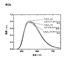
(Y0.969Ce0.02X0.001)3Al5O12、
ここでX=Sb:(x/y)=0.438/0.541、
ここでX=Bi:(x/y)=0.440/0.539、
ここでX=Th:(x/y)=0.439/0.541
固体拡散反応により調製された商業的なYAG:Ce:
(x/y)=0.435/0.541
湿式化学的方法により調製されたYAG:Ce:
(x/y)=0.435/0.541
Claims (22)
- ガーネット構造を有する蛍光体であって、式II〜IV:
(Y1−x−yCexSby)3Al5O12、式中0.005≦x≦0.1および0.001≦y≦0.005 (II)
(Y1−x−yCexBiy)3Al5O12、式中0.005≦x≦0.1および0.001≦y≦0.005 (III)
(Y1−x−yCexThy)3Al5O12、式中0.005≦x≦0.1および0.001≦y≦0.005 (IV)
で表される化合物から選択される化合物であることを特徴とする、前記蛍光体。 - SiO2、TiO2、Al2O3、ZnO、ZrO2および/またはY2O3もしくはこれらの混合酸化物のナノ粒子または蛍光体組成物を含む粒子を担持する表面を有することを特徴とする、請求項1に記載の蛍光体。
- SiO2、TiO2、Al2O3、ZnO、ZrO2および/またはY2O3またはこれらの混合酸化物からなる連続的表面コーティングを有することを特徴とする、請求項1または2に記載の蛍光体。
- SiO2、TiO2、Al2O3、ZnO、ZrO2および/またはY2O3またはこれらの混合酸化物または蛍光体組成物からなる多孔性表面コーティングを有することを特徴とする、請求項1〜3のいずれか一項に記載の蛍光体。
- 表面が、エポキシまたはシリコーン樹脂からなる、周囲との化学結合を促進する官能基を担持することを特徴とする、請求項1〜4のいずれか一項に記載の蛍光体。
- アルミニウム、イットリウムおよびセリウム含有出発物質と、少なくとも1種のSb、Biおよび/またはTh含有同時ドーパントとを、湿式化学的方法により混合し、その後熱処理することにより得られる、請求項1〜5のいずれか一項に記載の蛍光体。
- 下記の式II〜IVで表されるガーネット構造を有する蛍光体の製造方法であって、
(Y 1−x−y Ce x Sb y ) 3 Al 5 O 12 、式中0.005≦x≦0.1および0.001≦y≦0.005 (II)
(Y 1−x−y Ce x Bi y ) 3 Al 5 O 12 、式中0.005≦x≦0.1および0.001≦y≦0.005 (III)
(Y 1−x−y Ce x Th y ) 3 Al 5 O 12 、式中0.005≦x≦0.1および0.001≦y≦0.005 (IV)
以下のプロセス段階:
a)アンチモン、ビスマスおよび/またはトリウム含有物質で同時ドープされたセリウム活性化蛍光体を、蛍光体前駆体懸濁液または溶液から、Y含有物質、Al含有物質、およびCe含有物質から選択される少なくとも3種の出発物質を湿式化学的方法により混合することによって調製すること、
b)アンチモン、ビスマスおよび/またはトリウムで同時ドープされた蛍光体を熱後処理すること
を有する、前記方法。 - 蛍光体前駆体を、段階a)において、ゾル−ゲル法、沈殿・乾燥法、および/または噴霧乾燥法により、有機および/または無機金属および/または希土類元素塩から湿式化学的方法により調製することを特徴とする、請求項7に記載の方法。
- 蛍光体の表面が、SiO2、TiO2、Al2O3、ZnO、ZrO2および/またはY2O3もしくはこれらの混合酸化物のナノ粒子または蛍光体組成物のナノ粒子で被覆されていることを特徴とする、請求項7または8に記載の方法。
- 蛍光体の表面が、SiO2、TiO2、Al2O3、ZnO、ZrO2および/またはY2O3またはこれらの混合酸化物の連続的コーティングを備えることを特徴とする、請求項7または8に記載の方法。
- 蛍光体の表面が、SiO2、TiO2、Al2O3、ZnO、ZrO2および/またはY2O3またはこれらの混合酸化物または蛍光体組成物の多孔性コーティングを備えることを特徴とする、請求項7または8に記載の方法。
- 発光極大が410nm〜530nmの範囲内にある少なくとも1種の一次光源を有する照明ユニットであって、この放射が、請求項1〜6のいずれか一項に記載の蛍光体によってより長い波長の放射に部分的に、または完全に変換される、前記照明ユニット。
- 一次光源が、式In i Ga j Al k N(式中0≦i、0≦j、0≦k、およびi+j+k=1)で表されるルミネッセンス性の窒化インジウムアルミニウムガリウムであることを特徴とする、請求項12に記載の照明ユニット。
- 一次光源が、ZnO、TCO(透明伝導性酸化物)、ZnSeもしくはSiCをベースとするルミネッセンス化合物であることを特徴とする、請求項12に記載の照明ユニット。
- 一次光源が、有機発光層をベースとする材料であることを特徴とする、請求項12に記載の照明ユニット。
- 一次光源が、エレクトロルミネッセンスおよび/またはフォトルミネッセンスを示す光源であることを特徴とする、請求項12に記載の照明ユニット。
- 一次光源が、プラズマまたは放電源であることを特徴とする、請求項12に記載の照明ユニット。
- 蛍光体を、一次光源上に直接配置するか、および/またはこれから遠隔に配置することを特徴とする、請求項12〜17のいずれか一項に記載の照明ユニット。
- 蛍光体と一次光源との間の光学的結合が、光伝導性の配置により達成されることを特徴とする、請求項12〜18のいずれか一項に記載の照明ユニット。
- 請求項1〜6のいずれか一項に記載の蛍光体のうち、少なくとも1種の蛍光体の、発光ダイオードからの青色または近UV発光を部分的に、または完全に変換するための変換蛍光体としての使用。
- 請求項1〜6のいずれか一項に記載の蛍光体のうち、少なくとも1種の蛍光体の、カラーオンデマンド概念によって一次放射を特定の色点に変換するための変換蛍光体としての使用。
- 請求項1〜6のいずれか一項に記載の蛍光体のうち、少なくとも1種の蛍光体の、青色または近UV発光を可視白色放射に変換するための使用。
Applications Claiming Priority (3)
| Application Number | Priority Date | Filing Date | Title |
|---|---|---|---|
| DE102007010719.8 | 2007-03-06 | ||
| DE102007010719A DE102007010719A1 (de) | 2007-03-06 | 2007-03-06 | Leuchtstoffe bestehend aus dotierten Granaten für pcLEDs |
| PCT/EP2008/001074 WO2008107062A1 (de) | 2007-03-06 | 2008-02-13 | Leuchtstoffe bestehend aus dotierten granaten für pcleds |
Publications (3)
| Publication Number | Publication Date |
|---|---|
| JP2010520337A JP2010520337A (ja) | 2010-06-10 |
| JP2010520337A5 JP2010520337A5 (ja) | 2011-03-31 |
| JP5313173B2 true JP5313173B2 (ja) | 2013-10-09 |
Family
ID=39429885
Family Applications (1)
| Application Number | Title | Priority Date | Filing Date |
|---|---|---|---|
| JP2009552084A Expired - Fee Related JP5313173B2 (ja) | 2007-03-06 | 2008-02-13 | pcLEDのためのドープしたガーネット製の発光団 |
Country Status (9)
| Country | Link |
|---|---|
| US (1) | US8088304B2 (ja) |
| EP (1) | EP2115092B1 (ja) |
| JP (1) | JP5313173B2 (ja) |
| KR (1) | KR101487040B1 (ja) |
| CN (1) | CN101641425B (ja) |
| AT (1) | ATE508178T1 (ja) |
| DE (2) | DE102007010719A1 (ja) |
| TW (1) | TWI462991B (ja) |
| WO (1) | WO2008107062A1 (ja) |
Cited By (1)
| Publication number | Priority date | Publication date | Assignee | Title |
|---|---|---|---|---|
| US11001756B2 (en) | 2015-12-09 | 2021-05-11 | Nichia Corporation | Method of producing hybrid fluorescent material |
Families Citing this family (54)
| Publication number | Priority date | Publication date | Assignee | Title |
|---|---|---|---|---|
| US8529791B2 (en) * | 2006-10-20 | 2013-09-10 | Intematix Corporation | Green-emitting, garnet-based phosphors in general and backlighting applications |
| JP2009110737A (ja) * | 2007-10-29 | 2009-05-21 | Citizen Electronics Co Ltd | 照明装置及びその製造方法 |
| DE102007053285A1 (de) * | 2007-11-08 | 2009-05-14 | Merck Patent Gmbh | Verfahren zur Herstellung von beschichteten Leuchtstoffen |
| JP2009120405A (ja) * | 2007-11-09 | 2009-06-04 | Canon Inc | 紫外光用ガラス組成物及びそれを用いた光学装置 |
| DE102007053770A1 (de) * | 2007-11-12 | 2009-05-14 | Merck Patent Gmbh | Beschichtete Leuchtstoffpartikel mit Brechungsindex-Anpassung |
| CN101712871B (zh) * | 2008-10-06 | 2013-01-02 | 罗维鸿 | 白光发光二极管及其碘化物石榴石荧光粉 |
| DE102008051029A1 (de) * | 2008-10-13 | 2010-04-15 | Merck Patent Gmbh | Dotierte Granat-Leuchtstoffe mit Rotverschiebung für pcLEDs |
| DE102008058621A1 (de) | 2008-11-22 | 2010-05-27 | Merck Patent Gmbh | Co-dotierte 1-1-2-Nitride |
| JP5156841B2 (ja) * | 2009-04-17 | 2013-03-06 | パナソニック株式会社 | 蛍光体、発光装置およびプラズマディスプレイパネル |
| DE102009025266B4 (de) * | 2009-06-17 | 2015-08-20 | Osram Opto Semiconductors Gmbh | Optoelektronisches Halbleiterbauteil |
| DE102009050542A1 (de) * | 2009-10-23 | 2011-04-28 | Merck Patent Gmbh | Sm-aktivierte Aluminat- und Borat-Leuchtstoffe |
| CN102754180A (zh) * | 2010-05-18 | 2012-10-24 | 松下电器产业株式会社 | 等离子显示面板及绿色荧光体层 |
| WO2012011279A1 (ja) * | 2010-07-20 | 2012-01-26 | パナソニック株式会社 | 電球形ランプ |
| CN101914381B (zh) * | 2010-08-13 | 2013-06-12 | 西安创联电气科技(集团)有限责任公司 | 黄色荧光粉及其制备方法 |
| JP5674385B2 (ja) * | 2010-08-27 | 2015-02-25 | 古河機械金属株式会社 | シンチレータ用ガーネット型結晶およびこれを用いる放射線検出器 |
| JP5669855B2 (ja) * | 2010-10-05 | 2015-02-18 | 株式会社ネモト・ルミマテリアル | 緑色系発光蛍光体および発光装置 |
| CN102010715B (zh) * | 2010-10-21 | 2013-06-05 | 罗维鸿 | 用于暖白光led的荧光粉 |
| CN103403438A (zh) * | 2011-03-01 | 2013-11-20 | 欧司朗股份有限公司 | 具有荧光元件的照明设备 |
| US20130092964A1 (en) * | 2011-10-13 | 2013-04-18 | Intematix Corporation | Highly reliable photoluminescent materials having a thick and uniform titanium dioxide coating |
| CN103045267B (zh) * | 2011-10-17 | 2014-11-26 | 有研稀土新材料股份有限公司 | 一种氮化物荧光粉、其制备方法及含该荧光粉的发光装置 |
| US9006966B2 (en) | 2011-11-08 | 2015-04-14 | Intematix Corporation | Coatings for photoluminescent materials |
| US20130143334A1 (en) * | 2011-12-01 | 2013-06-06 | Hung Ta Trading Co., Ltd. | Method of enhancing color rendering index of a white led |
| EP2607449B1 (en) * | 2011-12-22 | 2014-04-02 | Shin-Etsu Chemical Co., Ltd. | Preparation of yttrium-cerium-aluminum garnet phosphor |
| CN107324795A (zh) * | 2012-03-29 | 2017-11-07 | 默克专利有限公司 | 包含转化磷光体和具有负的热膨胀系数的材料的复合陶瓷 |
| CN103375708B (zh) * | 2012-04-26 | 2015-10-28 | 展晶科技(深圳)有限公司 | 发光二极管灯源装置 |
| DE102012107797A1 (de) * | 2012-08-23 | 2014-02-27 | Osram Opto Semiconductors Gmbh | Verfahren zur Herstellung eines Licht emittierenden Halbleiterbauelements und Licht emittierendes Halbleiterbauelement |
| TWI597349B (zh) * | 2012-09-21 | 2017-09-01 | 住友大阪水泥股份有限公司 | 複合波長變換粉體、含有複合波長變換粉體的樹脂組成物及發光裝置 |
| KR101249444B1 (ko) * | 2012-10-25 | 2013-04-03 | 주식회사 포스포 | 토륨이 도핑된 가넷계 형광체 및 이를 이용한 발광장치 |
| CN103232847A (zh) * | 2013-01-23 | 2013-08-07 | 苏州大学 | 一种led用锑酸盐红色荧光粉及其制备方法 |
| CN103952153A (zh) * | 2014-05-21 | 2014-07-30 | 烟台建塬光电技术有限公司 | 掺杂Lu、Sb的铝酸盐绿色荧光粉及其制备方法 |
| CN110055059B (zh) | 2014-10-08 | 2022-12-27 | 首尔半导体株式会社 | 发光装置 |
| US9580650B1 (en) * | 2014-12-25 | 2017-02-28 | DM Lighting Technologies Inc. | Method of manufacturing Ce:YAG polycrystalline phosphor |
| KR101633421B1 (ko) * | 2015-06-08 | 2016-06-24 | 주식회사 포스포 | 세륨이 도핑된 가넷계 형광체, 이의 제조방법 및 이를 이용한 발광소자 |
| JP6890556B2 (ja) * | 2015-07-02 | 2021-06-18 | ルミレッズ ホールディング ベーフェー | 波長変換発光デバイス |
| DE102015213460A1 (de) | 2015-07-17 | 2017-01-19 | Osram Gmbh | Wellenlängenumwandlung von Primärlicht mittels eines Konversionskörpers |
| DE102015213858A1 (de) | 2015-07-22 | 2017-01-26 | Osram Gmbh | Beleuchtungsvorrichtung |
| JP6680868B2 (ja) | 2015-08-17 | 2020-04-15 | インフィニット アースロスコピー インコーポレーテッド, リミテッド | 光源 |
| KR101778563B1 (ko) | 2015-09-25 | 2017-09-18 | 세종대학교산학협력단 | 루테튬 알루미늄 가넷계 형광체 분말 및 이의 제조 방법 |
| US11330963B2 (en) | 2015-11-16 | 2022-05-17 | Lazurite Holdings Llc | Wireless medical imaging system |
| US10253257B2 (en) | 2015-11-25 | 2019-04-09 | Intematix Corporation | Coated narrow band red phosphor |
| WO2017111495A1 (ko) * | 2015-12-23 | 2017-06-29 | 엘지이노텍 주식회사 | 형광체 조성물, 이를 포함하는 발광 소자 패키지 및 조명 장치 |
| KR101755283B1 (ko) | 2016-01-14 | 2017-07-10 | 한국화학연구원 | 형광체 제조 방법 및 이에 제조되는 형광체 |
| EP3534193B1 (en) * | 2016-10-28 | 2021-12-22 | Ngk Spark Plug Co., Ltd. | Optical wavelength conversion member and light-emitting device |
| JP6597657B2 (ja) | 2017-01-24 | 2019-10-30 | 日亜化学工業株式会社 | 発光装置 |
| US10610089B2 (en) | 2017-02-15 | 2020-04-07 | Infinite Arthroscopy, Inc. Limited | Wireless imaging system comprising a head unit and a light cable that comprises an integrated light source |
| WO2019053242A1 (de) | 2017-09-18 | 2019-03-21 | Merck Patent Gmbh | Mehrkomponentenleuchtstoffe als farbkonverter für festkörperlichtquellen |
| DE102018200023A1 (de) | 2018-01-02 | 2019-07-04 | Osram Gmbh | Konversionsvorrichtung mit geschichteter leiterstruktur |
| JP7030333B2 (ja) * | 2018-04-23 | 2022-03-07 | 国立大学法人神戸大学 | Uvb領域の紫外発光蛍光体および紫外発光デバイス |
| US11254865B2 (en) | 2018-08-10 | 2022-02-22 | Osram Opto Semiconductors Gmbh | Process of manufacturing a conversion element, conversion element and light emitting device comprising the conversion element |
| USD938584S1 (en) | 2020-03-30 | 2021-12-14 | Lazurite Holdings Llc | Hand piece |
| USD972176S1 (en) | 2020-08-06 | 2022-12-06 | Lazurite Holdings Llc | Light source |
| CN111908910B (zh) * | 2020-08-18 | 2022-04-22 | 新沂市锡沂高新材料产业技术研究院有限公司 | 一种暖白光照明用高显指透明陶瓷及其制备方法 |
| RU2746650C1 (ru) * | 2020-09-11 | 2021-04-19 | Федеральное государственное бюджетное учреждение науки Институт химии твердого тела Уральского отделения Российской академии наук | Сложный оксид алюминия и редкоземельных элементов и способ его получения |
| EP4198105A1 (en) * | 2021-12-16 | 2023-06-21 | Seaborough IP I B.V. | Microjet reactor based synthesis of nanophosphors |
Family Cites Families (35)
| Publication number | Priority date | Publication date | Assignee | Title |
|---|---|---|---|---|
| US4019884A (en) | 1976-01-22 | 1977-04-26 | Corning Glass Works | Method for providing porous broad-band antireflective surface layers on chemically-durable borosilicate glasses |
| US4550256A (en) | 1983-10-17 | 1985-10-29 | At&T Bell Laboratories | Visual display system utilizing high luminosity single crystal garnet material |
| JP3242561B2 (ja) | 1995-09-14 | 2001-12-25 | メルク・ジヤパン株式会社 | 薄片状酸化アルミニウム、真珠光沢顔料及びその製造方法 |
| US6652967B2 (en) * | 2001-08-08 | 2003-11-25 | Nanoproducts Corporation | Nano-dispersed powders and methods for their manufacture |
| KR100431398B1 (ko) * | 1999-07-23 | 2004-05-14 | 파텐트-트로이한트-게젤샤프트 퓌어 엘렉트리쉐 글뤼람펜 엠베하 | 광원용 인광물질 및 해당 광원 |
| DE19951790A1 (de) | 1999-10-27 | 2001-05-03 | Patent Treuhand Ges Fuer Elektrische Gluehlampen Mbh | Leuchtstoff für Lichtquellen und zugehörige Lichtquelle |
| US6552487B1 (en) * | 1999-10-27 | 2003-04-22 | Patent-Treuhand-Gesellschaft Fuer Elektrische Gluehlampen Mbh | Phosphor for light sources, and associated light source |
| US6700322B1 (en) | 2000-01-27 | 2004-03-02 | General Electric Company | Light source with organic layer and photoluminescent layer |
| DE10009915A1 (de) * | 2000-03-01 | 2001-09-27 | Philips Corp Intellectual Pty | Plasmabildschirm mit UV-Licht emittierender Schicht |
| DE10010638A1 (de) * | 2000-03-03 | 2001-09-13 | Osram Opto Semiconductors Gmbh | Verfahren zur Herstellung eines lichtabstrahlenden Halbleiterkörpers mit Lumineszenzkonversionselement |
| US6596195B2 (en) * | 2001-06-01 | 2003-07-22 | General Electric Company | Broad-spectrum terbium-containing garnet phosphors and white-light sources incorporating the same |
| DE10129630A1 (de) * | 2001-06-20 | 2003-01-02 | Philips Corp Intellectual Pty | Niederdruckgasentladungslampe mit Leuchtstoffbeschichtung |
| TWI287569B (en) * | 2001-06-27 | 2007-10-01 | Nantex Industry Co Ltd | Yttrium aluminium garnet fluorescent powder comprising at least two optical active center, its preparation and uses |
| TW593188B (en) * | 2001-09-21 | 2004-06-21 | Merck Patent Gmbh | Hybrid sol for the production of abrasion-resistant SiO2 antireflection layers |
| US7541005B2 (en) * | 2001-09-26 | 2009-06-02 | Siemens Energy Inc. | Catalytic thermal barrier coatings |
| JP4932107B2 (ja) * | 2001-09-28 | 2012-05-16 | 株式会社ファインラバー研究所 | 発光装置 |
| US6903505B2 (en) * | 2001-12-17 | 2005-06-07 | General Electric Company | Light-emitting device with organic electroluminescent material and photoluminescent materials |
| CA2447288C (en) * | 2002-03-22 | 2011-10-04 | Nichia Corporation | Nitride phosphor and method for preparation thereof, and light emitting device |
| TWI226357B (en) * | 2002-05-06 | 2005-01-11 | Osram Opto Semiconductors Gmbh | Wavelength-converting reaction-resin, its production method, light-radiating optical component and light-radiating semiconductor-body |
| US6870311B2 (en) * | 2002-06-07 | 2005-03-22 | Lumileds Lighting U.S., Llc | Light-emitting devices utilizing nanoparticles |
| US7015640B2 (en) * | 2002-09-11 | 2006-03-21 | General Electric Company | Diffusion barrier coatings having graded compositions and devices incorporating the same |
| WO2004055910A1 (en) * | 2002-12-13 | 2004-07-01 | Philips Intellectual Property & Standards Gmbh | Illumination system comprising a radiation source and a fluorescent material |
| US7038370B2 (en) * | 2003-03-17 | 2006-05-02 | Lumileds Lighting, U.S., Llc | Phosphor converted light emitting device |
| DE10360546A1 (de) | 2003-12-22 | 2005-07-14 | Patent-Treuhand-Gesellschaft für elektrische Glühlampen mbH | Leuchtstoff und Lichtquelle mit derartigem Leuchtstoff |
| US20050164019A1 (en) * | 2004-01-22 | 2005-07-28 | General Electric Company | Charge transfer-promoting materials and electronic devices incorporating same |
| US20070252513A1 (en) * | 2004-07-05 | 2007-11-01 | Koninklijke Philips Electronics, N.V. | Illumination System Comprising a Radiation Source and a Fluorescent Material |
| JP2006165266A (ja) * | 2004-12-07 | 2006-06-22 | Matsushita Electric Works Ltd | 発光装置 |
| US7671529B2 (en) * | 2004-12-10 | 2010-03-02 | Philips Lumileds Lighting Company, Llc | Phosphor converted light emitting device |
| CN100566490C (zh) * | 2005-03-14 | 2009-12-02 | 皇家飞利浦电子股份有限公司 | 多晶陶瓷结构中的磷光体和包括该磷光体的发光元件 |
| EP1710847B1 (en) * | 2005-04-08 | 2014-09-17 | Nichia Corporation | Light emitting device with silicone resin layer formed by screen printing |
| DE102006027133A1 (de) | 2006-06-12 | 2007-12-13 | Merck Patent Gmbh | Verfahren zur Herstellung von Granat-Leuchtstoffen in einem Pulsationsreaktor |
| DE102006037730A1 (de) | 2006-08-11 | 2008-02-14 | Merck Patent Gmbh | LED-Konversionsleuchtstoffe in Form von keramischen Körpern |
| DE102006054330A1 (de) * | 2006-11-17 | 2008-05-21 | Merck Patent Gmbh | Leuchtstoffplättchen für LEDs aus strukturierten Folien |
| DE102006054331A1 (de) | 2006-11-17 | 2008-05-21 | Merck Patent Gmbh | Leuchtstoffkörper basierend auf plättchenförmigen Substraten |
| CN101838536B (zh) * | 2010-04-09 | 2012-08-22 | 佛山市南海区大沥朗达荧光材料有限公司 | 白光led用yag荧光粉及其制造方法 |
-
2007
- 2007-03-06 DE DE102007010719A patent/DE102007010719A1/de not_active Withdrawn
-
2008
- 2008-02-13 US US12/530,075 patent/US8088304B2/en not_active Expired - Fee Related
- 2008-02-13 AT AT08707688T patent/ATE508178T1/de active
- 2008-02-13 EP EP08707688A patent/EP2115092B1/de not_active Not-in-force
- 2008-02-13 DE DE502008003422T patent/DE502008003422D1/de active Active
- 2008-02-13 CN CN200880007397XA patent/CN101641425B/zh not_active Expired - Fee Related
- 2008-02-13 KR KR1020097020806A patent/KR101487040B1/ko not_active IP Right Cessation
- 2008-02-13 WO PCT/EP2008/001074 patent/WO2008107062A1/de active Application Filing
- 2008-02-13 JP JP2009552084A patent/JP5313173B2/ja not_active Expired - Fee Related
- 2008-03-06 TW TW097107946A patent/TWI462991B/zh not_active IP Right Cessation
Cited By (1)
| Publication number | Priority date | Publication date | Assignee | Title |
|---|---|---|---|---|
| US11001756B2 (en) | 2015-12-09 | 2021-05-11 | Nichia Corporation | Method of producing hybrid fluorescent material |
Also Published As
| Publication number | Publication date |
|---|---|
| WO2008107062A1 (de) | 2008-09-12 |
| EP2115092B1 (de) | 2011-05-04 |
| DE502008003422D1 (de) | 2011-06-16 |
| ATE508178T1 (de) | 2011-05-15 |
| TW200902685A (en) | 2009-01-16 |
| CN101641425A (zh) | 2010-02-03 |
| EP2115092A1 (de) | 2009-11-11 |
| KR101487040B1 (ko) | 2015-01-28 |
| CN101641425B (zh) | 2013-05-01 |
| US8088304B2 (en) | 2012-01-03 |
| TWI462991B (zh) | 2014-12-01 |
| DE102007010719A1 (de) | 2008-09-11 |
| US20100084962A1 (en) | 2010-04-08 |
| JP2010520337A (ja) | 2010-06-10 |
| KR20100015388A (ko) | 2010-02-12 |
Similar Documents
| Publication | Publication Date | Title |
|---|---|---|
| JP5313173B2 (ja) | pcLEDのためのドープしたガーネット製の発光団 | |
| JP5611960B2 (ja) | pcLEDのための赤方偏移を有するドープされたガーネット蛍光物質 | |
| JP5819967B2 (ja) | ケイリン酸蛍光物質 | |
| US20100194263A1 (en) | Method for Producing Illuminants Based on Orthosilicates for pcLEDs | |
| US20100201250A1 (en) | METHOD OF PRODUCING ILLUMINANTS CONSISTING OF ORTHOSILICATES FOR pcLEDs | |
| US20130063926A1 (en) | Phosphors | |
| JP6243438B2 (ja) | Eu賦活発光物質 | |
| JP2017501264A (ja) | Eu2+活性化蛍光体 | |
| JP2012509238A (ja) | 同時ドープされた1−1−2窒化物 | |
| US9080104B2 (en) | Mn-activated phosphors | |
| JP5808746B2 (ja) | Sm−活性化アルミン酸塩およびホウ酸塩蛍光物質 | |
| TWI551667B (zh) | 碳二亞胺磷光體 | |
| Branigan | lntens./au | |
| PleWa | Winkler et a].(45) Date of Patent: Jan. 8, 2013 |
Legal Events
| Date | Code | Title | Description |
|---|---|---|---|
| A521 | Request for written amendment filed |
Free format text: JAPANESE INTERMEDIATE CODE: A523 Effective date: 20110210 |
|
| A621 | Written request for application examination |
Free format text: JAPANESE INTERMEDIATE CODE: A621 Effective date: 20110210 |
|
| A977 | Report on retrieval |
Free format text: JAPANESE INTERMEDIATE CODE: A971007 Effective date: 20121010 |
|
| A131 | Notification of reasons for refusal |
Free format text: JAPANESE INTERMEDIATE CODE: A131 Effective date: 20121106 |
|
| A521 | Request for written amendment filed |
Free format text: JAPANESE INTERMEDIATE CODE: A523 Effective date: 20130111 |
|
| TRDD | Decision of grant or rejection written | ||
| A01 | Written decision to grant a patent or to grant a registration (utility model) |
Free format text: JAPANESE INTERMEDIATE CODE: A01 Effective date: 20130604 |
|
| A61 | First payment of annual fees (during grant procedure) |
Free format text: JAPANESE INTERMEDIATE CODE: A61 Effective date: 20130703 |
|
| R150 | Certificate of patent or registration of utility model |
Free format text: JAPANESE INTERMEDIATE CODE: R150 Ref document number: 5313173 Country of ref document: JP Free format text: JAPANESE INTERMEDIATE CODE: R150 |
|
| R250 | Receipt of annual fees |
Free format text: JAPANESE INTERMEDIATE CODE: R250 |
|
| R250 | Receipt of annual fees |
Free format text: JAPANESE INTERMEDIATE CODE: R250 |
|
| R250 | Receipt of annual fees |
Free format text: JAPANESE INTERMEDIATE CODE: R250 |
|
| LAPS | Cancellation because of no payment of annual fees |