JP5313173B2 - Doped garnet luminophore for pcLED - Google Patents
Doped garnet luminophore for pcLED Download PDFInfo
- Publication number
- JP5313173B2 JP5313173B2 JP2009552084A JP2009552084A JP5313173B2 JP 5313173 B2 JP5313173 B2 JP 5313173B2 JP 2009552084 A JP2009552084 A JP 2009552084A JP 2009552084 A JP2009552084 A JP 2009552084A JP 5313173 B2 JP5313173 B2 JP 5313173B2
- Authority
- JP
- Japan
- Prior art keywords
- phosphor
- light source
- zno
- primary light
- phosphors
- Prior art date
- Legal status (The legal status is an assumption and is not a legal conclusion. Google has not performed a legal analysis and makes no representation as to the accuracy of the status listed.)
- Expired - Fee Related
Links
Images


Classifications
-
- C—CHEMISTRY; METALLURGY
- C09—DYES; PAINTS; POLISHES; NATURAL RESINS; ADHESIVES; COMPOSITIONS NOT OTHERWISE PROVIDED FOR; APPLICATIONS OF MATERIALS NOT OTHERWISE PROVIDED FOR
- C09K—MATERIALS FOR MISCELLANEOUS APPLICATIONS, NOT PROVIDED FOR ELSEWHERE
- C09K11/00—Luminescent, e.g. electroluminescent, chemiluminescent materials
- C09K11/08—Luminescent, e.g. electroluminescent, chemiluminescent materials containing inorganic luminescent materials
- C09K11/77—Luminescent, e.g. electroluminescent, chemiluminescent materials containing inorganic luminescent materials containing rare earth metals
- C09K11/7766—Luminescent, e.g. electroluminescent, chemiluminescent materials containing inorganic luminescent materials containing rare earth metals containing two or more rare earth metals
- C09K11/7774—Aluminates
-
- B—PERFORMING OPERATIONS; TRANSPORTING
- B82—NANOTECHNOLOGY
- B82B—NANOSTRUCTURES FORMED BY MANIPULATION OF INDIVIDUAL ATOMS, MOLECULES, OR LIMITED COLLECTIONS OF ATOMS OR MOLECULES AS DISCRETE UNITS; MANUFACTURE OR TREATMENT THEREOF
- B82B3/00—Manufacture or treatment of nanostructures by manipulation of individual atoms or molecules, or limited collections of atoms or molecules as discrete units
-
- C—CHEMISTRY; METALLURGY
- C09—DYES; PAINTS; POLISHES; NATURAL RESINS; ADHESIVES; COMPOSITIONS NOT OTHERWISE PROVIDED FOR; APPLICATIONS OF MATERIALS NOT OTHERWISE PROVIDED FOR
- C09K—MATERIALS FOR MISCELLANEOUS APPLICATIONS, NOT PROVIDED FOR ELSEWHERE
- C09K11/00—Luminescent, e.g. electroluminescent, chemiluminescent materials
- C09K11/08—Luminescent, e.g. electroluminescent, chemiluminescent materials containing inorganic luminescent materials
- C09K11/77—Luminescent, e.g. electroluminescent, chemiluminescent materials containing inorganic luminescent materials containing rare earth metals
-
- C—CHEMISTRY; METALLURGY
- C09—DYES; PAINTS; POLISHES; NATURAL RESINS; ADHESIVES; COMPOSITIONS NOT OTHERWISE PROVIDED FOR; APPLICATIONS OF MATERIALS NOT OTHERWISE PROVIDED FOR
- C09K—MATERIALS FOR MISCELLANEOUS APPLICATIONS, NOT PROVIDED FOR ELSEWHERE
- C09K11/00—Luminescent, e.g. electroluminescent, chemiluminescent materials
- C09K11/08—Luminescent, e.g. electroluminescent, chemiluminescent materials containing inorganic luminescent materials
- C09K11/88—Luminescent, e.g. electroluminescent, chemiluminescent materials containing inorganic luminescent materials containing selenium, tellurium or unspecified chalcogen elements
-
- H—ELECTRICITY
- H01—ELECTRIC ELEMENTS
- H01L—SEMICONDUCTOR DEVICES NOT COVERED BY CLASS H10
- H01L2224/00—Indexing scheme for arrangements for connecting or disconnecting semiconductor or solid-state bodies and methods related thereto as covered by H01L24/00
- H01L2224/01—Means for bonding being attached to, or being formed on, the surface to be connected, e.g. chip-to-package, die-attach, "first-level" interconnects; Manufacturing methods related thereto
- H01L2224/42—Wire connectors; Manufacturing methods related thereto
- H01L2224/47—Structure, shape, material or disposition of the wire connectors after the connecting process
- H01L2224/48—Structure, shape, material or disposition of the wire connectors after the connecting process of an individual wire connector
- H01L2224/4805—Shape
- H01L2224/4809—Loop shape
- H01L2224/48091—Arched
-
- H—ELECTRICITY
- H01—ELECTRIC ELEMENTS
- H01L—SEMICONDUCTOR DEVICES NOT COVERED BY CLASS H10
- H01L2224/00—Indexing scheme for arrangements for connecting or disconnecting semiconductor or solid-state bodies and methods related thereto as covered by H01L24/00
- H01L2224/01—Means for bonding being attached to, or being formed on, the surface to be connected, e.g. chip-to-package, die-attach, "first-level" interconnects; Manufacturing methods related thereto
- H01L2224/42—Wire connectors; Manufacturing methods related thereto
- H01L2224/47—Structure, shape, material or disposition of the wire connectors after the connecting process
- H01L2224/48—Structure, shape, material or disposition of the wire connectors after the connecting process of an individual wire connector
- H01L2224/481—Disposition
- H01L2224/48151—Connecting between a semiconductor or solid-state body and an item not being a semiconductor or solid-state body, e.g. chip-to-substrate, chip-to-passive
- H01L2224/48221—Connecting between a semiconductor or solid-state body and an item not being a semiconductor or solid-state body, e.g. chip-to-substrate, chip-to-passive the body and the item being stacked
- H01L2224/48245—Connecting between a semiconductor or solid-state body and an item not being a semiconductor or solid-state body, e.g. chip-to-substrate, chip-to-passive the body and the item being stacked the item being metallic
- H01L2224/48257—Connecting between a semiconductor or solid-state body and an item not being a semiconductor or solid-state body, e.g. chip-to-substrate, chip-to-passive the body and the item being stacked the item being metallic connecting the wire to a die pad of the item
-
- H—ELECTRICITY
- H01—ELECTRIC ELEMENTS
- H01L—SEMICONDUCTOR DEVICES NOT COVERED BY CLASS H10
- H01L2224/00—Indexing scheme for arrangements for connecting or disconnecting semiconductor or solid-state bodies and methods related thereto as covered by H01L24/00
- H01L2224/01—Means for bonding being attached to, or being formed on, the surface to be connected, e.g. chip-to-package, die-attach, "first-level" interconnects; Manufacturing methods related thereto
- H01L2224/42—Wire connectors; Manufacturing methods related thereto
- H01L2224/47—Structure, shape, material or disposition of the wire connectors after the connecting process
- H01L2224/49—Structure, shape, material or disposition of the wire connectors after the connecting process of a plurality of wire connectors
- H01L2224/491—Disposition
- H01L2224/49105—Connecting at different heights
- H01L2224/49107—Connecting at different heights on the semiconductor or solid-state body
-
- H—ELECTRICITY
- H01—ELECTRIC ELEMENTS
- H01L—SEMICONDUCTOR DEVICES NOT COVERED BY CLASS H10
- H01L2224/00—Indexing scheme for arrangements for connecting or disconnecting semiconductor or solid-state bodies and methods related thereto as covered by H01L24/00
- H01L2224/73—Means for bonding being of different types provided for in two or more of groups H01L2224/10, H01L2224/18, H01L2224/26, H01L2224/34, H01L2224/42, H01L2224/50, H01L2224/63, H01L2224/71
- H01L2224/732—Location after the connecting process
- H01L2224/73251—Location after the connecting process on different surfaces
- H01L2224/73265—Layer and wire connectors
-
- H—ELECTRICITY
- H01—ELECTRIC ELEMENTS
- H01L—SEMICONDUCTOR DEVICES NOT COVERED BY CLASS H10
- H01L2224/00—Indexing scheme for arrangements for connecting or disconnecting semiconductor or solid-state bodies and methods related thereto as covered by H01L24/00
- H01L2224/80—Methods for connecting semiconductor or other solid state bodies using means for bonding being attached to, or being formed on, the surface to be connected
- H01L2224/85—Methods for connecting semiconductor or other solid state bodies using means for bonding being attached to, or being formed on, the surface to be connected using a wire connector
- H01L2224/85909—Post-treatment of the connector or wire bonding area
- H01L2224/8592—Applying permanent coating, e.g. protective coating
-
- H—ELECTRICITY
- H01—ELECTRIC ELEMENTS
- H01L—SEMICONDUCTOR DEVICES NOT COVERED BY CLASS H10
- H01L2924/00—Indexing scheme for arrangements or methods for connecting or disconnecting semiconductor or solid-state bodies as covered by H01L24/00
- H01L2924/10—Details of semiconductor or other solid state devices to be connected
- H01L2924/11—Device type
- H01L2924/12—Passive devices, e.g. 2 terminal devices
- H01L2924/1204—Optical Diode
- H01L2924/12044—OLED
-
- H—ELECTRICITY
- H01—ELECTRIC ELEMENTS
- H01L—SEMICONDUCTOR DEVICES NOT COVERED BY CLASS H10
- H01L2924/00—Indexing scheme for arrangements or methods for connecting or disconnecting semiconductor or solid-state bodies as covered by H01L24/00
- H01L2924/15—Details of package parts other than the semiconductor or other solid state devices to be connected
- H01L2924/181—Encapsulation
-
- H—ELECTRICITY
- H01—ELECTRIC ELEMENTS
- H01L—SEMICONDUCTOR DEVICES NOT COVERED BY CLASS H10
- H01L33/00—Semiconductor devices with at least one potential-jump barrier or surface barrier specially adapted for light emission; Processes or apparatus specially adapted for the manufacture or treatment thereof or of parts thereof; Details thereof
- H01L33/48—Semiconductor devices with at least one potential-jump barrier or surface barrier specially adapted for light emission; Processes or apparatus specially adapted for the manufacture or treatment thereof or of parts thereof; Details thereof characterised by the semiconductor body packages
- H01L33/50—Wavelength conversion elements
- H01L33/501—Wavelength conversion elements characterised by the materials, e.g. binder
- H01L33/502—Wavelength conversion materials
Abstract
Description
本発明は、Th4+、Sb3+、Ir3+および/またはBi3+で同時ドープされた(co-doped)ガーネットからなる蛍光体、この調製、ならびに白色LEDまたはいわゆるカラーオンデマンド(colour-on-demand)用途のためのLED変換蛍光体としてのこの使用に関する。 The present invention relates to a phosphor comprising a garnet co-doped with Th 4+ , Sb 3+ , Ir 3+ and / or Bi 3+ , its preparation, and a white LED or so-called color-on-demand. This relates to this use as an LED conversion phosphor for applications.
カラーオンデマンドの概念は、1種または2種以上の蛍光体を用いるpcLED(=蛍光体変換LED)による、ある種の色点(colour point)の光の発生を意味するものと解釈される。この概念は、例えば、例えば照明された企業ロゴ、商標などのためのある種の企業デザインを作成するために、用いられる。 The concept of color on demand is taken to mean the generation of a certain color point of light by a pcLED (= phosphor converted LED) using one or more phosphors. This concept can be used, for example, to create certain corporate designs for illuminated corporate logos, trademarks, etc.
ガーネット構造、例えば純粋なYAG:Ceまたはこの誘導体を有する慣用の蛍光体は、特に高出力のLEDにおいて用いる際に、最適の分光学的特性を示さない。これについての理由は、以下である:
・蛍光体の表面は、大きい比率の一次放射を散乱し、これは、この比率が蛍光体により吸収され得ないことを意味する、
・イオン、特に活性剤イオン(activator ion)が蛍光体粒子中に不均一に分布する結果、内部量子収量の減少がもたらされる、
Conventional phosphors having a garnet structure, such as pure YAG: Ce or derivatives thereof, do not exhibit optimal spectroscopic properties, especially when used in high power LEDs. The reason for this is the following:
The surface of the phosphor scatters a large proportion of primary radiation, which means that this proportion cannot be absorbed by the phosphor,
Ions, in particular activator ions, are distributed unevenly in the phosphor particles, resulting in a decrease in internal quantum yield,
・<300nmの小さい単結晶の大きさの結果、主要な作用を奏する表面効果が得られる:他方、表面上に存在する欠陥により、結晶格子において無放射性の組み換えが発生し、他方、表面に近接する活性剤イオンは、格子の不均一な結晶場中に存在し、変換効果に有用ではないか、または表面へのエネルギー移動により後者を防止し、これが次に、放射性でない組み換えと関連する、 ・ Small single crystal size <300 nm results in a surface effect with the main effect: on the other hand, defects present on the surface cause non-radioactive recombination in the crystal lattice and on the other hand close to the surface The activator ions that are present in the heterogeneous crystal field of the lattice are not useful for the conversion effect or prevent the latter by energy transfer to the surface, which in turn is associated with non-radioactive recombination,
・蛍光体において生じる特定の比率の蛍光は、蛍光体を離れることができず、この理由は、これが界面において光学的により細い環境に全体的に反射され、波伝導プロセスによって蛍光体中に移動し、再吸収により最終的に失われるからである、 The specific proportion of fluorescence that occurs in the phosphor cannot leave the phosphor because it is totally reflected by the optically narrower environment at the interface and moves into the phosphor by the wave conduction process. Because it is eventually lost by reabsorption,
・蛍光体が、その長い寿命の励起状態によって飽和されるため、蛍光体に進入する大きい比率の一次放射は、吸収され得ない(減衰期間t1/e YAG:Ce=63〜67ns、Ce3+濃度に依存する、Weber M.J., Solid State commun. (1973) 12, 741を参照)。 Since the phosphor is saturated by its long-lived excited state, a large proportion of primary radiation entering the phosphor cannot be absorbed (decay period t 1 / e YAG: Ce = 63-67 ns, Ce 3+ Depending on the concentration, see Weber MJ, Solid State commun. (1973) 12, 741).
EP-0142 931には、ガーネット構造を有する蛍光体が用いられ、基板材料が本質的に組成Y3Al5O12を有する、視覚的ディスプレイデバイスが開示されている。
EP-1095 998には、組成A3B5O12:(Ce,Pr)を有し、ここでAが群Y、Tb、Laおよび/またはLuからの希土類金属であり、BがAlおよび/またはGaを意味する蛍光体が開示されている。
WO 2005/061659には、A3B5O12(Ce,Pr,Eu)タイプのガーネット構造を有し、ここでA=希土類金属であり、B=Al、Gaであり、ここで成分BのいくらかがSiにより置き換えられている蛍光体が記載されている。
EP-0142 931 discloses a visual display device in which a phosphor having a garnet structure is used and the substrate material has essentially the composition Y 3 Al 5 O 12 .
EP-1095 998 has the composition A 3 B 5 O 12 : (Ce, Pr), where A is a rare earth metal from the group Y, Tb, La and / or Lu and B is Al and / or Alternatively, a phosphor meaning Ga is disclosed.
WO 2005/061659 has a garnet structure of the A 3 B 5 O 12 (Ce, Pr, Eu) type, where A = rare earth metal, B = Al, Ga, where component B A phosphor is described in which some is replaced by Si.
一次放射として青色発光チップを含む白色pcLEDsのために現在用いられている蛍光体は、主にYAG:Ce3+もしくはこの誘導体またはまた、Eu2+がドープされているオルトケイ酸塩類(Ca,Sr,Ba)2SiO4である。 The phosphors currently used for white pcLEDs containing blue light emitting chips as primary radiation are mainly orthosilicates (Ca, Sr, Ba) doped with YAG: Ce 3+ or its derivatives or also Eu 2+. 2 SiO 4 .
蛍光体は、酸化物出発物質を粉末として混合し、混合物を粉砕し、次に任意に還元雰囲気中で数日までにわたり1700℃までの温度にて、オーブン中で混合物をか焼することによって、固体拡散法(また「混合および焼成」または「混合&焼成」としても知られている)により調製される。これにより、形態、粒度分布および基材の量における発光活性化イオンの分布に関して、不均一性を有する蛍光体粉末が得られる。さらに、伝統的な方法により調製されるこれらの蛍光体の形態、粒度分布および他の特性は、乏しく調整することができるに過ぎず、再現するのが困難である。 The phosphor is mixed by mixing the oxide starting material as a powder, grinding the mixture, and then calcining the mixture in an oven at temperatures up to 1700 ° C. in a reducing atmosphere for up to several days. Prepared by the solid diffusion method (also known as “mixing and firing” or “mixing and firing”). Thereby, a phosphor powder having heterogeneity with respect to the morphology, the particle size distribution and the distribution of the luminescence activation ions in the amount of the substrate is obtained. Furthermore, the morphology, particle size distribution and other properties of these phosphors prepared by traditional methods can only be poorly adjusted and are difficult to reproduce.
したがって、これらの粒子は、多数の欠点を有し、例えば、特には、最適でなく、かつ不均一な形態および粒度分布を有するこれらの蛍光体でLEDチップが不均一にコーティングされ、この結果散乱による高度な損失プロセスがもたらされる。他の損失は、LEDチップの蛍光体コーティングが不均一であるのみならず、LEDごとに再現可能でもないという事実により、これらのLEDの製造において発生する。この結果、バッチ内でさえもpcLEDから発光された光の色点の変化がもたらされる。これにより、LED(いわゆるビニング)の複雑な分類プロセスが必要になる。 Thus, these particles have a number of disadvantages, for example, LED chips are coated non-uniformly with these phosphors, which are not particularly optimal and have a non-uniform morphology and particle size distribution, resulting in scattering. Resulting in an advanced loss process. Other losses occur in the manufacture of these LEDs due to the fact that the phosphor coating of the LED chips is not only non-uniform but also not reproducible from one LED to another. This results in a change in the color point of the light emitted from the pcLED even within the batch. This necessitates a complicated classification process for LEDs (so-called binning).
したがって、本発明の目的は、1つまたは2つ以上の前述の欠点を有さず、暖かい白色光を生じる、白色LED用の、またはカラーオンデマンド用途用の変換蛍光体を提供することにある。 Accordingly, it is an object of the present invention to provide a conversion phosphor for white LEDs or for color-on-demand applications that does not have one or more of the aforementioned disadvantages and produces warm white light. .
驚くべきことに、この目的は、変換蛍光体がセリウムで活性化される、Th3+、Sb3+および/またはBi3+が同時にドープされたガーネットからなる点で、前述の欠点を回避することにより達成することができ、ここで、好ましいドーパントは、少なくとも100ppmの濃度で存在する。 Surprisingly, this object is achieved by avoiding the aforementioned drawbacks in that the conversion phosphor consists of garnet activated with cerium, simultaneously doped with Th 3+ , Sb 3+ and / or Bi 3+. Wherein the preferred dopant is present at a concentration of at least 100 ppm.
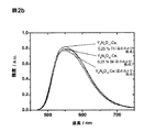
他の驚異的な効果は、本発明の蛍光体が、固体拡散法によって調製される同時ドープでないYAG:Ce蛍光体より高い光度を有することにある(図1および2を参照)。 Another surprising effect is that the phosphors of the present invention have a higher luminous intensity than non-codoped YAG: Ce phosphors prepared by solid state diffusion (see FIGS. 1 and 2).
したがって、本発明は、式I
(Ya,Gdb,Luc,Sed,Sme,Tbf,Prg,Thh,Iri,Sbj,Bik)3−x(All,Gam)5O12:Cex (I)
式中、
a+b+c+d+e+f+g+h+i+j+k=1であり、
l+m=1であり、
x=0.005〜0.1である、
で表されるガーネット構造を有する蛍光体に関する。
Accordingly, the present invention provides compounds of formula I
(Y a, Gd b, Lu c, Se d, Sm e, Tb f, Pr g, Th h, Ir i, Sb j, Bi k) 3-x (Al l, Ga m) 5 O 12: Ce x (I)
Where
a + b + c + d + e + f + g + h + i + j + k = 1,
l + m = 1,
x = 0.005 to 0.1.
It is related with the fluorescent substance which has the garnet structure represented by these.
本明細書中のガーネット構造はまた、この結晶が典型的なガーネット構造を保持する限り、必然的に、ガーネットの理想的な場合とわずかに異なる欠陥または格子の欠陥に基づく構造を意味する。典型的なガーネット構造は、一般的に、A3B5O12:Dを意味するものと解釈され、ここでA=希土類金属(RE);B=Al、Ga;およびD=REと置き換えられる活性剤、例えばセリウムである。 The garnet structure herein also means a structure based on defects or lattice defects that are slightly different from the ideal case of garnet, as long as the crystal retains a typical garnet structure. A typical garnet structure is generally taken to mean A 3 B 5 O 12 : D, where A = rare earth metal (RE); B = Al, Ga; and D = RE. An activator, for example cerium.
セリウムのドーピング濃度が0.5〜10重量%であるのが、好ましい。これは、特に好ましくは2.0〜5.0重量%、最も好ましくは3.0〜3.5重量%である。3.0〜3.5%のセリウム濃度にて、蛍光体の増大した吸収およびしたがって増大した光収率または一層大きい輝度が、一般的に発生する。一層高いセリウム濃度では、量子収量が減少し、したがって次に低下した光収率がもたらされる。 It is preferable that the doping concentration of cerium is 0.5 to 10% by weight. This is particularly preferably 2.0 to 5.0% by weight, most preferably 3.0 to 3.5% by weight. At concentrations of 3.0-3.5% cerium, increased absorption of the phosphor and thus increased light yield or greater brightness generally occurs. At higher cerium concentrations, the quantum yield is reduced, thus leading to a reduced light yield.
式Iで表されるルミネッセント材料の吸収および発光スペクトル、熱消失挙動および減衰期間τ1/eは、3価のカチオンの正確な組成に高度に依存する。上述の分光学的特性についての重要な要因は、Ce3+の12面体位置の結晶場強度またはCe−O結合の共有結合特徴、即ち酸素アニオンの有効負電荷およびアニオンと金属電子軌道との重複である。 The absorption and emission spectra, heat dissipation behavior and decay period τ 1 / e of the luminescent material of formula I are highly dependent on the exact composition of the trivalent cation. An important factor for the spectroscopic properties described above is the crystal field strength of the Ce 3+ dodecahedron position or the covalent nature of the Ce—O bond, ie the effective negative charge of the oxygen anion and the overlap between the anion and the metal electron orbital. is there.
一般的に、Ce3+発光帯([Xe]5d1→[Xe]4f1遷移)が、増大する結晶場強度を伴って、または増大する共有結合特性を伴って赤色スペクトル領域に移動することを、観察することができる。したがって、上記の式Iで表される組成または電子が豊富である(「容易に酸化可能な」)三価カチオンでのドーピングの結果、この方向において影響されるスペクトル特性がもたらされる。 In general, the Ce 3+ emission band ([Xe] 5d 1 → [Xe] 4f 1 transition) moves to the red spectral region with increasing crystal field strength or with increasing covalent properties. Can be observed. Thus, doping with a trivalent cation that is rich in composition or electrons ("easily oxidizable") as described above in Formula I results in spectral characteristics that are affected in this direction.
特に好ましいのは、式Iで表される蛍光体であり、ここで、式Iで表される化合物は、式II〜IVで表される化合物から選択される化合物である:
(Y1−x−yCexSby)3Al5O12、式中0.005≦x≦0.1および0.001≦y≦0.005 (II)
(Y1−x−yCexBiy)3Al5O12、式中0.005≦x≦0.1および0.001≦y≦0.005 (III)
(Y1−x−yCexThy)3Al5O12、式中0.005≦x≦0.1および0.001≦y≦0.005 (IV)
Particularly preferred are phosphors of the formula I, wherein the compound of the formula I is a compound selected from the compounds of the formulas II to IV:
(Y 1-x-y Ce x Sb y) 3 Al 5
(Y 1-xy Ce x Bi y ) 3 Al 5 O 12 , wherein 0.005 ≦ x ≦ 0.1 and 0.001 ≦ y ≦ 0.005 (III)
(Y 1-xy Ce x Th y ) 3 Al 5 O 12 , where 0.005 ≦ x ≦ 0.1 and 0.001 ≦ y ≦ 0.005 (IV)
ガーネット構造における構成成分Bi、SbまたはThの1種または2種以上の比率の増大により、本発明の蛍光体の発光波長が赤色方向に移動する。これは、暖かい白色光を発生させるために特に重要である。高い色再生を有する快適な光を発生させるために、異なる蛍光体、即ち緑色方向に移動した蛍光体、例えばY3(Al,Ga)5O12などと、本発明の蛍光体と、赤色蛍光体(例えば高いルーメン当量に寄与することができる赤色バンドまたは線エミッタ、例えばユウロピウムをドープしたタングステン酸塩、モリブデン酸塩および/またはリン酸塩)との混合物を用いるのが、有利である。さらに、青緑色蛍光体、例えばLu3Al5O12:Ce(LUAG:Ce)を混合することも、可能である。これにより、日光のVIS昼光スペクトルに極めて類似するほぼ連続的な発光スペクトルが得られる。 The emission wavelength of the phosphor of the present invention moves in the red direction by increasing the ratio of one or more of the constituent components Bi, Sb or Th in the garnet structure. This is particularly important for generating warm white light. In order to generate comfortable light having high color reproduction, different phosphors, that is, phosphors moved in the green direction, such as Y 3 (Al, Ga) 5 O 12 , the phosphor of the present invention, and red fluorescence It is advantageous to use a mixture with the body (for example a red band or line emitter that can contribute to a high lumen equivalent, for example europium doped tungstate, molybdate and / or phosphate). Furthermore, it is also possible to mix a blue-green phosphor, for example, Lu 3 Al 5 O 12 : Ce (LUAG: Ce). This gives a nearly continuous emission spectrum very similar to the VIS daylight spectrum of sunlight.
本発明の蛍光体の粒子の大きさは、50nm〜30μm、好ましくは1μm〜20μmである。 The particle size of the phosphor of the present invention is 50 nm to 30 μm, preferably 1 μm to 20 μm.
他の態様において、式Iで表される蛍光体は、さらに以下の蛍光体材料のさらなる少なくとも1種を含んでいてもよい:
酸化物、モリブデン酸塩、タングステン酸塩、バナジウム酸塩、III族窒化物、(オキシ)窒化物、各々個々に、または1種もしくは2種以上の活性剤イオン、例えばCe、Eu、Mn、Crおよび/またはBiとのこれらの混合物。
特定の色空間が確立されるべきである場合には、これは特に有利である。
In other embodiments, the phosphor of formula I may further comprise at least one further of the following phosphor materials:
Oxides, molybdates, tungstates, vanadates, group III nitrides, (oxy) nitrides, individually or one or more activator ions such as Ce, Eu, Mn, Cr And / or mixtures thereof with Bi.
This is particularly advantageous if a specific color space is to be established.
さらに好ましい態様において、蛍光体はLEDチップの反対側に、構造化された(例えばピラミッド状の)表面を有する(DE 102006054330.0、Merckを参照、これを、参照によりこの全範囲において本出願の文脈中に包含する)。これにより、可能な限り多量の光を蛍光体から結合させることが可能になる。 In a further preferred embodiment, the phosphor has a structured (eg pyramidal) surface on the opposite side of the LED chip (see DE 102006054330.0, Merck, which is hereby incorporated by reference in its entirety in the context of the present application). Included). This makes it possible to couple as much light as possible from the phosphor.
蛍光体の構造化された表面を、すでに構造化された好適な材料でその後コーティングすることにより、またはその後の段階において(フォト)リソグラフィープロセス、エッチングプロセスにより、あるいはエネルギーもしくは材料ビーム、または機械力の作用を用いた書き込みプロセスにより作製する。 By subsequently coating the structured surface of the phosphor with a suitable material already structured, or at a later stage by a (photo) lithographic process, an etching process, or by an energy or material beam, or mechanical force It is manufactured by a writing process using an action.
さらに好ましい態様において、本発明の蛍光体は、LEDチップの反対側に、SiO2、TiO2、Al2O3、ZnO2、ZrO2および/またはY2O3もしくはこれらの材料の組み合わせのナノ粒子または蛍光体組成物を含む粒子を担持する粗面を有する。粗面はここで、数百nmまでの粗さを有する。被覆した表面は、全反射を低減するかまたは防止することができ、光が本発明の蛍光体から一層良好に結合することができる(DE 102006054330.0 (Merck)を参照。これを、参照によりこの全範囲において本出願の文脈中に包含する)という利点を有する。 In a further preferred embodiment, the phosphor of the present invention is provided on the opposite side of the LED chip with nano-sized SiO 2 , TiO 2 , Al 2 O 3 , ZnO 2 , ZrO 2 and / or Y 2 O 3 or a combination of these materials. It has a rough surface carrying particles or particles containing a phosphor composition. The rough surface here has a roughness of up to several hundred nm. The coated surface can reduce or prevent total reflection and light can be better coupled from the phosphors of the invention (see DE 102006054330.0 (Merck), which is referred to by reference to this total). In the context of the present application in scope).
本発明の蛍光体がチップに面していない表面上に屈折率適合層を有し、これにより一次放射および/または蛍光体素子により発せられた放射の結合を単純化するのが、さらに好ましい。 It is further preferred that the phosphor of the present invention has a refractive index matching layer on the surface not facing the chip, thereby simplifying the coupling of the primary radiation and / or the radiation emitted by the phosphor element.
他の好ましい態様において、蛍光体は、SiO2、TiO2、Al2O3、ZnO、ZrO2および/またはY2O3またはこれらの混合物からなる連続的表面コーティングを有する。この表面コーティングは、屈折率を環境に適合させることを、コーティング材料の屈折率の好適な勾配により達成することができるという利点を有する。この場合において、蛍光体の表面における光の散乱は低減され、一層大きい比率の光は、蛍光体中に浸透し、吸収され、ここで変換され得る。加えて、全反射が低減されるため、屈折率適合される表面コーティングにより、一層多量の光が蛍光体から結合するのが可能になる。
In another preferred embodiment, the phosphor has a continuous surface coating of SiO 2, TiO 2, Al 2
加えて、蛍光体がカプセル封入されなければならない場合には、連続層は有利である。これは、直接的な周辺で水または他の物質を拡散させることに対する蛍光体またはこの一部の感受性に対処するために必要であり得る。連続さやでカプセル封入することについての他の理由は、チップにおいて発生する熱からの実際の蛍光体の熱分断である。この熱の結果、蛍光体の蛍光光収率が減少し、また蛍光の色に影響し得る。最後に、このタイプのコーティングにより、蛍光体の効率を、蛍光体中で発生する格子の振動が環境中に伝播するのを防止することにより上昇させるのが可能になる。 In addition, a continuous layer is advantageous when the phosphor has to be encapsulated. This may be necessary to address the sensitivity of the phosphor or part thereof to diffusing water or other materials in the immediate vicinity. Another reason for encapsulating with a continuous sheath is the thermal decoupling of the actual phosphor from the heat generated in the chip. As a result of this heat, the fluorescent light yield of the phosphor is reduced and can affect the color of the fluorescence. Finally, this type of coating makes it possible to increase the efficiency of the phosphor by preventing propagation of lattice vibrations that occur in the phosphor into the environment.
加えて、蛍光体が、SiO2、TiO2、Al2O3、ZnO、ZrO2および/またはY2O3またはこれらの混合酸化物または蛍光体組成物からなる多孔性表面コーティングを有するのが、好ましい。これらの多孔性コーティングは、単一の層の屈折率をさらに減少させる可能性を提供する。WO 03/027015に記載されているように、このタイプの多孔性コーティングを、3つの従来の方法により製造することができ、これを、参照によりこの全範囲において本出願の文脈中に包含する:ガラス(例えばソーダ石灰ガラス(US 4019884を参照))のエッチング、多孔質層の適用および多孔質層とエッチングプロセスとの組み合わせ。
In addition, phosphor, SiO 2, TiO 2, Al 2
他の好ましい態様において、蛍光体は、好ましくはエポキシまたはシリコーン樹脂からなる、周囲との化学結合を促進する官能基を担持する表面を有する。これらの官能基は、例えばオキソ基を介して結合しており、エポキシドおよび/またはシリコーンをベースとする結合剤の構成成分への結合を形成することができるエステル類または他の誘導体であり得る。このタイプの表面は、蛍光体を結合剤中に均質に混合することが容易になるという利点を有する。さらに、蛍光体/結合剤系およびまたポット寿命のレオロジー的特性を、したがってある程度調節することができる。したがって、混合物の加工は単純化される。 In another preferred embodiment, the phosphor has a surface bearing functional groups that facilitate chemical bonding with the surroundings, preferably made of epoxy or silicone resin. These functional groups are linked via, for example, oxo groups and can be esters or other derivatives that can form bonds to the components of epoxide and / or silicone based binders. This type of surface has the advantage that it facilitates the homogeneous mixing of the phosphor into the binder. Furthermore, the rheological properties of the phosphor / binder system and also the pot life can thus be adjusted to some extent. Thus, the processing of the mixture is simplified.
LEDチップに適用される本発明の蛍光体層が、好ましくはシリコーンと均一な蛍光体粒子との混合物からなり、シリコーンが表面張力を有するため、この蛍光体層は微視的なレベルにおいて不均一であるか、または層の厚さは完全に一定ではない。 The phosphor layer of the present invention applied to the LED chip is preferably composed of a mixture of silicone and uniform phosphor particles, and since the silicone has surface tension, the phosphor layer is non-uniform at a microscopic level. Or the layer thickness is not completely constant.
本発明はさらに、アルミニウム、イットリウムおよびセリウム含有出発物質を少なくとも1種のアンチモン、ビスマス、イリジウムおよび/またはトリウム含有同時ドーパント(co-dopant)と、任意にさらにガドリニウム、ルテニウム、セレン、サマリウム、テルビウム、プラセオジムおよび/またはガリウム含有物質と、湿式化学的方法により混合し、その後熱後処理することにより得られる、ガーネット構造を有する蛍光体に関する。 The present invention further provides aluminum, yttrium and cerium containing starting materials with at least one antimony, bismuth, iridium and / or thorium containing co-dopant and optionally further gadolinium, ruthenium, selenium, samarium, terbium, The present invention relates to a phosphor having a garnet structure, which is obtained by mixing with praseodymium and / or a gallium-containing substance by a wet chemical method and then performing a thermal post-treatment.
蛍光体を調製するための出発物質は、前述のように、ベース物質(例えばアルミニウム、イットリウムおよびセリウムの塩溶液)ならびに少なくとも1種のSb、Bi、IrまたはTh含有ドーパントならびに任意にさらにGd、Lu、Sc、Sm、Tb、Prおよび/またはGa含有物質からなる。好適な出発物質は、無機および/または有機物質、例えば金属、半金属、遷移金属および/または希土類元素の硝酸塩、炭酸塩、炭酸水素塩、リン酸塩、カルボン酸塩、アルコラート、酢酸塩、シュウ酸塩、ハロゲン化物、硫酸塩、有機金属化合物、水酸化物および/または酸化物であり、これを無機および/または有機液体中に溶解および/または懸濁させる。好ましいのは、対応する要素を所要の化学量論比で含む混合硝酸塩溶液、塩化物または水酸化物溶液を用いることである。 Starting materials for preparing the phosphors, as described above, include base materials (eg, aluminum, yttrium and cerium salt solutions) and at least one Sb, Bi, Ir or Th containing dopant and optionally further Gd, Lu , Sc, Sm, Tb, Pr and / or Ga-containing material. Suitable starting materials are inorganic and / or organic substances such as nitrates, carbonates, bicarbonates, phosphates, carboxylates, alcoholates, acetates, oxalates of metals, metalloids, transition metals and / or rare earth elements. Acid salts, halides, sulfates, organometallic compounds, hydroxides and / or oxides, which are dissolved and / or suspended in inorganic and / or organic liquids. Preference is given to using a mixed nitrate solution, chloride or hydroxide solution containing the corresponding elements in the required stoichiometric ratio.
本発明はさらに、以下のプロセス段階:
a)Sb、Biおよび/またはTh含有物質で同時ドープされたセリウムで活性化された蛍光体を、蛍光体前駆体懸濁液または溶液から、Y、Al、Ce、Gd、Lu、Sc、Sm、Tb、Prおよび/またはGa含有物質から選択される少なくとも3種の出発物質を湿式化学的方法により混合することにより調製すること、
b)Sb、Biおよび/またはThで同時ドープされた蛍光体を熱後処理すること
を有する蛍光体の製造方法に関する。
The present invention further comprises the following process steps:
a) A cerium-activated phosphor co-doped with Sb, Bi and / or Th-containing materials from a phosphor precursor suspension or solution, Y, Al, Ce, Gd, Lu, Sc, Sm Preparing by mixing at least three starting materials selected from Tb, Pr and / or Ga containing materials by wet chemical methods;
b) relates to a method for producing a phosphor comprising thermal post-treatment of a phosphor co-doped with Sb, Bi and / or Th.
湿式化学的調製は、一般的に、得られる材料が、本発明の蛍光体を調製する粒子の化学量論的組成、粒子の大きさおよび形態に関して一層大きい均一性を有するという、従来の固体拡散法にまさる利点を有する。 Wet chemical preparation generally involves a conventional solid state diffusion in which the resulting material has greater uniformity with respect to the stoichiometric composition, particle size and morphology of the particles from which the phosphors of the present invention are prepared. It has advantages over the law.
例えば硝酸イットリウム、硝酸アルミニウム、硝酸セリウムおよび硝酸ビスマス溶液の混合物からなる蛍光体の水性前駆体(蛍光体前駆体)の湿式化学的前処理のために、以下の既知の方法が好ましい: For example, the following known methods are preferred for wet chemical pretreatment of phosphor aqueous precursors (phosphor precursors) consisting of a mixture of yttrium nitrate, aluminum nitrate, cerium nitrate and bismuth nitrate solutions:
・NH4HCO3溶液での共沈(例えばJander, Blasius Lehrbuch der analyt. u. praep. anorg. Chem. [Textbook of Analyt. and Prep. Inorg. Chem.] 2002を参照)
・クエン酸およびエチレングリコールの溶液を用いるPecchini法(例えばAnnual Review of Materials Research Vol. 36: 2006, 281-331を参照)
・尿素を用いる燃焼法
・水溶液または有機塩溶液(出発物質)の噴霧乾燥
・水溶液または有機塩溶液(出発物質)の噴霧熱分解
・硝酸塩溶液の蒸発および残留物の熱変換
Co-precipitation with NH 4 HCO 3 solution (see, for example, Jander, Blasius Lehrbuch der analyt. U. Praep. Anorg. Chem. [Textbook of Analyt. And Prep. Inorg. Chem.] 2002)
Pecchini method using a solution of citric acid and ethylene glycol (see, for example, Annual Review of Materials Research Vol. 36: 2006, 281-331)
-Combustion method using urea-Spray drying of aqueous solution or organic salt solution (starting material)-Spray pyrolysis of aqueous solution or organic salt solution (starting material)-Evaporation of nitrate solution and thermal conversion of residue
前述の共沈において、NH4HCO3溶液を、例えば対応する蛍光体出発物質の硝酸塩溶液に加え、蛍光体前駆体の生成をもたらす。 In the aforementioned coprecipitation, NH 4 HCO 3 solution is added, for example, to the nitrate solution of the corresponding phosphor starting material, resulting in the production of phosphor precursors.
Pecchini法において、クエン酸およびエチレングリコールからなる沈殿試薬を、例えば対応する蛍光体出発物質の前述の硝酸塩溶液に、室温にて加え、混合物をその後加熱する。粘性が上昇する結果、蛍光体前駆体が生成する。 In the Pecchini method, a precipitation reagent consisting of citric acid and ethylene glycol is added, for example, to the aforementioned nitrate solution of the corresponding phosphor starting material at room temperature and the mixture is then heated. As a result of the increased viscosity, a phosphor precursor is generated.
既知の燃焼方法において、対応する蛍光体出発物質の前述の硝酸塩溶液を、例えば水に溶解し、次に還流下で沸騰させ、尿素で処理し、この結果、蛍光体前駆体がゆっくりと生成する。 In known combustion methods, the aforementioned nitrate solution of the corresponding phosphor starting material is dissolved, for example in water, then boiled under reflux and treated with urea, resulting in the slow production of phosphor precursors. .
噴霧熱分解は、エアゾール方法の1つであり、これは、種々の方法で加熱した反応空間(反応器)中に溶液、懸濁液または分散体を噴霧し、固体粒子を形成し、沈殿させることにより特徴づけられる。<200℃の高温ガス温度を用いる噴霧乾燥とは対照的に、高温プロセスとしてのスプレー熱分解において、溶媒の蒸発に加えて、用いる出発物質(たとえば塩類)の熱分解および物質(例えば酸化物、混合酸化物)の再生成がさらに発生する。 Spray pyrolysis is an aerosol method that sprays solutions, suspensions or dispersions into reaction spaces (reactors) heated in various ways to form and precipitate solid particles. It is characterized by that. In contrast to spray drying using a hot gas temperature of <200 ° C., in spray pyrolysis as a high temperature process, in addition to solvent evaporation, pyrolysis of the starting materials used (eg salts) and materials (eg oxides, Further regeneration of the mixed oxide) occurs.
前述の6つの方法の変法は、DE 102006027133.5 (Merck)中に詳細に記載されており、これを、参照によりこの全範囲において本出願の文脈中に包含する。 Variations of the foregoing six methods are described in detail in DE 102006027133.5 (Merck), which is incorporated in the context of the present application in its entirety by reference.
本発明の蛍光体を、以下による種々の湿式化学的方法により調製することができる。
1)構成成分を均一に沈殿させ、次に溶媒を分離し、続いて単一段階の、または多段階の熱後処理を施し、ここでこれらの段階の1つを還元雰囲気中で行ってもよい、
2)例えば噴霧プロセスの補助により、混合物を微細に分割し、溶媒を除去し、続いて単一段階の、または多段階の熱後処理を施し、ここでこれらの段階の1つを還元雰囲気中で行ってもよい、あるいは、
The phosphor of the present invention can be prepared by various wet chemical methods as follows.
1) Precipitating the constituents homogeneously, then separating the solvent, followed by a single-stage or multi-stage thermal post-treatment, where one of these stages may be carried out in a reducing atmosphere Good,
2) The mixture is finely divided, for example with the aid of a spraying process, the solvent is removed, followed by a single-stage or multi-stage heat treatment, where one of these stages is carried out in a reducing atmosphere Or you can go
3)例えば噴霧プロセスの補助により、混合物を微細に分割し、溶媒を熱分解との関連において除去し、続いて単一段階の、または多段階の熱後処理を施し、ここでこれらの段階の1つを還元雰囲気中で行ってもよい、
4)その後、方法1〜3の補助により調製した蛍光体をコーティングして、これらの環境への屈折率適合を達成する。
3) The mixture is finely divided, for example with the aid of a spraying process, the solvent is removed in the context of pyrolysis, followed by a single-stage or multi-stage heat treatment, where One may be performed in a reducing atmosphere,
4) The phosphor prepared with the aid of methods 1-3 is then coated to achieve refractive index matching to these environments.
蛍光体の湿式化学的調製を、好ましくは沈殿および/またはゾル−ゲル法により行う。
前述の熱後処理において、か焼を、還元条件(例えば一酸化炭素、フォーミングガス、純粋な水素または少なくとも真空であるかもしくは酸素欠乏雰囲気を用いる)下で少なくとも部分的に行うのが、好ましい。
The wet chemical preparation of the phosphor is preferably carried out by precipitation and / or sol-gel methods.
In the aforementioned thermal aftertreatment, calcination is preferably carried out at least partly under reducing conditions (eg using carbon monoxide, forming gas, pure hydrogen or at least a vacuum or using an oxygen-deficient atmosphere).
一般的に、固体拡散方法によって本発明の蛍光体を調製することも可能であるが、これは、すでに述べた欠点を生じる。
前述の方法により、蛍光体粒子のすべての所望の外形、例えば球状粒子、薄片または構造化された材料およびセラミックスを作製するのが可能になる。
In general, it is also possible to prepare the phosphors of the invention by a solid diffusion method, but this results in the disadvantages already mentioned.
The method described above makes it possible to produce all desired contours of phosphor particles, such as spherical particles, flakes or structured materials and ceramics.
他の好ましい態様として、薄片形態の蛍光体を、対応する金属および/または希土類元素塩から従来の方法により調製する。調製方法は、EP 763573およびDE 102006054331.9に詳細に記載されており、これらを、参照によりこれらの全範囲において本出願の文脈中に包含する。これらの薄片形態の蛍光体を、極めて大きいアスペクト比、原子的に平滑な表面および調整可能な厚さを有する、例えばマイカ薄片、SiO2薄片、Al2O3薄片、ZrO2薄片、ガラス薄片またはTiO2薄片製の、天然の、または合成的に製造された高度に安定な支持体または基板を、蛍光体層で、水性分散体または懸濁液中で沈殿反応によりコーティングすることによって、調製することができる。 In another preferred embodiment, the flake form phosphor is prepared from the corresponding metal and / or rare earth element salt by conventional methods. Preparation methods are described in detail in EP 763573 and DE 102006054331.9, which are incorporated in the context of the present application in their entire scope by reference. These flake-form phosphors have a very high aspect ratio, atomically smooth surface and adjustable thickness, for example mica flakes, SiO 2 flakes, Al 2 O 3 flakes, ZrO 2 flakes, glass flakes or A TiO 2 flake, natural or synthetically produced highly stable support or substrate is prepared by coating with a phosphor layer, in an aqueous dispersion or suspension, by a precipitation reaction. be able to.
マイカ、ZrO2、SiO2、Al2O3、ガラスもしくはTiO2またはこれらの混合物以外に、薄片はまた、蛍光体材自体からなるか、または材料から構築されていてもよい。薄片自体が単に蛍光体コーティングについての支持体として供されるに過ぎない場合には、後者は、LEDからの一次放射に対して透明であるか、または一次放射を吸収し、このエネルギーを蛍光体層に伝達する材料からならなければならない。薄片形態の蛍光体を、樹脂(例えばシリコーンまたはエポキシ樹脂)中に分散させ、この分散体を、LEDチップに適用する。 Besides mica, ZrO 2 , SiO 2 , Al 2 O 3 , glass or TiO 2 or mixtures thereof, the flakes may also consist of the phosphor material itself or be constructed from materials. If the flakes themselves merely serve as a support for the phosphor coating, the latter is transparent to the primary radiation from the LED or absorbs the primary radiation and this energy is transferred to the phosphor. Must be made of material that transmits to the layer. The phosphor in the form of flakes is dispersed in a resin (for example, silicone or epoxy resin), and this dispersion is applied to the LED chip.
薄片形態の蛍光体を、50nm〜約20μm、好ましくは150nm〜5μmの厚さで、工業的大規模で調製することができる。ここでの直径は、50nm〜20μmである。
これは、一般的に、1:1〜400:1、特に3:1〜100:1のアスペクト比(直径対粒子の厚さの比率)を有する。
薄片の大きさ(長さ×幅)は、配置に依存する。薄片はまた、特にこれらが特に小さい寸法を有する場合には、変換層内の散乱の中心部としても適する。
Flake-form phosphors can be prepared on a large industrial scale with a thickness of 50 nm to about 20 μm, preferably 150 nm to 5 μm. The diameter here is 50 nm to 20 μm.
This generally has an aspect ratio (diameter to particle thickness ratio) of 1: 1 to 400: 1, in particular 3: 1 to 100: 1.
The size of the flakes (length x width) depends on the arrangement. The flakes are also suitable as the center of scattering in the conversion layer, especially if they have particularly small dimensions.
LEDチップに面する本発明の薄片形態の蛍光体の表面は、LEDチップにより発せられた一次放射に関する反射低減作用を有するコーティングを備えることができる。この結果、一次放射の後方散乱の低減がもたらされ、後者の本発明の蛍光体素子中への結合が増強される。 The surface of the flake-form phosphor of the present invention facing the LED chip can be provided with a coating having a reflection reducing effect on the primary radiation emitted by the LED chip. This results in a reduction in the backscattering of the primary radiation and enhances the latter coupling into the inventive phosphor element.
この目的のために適するのは、例えば、以下の厚さd:d=[LEDチップからの一次放射の波長/(4×蛍光体セラミックスの屈折率)]を有しなければならない、屈折率適合されたコーティングである。例えば、Gerthsen, Physik [Physics], Springer Verlag, 第18版、1995を参照。このコーティングはまた、フォトニック結晶からなっていてもよく、これはまた、特定の機能を達成するために薄片形態の蛍光体の表面を構造化することを包含する。 Suitable for this purpose is, for example, the following thickness d: d = [wavelength of primary radiation from the LED chip / (4 × refractive index of the phosphor ceramic)], refractive index adaptation Coating. See, for example, Gerthsen, Physik [Physics], Springer Verlag, 18th edition, 1995. This coating may also consist of a photonic crystal, which also includes structuring the surface of the phosphor in the form of flakes to achieve a specific function.
セラミックス素子の形態の本発明の蛍光体の調製を、DE 102006037730 (Merck)に記載されている方法と同様に行い、これを、参照によりこの全範囲において本出願の文脈中に包含する。蛍光体をここで、対応する出発物質とドーパントとを湿式化学的方法により混合し、その後混合物を平衡に加圧し、均一であり、薄い、無孔の薄片の形態のチップの表面に混合物を直接適用することにより、調製する。蛍光体の励起および放出の位置に依存する変化はこのように発生せず、これと共に提供されるLEDを生じて、恒常的な色の均一な光錐を発し、高い発光力(luminous power)を有する。 The preparation of the phosphors according to the invention in the form of ceramic elements is carried out analogously to the method described in DE 102006037730 (Merck), which is hereby incorporated in the context of the present application in its entirety. The phosphor is now mixed with the corresponding starting materials and dopants by wet chemical methods, after which the mixture is pressed to equilibrium, and the mixture is applied directly to the surface of the chip in the form of a uniform, thin, non-porous flake. Prepare by applying. No change depending on the position of excitation and emission of the phosphor occurs in this way, resulting in an LED provided with it, emitting a uniform light cone of constant color and high luminous power. Have.
セラミックス蛍光体素子を、工業的大規模で、例えば数百nm〜約500μmの厚さの薄片として、製造することができる。薄片の大きさ(長さ×幅)は、配置に依存する。チップに直接適用する場合において、薄片の寸法を、好適なチップ配置の場合(例えばフリップチップ配置)において、または、対応して、約10%〜30%のチップ表面の特定の過剰な大きさでチップの大きさ(約100μm×100μmないし数mm2)に従って選択しなければならない。蛍光体薄片を完成したLEDの最上部に装着する場合には、発せられた光錐はすべて、薄片に達する。 The ceramic phosphor element can be manufactured on a large industrial scale, for example, as a flake having a thickness of several hundred nm to about 500 μm. The size of the flakes (length x width) depends on the arrangement. In the case of direct application to the chip, the dimensions of the flakes are in the case of a suitable chip arrangement (e.g. flip chip arrangement) or correspondingly with a certain excess size of the chip surface of about 10% to 30%. Selection should be made according to the size of the chip (approximately 100 μm × 100 μm to several mm 2 ). When the phosphor flakes are mounted on top of the completed LED, all emitted light cones reach the flakes.
セラミックス蛍光体素子の側面を、軽金属または貴金属、好ましくはアルミニウムまたは銀で金属化することができる。金属化は、光が蛍光体要素から側方に進出しないという効果を有する。側方に進出する光は、LEDから結合する光束を低減し得る。セラミックス蛍光体素子の金属化を、平衡加圧の後のプロセス段階において行って、棒または薄片を得、ここで、所望により、棒または薄片を、金属化の前に所要の大きさに切断することができる。このために、側面を、例えば硝酸銀およびグルコースの溶液で湿潤させ、その後上昇した温度にてアンモニア雰囲気に曝露する。この操作の間、銀コーティングが、例えば側面上に形成する。 The side surface of the ceramic phosphor element can be metallized with a light metal or a noble metal, preferably aluminum or silver. Metallization has the effect that light does not advance laterally from the phosphor element. The light that advances to the side can reduce the luminous flux combined from the LED. Metallization of the ceramic phosphor element is performed in a process step after equilibrium pressing to obtain a bar or flake, where the bar or flake is optionally cut to the required size prior to metallization. be able to. For this, the sides are wetted with, for example, a solution of silver nitrate and glucose and then exposed to an ammonia atmosphere at an elevated temperature. During this operation, a silver coating forms, for example on the side.
あるいはまた、無電解金属化方法が、好適である。例えば、Hollemann-Wiberg, Lehrbuch der anorganischen Chemie [Textbook of Inorganic Chemistry], Walter de Gruyter VerlagまたはUllmanns Enzyklopaedie der chemischen Technologie [Ullmann's Encyclopaedia of Chemical Technology]を参照。
セラミックス蛍光体素子を、所要に応じて、水ガラス溶液を用いてLEDチップの基板に固定することができる。
Alternatively, an electroless metallization method is suitable. See, for example, Hollemann-Wiberg, Lehrbuch der anorganischen Chemie [Textbook of Inorganic Chemistry], Walter de Gruyter Verlag or Ullmanns Enzyklopaedie der chemischen Technologie [Ullmann's Encyclopaedia of Chemical Technology].
The ceramic phosphor element can be fixed to the substrate of the LED chip using a water glass solution as required.
他の態様において、セラミックス蛍光体素子は、LEDチップの反対側に構造化された(例えばピラミッド状の)表面を有する。これにより、可能な限り多量の光が蛍光体素子から結合するのが可能になる。蛍光体素子上の構造化された表面を、構造化されたプレスプレートを有し、したがって構造を表面にエンボス加工する型を用いた均衡な押圧を行うことにより作製する。目的が可能な限り薄い蛍光体素子または薄片を製造することにある場合には、構造化された表面が望ましい。押圧条件は、当業者に知られている(J. Kriegsmann, Technische keramische Werkstoffe [Industrial Ceramic Materials], 第4章、Deutscher Wirtschaftsdienst, 1998を参照)。用いる押圧温度が押圧される物質の融点の2/3〜5/6であることが、重要である。
In other embodiments, the ceramic phosphor element has a structured (eg, pyramidal) surface on the opposite side of the LED chip. This allows as much light as possible to couple from the phosphor element. The structured surface on the phosphor element is made by performing a balanced pressing using a mold having a structured press plate and thus embossing the structure on the surface. A structured surface is desirable when the goal is to produce as thin a phosphor element or flake as possible. The pressing conditions are known to those skilled in the art (see J. Kriegsmann, Technische keramische Werkstoffe [Industrial Ceramic Materials],
加えて、本発明の蛍光体を、約410nm〜530nm、好ましくは430nm〜約500nmに及ぶ広範囲にわたり、励起させることができる。したがって、これらの蛍光体は、UVまたは青色発光一次光源、例えばLED、または従来の放電ランプ(例えばHgをベースとする)による励起に適するのみならず、451nmにて青色In3+線を用いるものなどの光源にも適する。 In addition, the phosphors of the present invention can be excited over a wide range ranging from about 410 nm to 530 nm, preferably from 430 nm to about 500 nm. Therefore, these phosphors are not only suitable for excitation by UV or blue light emitting primary light sources such as LEDs or conventional discharge lamps (eg Hg based), but also those using blue In 3+ rays at 451 nm, etc. Suitable for light sources.
本発明はさらに、発光極大が410nm〜530nm、好ましくは430nm〜約500nm、特に好ましくは440〜480nmの範囲内にある少なくとも1つの一次光源を有する照明ユニットに関し、ここで一次放射は、本発明の蛍光体によってより長い波長の放射に部分的に、または完全に変換される。この照明ユニットは、好ましくは白色光を発光するか、または特定の色点(カラーオンデマンド原理)を有する光を発光する。本発明の照明単位の好ましい態様を、図3〜14に示す。 The invention further relates to an illumination unit having at least one primary light source whose emission maximum is in the range of 410 nm to 530 nm, preferably 430 nm to about 500 nm, particularly preferably 440 to 480 nm, wherein the primary radiation is It is partially or completely converted to longer wavelength radiation by the phosphor. This lighting unit preferably emits white light or emits light having a specific color point (color on demand principle). The preferable aspect of the illumination unit of this invention is shown to FIGS.
本発明の照明ユニットの好ましい態様において、光源は、ルミネッセンス性の窒化インジウムアルミニウムガリウム、特に式IniGajAlkNで表され、式中0≦i、0≦j、0≦k、およびi+j+k=1であるものである。照明ユニットは、好ましくは白色放射である。このタイプの光源の可能な形態は、当業者に知られている。これらは、種々の構造を有する発光LEDチップであり得る。 In a preferred embodiment of the lighting unit according to the invention, the light source is represented by a luminescent indium aluminum gallium nitride, in particular the formula In i Ga j Al k N, where 0 ≦ i, 0 ≦ j, 0 ≦ k, and i + j + k. = 1. The lighting unit is preferably white radiation. Possible forms of this type of light source are known to those skilled in the art. These can be light emitting LED chips having various structures.
本発明の照明ユニットの他の好ましい態様において、光源は、ZnO、TCO(透明伝導性酸化物)、ZnSeもしくはSiCをベースとするルミネッセンス配置または有機発光層(OLED)をベースとする配置である。 In another preferred embodiment of the lighting unit according to the invention, the light source is a luminescence arrangement based on ZnO, TCO (transparent conductive oxide), ZnSe or SiC or an arrangement based on an organic light emitting layer (OLED).
本発明の照明ユニットの他の好ましい態様において、光源は、エレクトロルミネッセンスおよび/またはフォトルミネッセンスを示す光源である。光源はさらにまた、プラズマまたは放電源であってもよい。 In another preferred embodiment of the lighting unit of the present invention, the light source is a light source exhibiting electroluminescence and / or photoluminescence. The light source may also be a plasma or a discharge source.
本発明の蛍光体を、樹脂(例えばエポキシもしくはシリコーン樹脂)中に分散させるか、または好適な大きさの比率の場合には、一次光源上に直接配置するかまたは、用途に依存して、これから遠隔に配置することができる(後者の配置はまた、「遠隔蛍光体技術(remote phosphor technology)」をも含む)。遠隔蛍光体技術の利点は、当業者に知られており、例えば以下の刊行物において明らかにされている: Japanese Journ. of Appl. Phys. 第44巻、No. 21 (2005), L649-L651。 The phosphors of the present invention are dispersed in a resin (eg, epoxy or silicone resin) or, if in a suitable size ratio, placed directly on the primary light source or depending on the application It can be remotely located (the latter arrangement also includes “remote phosphor technology”). The advantages of remote phosphor technology are known to those skilled in the art and are elucidated, for example, in the following publications: Japanese Journ. Of Appl. Phys. Vol. 44, No. 21 (2005), L649-L651 .
他の態様において、蛍光体と一次光源との間の照明ユニットの光学的結合が光伝導性の配置により達成されるのが、好ましい。これにより、一次光源が、中心の位置に設置され、光伝導性装置、例えば光伝導ファイバーにより蛍光体に光学的に結合されるのが可能になる。このようにして、照明の希望に整合し、単に1種、または種々の蛍光体からなり、光スクリーンおよび光伝導体を形成するように配置することができ、一次光源に結合するランプを、達成することができる。このようにして、さらなる電気的配線を伴わずに、代わりに単に光伝導体を配置することにより、強力な一次光源を、電気的設置に好ましい位置に位置させること、および光伝導体に結合される蛍光体を含むランプを、任意の所望の位置において設置することが、可能である。 In other embodiments, it is preferred that the optical coupling of the illumination unit between the phosphor and the primary light source is achieved by a photoconductive arrangement. This allows the primary light source to be placed at the center and optically coupled to the phosphor by a photoconductive device, such as a photoconductive fiber. In this way, a lamp is achieved that matches the wishes of the lighting and consists only of one or a variety of phosphors, which can be arranged to form a light screen and a photoconductor, coupled to the primary light source. can do. In this way, a powerful primary light source can be located in a preferred location for electrical installation and coupled to the photoconductor by simply placing the photoconductor instead of further electrical wiring. It is possible to install a lamp containing a fluorescent material at any desired location.
本発明はさらに、発光ダイオードからの青色または近UV発光を部分的に、または完全に変換するための、本発明の蛍光体の使用に関する。
本発明の蛍光体を、さらに、好ましくは、青色または近UV発光を可視白色放射に変換するために用いる。本発明の蛍光体を、さらに、好ましくは、「カラーオンデマンド」概念によって一次放射を特定の色点に変換するために用いる。
The invention further relates to the use of the phosphor according to the invention for partial or complete conversion of blue or near UV emission from light emitting diodes.
The phosphors of the present invention are further preferably used to convert blue or near UV emission into visible white radiation. The phosphors of the present invention are further preferably used to convert primary radiation to a specific color point by the “color on demand” concept.
本発明はさらに、本発明の蛍光体を、エレクトロルミネッセント材料、例えばエレクトロルミネッセントフィルム(また発光フィルムまたは光フィルムとしても知られている)において用いることに関し、ここで、例えば、硫化亜鉛またはMn2+、Cu+もしくはAg+がドープされている硫化亜鉛をエミッタとして用い、これは黄緑色領域において発光する。エレクトロルミネッセントフィルムの適用の領域は、例えば広告、液晶ディスプレイスクリーン(LCディスプレイ)におけるディスプレイ背面照射および薄膜トランジスタ(TFT)ディスプレイ、自己照射車両ナンバープレート、床面の図形(破砕耐性かつ滑り止め積層体と組み合わせて)、例えば自動車、列車、船舶および航空機におけるディスプレイおよび/または制御素子において、またはまた屋内電気器具、庭設備、測定機器またはスポーツおよびレジャー用の設備である。 The invention further relates to the use of the phosphors of the invention in electroluminescent materials, such as electroluminescent films (also known as light-emitting films or light films), where, for example, zinc sulfide Alternatively, zinc sulfide doped with Mn 2+ , Cu + or Ag + is used as an emitter, which emits light in the yellow-green region. Areas of application of electroluminescent films include, for example, advertising, backside illumination and thin film transistor (TFT) displays on liquid crystal display screens (LC displays), self-illuminated vehicle license plates, floor graphics (crush-resistant and non-slip laminates) In combination) with, for example, displays and / or control elements in cars, trains, ships and aircraft, or also indoor appliances, garden equipment, measuring equipment or sports and leisure equipment.
以下の例は、本発明を例示することを意図する。しかし、これらは、いかなる方法によっても限定的であると考慮するべきではない。組成物中で用いることができるすべての化合物または成分は、既知であり、商業的に入手できるか、または既知の方法により合成することができる。例中に示す温度は、常に℃で示す。さらに、明細書においても、また例においても共に、組成物中の成分の添加量は、常に合計100%に加えられることは、言うまでもない。示す百分率のデータは、常に所定の関連において考慮しなければならない。しかし、これらは通常、常に示す部分量の重量または合計量に関する。 The following examples are intended to illustrate the present invention. However, these should not be considered limiting in any way. All compounds or components that can be used in the composition are known, commercially available, or can be synthesized by known methods. The temperatures shown in the examples are always in ° C. Furthermore, it goes without saying that both in the specification and in the examples, the addition amount of the components in the composition is always added to 100% in total. The percentage data shown must always be considered in the given context. However, these usually relate to the weight or total amount of partial amounts always indicated.
例
例1:湿式化学的方法による蛍光体(Y0.939Ce0.06Th0.001)3Al5O12の調製
537.6gの炭酸水素アンモニウムを、3リットルの脱イオン水に溶解する。205.216gの塩化アルミニウム六水和物、151.522gの塩化イットリウム六水和物、3.617gの塩化セリウム六水和物および0.191gの塩化トリウム(IV)を、約400mlの脱イオン水に溶解し、炭酸水素溶液に迅速に滴加する。この添加の間、濃アンモニアを加えることにより、pHをpH 8に維持しなければならない。その後、混合物を、さらに1時間撹拌する。熟成させた後、沈殿物を濾別し、乾燥キャビネット中で約120℃にて乾燥する。
Example 1: Preparation of phosphor (Y 0.939 Ce 0.06 Th 0.001 ) 3 Al 5 O 12 by wet chemical method 537.6 g of ammonium bicarbonate is dissolved in 3 liters of deionized water. . 205.216 g of aluminum chloride hexahydrate, 151.522 g of yttrium chloride hexahydrate, 3.617 g of cerium chloride hexahydrate and 0.191 g of thorium (IV) chloride were added to about 400 ml of deionized water. And quickly added dropwise to the bicarbonate solution. During this addition, the pH must be maintained at
乾燥沈殿物を、乳鉢中で粉砕し、その後1000℃にて空気中で4時間か焼する。その後、生成物を、乳鉢中で再び粉砕し、1700℃にて水素/アルゴン雰囲気中で8時間か焼する。 The dried precipitate is ground in a mortar and then calcined in air at 1000 ° C. for 4 hours. The product is then ground again in a mortar and calcined at 1700 ° C. in a hydrogen / argon atmosphere for 8 hours.
例2:湿式化学的方法による蛍光体(Y0.939Ce0.06Bi0.001)3Al5O12の調製
537.6gの炭酸水素アンモニウムを、3リットルの脱イオン水に溶解する。205.216gの塩化アルミニウム六水和物、151.522gの塩化イットリウム六水和物、3.617gの塩化セリウム六水和物および0.161gの塩化ビスマス(III)を、約400mlの脱イオン水に溶解し、炭酸水素溶液に迅速に滴加する。この添加の間、濃アンモニアを加えることにより、pHをpH 8に維持しなければならない。その後、混合物を、さらに1時間撹拌する。熟成させた後、沈殿物を濾別し、乾燥キャビネット中で約120℃にて乾燥する。
Example 2: Preparation of phosphor by wet chemical method (Y 0.939 Ce 0.06 Bi 0.001 ) 3 Al 5 O 12 537.6 g of ammonium bicarbonate are dissolved in 3 liters of deionized water. 205.216 g of aluminum chloride hexahydrate, 151.522 g of yttrium chloride hexahydrate, 3.617 g of cerium chloride hexahydrate and 0.161 g of bismuth (III) chloride were added to about 400 ml of deionized water. And quickly added dropwise to the bicarbonate solution. During this addition, the pH must be maintained at
乾燥沈殿物を、乳鉢中で粉砕し、その後1000℃にて空気中で4時間か焼する。その後、生成物を、乳鉢中で再び粉砕し、1700℃にて水素/アルゴン雰囲気中で8時間か焼する。 The dried precipitate is ground in a mortar and then calcined in air at 1000 ° C. for 4 hours. The product is then ground again in a mortar and calcined at 1700 ° C. in a hydrogen / argon atmosphere for 8 hours.
例3:湿式化学的方法による蛍光体(Y0.939Ce0.06Sb0.001)3Al5O12の調製
537.6gの炭酸水素アンモニウムを、3リットルの脱イオン水に溶解する。205.216gの塩化アルミニウム六水和物、151.522gの塩化イットリウム六水和物、3.617gの塩化セリウム六水和物および0.116gの塩化アンチモン(III)を、約400mlの脱イオン水に溶解し、炭酸水素溶液に迅速に滴加する。この添加の間、濃アンモニアを加えることにより、pHをpH 8に維持しなければならない。その後、混合物を、さらに1時間撹拌する。熟成させた後、沈殿物を濾別し、乾燥キャビネット中で約120℃にて乾燥する。
Example 3: Preparation of phosphor by wet chemical method (Y 0.939 Ce 0.06 Sb 0.001 ) 3 Al 5 O 12 537.6 g of ammonium bicarbonate are dissolved in 3 liters of deionized water. 205.216 g of aluminum chloride hexahydrate, 151.522 g of yttrium chloride hexahydrate, 3.617 g of cerium chloride hexahydrate and 0.116 g of antimony (III) chloride were added to about 400 ml of deionized water. And quickly added dropwise to the bicarbonate solution. During this addition, the pH must be maintained at
乾燥沈殿物を、乳鉢中で粉砕し、その後1000℃にて空気中で4時間か焼する。その後、生成物を、乳鉢中で再び粉砕し、1700℃にて水素/アルゴン雰囲気中で8時間か焼する。 The dried precipitate is ground in a mortar and then calcined in air at 1000 ° C. for 4 hours. The product is then ground again in a mortar and calcined at 1700 ° C. in a hydrogen / argon atmosphere for 8 hours.
例4:混合および焼成法(固体拡散)によるYAG:Ce(Ceドーピング濃度は2%、Y2.94Al5O12:Ce0.06 3+)の調製
0.344gの二酸化セリウム(CeO2)、33.646gの酸化イットリウム(Y2O3)および25.491gの酸化アルミニウム(Al2O3)を秤量し、水でスラリーにする。この混合物を、乳鉢中で少量の水を用いることにより湿式粉砕する。次に、スラリーを、チャンバー炉中に移送し、ここでこれを、フォーミングガス雰囲気中で1200℃の温度にて6時間にわたりか焼する。冷却後、材料を再び微細に粉砕し、これに、炉中で1700℃の温度にて8時間にわたり、還元的か焼を施す。
Example 4: Preparation of YAG: Ce (
例5:湿式化学的方法によるYAG:Ce(Ceドーピング濃度は2%、Y2.94Al5O12:Ce0.06 3+)の調製
537.6gの炭酸水素アンモニウムを、3リットルの脱イオン水に溶解する。205.216gの塩化アルミニウム六水和物、153.242gの塩化イットリウム六水和物および3.617gの塩化セリウム六水和物を、約400mlの脱イオン水に溶解し、炭酸水素溶液に迅速に滴加する。この添加の間、濃アンモニアを加えることにより、pHをpH 8に維持しなければならない。その後、混合物を、さらに1時間撹拌する。熟成させた後、沈殿物を濾別し、乾燥キャビネット中で約120℃にて乾燥する。
Example 5: YAG by wet-chemical methods: Ce (Ce doping concentration 2%, Y 2.94 Al 5 O 12: Ce 0.06 3+) ammonium bicarbonate preparation 537.6g of 3 liters of deionized Dissolve in water. 205.216 g of aluminum chloride hexahydrate, 153.242 g of yttrium chloride hexahydrate and 3.617 g of cerium chloride hexahydrate are dissolved in about 400 ml of deionized water and rapidly dissolved in a bicarbonate solution. Add dropwise. During this addition, the pH must be maintained at
乾燥沈殿物を、乳鉢中で粉砕し、その後1000℃にて空気中で4時間か焼する。その後、生成物を、乳鉢中で再び粉砕し、1700℃にて水素/アルゴン雰囲気中で8時間か焼する。 The dried precipitate is ground in a mortar and then calcined in air at 1000 ° C. for 4 hours. The product is then ground again in a mortar and calcined at 1700 ° C. in a hydrogen / argon atmosphere for 8 hours.
例6〜8:混合および焼成法(固体拡散)による蛍光体(Y0.98−xCe0.02Thx)3Al5O12(式中x=0.001;x=0.0025およびx=0.005)の調製
12.5mmolのガンマ−酸化アルミニウムAl2O3、7.35mmol−xの酸化イットリウムY2O3、0.3mmolの二酸化セリウムCeO2および0.015mmol≦x≦0.075mmolの酸化トリウムThO2を、秤量する。その後、出発物質をアセトンでスラリーにし、乳鉢中で十分に粉砕する。最初のか焼段階において、試料を、1200℃にて一酸化炭素の下で2時間加熱する。乳鉢中でさらに十分に粉砕した後、第2のか焼段階を行い、ここで、バッチを、1650℃にて、同様に一酸化炭素雰囲気下で4時間加熱する。
Examples 6-8: Phosphor (Y 0.98-x Ce 0.02 Th x ) 3 Al 5 O 12 (where x = 0.001; x = 0. Preparation of x = 0.005) 12.5 mmol gamma-aluminum oxide Al 2 O 3 , 7.35 mmol-x yttrium oxide Y 2 O 3 , 0.3 mmol cerium dioxide CeO 2 and 0.015 mmol ≦ x ≦ 0 Weigh out 075 mmol of thorium oxide ThO 2 . The starting material is then slurried with acetone and ground thoroughly in a mortar. In the first calcination stage, the sample is heated at 1200 ° C. under carbon monoxide for 2 hours. After further pulverization in a mortar, a second calcination step is performed, where the batch is heated at 1650 ° C., also in a carbon monoxide atmosphere, for 4 hours.
乳鉢中で最終的に粉砕した後、試料を、X線粉末回折法、ルミネッセンス分光法および反射分光法により特徴づけする。 After final grinding in a mortar, the sample is characterized by X-ray powder diffractometry, luminescence spectroscopy and reflection spectroscopy.
本発明を、多数の実施例を参照して以下に一層詳細に説明し、ここで:
(x,y) CIE 1937色度図における色点:
(Y0.969Ce0.02X0.001)3Al5O12、
ここでX=Sb:(x/y)=0.438/0.541、
ここでX=Bi:(x/y)=0.440/0.539、
ここでX=Th:(x/y)=0.439/0.541
固体拡散反応により調製された商業的なYAG:Ce:
(x/y)=0.435/0.541
湿式化学的方法により調製されたYAG:Ce:
(x/y)=0.435/0.541
(X, y) Color points in the CIE 1937 chromaticity diagram:
(Y 0.969 Ce 0.02 X 0.001 ) 3 Al 5 O 12 ,
Where X = Sb: (x / y) = 0.438 / 0.541
Where X = Bi: (x / y) = 0.440 / 0.539,
Where X = Th: (x / y) = 0.439 / 0.541
Commercial YAG: Ce prepared by solid state diffusion reaction:
(X / y) = 0.435 / 0.541
YAG: Ce prepared by wet chemical method:
(X / y) = 0.435 / 0.541
発光は、本発明の蛍光体の層33により形成する被覆層によって、黄色の二次的に発せられた光に部分的に変換され、したがって、全体的な白色発光が、一次的に、および二次的に発せられた光の色混合により達成される。OLEDは本質的に、発光ポリマーの、または2つの電極間のいわゆる小分子の少なくとも1つの層からなり、これは、自体知られている材料、例えばアノードとしてのITO(酸化インジウムスズについての略語)およびカソードとしての高度に反応性の金属、例えばBaまたはCaからなる。しばしば、複数の層がまた、電極間で用いられ、これは、正孔輸送層として作用するか、または小分子の領域においては、また電子輸送層として作用する。用いる発光ポリマーは、例えばポリフルオレン類またはポリスピロ材料である。
The emission is partially converted into yellow secondary emitted light by the covering layer formed by the
Claims (22)
(Y1−x−yCexSby)3Al5O12、式中0.005≦x≦0.1および0.001≦y≦0.005 (II)
(Y1−x−yCexBiy)3Al5O12、式中0.005≦x≦0.1および0.001≦y≦0.005 (III)
(Y1−x−yCexThy)3Al5O12、式中0.005≦x≦0.1および0.001≦y≦0.005 (IV)
で表される化合物から選択される化合物であることを特徴とする、前記蛍光体。 A phosphor having a garnet structure, which has the formulas II to IV:
(Y 1-x-y Ce x Sb y) 3 Al 5 O 12, wherein 0.005 ≦ x ≦ 0.1 and 0.001 ≦ y ≦ 0.005 (II)
(Y 1-xy Ce x Bi y ) 3 Al 5 O 12 , wherein 0.005 ≦ x ≦ 0.1 and 0.001 ≦ y ≦ 0.005 (III)
(Y 1-xy Ce x Th y ) 3 Al 5 O 12 , where 0.005 ≦ x ≦ 0.1 and 0.001 ≦ y ≦ 0.005 (IV)
The phosphor described above, which is a compound selected from the compounds represented by:
(Y 1−x−y Ce x Sb y ) 3 Al 5 O 12 、式中0.005≦x≦0.1および0.001≦y≦0.005 (II)
(Y 1−x−y Ce x Bi y ) 3 Al 5 O 12 、式中0.005≦x≦0.1および0.001≦y≦0.005 (III)
(Y 1−x−y Ce x Th y ) 3 Al 5 O 12 、式中0.005≦x≦0.1および0.001≦y≦0.005 (IV)
以下のプロセス段階:
a)アンチモン、ビスマスおよび/またはトリウム含有物質で同時ドープされたセリウム活性化蛍光体を、蛍光体前駆体懸濁液または溶液から、Y含有物質、Al含有物質、およびCe含有物質から選択される少なくとも3種の出発物質を湿式化学的方法により混合することによって調製すること、
b)アンチモン、ビスマスおよび/またはトリウムで同時ドープされた蛍光体を熱後処理すること
を有する、前記方法。 A method for producing a phosphor having a garnet structure represented by the following formulas II to IV,
(Y 1-x-y Ce x Sb y) 3 Al 5 O 12, wherein 0.005 ≦ x ≦ 0.1 and 0.001 ≦ y ≦ 0.005 (II)
(Y 1-xy Ce x Bi y ) 3 Al 5 O 12 , wherein 0.005 ≦ x ≦ 0.1 and 0.001 ≦ y ≦ 0.005 (III)
(Y 1-xy Ce x Th y ) 3 Al 5 O 12 , where 0.005 ≦ x ≦ 0.1 and 0.001 ≦ y ≦ 0.005 (IV)
The following process steps:
a) A cerium activated phosphor co-doped with antimony, bismuth and / or thorium containing materials is selected from phosphor precursor suspensions or solutions from Y containing materials, Al containing materials and Ce containing materials Preparing by mixing at least three starting materials by wet chemical methods;
b) Said method comprising thermal post-treatment of a phosphor co-doped with antimony, bismuth and / or thorium.
Use of at least one phosphor of the phosphors according to any one of claims 1 to 6 for converting blue or near UV emission into visible white radiation.
Applications Claiming Priority (3)
| Application Number | Priority Date | Filing Date | Title |
|---|---|---|---|
| DE102007010719.8 | 2007-03-06 | ||
| DE102007010719A DE102007010719A1 (en) | 2007-03-06 | 2007-03-06 | Phosphors consisting of doped garnets for pcLEDs |
| PCT/EP2008/001074 WO2008107062A1 (en) | 2007-03-06 | 2008-02-13 | Luminophores made of doped garnet for pcleds |
Publications (3)
| Publication Number | Publication Date |
|---|---|
| JP2010520337A JP2010520337A (en) | 2010-06-10 |
| JP2010520337A5 JP2010520337A5 (en) | 2011-03-31 |
| JP5313173B2 true JP5313173B2 (en) | 2013-10-09 |
Family
ID=39429885
Family Applications (1)
| Application Number | Title | Priority Date | Filing Date |
|---|---|---|---|
| JP2009552084A Expired - Fee Related JP5313173B2 (en) | 2007-03-06 | 2008-02-13 | Doped garnet luminophore for pcLED |
Country Status (9)
| Country | Link |
|---|---|
| US (1) | US8088304B2 (en) |
| EP (1) | EP2115092B1 (en) |
| JP (1) | JP5313173B2 (en) |
| KR (1) | KR101487040B1 (en) |
| CN (1) | CN101641425B (en) |
| AT (1) | ATE508178T1 (en) |
| DE (2) | DE102007010719A1 (en) |
| TW (1) | TWI462991B (en) |
| WO (1) | WO2008107062A1 (en) |
Cited By (1)
| Publication number | Priority date | Publication date | Assignee | Title |
|---|---|---|---|---|
| US11001756B2 (en) | 2015-12-09 | 2021-05-11 | Nichia Corporation | Method of producing hybrid fluorescent material |
Families Citing this family (54)
| Publication number | Priority date | Publication date | Assignee | Title |
|---|---|---|---|---|
| US8529791B2 (en) * | 2006-10-20 | 2013-09-10 | Intematix Corporation | Green-emitting, garnet-based phosphors in general and backlighting applications |
| JP2009110737A (en) * | 2007-10-29 | 2009-05-21 | Citizen Electronics Co Ltd | Lighting device, and manufacturing method thereof |
| DE102007053285A1 (en) | 2007-11-08 | 2009-05-14 | Merck Patent Gmbh | Process for the preparation of coated phosphors |
| JP2009120405A (en) * | 2007-11-09 | 2009-06-04 | Canon Inc | Glass composition for ultraviolet light and optical device using the same |
| DE102007053770A1 (en) | 2007-11-12 | 2009-05-14 | Merck Patent Gmbh | Coated phosphor particles with refractive index matching |
| CN101712871B (en) * | 2008-10-06 | 2013-01-02 | 罗维鸿 | White light luminous diode and iodide garnet phosphor powder thereof |
| DE102008051029A1 (en) * | 2008-10-13 | 2010-04-15 | Merck Patent Gmbh | Doped garnet phosphors with redshift for pcLEDs |
| DE102008058621A1 (en) | 2008-11-22 | 2010-05-27 | Merck Patent Gmbh | Co-doped 1-1-2-nitrides |
| JP5156841B2 (en) * | 2009-04-17 | 2013-03-06 | パナソニック株式会社 | Phosphor, light emitting device and plasma display panel |
| DE102009025266B4 (en) | 2009-06-17 | 2015-08-20 | Osram Opto Semiconductors Gmbh | Optoelectronic semiconductor device |
| DE102009050542A1 (en) * | 2009-10-23 | 2011-04-28 | Merck Patent Gmbh | Sm-activated aluminate and borate phosphors |
| KR20120101172A (en) * | 2010-05-18 | 2012-09-12 | 파나소닉 주식회사 | Plasma display panel and green phosphor layer |
| WO2012011279A1 (en) * | 2010-07-20 | 2012-01-26 | パナソニック株式会社 | Lightbulb shaped lamp |
| CN101914381B (en) * | 2010-08-13 | 2013-06-12 | 西安创联电气科技(集团)有限责任公司 | Yellow phosphor powder and preparation method thereof |
| JP5674385B2 (en) * | 2010-08-27 | 2015-02-25 | 古河機械金属株式会社 | Garnet crystal for scintillator and radiation detector using the same |
| TWI491706B (en) * | 2010-10-05 | 2015-07-11 | Nemoto Lumi Materials Company Ltd | Green luminescent phosphor and light emitting device |
| CN102010715B (en) * | 2010-10-21 | 2013-06-05 | 罗维鸿 | Fluorescent powder for warm white LED |
| JP5631509B2 (en) * | 2011-03-01 | 2014-11-26 | オスラム ゲーエムベーハーOSRAM GmbH | Lighting device having phosphor element |
| US20130092964A1 (en) * | 2011-10-13 | 2013-04-18 | Intematix Corporation | Highly reliable photoluminescent materials having a thick and uniform titanium dioxide coating |
| CN103045267B (en) * | 2011-10-17 | 2014-11-26 | 有研稀土新材料股份有限公司 | Nitride fluorescent powder and preparation method thereof, luminescent device containing fluorescent powder |
| US9006966B2 (en) | 2011-11-08 | 2015-04-14 | Intematix Corporation | Coatings for photoluminescent materials |
| US20130143334A1 (en) * | 2011-12-01 | 2013-06-06 | Hung Ta Trading Co., Ltd. | Method of enhancing color rendering index of a white led |
| EP2607449B1 (en) * | 2011-12-22 | 2014-04-02 | Shin-Etsu Chemical Co., Ltd. | Preparation of yttrium-cerium-aluminum garnet phosphor |
| CN107324795A (en) * | 2012-03-29 | 2017-11-07 | 默克专利有限公司 | The composite ceramics of material comprising conversion phosphor and with negative thermal coefficient of expansion |
| CN103375708B (en) * | 2012-04-26 | 2015-10-28 | 展晶科技(深圳)有限公司 | Light-emitting diode lamp source device |
| DE102012107797A1 (en) * | 2012-08-23 | 2014-02-27 | Osram Opto Semiconductors Gmbh | A method of manufacturing a semiconductor light emitting device and light emitting semiconductor device |
| TWI597349B (en) * | 2012-09-21 | 2017-09-01 | 住友大阪水泥股份有限公司 | Composite wavelength conversion powder, resin composition containing composite wavelength conversion powder, and light-emitting device |
| KR101249444B1 (en) * | 2012-10-25 | 2013-04-03 | 주식회사 포스포 | Thorium-doped garnet-based phosphor and light emitting devices using the same |
| CN103232847A (en) * | 2013-01-23 | 2013-08-07 | 苏州大学 | Antimonite red phosphor powder for LED and preparation method thereof |
| CN103952153A (en) * | 2014-05-21 | 2014-07-30 | 烟台建塬光电技术有限公司 | Lu-Sb-doped aluminate green fluorescent powder and preparation method thereof |
| US10811572B2 (en) * | 2014-10-08 | 2020-10-20 | Seoul Semiconductor Co., Ltd. | Light emitting device |
| US9580650B1 (en) * | 2014-12-25 | 2017-02-28 | DM Lighting Technologies Inc. | Method of manufacturing Ce:YAG polycrystalline phosphor |
| KR101633421B1 (en) * | 2015-06-08 | 2016-06-24 | 주식회사 포스포 | Garnet-based phosphor cerium doped, manufacturing method thereof and light-emitting diode using the same |
| EP3320570B1 (en) * | 2015-07-02 | 2019-06-12 | Lumileds Holding B.V. | Wavelength converted light emitting device |
| DE102015213460A1 (en) | 2015-07-17 | 2017-01-19 | Osram Gmbh | Wavelength conversion of primary light by means of a conversion body |
| DE102015213858A1 (en) | 2015-07-22 | 2017-01-26 | Osram Gmbh | lighting device |
| JP6680868B2 (en) | 2015-08-17 | 2020-04-15 | インフィニット アースロスコピー インコーポレーテッド, リミテッド | light source |
| KR101778563B1 (en) | 2015-09-25 | 2017-09-18 | 세종대학교산학협력단 | Lutetium aluminum garnet phosphor powder and preparing method of the same |
| WO2017087448A1 (en) | 2015-11-16 | 2017-05-26 | Infinite Arthroscopy Inc, Limited | Wireless medical imaging system |
| US10253257B2 (en) | 2015-11-25 | 2019-04-09 | Intematix Corporation | Coated narrow band red phosphor |
| WO2017111495A1 (en) * | 2015-12-23 | 2017-06-29 | 엘지이노텍 주식회사 | Phosphor composition, light-emitting device package comprising same, and lighting apparatus |
| KR101755283B1 (en) | 2016-01-14 | 2017-07-10 | 한국화학연구원 | Preparation method of phosphor and phosphor prepared thereby |
| KR102229730B1 (en) * | 2016-10-28 | 2021-03-18 | 니뽄 도쿠슈 도교 가부시키가이샤 | Optical wavelength conversion member and light emitting device |
| JP6597657B2 (en) * | 2017-01-24 | 2019-10-30 | 日亜化学工業株式会社 | Light emitting device |
| CA3053471C (en) | 2017-02-15 | 2022-05-10 | Infinite Arthroscopy, Inc. Limited | Wireless medical imaging system comprising a head unit and a light cable that comprises an integrated light source |
| WO2019053242A1 (en) | 2017-09-18 | 2019-03-21 | Merck Patent Gmbh | Multi-component luminophores as color converters for solid-state light sources |
| DE102018200023A1 (en) | 2018-01-02 | 2019-07-04 | Osram Gmbh | CONVERSION DEVICE WITH HISTORED LADDER STRUCTURE |
| JP7030333B2 (en) * | 2018-04-23 | 2022-03-07 | 国立大学法人神戸大学 | UVB region UV-emitting phosphors and UV-emitting devices |
| US11254865B2 (en) | 2018-08-10 | 2022-02-22 | Osram Opto Semiconductors Gmbh | Process of manufacturing a conversion element, conversion element and light emitting device comprising the conversion element |
| USD938584S1 (en) | 2020-03-30 | 2021-12-14 | Lazurite Holdings Llc | Hand piece |
| USD972176S1 (en) | 2020-08-06 | 2022-12-06 | Lazurite Holdings Llc | Light source |
| CN111908910B (en) * | 2020-08-18 | 2022-04-22 | 新沂市锡沂高新材料产业技术研究院有限公司 | High-color-rendering-index transparent ceramic for warm white lighting and preparation method thereof |
| RU2746650C1 (en) * | 2020-09-11 | 2021-04-19 | Федеральное государственное бюджетное учреждение науки Институт химии твердого тела Уральского отделения Российской академии наук | Complex aluminum and rare earth elements oxide and method for its production |
| EP4198105A1 (en) * | 2021-12-16 | 2023-06-21 | Seaborough IP I B.V. | Microjet reactor based synthesis of nanophosphors |
Family Cites Families (35)
| Publication number | Priority date | Publication date | Assignee | Title |
|---|---|---|---|---|
| US4019884A (en) | 1976-01-22 | 1977-04-26 | Corning Glass Works | Method for providing porous broad-band antireflective surface layers on chemically-durable borosilicate glasses |
| US4550256A (en) | 1983-10-17 | 1985-10-29 | At&T Bell Laboratories | Visual display system utilizing high luminosity single crystal garnet material |
| JP3242561B2 (en) | 1995-09-14 | 2001-12-25 | メルク・ジヤパン株式会社 | Flaky aluminum oxide, pearlescent pigment and method for producing the same |
| US6652967B2 (en) * | 2001-08-08 | 2003-11-25 | Nanoproducts Corporation | Nano-dispersed powders and methods for their manufacture |
| JP2003505582A (en) * | 1999-07-23 | 2003-02-12 | パテント−トロイハント−ゲゼルシヤフト フユール エレクトリツシエ グリユーラムペン ミツト ベシユレンクテル ハフツング | Light emitting material for light source and light source having light emitting material |
| DE19951790A1 (en) | 1999-10-27 | 2001-05-03 | Patent Treuhand Ges Fuer Elektrische Gluehlampen Mbh | Fluorescent for light sources and associated light source |
| US6552487B1 (en) * | 1999-10-27 | 2003-04-22 | Patent-Treuhand-Gesellschaft Fuer Elektrische Gluehlampen Mbh | Phosphor for light sources, and associated light source |
| US6700322B1 (en) | 2000-01-27 | 2004-03-02 | General Electric Company | Light source with organic layer and photoluminescent layer |
| DE10009915A1 (en) * | 2000-03-01 | 2001-09-27 | Philips Corp Intellectual Pty | Plasma screen with UV light emitting layer |
| DE10010638A1 (en) * | 2000-03-03 | 2001-09-13 | Osram Opto Semiconductors Gmbh | Making light emitting semiconducting body with luminescence conversion element involves applying suspension with solvent, adhesive, luminescent material |
| US6596195B2 (en) * | 2001-06-01 | 2003-07-22 | General Electric Company | Broad-spectrum terbium-containing garnet phosphors and white-light sources incorporating the same |
| DE10129630A1 (en) * | 2001-06-20 | 2003-01-02 | Philips Corp Intellectual Pty | Low pressure gas discharge lamp with fluorescent coating |
| TWI287569B (en) | 2001-06-27 | 2007-10-01 | Nantex Industry Co Ltd | Yttrium aluminium garnet fluorescent powder comprising at least two optical active center, its preparation and uses |
| TW593188B (en) * | 2001-09-21 | 2004-06-21 | Merck Patent Gmbh | Hybrid sol for the production of abrasion-resistant SiO2 antireflection layers |
| US7541005B2 (en) * | 2001-09-26 | 2009-06-02 | Siemens Energy Inc. | Catalytic thermal barrier coatings |
| JP4932107B2 (en) * | 2001-09-28 | 2012-05-16 | 株式会社ファインラバー研究所 | Light emitting device |
| US6903505B2 (en) * | 2001-12-17 | 2005-06-07 | General Electric Company | Light-emitting device with organic electroluminescent material and photoluminescent materials |
| SG173925A1 (en) * | 2002-03-22 | 2011-09-29 | Nichia Corp | Nitride phosphor and production process thereof, and light emitting device |
| TWI226357B (en) * | 2002-05-06 | 2005-01-11 | Osram Opto Semiconductors Gmbh | Wavelength-converting reaction-resin, its production method, light-radiating optical component and light-radiating semiconductor-body |
| US6870311B2 (en) * | 2002-06-07 | 2005-03-22 | Lumileds Lighting U.S., Llc | Light-emitting devices utilizing nanoparticles |
| US7015640B2 (en) * | 2002-09-11 | 2006-03-21 | General Electric Company | Diffusion barrier coatings having graded compositions and devices incorporating the same |
| JP4418758B2 (en) * | 2002-12-13 | 2010-02-24 | コーニンクレッカ フィリップス エレクトロニクス エヌ ヴィ | Irradiation system having a radiation source and a light emitter |
| US7038370B2 (en) * | 2003-03-17 | 2006-05-02 | Lumileds Lighting, U.S., Llc | Phosphor converted light emitting device |
| DE10360546A1 (en) | 2003-12-22 | 2005-07-14 | Patent-Treuhand-Gesellschaft für elektrische Glühlampen mbH | Phosphor and light source with such phosphor |
| US20050164019A1 (en) * | 2004-01-22 | 2005-07-28 | General Electric Company | Charge transfer-promoting materials and electronic devices incorporating same |
| US20070252513A1 (en) | 2004-07-05 | 2007-11-01 | Koninklijke Philips Electronics, N.V. | Illumination System Comprising a Radiation Source and a Fluorescent Material |
| JP2006165266A (en) * | 2004-12-07 | 2006-06-22 | Matsushita Electric Works Ltd | Light emitting device |
| US7671529B2 (en) * | 2004-12-10 | 2010-03-02 | Philips Lumileds Lighting Company, Llc | Phosphor converted light emitting device |
| CN100566490C (en) * | 2005-03-14 | 2009-12-02 | 皇家飞利浦电子股份有限公司 | Phosphor in the polycrystalline ceramic structure and the light-emitting component that comprises this phosphor |
| TWI400817B (en) * | 2005-04-08 | 2013-07-01 | Nichia Corp | Light emitting device with silicone resin layer formed by screen printing |
| DE102006027133A1 (en) | 2006-06-12 | 2007-12-13 | Merck Patent Gmbh | Process for the preparation of garnet phosphors in a pulsation reactor |
| DE102006037730A1 (en) | 2006-08-11 | 2008-02-14 | Merck Patent Gmbh | LED conversion phosphors in the form of ceramic bodies |
| DE102006054330A1 (en) | 2006-11-17 | 2008-05-21 | Merck Patent Gmbh | Phosphor plates for LEDs made of structured foils |
| DE102006054331A1 (en) | 2006-11-17 | 2008-05-21 | Merck Patent Gmbh | Phosphor body based on platelet-shaped substrates |
| CN101838536B (en) * | 2010-04-09 | 2012-08-22 | 佛山市南海区大沥朗达荧光材料有限公司 | High-property YAG phosphor powder for white LED and preparation method thereof |
-
2007
- 2007-03-06 DE DE102007010719A patent/DE102007010719A1/en not_active Withdrawn
-
2008
- 2008-02-13 KR KR1020097020806A patent/KR101487040B1/en not_active IP Right Cessation
- 2008-02-13 WO PCT/EP2008/001074 patent/WO2008107062A1/en active Application Filing
- 2008-02-13 EP EP08707688A patent/EP2115092B1/en not_active Not-in-force
- 2008-02-13 US US12/530,075 patent/US8088304B2/en not_active Expired - Fee Related
- 2008-02-13 JP JP2009552084A patent/JP5313173B2/en not_active Expired - Fee Related
- 2008-02-13 AT AT08707688T patent/ATE508178T1/en active
- 2008-02-13 CN CN200880007397XA patent/CN101641425B/en not_active Expired - Fee Related
- 2008-02-13 DE DE502008003422T patent/DE502008003422D1/en active Active
- 2008-03-06 TW TW097107946A patent/TWI462991B/en not_active IP Right Cessation
Cited By (1)
| Publication number | Priority date | Publication date | Assignee | Title |
|---|---|---|---|---|
| US11001756B2 (en) | 2015-12-09 | 2021-05-11 | Nichia Corporation | Method of producing hybrid fluorescent material |
Also Published As
| Publication number | Publication date |
|---|---|
| EP2115092A1 (en) | 2009-11-11 |
| CN101641425B (en) | 2013-05-01 |
| DE502008003422D1 (en) | 2011-06-16 |
| KR101487040B1 (en) | 2015-01-28 |
| US8088304B2 (en) | 2012-01-03 |
| US20100084962A1 (en) | 2010-04-08 |
| TWI462991B (en) | 2014-12-01 |
| EP2115092B1 (en) | 2011-05-04 |
| KR20100015388A (en) | 2010-02-12 |
| DE102007010719A1 (en) | 2008-09-11 |
| JP2010520337A (en) | 2010-06-10 |
| TW200902685A (en) | 2009-01-16 |
| CN101641425A (en) | 2010-02-03 |
| WO2008107062A1 (en) | 2008-09-12 |
| ATE508178T1 (en) | 2011-05-15 |
Similar Documents
| Publication | Publication Date | Title |
|---|---|---|
| JP5313173B2 (en) | Doped garnet luminophore for pcLED | |
| JP5611960B2 (en) | Doped garnet phosphor with red shift for pcLED | |
| JP5819967B2 (en) | Silicate phosphor | |
| US20100194263A1 (en) | Method for Producing Illuminants Based on Orthosilicates for pcLEDs | |
| US20100201250A1 (en) | METHOD OF PRODUCING ILLUMINANTS CONSISTING OF ORTHOSILICATES FOR pcLEDs | |
| US20130063926A1 (en) | Phosphors | |
| JP6243438B2 (en) | EU-activated luminescent material | |
| JP2017501264A (en) | Eu2 + activated phosphor | |
| JP2012509238A (en) | Co-doped 1-1-2 nitride | |
| US9080104B2 (en) | Mn-activated phosphors | |
| JP5808746B2 (en) | Sm-activated aluminate and borate phosphors | |
| TWI551667B (en) | Carbodiimide phosphors | |
| Branigan | lntens./au | |
| PleWa | Winkler et a].(45) Date of Patent: Jan. 8, 2013 |
Legal Events
| Date | Code | Title | Description |
|---|---|---|---|
| A521 | Request for written amendment filed |
Free format text: JAPANESE INTERMEDIATE CODE: A523 Effective date: 20110210 |
|
| A621 | Written request for application examination |
Free format text: JAPANESE INTERMEDIATE CODE: A621 Effective date: 20110210 |
|
| A977 | Report on retrieval |
Free format text: JAPANESE INTERMEDIATE CODE: A971007 Effective date: 20121010 |
|
| A131 | Notification of reasons for refusal |
Free format text: JAPANESE INTERMEDIATE CODE: A131 Effective date: 20121106 |
|
| A521 | Request for written amendment filed |
Free format text: JAPANESE INTERMEDIATE CODE: A523 Effective date: 20130111 |
|
| TRDD | Decision of grant or rejection written | ||
| A01 | Written decision to grant a patent or to grant a registration (utility model) |
Free format text: JAPANESE INTERMEDIATE CODE: A01 Effective date: 20130604 |
|
| A61 | First payment of annual fees (during grant procedure) |
Free format text: JAPANESE INTERMEDIATE CODE: A61 Effective date: 20130703 |
|
| R150 | Certificate of patent or registration of utility model |
Free format text: JAPANESE INTERMEDIATE CODE: R150 Ref document number: 5313173 Country of ref document: JP Free format text: JAPANESE INTERMEDIATE CODE: R150 |
|
| R250 | Receipt of annual fees |
Free format text: JAPANESE INTERMEDIATE CODE: R250 |
|
| R250 | Receipt of annual fees |
Free format text: JAPANESE INTERMEDIATE CODE: R250 |
|
| R250 | Receipt of annual fees |
Free format text: JAPANESE INTERMEDIATE CODE: R250 |
|
| LAPS | Cancellation because of no payment of annual fees |