KR101487040B1 - Pcled용 도핑된 가넷으로 형성된 인광체 - Google Patents
Pcled용 도핑된 가넷으로 형성된 인광체 Download PDFInfo
- Publication number
- KR101487040B1 KR101487040B1 KR1020097020806A KR20097020806A KR101487040B1 KR 101487040 B1 KR101487040 B1 KR 101487040B1 KR 1020097020806 A KR1020097020806 A KR 1020097020806A KR 20097020806 A KR20097020806 A KR 20097020806A KR 101487040 B1 KR101487040 B1 KR 101487040B1
- Authority
- KR
- South Korea
- Prior art keywords
- phosphor
- light source
- primary light
- zno
- formula
- Prior art date
- Legal status (The legal status is an assumption and is not a legal conclusion. Google has not performed a legal analysis and makes no representation as to the accuracy of the status listed.)
- Expired - Fee Related
Links
Images


Classifications
-
- C—CHEMISTRY; METALLURGY
- C09—DYES; PAINTS; POLISHES; NATURAL RESINS; ADHESIVES; COMPOSITIONS NOT OTHERWISE PROVIDED FOR; APPLICATIONS OF MATERIALS NOT OTHERWISE PROVIDED FOR
- C09K—MATERIALS FOR MISCELLANEOUS APPLICATIONS, NOT PROVIDED FOR ELSEWHERE
- C09K11/00—Luminescent, e.g. electroluminescent, chemiluminescent materials
- C09K11/08—Luminescent, e.g. electroluminescent, chemiluminescent materials containing inorganic luminescent materials
- C09K11/77—Luminescent, e.g. electroluminescent, chemiluminescent materials containing inorganic luminescent materials containing rare earth metals
- C09K11/7766—Luminescent, e.g. electroluminescent, chemiluminescent materials containing inorganic luminescent materials containing rare earth metals containing two or more rare earth metals
- C09K11/7774—Aluminates
-
- B—PERFORMING OPERATIONS; TRANSPORTING
- B82—NANOTECHNOLOGY
- B82B—NANOSTRUCTURES FORMED BY MANIPULATION OF INDIVIDUAL ATOMS, MOLECULES, OR LIMITED COLLECTIONS OF ATOMS OR MOLECULES AS DISCRETE UNITS; MANUFACTURE OR TREATMENT THEREOF
- B82B3/00—Manufacture or treatment of nanostructures by manipulation of individual atoms or molecules, or limited collections of atoms or molecules as discrete units
-
- C—CHEMISTRY; METALLURGY
- C09—DYES; PAINTS; POLISHES; NATURAL RESINS; ADHESIVES; COMPOSITIONS NOT OTHERWISE PROVIDED FOR; APPLICATIONS OF MATERIALS NOT OTHERWISE PROVIDED FOR
- C09K—MATERIALS FOR MISCELLANEOUS APPLICATIONS, NOT PROVIDED FOR ELSEWHERE
- C09K11/00—Luminescent, e.g. electroluminescent, chemiluminescent materials
- C09K11/08—Luminescent, e.g. electroluminescent, chemiluminescent materials containing inorganic luminescent materials
- C09K11/77—Luminescent, e.g. electroluminescent, chemiluminescent materials containing inorganic luminescent materials containing rare earth metals
-
- C—CHEMISTRY; METALLURGY
- C09—DYES; PAINTS; POLISHES; NATURAL RESINS; ADHESIVES; COMPOSITIONS NOT OTHERWISE PROVIDED FOR; APPLICATIONS OF MATERIALS NOT OTHERWISE PROVIDED FOR
- C09K—MATERIALS FOR MISCELLANEOUS APPLICATIONS, NOT PROVIDED FOR ELSEWHERE
- C09K11/00—Luminescent, e.g. electroluminescent, chemiluminescent materials
- C09K11/08—Luminescent, e.g. electroluminescent, chemiluminescent materials containing inorganic luminescent materials
- C09K11/88—Luminescent, e.g. electroluminescent, chemiluminescent materials containing inorganic luminescent materials containing selenium, tellurium or unspecified chalcogen elements
-
- H—ELECTRICITY
- H01—ELECTRIC ELEMENTS
- H01L—SEMICONDUCTOR DEVICES NOT COVERED BY CLASS H10
- H01L2224/00—Indexing scheme for arrangements for connecting or disconnecting semiconductor or solid-state bodies and methods related thereto as covered by H01L24/00
- H01L2224/01—Means for bonding being attached to, or being formed on, the surface to be connected, e.g. chip-to-package, die-attach, "first-level" interconnects; Manufacturing methods related thereto
- H01L2224/42—Wire connectors; Manufacturing methods related thereto
- H01L2224/47—Structure, shape, material or disposition of the wire connectors after the connecting process
- H01L2224/48—Structure, shape, material or disposition of the wire connectors after the connecting process of an individual wire connector
- H01L2224/4805—Shape
- H01L2224/4809—Loop shape
- H01L2224/48091—Arched
-
- H—ELECTRICITY
- H01—ELECTRIC ELEMENTS
- H01L—SEMICONDUCTOR DEVICES NOT COVERED BY CLASS H10
- H01L2224/00—Indexing scheme for arrangements for connecting or disconnecting semiconductor or solid-state bodies and methods related thereto as covered by H01L24/00
- H01L2224/01—Means for bonding being attached to, or being formed on, the surface to be connected, e.g. chip-to-package, die-attach, "first-level" interconnects; Manufacturing methods related thereto
- H01L2224/42—Wire connectors; Manufacturing methods related thereto
- H01L2224/47—Structure, shape, material or disposition of the wire connectors after the connecting process
- H01L2224/48—Structure, shape, material or disposition of the wire connectors after the connecting process of an individual wire connector
- H01L2224/481—Disposition
- H01L2224/48151—Connecting between a semiconductor or solid-state body and an item not being a semiconductor or solid-state body, e.g. chip-to-substrate, chip-to-passive
- H01L2224/48221—Connecting between a semiconductor or solid-state body and an item not being a semiconductor or solid-state body, e.g. chip-to-substrate, chip-to-passive the body and the item being stacked
- H01L2224/48245—Connecting between a semiconductor or solid-state body and an item not being a semiconductor or solid-state body, e.g. chip-to-substrate, chip-to-passive the body and the item being stacked the item being metallic
- H01L2224/48257—Connecting between a semiconductor or solid-state body and an item not being a semiconductor or solid-state body, e.g. chip-to-substrate, chip-to-passive the body and the item being stacked the item being metallic connecting the wire to a die pad of the item
-
- H—ELECTRICITY
- H01—ELECTRIC ELEMENTS
- H01L—SEMICONDUCTOR DEVICES NOT COVERED BY CLASS H10
- H01L2224/00—Indexing scheme for arrangements for connecting or disconnecting semiconductor or solid-state bodies and methods related thereto as covered by H01L24/00
- H01L2224/01—Means for bonding being attached to, or being formed on, the surface to be connected, e.g. chip-to-package, die-attach, "first-level" interconnects; Manufacturing methods related thereto
- H01L2224/42—Wire connectors; Manufacturing methods related thereto
- H01L2224/47—Structure, shape, material or disposition of the wire connectors after the connecting process
- H01L2224/49—Structure, shape, material or disposition of the wire connectors after the connecting process of a plurality of wire connectors
- H01L2224/491—Disposition
- H01L2224/49105—Connecting at different heights
- H01L2224/49107—Connecting at different heights on the semiconductor or solid-state body
-
- H—ELECTRICITY
- H01—ELECTRIC ELEMENTS
- H01L—SEMICONDUCTOR DEVICES NOT COVERED BY CLASS H10
- H01L2224/00—Indexing scheme for arrangements for connecting or disconnecting semiconductor or solid-state bodies and methods related thereto as covered by H01L24/00
- H01L2224/73—Means for bonding being of different types provided for in two or more of groups H01L2224/10, H01L2224/18, H01L2224/26, H01L2224/34, H01L2224/42, H01L2224/50, H01L2224/63, H01L2224/71
- H01L2224/732—Location after the connecting process
- H01L2224/73251—Location after the connecting process on different surfaces
- H01L2224/73265—Layer and wire connectors
-
- H—ELECTRICITY
- H01—ELECTRIC ELEMENTS
- H01L—SEMICONDUCTOR DEVICES NOT COVERED BY CLASS H10
- H01L2224/00—Indexing scheme for arrangements for connecting or disconnecting semiconductor or solid-state bodies and methods related thereto as covered by H01L24/00
- H01L2224/80—Methods for connecting semiconductor or other solid state bodies using means for bonding being attached to, or being formed on, the surface to be connected
- H01L2224/85—Methods for connecting semiconductor or other solid state bodies using means for bonding being attached to, or being formed on, the surface to be connected using a wire connector
- H01L2224/85909—Post-treatment of the connector or wire bonding area
- H01L2224/8592—Applying permanent coating, e.g. protective coating
-
- H—ELECTRICITY
- H01—ELECTRIC ELEMENTS
- H01L—SEMICONDUCTOR DEVICES NOT COVERED BY CLASS H10
- H01L2924/00—Indexing scheme for arrangements or methods for connecting or disconnecting semiconductor or solid-state bodies as covered by H01L24/00
- H01L2924/10—Details of semiconductor or other solid state devices to be connected
- H01L2924/11—Device type
- H01L2924/12—Passive devices, e.g. 2 terminal devices
- H01L2924/1204—Optical Diode
- H01L2924/12044—OLED
-
- H—ELECTRICITY
- H01—ELECTRIC ELEMENTS
- H01L—SEMICONDUCTOR DEVICES NOT COVERED BY CLASS H10
- H01L2924/00—Indexing scheme for arrangements or methods for connecting or disconnecting semiconductor or solid-state bodies as covered by H01L24/00
- H01L2924/15—Details of package parts other than the semiconductor or other solid state devices to be connected
- H01L2924/181—Encapsulation
-
- H—ELECTRICITY
- H10—SEMICONDUCTOR DEVICES; ELECTRIC SOLID-STATE DEVICES NOT OTHERWISE PROVIDED FOR
- H10H—INORGANIC LIGHT-EMITTING SEMICONDUCTOR DEVICES HAVING POTENTIAL BARRIERS
- H10H20/00—Individual inorganic light-emitting semiconductor devices having potential barriers, e.g. light-emitting diodes [LED]
- H10H20/80—Constructional details
- H10H20/85—Packages
- H10H20/851—Wavelength conversion means
- H10H20/8511—Wavelength conversion means characterised by their material, e.g. binder
- H10H20/8512—Wavelength conversion materials
Landscapes
- Chemical & Material Sciences (AREA)
- Engineering & Computer Science (AREA)
- Inorganic Chemistry (AREA)
- Materials Engineering (AREA)
- Organic Chemistry (AREA)
- Nanotechnology (AREA)
- Crystallography & Structural Chemistry (AREA)
- Manufacturing & Machinery (AREA)
- Luminescent Compositions (AREA)
- Vessels And Coating Films For Discharge Lamps (AREA)
- Developing Agents For Electrophotography (AREA)
- Catalysts (AREA)
- Glass Compositions (AREA)
Applications Claiming Priority (3)
| Application Number | Priority Date | Filing Date | Title |
|---|---|---|---|
| DE102007010719.8 | 2007-03-06 | ||
| DE102007010719A DE102007010719A1 (de) | 2007-03-06 | 2007-03-06 | Leuchtstoffe bestehend aus dotierten Granaten für pcLEDs |
| PCT/EP2008/001074 WO2008107062A1 (de) | 2007-03-06 | 2008-02-13 | Leuchtstoffe bestehend aus dotierten granaten für pcleds |
Publications (2)
| Publication Number | Publication Date |
|---|---|
| KR20100015388A KR20100015388A (ko) | 2010-02-12 |
| KR101487040B1 true KR101487040B1 (ko) | 2015-01-28 |
Family
ID=39429885
Family Applications (1)
| Application Number | Title | Priority Date | Filing Date |
|---|---|---|---|
| KR1020097020806A Expired - Fee Related KR101487040B1 (ko) | 2007-03-06 | 2008-02-13 | Pcled용 도핑된 가넷으로 형성된 인광체 |
Country Status (9)
Cited By (1)
| Publication number | Priority date | Publication date | Assignee | Title |
|---|---|---|---|---|
| KR101755283B1 (ko) | 2016-01-14 | 2017-07-10 | 한국화학연구원 | 형광체 제조 방법 및 이에 제조되는 형광체 |
Families Citing this family (54)
| Publication number | Priority date | Publication date | Assignee | Title |
|---|---|---|---|---|
| US8529791B2 (en) * | 2006-10-20 | 2013-09-10 | Intematix Corporation | Green-emitting, garnet-based phosphors in general and backlighting applications |
| JP2009110737A (ja) * | 2007-10-29 | 2009-05-21 | Citizen Electronics Co Ltd | 照明装置及びその製造方法 |
| DE102007053285A1 (de) * | 2007-11-08 | 2009-05-14 | Merck Patent Gmbh | Verfahren zur Herstellung von beschichteten Leuchtstoffen |
| JP2009120405A (ja) * | 2007-11-09 | 2009-06-04 | Canon Inc | 紫外光用ガラス組成物及びそれを用いた光学装置 |
| DE102007053770A1 (de) * | 2007-11-12 | 2009-05-14 | Merck Patent Gmbh | Beschichtete Leuchtstoffpartikel mit Brechungsindex-Anpassung |
| CN101712871B (zh) * | 2008-10-06 | 2013-01-02 | 罗维鸿 | 白光发光二极管及其碘化物石榴石荧光粉 |
| DE102008051029A1 (de) * | 2008-10-13 | 2010-04-15 | Merck Patent Gmbh | Dotierte Granat-Leuchtstoffe mit Rotverschiebung für pcLEDs |
| DE102008058621A1 (de) * | 2008-11-22 | 2010-05-27 | Merck Patent Gmbh | Co-dotierte 1-1-2-Nitride |
| WO2010119655A1 (ja) * | 2009-04-17 | 2010-10-21 | パナソニック株式会社 | 蛍光体、発光装置およびプラズマディスプレイパネル |
| DE102009025266B4 (de) | 2009-06-17 | 2015-08-20 | Osram Opto Semiconductors Gmbh | Optoelektronisches Halbleiterbauteil |
| DE102009050542A1 (de) * | 2009-10-23 | 2011-04-28 | Merck Patent Gmbh | Sm-aktivierte Aluminat- und Borat-Leuchtstoffe |
| JP4846884B1 (ja) * | 2010-05-18 | 2011-12-28 | パナソニック株式会社 | プラズマディスプレイパネルおよび緑色蛍光体層 |
| US9732930B2 (en) * | 2010-07-20 | 2017-08-15 | Panasonic Intellectual Property Management Co., Ltd. | Light bulb shaped lamp |
| CN101914381B (zh) * | 2010-08-13 | 2013-06-12 | 西安创联电气科技(集团)有限责任公司 | 黄色荧光粉及其制备方法 |
| JP5674385B2 (ja) * | 2010-08-27 | 2015-02-25 | 古河機械金属株式会社 | シンチレータ用ガーネット型結晶およびこれを用いる放射線検出器 |
| TWI491706B (zh) * | 2010-10-05 | 2015-07-11 | Nemoto Lumi Materials Company Ltd | Green luminescent phosphor and light emitting device |
| CN102010715B (zh) * | 2010-10-21 | 2013-06-05 | 罗维鸿 | 用于暖白光led的荧光粉 |
| JP5631509B2 (ja) * | 2011-03-01 | 2014-11-26 | オスラム ゲーエムベーハーOSRAM GmbH | 蛍光体エレメントを有する照明装置 |
| US20130092964A1 (en) * | 2011-10-13 | 2013-04-18 | Intematix Corporation | Highly reliable photoluminescent materials having a thick and uniform titanium dioxide coating |
| CN103045267B (zh) * | 2011-10-17 | 2014-11-26 | 有研稀土新材料股份有限公司 | 一种氮化物荧光粉、其制备方法及含该荧光粉的发光装置 |
| US9006966B2 (en) | 2011-11-08 | 2015-04-14 | Intematix Corporation | Coatings for photoluminescent materials |
| US20130143334A1 (en) * | 2011-12-01 | 2013-06-06 | Hung Ta Trading Co., Ltd. | Method of enhancing color rendering index of a white led |
| EP2607449B1 (en) * | 2011-12-22 | 2014-04-02 | Shin-Etsu Chemical Co., Ltd. | Preparation of yttrium-cerium-aluminum garnet phosphor |
| CN107324795A (zh) * | 2012-03-29 | 2017-11-07 | 默克专利有限公司 | 包含转化磷光体和具有负的热膨胀系数的材料的复合陶瓷 |
| CN103375708B (zh) * | 2012-04-26 | 2015-10-28 | 展晶科技(深圳)有限公司 | 发光二极管灯源装置 |
| DE102012107797A1 (de) * | 2012-08-23 | 2014-02-27 | Osram Opto Semiconductors Gmbh | Verfahren zur Herstellung eines Licht emittierenden Halbleiterbauelements und Licht emittierendes Halbleiterbauelement |
| TWI597349B (zh) * | 2012-09-21 | 2017-09-01 | 住友大阪水泥股份有限公司 | 複合波長變換粉體、含有複合波長變換粉體的樹脂組成物及發光裝置 |
| KR101249444B1 (ko) * | 2012-10-25 | 2013-04-03 | 주식회사 포스포 | 토륨이 도핑된 가넷계 형광체 및 이를 이용한 발광장치 |
| CN103232847A (zh) * | 2013-01-23 | 2013-08-07 | 苏州大学 | 一种led用锑酸盐红色荧光粉及其制备方法 |
| CN103952153A (zh) * | 2014-05-21 | 2014-07-30 | 烟台建塬光电技术有限公司 | 掺杂Lu、Sb的铝酸盐绿色荧光粉及其制备方法 |
| CN110003891B (zh) | 2014-10-08 | 2023-05-23 | 首尔半导体株式会社 | 发光装置 |
| US9580650B1 (en) * | 2014-12-25 | 2017-02-28 | DM Lighting Technologies Inc. | Method of manufacturing Ce:YAG polycrystalline phosphor |
| KR101633421B1 (ko) * | 2015-06-08 | 2016-06-24 | 주식회사 포스포 | 세륨이 도핑된 가넷계 형광체, 이의 제조방법 및 이를 이용한 발광소자 |
| CN108337918B (zh) * | 2015-07-02 | 2021-07-09 | 亮锐控股有限公司 | 波长转换发光设备 |
| DE102015213460A1 (de) | 2015-07-17 | 2017-01-19 | Osram Gmbh | Wellenlängenumwandlung von Primärlicht mittels eines Konversionskörpers |
| DE102015213858A1 (de) | 2015-07-22 | 2017-01-26 | Osram Gmbh | Beleuchtungsvorrichtung |
| US10488018B2 (en) | 2015-08-17 | 2019-11-26 | Infinite Arthroscopy, Inc. Limited | Light source |
| KR101778563B1 (ko) | 2015-09-25 | 2017-09-18 | 세종대학교산학협력단 | 루테튬 알루미늄 가넷계 형광체 분말 및 이의 제조 방법 |
| WO2017087448A1 (en) | 2015-11-16 | 2017-05-26 | Infinite Arthroscopy Inc, Limited | Wireless medical imaging system |
| US10253257B2 (en) | 2015-11-25 | 2019-04-09 | Intematix Corporation | Coated narrow band red phosphor |
| JP6555111B2 (ja) | 2015-12-09 | 2019-08-07 | 日亜化学工業株式会社 | ハイブリッド蛍光体の製造方法及びハイブリッド蛍光体 |
| CN108473868B (zh) * | 2015-12-23 | 2021-07-09 | Lg伊诺特有限公司 | 荧光体组合物、包括该荧光体组合物的发光器件封装和照明装置 |
| EP3534193B1 (en) * | 2016-10-28 | 2021-12-22 | Ngk Spark Plug Co., Ltd. | Optical wavelength conversion member and light-emitting device |
| JP6597657B2 (ja) * | 2017-01-24 | 2019-10-30 | 日亜化学工業株式会社 | 発光装置 |
| MX2019009715A (es) | 2017-02-15 | 2020-01-27 | Infinite Arthroscopy Inc Ltd | Sistema medico inalambrico de formacion de imagen que comprende unidad de cabezal y cable de luz que comprende fuente luminosa integrada. |
| TW201925419A (zh) | 2017-09-18 | 2019-07-01 | 德商馬克專利公司 | 作為固態光源之色彩轉換器的多組分發光團 |
| DE102018200023A1 (de) | 2018-01-02 | 2019-07-04 | Osram Gmbh | Konversionsvorrichtung mit geschichteter leiterstruktur |
| JP7030333B2 (ja) * | 2018-04-23 | 2022-03-07 | 国立大学法人神戸大学 | Uvb領域の紫外発光蛍光体および紫外発光デバイス |
| US11254865B2 (en) * | 2018-08-10 | 2022-02-22 | Osram Opto Semiconductors Gmbh | Process of manufacturing a conversion element, conversion element and light emitting device comprising the conversion element |
| USD938584S1 (en) | 2020-03-30 | 2021-12-14 | Lazurite Holdings Llc | Hand piece |
| USD972176S1 (en) | 2020-08-06 | 2022-12-06 | Lazurite Holdings Llc | Light source |
| CN111908910B (zh) * | 2020-08-18 | 2022-04-22 | 新沂市锡沂高新材料产业技术研究院有限公司 | 一种暖白光照明用高显指透明陶瓷及其制备方法 |
| RU2746650C1 (ru) * | 2020-09-11 | 2021-04-19 | Федеральное государственное бюджетное учреждение науки Институт химии твердого тела Уральского отделения Российской академии наук | Сложный оксид алюминия и редкоземельных элементов и способ его получения |
| EP4198105A1 (en) * | 2021-12-16 | 2023-06-21 | Seaborough IP I B.V. | Microjet reactor based synthesis of nanophosphors |
Citations (2)
| Publication number | Priority date | Publication date | Assignee | Title |
|---|---|---|---|---|
| US20030001495A1 (en) * | 2001-06-27 | 2003-01-02 | Nantex Industry Co., Ltd. | Pink light-emitting device |
| WO2006006099A1 (en) | 2004-07-05 | 2006-01-19 | Philips Intellectual Property & Standards Gmbh | Illumination system comprising a radiation source and a fluorescent material |
Family Cites Families (33)
| Publication number | Priority date | Publication date | Assignee | Title |
|---|---|---|---|---|
| US4019884A (en) | 1976-01-22 | 1977-04-26 | Corning Glass Works | Method for providing porous broad-band antireflective surface layers on chemically-durable borosilicate glasses |
| US4550256A (en) | 1983-10-17 | 1985-10-29 | At&T Bell Laboratories | Visual display system utilizing high luminosity single crystal garnet material |
| JP3242561B2 (ja) | 1995-09-14 | 2001-12-25 | メルク・ジヤパン株式会社 | 薄片状酸化アルミニウム、真珠光沢顔料及びその製造方法 |
| US6652967B2 (en) * | 2001-08-08 | 2003-11-25 | Nanoproducts Corporation | Nano-dispersed powders and methods for their manufacture |
| HU228953B1 (en) * | 1999-07-23 | 2013-07-29 | Osram Opto Semiconductors Gmbh | Luminous substance for a light source and light source associated therewith |
| DE19951790A1 (de) | 1999-10-27 | 2001-05-03 | Patent Treuhand Ges Fuer Elektrische Gluehlampen Mbh | Leuchtstoff für Lichtquellen und zugehörige Lichtquelle |
| US6552487B1 (en) * | 1999-10-27 | 2003-04-22 | Patent-Treuhand-Gesellschaft Fuer Elektrische Gluehlampen Mbh | Phosphor for light sources, and associated light source |
| US6700322B1 (en) | 2000-01-27 | 2004-03-02 | General Electric Company | Light source with organic layer and photoluminescent layer |
| DE10009915A1 (de) * | 2000-03-01 | 2001-09-27 | Philips Corp Intellectual Pty | Plasmabildschirm mit UV-Licht emittierender Schicht |
| DE10010638A1 (de) * | 2000-03-03 | 2001-09-13 | Osram Opto Semiconductors Gmbh | Verfahren zur Herstellung eines lichtabstrahlenden Halbleiterkörpers mit Lumineszenzkonversionselement |
| US6596195B2 (en) * | 2001-06-01 | 2003-07-22 | General Electric Company | Broad-spectrum terbium-containing garnet phosphors and white-light sources incorporating the same |
| DE10129630A1 (de) * | 2001-06-20 | 2003-01-02 | Philips Corp Intellectual Pty | Niederdruckgasentladungslampe mit Leuchtstoffbeschichtung |
| US7241505B2 (en) | 2001-09-21 | 2007-07-10 | Merck Patent, Gmbh | Hybrid sol for the production of abrasion-resistant SiO2 antireflection coatings |
| US7541005B2 (en) * | 2001-09-26 | 2009-06-02 | Siemens Energy Inc. | Catalytic thermal barrier coatings |
| JP4932107B2 (ja) * | 2001-09-28 | 2012-05-16 | 株式会社ファインラバー研究所 | 発光装置 |
| US6903505B2 (en) * | 2001-12-17 | 2005-06-07 | General Electric Company | Light-emitting device with organic electroluminescent material and photoluminescent materials |
| KR100961342B1 (ko) * | 2002-03-22 | 2010-06-04 | 니치아 카가쿠 고교 가부시키가이샤 | 질화물 형광체와 그 제조 방법 및 발광 장치 |
| TWI226357B (en) * | 2002-05-06 | 2005-01-11 | Osram Opto Semiconductors Gmbh | Wavelength-converting reaction-resin, its production method, light-radiating optical component and light-radiating semiconductor-body |
| US6870311B2 (en) * | 2002-06-07 | 2005-03-22 | Lumileds Lighting U.S., Llc | Light-emitting devices utilizing nanoparticles |
| US7015640B2 (en) * | 2002-09-11 | 2006-03-21 | General Electric Company | Diffusion barrier coatings having graded compositions and devices incorporating the same |
| US7544309B2 (en) * | 2002-12-13 | 2009-06-09 | Koninklijke Philips Electronics N.V. | Illumination system comprising a radiation source and a fluorescent material |
| US7038370B2 (en) * | 2003-03-17 | 2006-05-02 | Lumileds Lighting, U.S., Llc | Phosphor converted light emitting device |
| DE10360546A1 (de) | 2003-12-22 | 2005-07-14 | Patent-Treuhand-Gesellschaft für elektrische Glühlampen mbH | Leuchtstoff und Lichtquelle mit derartigem Leuchtstoff |
| US20050164019A1 (en) * | 2004-01-22 | 2005-07-28 | General Electric Company | Charge transfer-promoting materials and electronic devices incorporating same |
| JP2006165266A (ja) * | 2004-12-07 | 2006-06-22 | Matsushita Electric Works Ltd | 発光装置 |
| US7671529B2 (en) * | 2004-12-10 | 2010-03-02 | Philips Lumileds Lighting Company, Llc | Phosphor converted light emitting device |
| CN100566490C (zh) * | 2005-03-14 | 2009-12-02 | 皇家飞利浦电子股份有限公司 | 多晶陶瓷结构中的磷光体和包括该磷光体的发光元件 |
| TWI400817B (zh) * | 2005-04-08 | 2013-07-01 | Nichia Corp | 具有藉由網版印刷形成之矽酮樹脂層的發光裝置 |
| DE102006027133A1 (de) | 2006-06-12 | 2007-12-13 | Merck Patent Gmbh | Verfahren zur Herstellung von Granat-Leuchtstoffen in einem Pulsationsreaktor |
| DE102006037730A1 (de) | 2006-08-11 | 2008-02-14 | Merck Patent Gmbh | LED-Konversionsleuchtstoffe in Form von keramischen Körpern |
| DE102006054330A1 (de) | 2006-11-17 | 2008-05-21 | Merck Patent Gmbh | Leuchtstoffplättchen für LEDs aus strukturierten Folien |
| DE102006054331A1 (de) | 2006-11-17 | 2008-05-21 | Merck Patent Gmbh | Leuchtstoffkörper basierend auf plättchenförmigen Substraten |
| CN101838536B (zh) * | 2010-04-09 | 2012-08-22 | 佛山市南海区大沥朗达荧光材料有限公司 | 白光led用yag荧光粉及其制造方法 |
-
2007
- 2007-03-06 DE DE102007010719A patent/DE102007010719A1/de not_active Withdrawn
-
2008
- 2008-02-13 EP EP08707688A patent/EP2115092B1/de not_active Not-in-force
- 2008-02-13 JP JP2009552084A patent/JP5313173B2/ja not_active Expired - Fee Related
- 2008-02-13 CN CN200880007397XA patent/CN101641425B/zh not_active Expired - Fee Related
- 2008-02-13 WO PCT/EP2008/001074 patent/WO2008107062A1/de active Application Filing
- 2008-02-13 DE DE502008003422T patent/DE502008003422D1/de active Active
- 2008-02-13 AT AT08707688T patent/ATE508178T1/de active
- 2008-02-13 US US12/530,075 patent/US8088304B2/en not_active Expired - Fee Related
- 2008-02-13 KR KR1020097020806A patent/KR101487040B1/ko not_active Expired - Fee Related
- 2008-03-06 TW TW097107946A patent/TWI462991B/zh not_active IP Right Cessation
Patent Citations (2)
| Publication number | Priority date | Publication date | Assignee | Title |
|---|---|---|---|---|
| US20030001495A1 (en) * | 2001-06-27 | 2003-01-02 | Nantex Industry Co., Ltd. | Pink light-emitting device |
| WO2006006099A1 (en) | 2004-07-05 | 2006-01-19 | Philips Intellectual Property & Standards Gmbh | Illumination system comprising a radiation source and a fluorescent material |
Cited By (1)
| Publication number | Priority date | Publication date | Assignee | Title |
|---|---|---|---|---|
| KR101755283B1 (ko) | 2016-01-14 | 2017-07-10 | 한국화학연구원 | 형광체 제조 방법 및 이에 제조되는 형광체 |
Also Published As
| Publication number | Publication date |
|---|---|
| JP2010520337A (ja) | 2010-06-10 |
| US8088304B2 (en) | 2012-01-03 |
| US20100084962A1 (en) | 2010-04-08 |
| EP2115092A1 (de) | 2009-11-11 |
| TW200902685A (en) | 2009-01-16 |
| CN101641425B (zh) | 2013-05-01 |
| ATE508178T1 (de) | 2011-05-15 |
| WO2008107062A1 (de) | 2008-09-12 |
| TWI462991B (zh) | 2014-12-01 |
| CN101641425A (zh) | 2010-02-03 |
| DE102007010719A1 (de) | 2008-09-11 |
| DE502008003422D1 (de) | 2011-06-16 |
| EP2115092B1 (de) | 2011-05-04 |
| KR20100015388A (ko) | 2010-02-12 |
| JP5313173B2 (ja) | 2013-10-09 |
Similar Documents
| Publication | Publication Date | Title |
|---|---|---|
| KR101487040B1 (ko) | Pcled용 도핑된 가넷으로 형성된 인광체 | |
| JP5611960B2 (ja) | pcLEDのための赤方偏移を有するドープされたガーネット蛍光物質 | |
| KR101849806B1 (ko) | 실리코포스페이트 발광단 | |
| US20100194263A1 (en) | Method for Producing Illuminants Based on Orthosilicates for pcLEDs | |
| EP2129741B1 (de) | VERFAHREN ZUR HERSTELLUNG VON LEUCHTSTOFFEN BESTEHEND AUS ORTHOSILIKATEN FÜR pcLEDs | |
| JP5662330B2 (ja) | 同時ドープされた1−1−2窒化物 | |
| KR20150083099A (ko) | Eu-활성화된 발광단 | |
| US9080104B2 (en) | Mn-activated phosphors | |
| KR101752939B1 (ko) | Sm-활성화된 알루미네이트 및 보레이트 형광체들 | |
| TWI551667B (zh) | 碳二亞胺磷光體 | |
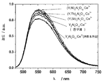
| Branigan | lntens./au | |
| PleWa | Winkler et a].(45) Date of Patent: Jan. 8, 2013 |
Legal Events
| Date | Code | Title | Description |
|---|---|---|---|
| PA0105 | International application |
St.27 status event code: A-0-1-A10-A15-nap-PA0105 |
|
| PG1501 | Laying open of application |
St.27 status event code: A-1-1-Q10-Q12-nap-PG1501 |
|
| A201 | Request for examination | ||
| P11-X000 | Amendment of application requested |
St.27 status event code: A-2-2-P10-P11-nap-X000 |
|
| P13-X000 | Application amended |
St.27 status event code: A-2-2-P10-P13-nap-X000 |
|
| PA0201 | Request for examination |
St.27 status event code: A-1-2-D10-D11-exm-PA0201 |
|
| E902 | Notification of reason for refusal | ||
| PE0902 | Notice of grounds for rejection |
St.27 status event code: A-1-2-D10-D21-exm-PE0902 |
|
| P11-X000 | Amendment of application requested |
St.27 status event code: A-2-2-P10-P11-nap-X000 |
|
| P13-X000 | Application amended |
St.27 status event code: A-2-2-P10-P13-nap-X000 |
|
| E701 | Decision to grant or registration of patent right | ||
| PE0701 | Decision of registration |
St.27 status event code: A-1-2-D10-D22-exm-PE0701 |
|
| GRNT | Written decision to grant | ||
| PR0701 | Registration of establishment |
St.27 status event code: A-2-4-F10-F11-exm-PR0701 |
|
| PR1002 | Payment of registration fee |
St.27 status event code: A-2-2-U10-U12-oth-PR1002 Fee payment year number: 1 |
|
| PG1601 | Publication of registration |
St.27 status event code: A-4-4-Q10-Q13-nap-PG1601 |
|
| FPAY | Annual fee payment |
Payment date: 20180104 Year of fee payment: 4 |
|
| PR1001 | Payment of annual fee |
St.27 status event code: A-4-4-U10-U11-oth-PR1001 Fee payment year number: 4 |
|
| LAPS | Lapse due to unpaid annual fee | ||
| PC1903 | Unpaid annual fee |
St.27 status event code: A-4-4-U10-U13-oth-PC1903 Not in force date: 20190122 Payment event data comment text: Termination Category : DEFAULT_OF_REGISTRATION_FEE |
|
| PC1903 | Unpaid annual fee |
St.27 status event code: N-4-6-H10-H13-oth-PC1903 Ip right cessation event data comment text: Termination Category : DEFAULT_OF_REGISTRATION_FEE Not in force date: 20190122 |
|
| R18-X000 | Changes to party contact information recorded |
St.27 status event code: A-5-5-R10-R18-oth-X000 |
|
| P22-X000 | Classification modified |
St.27 status event code: A-4-4-P10-P22-nap-X000 |