EP2075829B1 - A method and device for aligning components - Google Patents
A method and device for aligning components Download PDFInfo
- Publication number
- EP2075829B1 EP2075829B1 EP07150412A EP07150412A EP2075829B1 EP 2075829 B1 EP2075829 B1 EP 2075829B1 EP 07150412 A EP07150412 A EP 07150412A EP 07150412 A EP07150412 A EP 07150412A EP 2075829 B1 EP2075829 B1 EP 2075829B1
- Authority
- EP
- European Patent Office
- Prior art keywords
- component
- aligning
- nozzle
- pick
- aligning device
- Prior art date
- Legal status (The legal status is an assumption and is not a legal conclusion. Google has not performed a legal analysis and makes no representation as to the accuracy of the status listed.)
- Not-in-force
Links
Images

Classifications
-
- H—ELECTRICITY
- H01—ELECTRIC ELEMENTS
- H01L—SEMICONDUCTOR DEVICES NOT COVERED BY CLASS H10
- H01L21/00—Processes or apparatus adapted for the manufacture or treatment of semiconductor or solid state devices or of parts thereof
- H01L21/67—Apparatus specially adapted for handling semiconductor or electric solid state devices during manufacture or treatment thereof; Apparatus specially adapted for handling wafers during manufacture or treatment of semiconductor or electric solid state devices or components ; Apparatus not specifically provided for elsewhere
- H01L21/68—Apparatus specially adapted for handling semiconductor or electric solid state devices during manufacture or treatment thereof; Apparatus specially adapted for handling wafers during manufacture or treatment of semiconductor or electric solid state devices or components ; Apparatus not specifically provided for elsewhere for positioning, orientation or alignment
-
- H—ELECTRICITY
- H01—ELECTRIC ELEMENTS
- H01L—SEMICONDUCTOR DEVICES NOT COVERED BY CLASS H10
- H01L21/00—Processes or apparatus adapted for the manufacture or treatment of semiconductor or solid state devices or of parts thereof
- H01L21/67—Apparatus specially adapted for handling semiconductor or electric solid state devices during manufacture or treatment thereof; Apparatus specially adapted for handling wafers during manufacture or treatment of semiconductor or electric solid state devices or components ; Apparatus not specifically provided for elsewhere
- H01L21/67005—Apparatus not specifically provided for elsewhere
- H01L21/67011—Apparatus for manufacture or treatment
- H01L21/67144—Apparatus for mounting on conductive members, e.g. leadframes or conductors on insulating substrates
-
- H—ELECTRICITY
- H01—ELECTRIC ELEMENTS
- H01L—SEMICONDUCTOR DEVICES NOT COVERED BY CLASS H10
- H01L21/00—Processes or apparatus adapted for the manufacture or treatment of semiconductor or solid state devices or of parts thereof
- H01L21/67—Apparatus specially adapted for handling semiconductor or electric solid state devices during manufacture or treatment thereof; Apparatus specially adapted for handling wafers during manufacture or treatment of semiconductor or electric solid state devices or components ; Apparatus not specifically provided for elsewhere
- H01L21/67005—Apparatus not specifically provided for elsewhere
- H01L21/67242—Apparatus for monitoring, sorting or marking
- H01L21/67259—Position monitoring, e.g. misposition detection or presence detection
-
- H—ELECTRICITY
- H01—ELECTRIC ELEMENTS
- H01L—SEMICONDUCTOR DEVICES NOT COVERED BY CLASS H10
- H01L21/00—Processes or apparatus adapted for the manufacture or treatment of semiconductor or solid state devices or of parts thereof
- H01L21/67—Apparatus specially adapted for handling semiconductor or electric solid state devices during manufacture or treatment thereof; Apparatus specially adapted for handling wafers during manufacture or treatment of semiconductor or electric solid state devices or components ; Apparatus not specifically provided for elsewhere
- H01L21/683—Apparatus specially adapted for handling semiconductor or electric solid state devices during manufacture or treatment thereof; Apparatus specially adapted for handling wafers during manufacture or treatment of semiconductor or electric solid state devices or components ; Apparatus not specifically provided for elsewhere for supporting or gripping
- H01L21/6838—Apparatus specially adapted for handling semiconductor or electric solid state devices during manufacture or treatment thereof; Apparatus specially adapted for handling wafers during manufacture or treatment of semiconductor or electric solid state devices or components ; Apparatus not specifically provided for elsewhere for supporting or gripping with gripping and holding devices using a vacuum; Bernoulli devices
-
- G—PHYSICS
- G01—MEASURING; TESTING
- G01R—MEASURING ELECTRIC VARIABLES; MEASURING MAGNETIC VARIABLES
- G01R31/00—Arrangements for testing electric properties; Arrangements for locating electric faults; Arrangements for electrical testing characterised by what is being tested not provided for elsewhere
- G01R31/01—Subjecting similar articles in turn to test, e.g. "go/no-go" tests in mass production; Testing objects at points as they pass through a testing station
Definitions
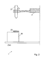
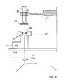
- FIG. 2 A schematic view of the first processing station 3a is shown in Fig. 2 .
- the pick-up nozzle 21, fastened on one extremity of the barrel 2 is connected to a source of pressure (not shown) able to apply in a controlled fashion a negative and possibly a positive pressure to the nozzle.
- the barrel 2 is positioned such as to align the pick-up nozzle 21 with the component 20 located underneath, for example on a conveyor shown schematically by the numeral 30.
- the pick-up nozzle 21 is brought in contact with the superior surface 22 of the component 20 and picks-up the component 20 by applying a negative pressure to the nozzle.
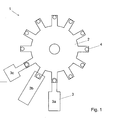
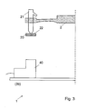
- the calibration tool may comprise an alignment jig (not shown), located in one of the turret processing stations 3, and employing a large recess that is tapered down to the dimensions of the component 20.
- the taper on the alignment jig then serves to essentially "funnel" the component 20 into a precise alignment with the pick-up nozzle 21 when the pick-up nozzle 21 picks-up the component 20.
- the pick-up nozzle 21 with the precisely aligned component 20 is then moved above the camera unit 40 in order to acquire a defined position value.
- Other type of calibration tools are also possible.
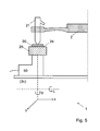
- both the pick-up nozzle 21 and the aligning device 25 are placed opposite in respect with both surfaces of the component 20 and remain in mechanical contact with the respective surfaces of the component 20.
Landscapes
- Engineering & Computer Science (AREA)
- Physics & Mathematics (AREA)
- Condensed Matter Physics & Semiconductors (AREA)
- General Physics & Mathematics (AREA)
- Manufacturing & Machinery (AREA)
- Computer Hardware Design (AREA)
- Microelectronics & Electronic Packaging (AREA)
- Power Engineering (AREA)
- Supply And Installment Of Electrical Components (AREA)
- Container, Conveyance, Adherence, Positioning, Of Wafer (AREA)
- Manipulator (AREA)
- Attitude Control For Articles On Conveyors (AREA)
Priority Applications (10)
| Application Number | Priority Date | Filing Date | Title |
|---|---|---|---|
| EP07150412A EP2075829B1 (en) | 2007-12-24 | 2007-12-24 | A method and device for aligning components |
| AT07150412T ATE528792T1 (de) | 2007-12-24 | 2007-12-24 | Verfahren und vorrichtung zur ausrichtung von komponenten |
| CN2008801225452A CN101919039B (zh) | 2007-12-24 | 2008-12-17 | 对准元件的方法和设备 |
| PCT/EP2008/067752 WO2009080652A1 (en) | 2007-12-24 | 2008-12-17 | A method and device for aligning components |
| MX2010006994A MX2010006994A (es) | 2007-12-24 | 2008-12-17 | Un metodo y dispositivo para alinear componentes. |
| KR1020107016432A KR101448076B1 (ko) | 2007-12-24 | 2008-12-17 | 부품들을 정렬하기 위한 방법 및 장치 |
| MYPI2010002996A MY147294A (en) | 2007-12-24 | 2008-12-17 | A method and device for aligning components |
| TW097150025A TWI483340B (zh) | 2007-12-24 | 2008-12-22 | 組件對準方法及裝置 |
| US12/819,300 US8550766B2 (en) | 2007-12-24 | 2010-06-21 | Method and device for aligning components |
| HK11102418.7A HK1148387A1 (en) | 2007-12-24 | 2011-03-10 | A method and device for aligning components |
Applications Claiming Priority (1)
| Application Number | Priority Date | Filing Date | Title |
|---|---|---|---|
| EP07150412A EP2075829B1 (en) | 2007-12-24 | 2007-12-24 | A method and device for aligning components |
Publications (2)
| Publication Number | Publication Date |
|---|---|
| EP2075829A1 EP2075829A1 (en) | 2009-07-01 |
| EP2075829B1 true EP2075829B1 (en) | 2011-10-12 |
Family
ID=39332222
Family Applications (1)
| Application Number | Title | Priority Date | Filing Date |
|---|---|---|---|
| EP07150412A Not-in-force EP2075829B1 (en) | 2007-12-24 | 2007-12-24 | A method and device for aligning components |
Country Status (10)
| Country | Link |
|---|---|
| US (1) | US8550766B2 (es) |
| EP (1) | EP2075829B1 (es) |
| KR (1) | KR101448076B1 (es) |
| CN (1) | CN101919039B (es) |
| AT (1) | ATE528792T1 (es) |
| HK (1) | HK1148387A1 (es) |
| MX (1) | MX2010006994A (es) |
| MY (1) | MY147294A (es) |
| TW (1) | TWI483340B (es) |
| WO (1) | WO2009080652A1 (es) |
Cited By (5)
| Publication number | Priority date | Publication date | Assignee | Title |
|---|---|---|---|---|
| TWI467043B (es) * | 2013-02-01 | 2015-01-01 | ||
| DE102017008869B3 (de) | 2017-09-21 | 2018-10-25 | Mühlbauer Gmbh & Co. Kg | Bauteilzentrierung |
| DE102019125127A1 (de) * | 2019-09-18 | 2021-03-18 | Mühlbauer Gmbh & Co. Kg | Bauteilhandhabung, Bauteilinspektion |
| WO2021052745A1 (de) | 2019-09-18 | 2021-03-25 | Muehlbauer GmbH & Co. KG | Bauteilhandhabungsvorrichtung mit bauteilinspektionsvorrichtung |
| WO2022233521A1 (de) | 2021-05-07 | 2022-11-10 | Muehlbauer GmbH & Co. KG | Optische bauteilinspektion |
Families Citing this family (16)
| Publication number | Priority date | Publication date | Assignee | Title |
|---|---|---|---|---|
| GB2471712A (en) * | 2009-07-10 | 2011-01-12 | De Beers Centenary AG | Gemstone alignment system |
| JP5299379B2 (ja) * | 2010-08-17 | 2013-09-25 | パナソニック株式会社 | 部品実装装置および部品検出方法 |
| JP5299380B2 (ja) * | 2010-08-17 | 2013-09-25 | パナソニック株式会社 | 部品実装装置および部品検出方法 |
| DE102011013369A1 (de) * | 2010-12-30 | 2012-07-05 | Osram Opto Semiconductors Gmbh | Verfahren zum Herstellen einer Mehrzahl von Halbleiterbauelementen |
| EP2658958B1 (en) * | 2011-03-18 | 2017-05-03 | Siemens Healthcare Diagnostics Inc. | Methods and systems for calibration of a positional orientation between a sample container and nozzle tip |
| US9044812B2 (en) | 2011-08-03 | 2015-06-02 | General Electric Company | Jig and method for modifying casing in turbine system |
| SG11201400399UA (en) * | 2011-12-07 | 2014-04-28 | Ismeca Semiconductor Holding | A component handling assembly |
| US8919528B2 (en) * | 2012-07-13 | 2014-12-30 | Hewlett-Packard Industrial Printing Ltd. | Nozzled device to align a substrate on a surface |
| KR101479667B1 (ko) * | 2014-04-21 | 2015-01-07 | 주식회사 디앤씨 | 압력 조절 장치 및 이를 이용한 피처리물 이송 방법 |
| KR101687191B1 (ko) * | 2015-08-17 | 2016-12-19 | 비케이전자 주식회사 | 전자부품 실장장치 |
| MY192110A (en) * | 2018-07-26 | 2022-07-28 | Mi Equipment M Sdn Bhd | Method for automatic alignment of an electronic component during die sorting process |
| WO2020203948A1 (ja) * | 2019-04-04 | 2020-10-08 | アキム株式会社 | 部品搬送処理装置 |
| JP7291577B2 (ja) * | 2019-08-28 | 2023-06-15 | 芝浦メカトロニクス株式会社 | 移送装置および実装装置 |
| TWI741748B (zh) * | 2020-08-20 | 2021-10-01 | 鴻勁精密股份有限公司 | 接合機構及其應用之作業設備 |
| WO2022046566A1 (en) * | 2020-08-27 | 2022-03-03 | Mrsi Systems Llc | Self-aligning tip |
| CN113877845A (zh) * | 2021-10-28 | 2022-01-04 | 浙江庆鑫科技有限公司 | 一种压力补偿装置及方法 |
Family Cites Families (10)
| Publication number | Priority date | Publication date | Assignee | Title |
|---|---|---|---|---|
| JPH0697718B2 (ja) | 1989-11-18 | 1994-11-30 | 太陽誘電株式会社 | チップ状電子部品マウント方法及び装置 |
| US5133926A (en) * | 1991-04-18 | 1992-07-28 | Westinghouse Electric Corp. | Extended burnup top nozzle for a nuclear fuel assembly |
| JP3258026B2 (ja) * | 1995-07-12 | 2002-02-18 | 松下電器産業株式会社 | 電子部品実装方法及び装置 |
| JP3935632B2 (ja) | 1998-10-27 | 2007-06-27 | 松下電器産業株式会社 | 電子部品の実装方法 |
| JP3719182B2 (ja) | 2001-09-28 | 2005-11-24 | 松下電器産業株式会社 | 電子部品実装装置および電子部品実装方法 |
| JP3861710B2 (ja) | 2002-02-15 | 2006-12-20 | 松下電器産業株式会社 | 電子部品供給装置および電子部品実装装置 |
| US7306695B2 (en) | 2003-04-10 | 2007-12-11 | Matsushita Electric Industrial Co., Ltd. | Apparatus and method for picking up semiconductor chip |
| US7222654B2 (en) * | 2004-04-30 | 2007-05-29 | The Procter & Gamble Company | Apparatus for producing elastomeric nonwoven laminates |
| JP4516354B2 (ja) | 2004-05-17 | 2010-08-04 | パナソニック株式会社 | 部品供給方法 |
| US7207430B2 (en) * | 2004-10-25 | 2007-04-24 | Ui Holding Company | Vacuum gripper for handling small components |
-
2007
- 2007-12-24 AT AT07150412T patent/ATE528792T1/de active
- 2007-12-24 EP EP07150412A patent/EP2075829B1/en not_active Not-in-force
-
2008
- 2008-12-17 KR KR1020107016432A patent/KR101448076B1/ko active IP Right Grant
- 2008-12-17 CN CN2008801225452A patent/CN101919039B/zh active Active
- 2008-12-17 MX MX2010006994A patent/MX2010006994A/es active IP Right Grant
- 2008-12-17 MY MYPI2010002996A patent/MY147294A/en unknown
- 2008-12-17 WO PCT/EP2008/067752 patent/WO2009080652A1/en active Application Filing
- 2008-12-22 TW TW097150025A patent/TWI483340B/zh active
-
2010
- 2010-06-21 US US12/819,300 patent/US8550766B2/en active Active
-
2011
- 2011-03-10 HK HK11102418.7A patent/HK1148387A1/xx not_active IP Right Cessation
Cited By (10)
| Publication number | Priority date | Publication date | Assignee | Title |
|---|---|---|---|---|
| TWI467043B (es) * | 2013-02-01 | 2015-01-01 | ||
| DE102017008869B3 (de) | 2017-09-21 | 2018-10-25 | Mühlbauer Gmbh & Co. Kg | Bauteilzentrierung |
| WO2019057469A1 (de) | 2017-09-21 | 2019-03-28 | Muehlbauer GmbH & Co. KG | Vorrichtung zur ausrichtung und optischen inspektion eines halbleiterbauteils |
| US11152243B2 (en) | 2017-09-21 | 2021-10-19 | Muehlbauer GmbH & Co. KG | Device for aligning and optically inspecting a semiconductor component |
| DE102019125127A1 (de) * | 2019-09-18 | 2021-03-18 | Mühlbauer Gmbh & Co. Kg | Bauteilhandhabung, Bauteilinspektion |
| WO2021052745A1 (de) | 2019-09-18 | 2021-03-25 | Muehlbauer GmbH & Co. KG | Bauteilhandhabungsvorrichtung mit bauteilinspektionsvorrichtung |
| WO2021052756A1 (de) | 2019-09-18 | 2021-03-25 | Muehlbauer GmbH & Co. KG | Bauteilhandhabung mit bauteilinspektion |
| US11856705B2 (en) | 2019-09-18 | 2023-12-26 | Muehlbauer GmbH & Co. KG | Apparatus for handling components |
| WO2022233521A1 (de) | 2021-05-07 | 2022-11-10 | Muehlbauer GmbH & Co. KG | Optische bauteilinspektion |
| DE102021111953A1 (de) | 2021-05-07 | 2022-11-10 | Mühlbauer Gmbh & Co. Kg | Optische Bauteilinspektion |
Also Published As
| Publication number | Publication date |
|---|---|
| KR20100110835A (ko) | 2010-10-13 |
| HK1148387A1 (en) | 2011-09-02 |
| CN101919039A (zh) | 2010-12-15 |
| ATE528792T1 (de) | 2011-10-15 |
| TW200935551A (en) | 2009-08-16 |
| US8550766B2 (en) | 2013-10-08 |
| CN101919039B (zh) | 2012-12-05 |
| MY147294A (en) | 2012-11-30 |
| MX2010006994A (es) | 2010-08-25 |
| KR101448076B1 (ko) | 2014-10-07 |
| EP2075829A1 (en) | 2009-07-01 |
| TWI483340B (zh) | 2015-05-01 |
| WO2009080652A1 (en) | 2009-07-02 |
| US20100254788A1 (en) | 2010-10-07 |
Similar Documents
| Publication | Publication Date | Title |
|---|---|---|
| EP2075829B1 (en) | A method and device for aligning components | |
| US20180059176A1 (en) | Offline vision assist method and apparatus for integrated circuit device vision alignment | |
| JP2821046B2 (ja) | 半導体素子用特性検査装置 | |
| KR100261935B1 (ko) | 전자다이 자동배치 방법 및 장치 | |
| TWI673806B (zh) | 熱壓鍵合裝置 | |
| CN106981444B (zh) | 热压键合装置 | |
| TW201430356A (zh) | 電子元件作業單元、作業方法及其應用之作業設備 | |
| WO2015083414A1 (ja) | 電子部品搬送装置 | |
| KR102355572B1 (ko) | 검사 장치, 검사 시스템, 및 위치 맞춤 방법 | |
| JP4984259B2 (ja) | サンプル保持機構 | |
| JP7102305B2 (ja) | ダイボンディング装置および半導体装置の製造方法 | |
| CN113074923A (zh) | 用于抓持装置的真空吸头的状态控制的检查设备和方法 | |
| TWI545329B (zh) | An electronic component operating device, a working method, and a working device for its application | |
| JP2648371B2 (ja) | Tabディバイスの検査方法及びそれに用いるtabディバイス用キャリア並びに測定モジュール及びインサート装置 | |
| EP3654747B1 (en) | Adjustment jig and alignment method | |
| WO2014033961A1 (ja) | 部品実装装置 | |
| JP4301393B2 (ja) | 半導体装置の製造装置 | |
| USRE33641E (en) | Method and apparatus for proper registration of mating parts | |
| KR20240009643A (ko) | 프로브 본딩장치 및 이를 이용한 프로브 본딩방법 | |
| KR20240009647A (ko) | 프로브 본딩장치 및 이를 이용한 프로브 본딩방법 | |
| CN114062382A (zh) | 一种检测系统及检测方法 | |
| KR20240009653A (ko) | 프로브 본딩장치 및 이를 이용한 프로브 본딩방법 | |
| KR20220010964A (ko) | 반도체 스트립 정렬 방법 및 반도체 스트립 절단 방법 | |
| KR20230125518A (ko) | 인쇄회로기판 전기검사장치 및 전기검사방법 | |
| CN118235234A (zh) | 工件检查装置 |
Legal Events
| Date | Code | Title | Description |
|---|---|---|---|
| PUAI | Public reference made under article 153(3) epc to a published international application that has entered the european phase |
Free format text: ORIGINAL CODE: 0009012 |
|
| AK | Designated contracting states |
Kind code of ref document: A1 Designated state(s): AT BE BG CH CY CZ DE DK EE ES FI FR GB GR HU IE IS IT LI LT LU LV MC MT NL PL PT RO SE SI SK TR |
|
| AX | Request for extension of the european patent |
Extension state: AL BA HR MK RS |
|
| 17P | Request for examination filed |
Effective date: 20090928 |
|
| 17Q | First examination report despatched |
Effective date: 20091117 |
|
| AKX | Designation fees paid |
Designated state(s): AT BE BG CH CY CZ DE DK EE ES FI FR GB GR HU IE IS IT LI LT LU LV MC MT NL PL PT RO SE SI SK TR |
|
| GRAP | Despatch of communication of intention to grant a patent |
Free format text: ORIGINAL CODE: EPIDOSNIGR1 |
|
| GRAS | Grant fee paid |
Free format text: ORIGINAL CODE: EPIDOSNIGR3 |
|
| GRAA | (expected) grant |
Free format text: ORIGINAL CODE: 0009210 |
|
| AK | Designated contracting states |
Kind code of ref document: B1 Designated state(s): AT BE BG CH CY CZ DE DK EE ES FI FR GB GR HU IE IS IT LI LT LU LV MC MT NL PL PT RO SE SI SK TR |
|
| REG | Reference to a national code |
Ref country code: GB Ref legal event code: FG4D |
|
| REG | Reference to a national code |
Ref country code: CH Ref legal event code: EP |
|
| REG | Reference to a national code |
Ref country code: IE Ref legal event code: FG4D |
|
| REG | Reference to a national code |
Ref country code: DE Ref legal event code: R096 Ref document number: 602007017741 Country of ref document: DE Effective date: 20111208 |
|
| REG | Reference to a national code |
Ref country code: NL Ref legal event code: VDEP Effective date: 20111012 |
|
| LTIE | Lt: invalidation of european patent or patent extension |
Effective date: 20111012 |
|
| PG25 | Lapsed in a contracting state [announced via postgrant information from national office to epo] |
Ref country code: IS Free format text: LAPSE BECAUSE OF FAILURE TO SUBMIT A TRANSLATION OF THE DESCRIPTION OR TO PAY THE FEE WITHIN THE PRESCRIBED TIME-LIMIT Effective date: 20120212 Ref country code: LT Free format text: LAPSE BECAUSE OF FAILURE TO SUBMIT A TRANSLATION OF THE DESCRIPTION OR TO PAY THE FEE WITHIN THE PRESCRIBED TIME-LIMIT Effective date: 20111012 Ref country code: BE Free format text: LAPSE BECAUSE OF FAILURE TO SUBMIT A TRANSLATION OF THE DESCRIPTION OR TO PAY THE FEE WITHIN THE PRESCRIBED TIME-LIMIT Effective date: 20111012 |
|
| PG25 | Lapsed in a contracting state [announced via postgrant information from national office to epo] |
Ref country code: SE Free format text: LAPSE BECAUSE OF FAILURE TO SUBMIT A TRANSLATION OF THE DESCRIPTION OR TO PAY THE FEE WITHIN THE PRESCRIBED TIME-LIMIT Effective date: 20111012 Ref country code: PT Free format text: LAPSE BECAUSE OF FAILURE TO SUBMIT A TRANSLATION OF THE DESCRIPTION OR TO PAY THE FEE WITHIN THE PRESCRIBED TIME-LIMIT Effective date: 20120213 Ref country code: NL Free format text: LAPSE BECAUSE OF FAILURE TO SUBMIT A TRANSLATION OF THE DESCRIPTION OR TO PAY THE FEE WITHIN THE PRESCRIBED TIME-LIMIT Effective date: 20111012 Ref country code: LV Free format text: LAPSE BECAUSE OF FAILURE TO SUBMIT A TRANSLATION OF THE DESCRIPTION OR TO PAY THE FEE WITHIN THE PRESCRIBED TIME-LIMIT Effective date: 20111012 Ref country code: GR Free format text: LAPSE BECAUSE OF FAILURE TO SUBMIT A TRANSLATION OF THE DESCRIPTION OR TO PAY THE FEE WITHIN THE PRESCRIBED TIME-LIMIT Effective date: 20120113 Ref country code: SI Free format text: LAPSE BECAUSE OF FAILURE TO SUBMIT A TRANSLATION OF THE DESCRIPTION OR TO PAY THE FEE WITHIN THE PRESCRIBED TIME-LIMIT Effective date: 20111012 |
|
| PG25 | Lapsed in a contracting state [announced via postgrant information from national office to epo] |
Ref country code: CY Free format text: LAPSE BECAUSE OF FAILURE TO SUBMIT A TRANSLATION OF THE DESCRIPTION OR TO PAY THE FEE WITHIN THE PRESCRIBED TIME-LIMIT Effective date: 20111012 |
|
| PG25 | Lapsed in a contracting state [announced via postgrant information from national office to epo] |
Ref country code: EE Free format text: LAPSE BECAUSE OF FAILURE TO SUBMIT A TRANSLATION OF THE DESCRIPTION OR TO PAY THE FEE WITHIN THE PRESCRIBED TIME-LIMIT Effective date: 20111012 Ref country code: SK Free format text: LAPSE BECAUSE OF FAILURE TO SUBMIT A TRANSLATION OF THE DESCRIPTION OR TO PAY THE FEE WITHIN THE PRESCRIBED TIME-LIMIT Effective date: 20111012 Ref country code: CZ Free format text: LAPSE BECAUSE OF FAILURE TO SUBMIT A TRANSLATION OF THE DESCRIPTION OR TO PAY THE FEE WITHIN THE PRESCRIBED TIME-LIMIT Effective date: 20111012 Ref country code: DK Free format text: LAPSE BECAUSE OF FAILURE TO SUBMIT A TRANSLATION OF THE DESCRIPTION OR TO PAY THE FEE WITHIN THE PRESCRIBED TIME-LIMIT Effective date: 20111012 Ref country code: MC Free format text: LAPSE BECAUSE OF NON-PAYMENT OF DUE FEES Effective date: 20111231 Ref country code: BG Free format text: LAPSE BECAUSE OF FAILURE TO SUBMIT A TRANSLATION OF THE DESCRIPTION OR TO PAY THE FEE WITHIN THE PRESCRIBED TIME-LIMIT Effective date: 20120112 |
|
| REG | Reference to a national code |
Ref country code: CH Ref legal event code: PL |
|
| PLBE | No opposition filed within time limit |
Free format text: ORIGINAL CODE: 0009261 |
|
| STAA | Information on the status of an ep patent application or granted ep patent |
Free format text: STATUS: NO OPPOSITION FILED WITHIN TIME LIMIT |
|
| PG25 | Lapsed in a contracting state [announced via postgrant information from national office to epo] |
Ref country code: PL Free format text: LAPSE BECAUSE OF FAILURE TO SUBMIT A TRANSLATION OF THE DESCRIPTION OR TO PAY THE FEE WITHIN THE PRESCRIBED TIME-LIMIT Effective date: 20111012 Ref country code: RO Free format text: LAPSE BECAUSE OF FAILURE TO SUBMIT A TRANSLATION OF THE DESCRIPTION OR TO PAY THE FEE WITHIN THE PRESCRIBED TIME-LIMIT Effective date: 20111012 |
|
| 26N | No opposition filed |
Effective date: 20120713 |
|
| REG | Reference to a national code |
Ref country code: IE Ref legal event code: MM4A |
|
| PG25 | Lapsed in a contracting state [announced via postgrant information from national office to epo] |
Ref country code: CH Free format text: LAPSE BECAUSE OF NON-PAYMENT OF DUE FEES Effective date: 20111231 Ref country code: LI Free format text: LAPSE BECAUSE OF NON-PAYMENT OF DUE FEES Effective date: 20111231 Ref country code: IE Free format text: LAPSE BECAUSE OF NON-PAYMENT OF DUE FEES Effective date: 20111224 |
|
| REG | Reference to a national code |
Ref country code: DE Ref legal event code: R097 Ref document number: 602007017741 Country of ref document: DE Effective date: 20120713 |
|
| PG25 | Lapsed in a contracting state [announced via postgrant information from national office to epo] |
Ref country code: ES Free format text: LAPSE BECAUSE OF FAILURE TO SUBMIT A TRANSLATION OF THE DESCRIPTION OR TO PAY THE FEE WITHIN THE PRESCRIBED TIME-LIMIT Effective date: 20120123 |
|
| PG25 | Lapsed in a contracting state [announced via postgrant information from national office to epo] |
Ref country code: LU Free format text: LAPSE BECAUSE OF NON-PAYMENT OF DUE FEES Effective date: 20111224 |
|
| PG25 | Lapsed in a contracting state [announced via postgrant information from national office to epo] |
Ref country code: FI Free format text: LAPSE BECAUSE OF FAILURE TO SUBMIT A TRANSLATION OF THE DESCRIPTION OR TO PAY THE FEE WITHIN THE PRESCRIBED TIME-LIMIT Effective date: 20111012 |
|
| PG25 | Lapsed in a contracting state [announced via postgrant information from national office to epo] |
Ref country code: TR Free format text: LAPSE BECAUSE OF FAILURE TO SUBMIT A TRANSLATION OF THE DESCRIPTION OR TO PAY THE FEE WITHIN THE PRESCRIBED TIME-LIMIT Effective date: 20111012 |
|
| PG25 | Lapsed in a contracting state [announced via postgrant information from national office to epo] |
Ref country code: HU Free format text: LAPSE BECAUSE OF FAILURE TO SUBMIT A TRANSLATION OF THE DESCRIPTION OR TO PAY THE FEE WITHIN THE PRESCRIBED TIME-LIMIT Effective date: 20111012 |
|
| PGFP | Annual fee paid to national office [announced via postgrant information from national office to epo] |
Ref country code: AT Payment date: 20131211 Year of fee payment: 7 |
|
| PGFP | Annual fee paid to national office [announced via postgrant information from national office to epo] |
Ref country code: IT Payment date: 20131223 Year of fee payment: 7 |
|
| PGFP | Annual fee paid to national office [announced via postgrant information from national office to epo] |
Ref country code: GB Payment date: 20141219 Year of fee payment: 8 |
|
| REG | Reference to a national code |
Ref country code: AT Ref legal event code: MM01 Ref document number: 528792 Country of ref document: AT Kind code of ref document: T Effective date: 20141224 |
|
| PGFP | Annual fee paid to national office [announced via postgrant information from national office to epo] |
Ref country code: MT Payment date: 20130425 Year of fee payment: 7 |
|
| PG25 | Lapsed in a contracting state [announced via postgrant information from national office to epo] |
Ref country code: AT Free format text: LAPSE BECAUSE OF NON-PAYMENT OF DUE FEES Effective date: 20141224 |
|
| REG | Reference to a national code |
Ref country code: FR Ref legal event code: PLFP Year of fee payment: 9 |
|
| PG25 | Lapsed in a contracting state [announced via postgrant information from national office to epo] |
Ref country code: IT Free format text: LAPSE BECAUSE OF NON-PAYMENT OF DUE FEES Effective date: 20141224 |
|
| PG25 | Lapsed in a contracting state [announced via postgrant information from national office to epo] |
Ref country code: MT Free format text: LAPSE BECAUSE OF NON-PAYMENT OF DUE FEES Effective date: 20141231 |
|
| GBPC | Gb: european patent ceased through non-payment of renewal fee |
Effective date: 20151224 |
|
| PG25 | Lapsed in a contracting state [announced via postgrant information from national office to epo] |
Ref country code: GB Free format text: LAPSE BECAUSE OF NON-PAYMENT OF DUE FEES Effective date: 20151224 |
|
| REG | Reference to a national code |
Ref country code: FR Ref legal event code: PLFP Year of fee payment: 10 |
|
| REG | Reference to a national code |
Ref country code: FR Ref legal event code: PLFP Year of fee payment: 11 |
|
| PG25 | Lapsed in a contracting state [announced via postgrant information from national office to epo] |
Ref country code: MT Free format text: LAPSE BECAUSE OF NON-PAYMENT OF DUE FEES Effective date: 20141224 |
|
| PGFP | Annual fee paid to national office [announced via postgrant information from national office to epo] |
Ref country code: DE Payment date: 20191210 Year of fee payment: 13 |
|
| PGFP | Annual fee paid to national office [announced via postgrant information from national office to epo] |
Ref country code: FR Payment date: 20191220 Year of fee payment: 13 |
|
| REG | Reference to a national code |
Ref country code: DE Ref legal event code: R082 Ref document number: 602007017741 Country of ref document: DE Representative=s name: BECK & ROESSIG - EUROPEAN PATENT ATTORNEYS, DE |
|
| REG | Reference to a national code |
Ref country code: DE Ref legal event code: R119 Ref document number: 602007017741 Country of ref document: DE |
|
| PG25 | Lapsed in a contracting state [announced via postgrant information from national office to epo] |
Ref country code: FR Free format text: LAPSE BECAUSE OF NON-PAYMENT OF DUE FEES Effective date: 20201231 |
|
| PG25 | Lapsed in a contracting state [announced via postgrant information from national office to epo] |
Ref country code: DE Free format text: LAPSE BECAUSE OF NON-PAYMENT OF DUE FEES Effective date: 20210701 |