EP2037722B1 - Printed circuit board, display apparatus having a printed circuit board and method of manufacturing the printed circuit board - Google Patents
Printed circuit board, display apparatus having a printed circuit board and method of manufacturing the printed circuit board Download PDFInfo
- Publication number
- EP2037722B1 EP2037722B1 EP08006205A EP08006205A EP2037722B1 EP 2037722 B1 EP2037722 B1 EP 2037722B1 EP 08006205 A EP08006205 A EP 08006205A EP 08006205 A EP08006205 A EP 08006205A EP 2037722 B1 EP2037722 B1 EP 2037722B1
- Authority
- EP
- European Patent Office
- Prior art keywords
- pattern
- line
- pattern structure
- line pattern
- ground
- Prior art date
- Legal status (The legal status is an assumption and is not a legal conclusion. Google has not performed a legal analysis and makes no representation as to the accuracy of the status listed.)
- Active
Links
Images


Classifications
-
- H—ELECTRICITY
- H05—ELECTRIC TECHNIQUES NOT OTHERWISE PROVIDED FOR
- H05K—PRINTED CIRCUITS; CASINGS OR CONSTRUCTIONAL DETAILS OF ELECTRIC APPARATUS; MANUFACTURE OF ASSEMBLAGES OF ELECTRICAL COMPONENTS
- H05K1/00—Printed circuits
- H05K1/02—Details
- H05K1/0213—Electrical arrangements not otherwise provided for
- H05K1/0216—Reduction of cross-talk, noise or electromagnetic interference
- H05K1/0218—Reduction of cross-talk, noise or electromagnetic interference by printed shielding conductors, ground planes or power plane
- H05K1/0219—Printed shielding conductors for shielding around or between signal conductors, e.g. coplanar or coaxial printed shielding conductors
-
- H—ELECTRICITY
- H05—ELECTRIC TECHNIQUES NOT OTHERWISE PROVIDED FOR
- H05K—PRINTED CIRCUITS; CASINGS OR CONSTRUCTIONAL DETAILS OF ELECTRIC APPARATUS; MANUFACTURE OF ASSEMBLAGES OF ELECTRICAL COMPONENTS
- H05K1/00—Printed circuits
- H05K1/02—Details
-
- G—PHYSICS
- G09—EDUCATION; CRYPTOGRAPHY; DISPLAY; ADVERTISING; SEALS
- G09G—ARRANGEMENTS OR CIRCUITS FOR CONTROL OF INDICATING DEVICES USING STATIC MEANS TO PRESENT VARIABLE INFORMATION
- G09G3/00—Control arrangements or circuits, of interest only in connection with visual indicators other than cathode-ray tubes
- G09G3/20—Control arrangements or circuits, of interest only in connection with visual indicators other than cathode-ray tubes for presentation of an assembly of a number of characters, e.g. a page, by composing the assembly by combination of individual elements arranged in a matrix no fixed position being assigned to or needed to be assigned to the individual characters or partial characters
- G09G3/34—Control arrangements or circuits, of interest only in connection with visual indicators other than cathode-ray tubes for presentation of an assembly of a number of characters, e.g. a page, by composing the assembly by combination of individual elements arranged in a matrix no fixed position being assigned to or needed to be assigned to the individual characters or partial characters by control of light from an independent source
- G09G3/36—Control arrangements or circuits, of interest only in connection with visual indicators other than cathode-ray tubes for presentation of an assembly of a number of characters, e.g. a page, by composing the assembly by combination of individual elements arranged in a matrix no fixed position being assigned to or needed to be assigned to the individual characters or partial characters by control of light from an independent source using liquid crystals
- G09G3/3611—Control of matrices with row and column drivers
- G09G3/3696—Generation of voltages supplied to electrode drivers
-
- H—ELECTRICITY
- H05—ELECTRIC TECHNIQUES NOT OTHERWISE PROVIDED FOR
- H05K—PRINTED CIRCUITS; CASINGS OR CONSTRUCTIONAL DETAILS OF ELECTRIC APPARATUS; MANUFACTURE OF ASSEMBLAGES OF ELECTRICAL COMPONENTS
- H05K1/00—Printed circuits
- H05K1/02—Details
- H05K1/0213—Electrical arrangements not otherwise provided for
- H05K1/0216—Reduction of cross-talk, noise or electromagnetic interference
- H05K1/0218—Reduction of cross-talk, noise or electromagnetic interference by printed shielding conductors, ground planes or power plane
-
- H—ELECTRICITY
- H05—ELECTRIC TECHNIQUES NOT OTHERWISE PROVIDED FOR
- H05K—PRINTED CIRCUITS; CASINGS OR CONSTRUCTIONAL DETAILS OF ELECTRIC APPARATUS; MANUFACTURE OF ASSEMBLAGES OF ELECTRICAL COMPONENTS
- H05K1/00—Printed circuits
- H05K1/02—Details
- H05K1/0213—Electrical arrangements not otherwise provided for
- H05K1/0237—High frequency adaptations
-
- G—PHYSICS
- G09—EDUCATION; CRYPTOGRAPHY; DISPLAY; ADVERTISING; SEALS
- G09G—ARRANGEMENTS OR CIRCUITS FOR CONTROL OF INDICATING DEVICES USING STATIC MEANS TO PRESENT VARIABLE INFORMATION
- G09G2330/00—Aspects of power supply; Aspects of display protection and defect management
- G09G2330/06—Handling electromagnetic interferences [EMI], covering emitted as well as received electromagnetic radiation
-
- H—ELECTRICITY
- H05—ELECTRIC TECHNIQUES NOT OTHERWISE PROVIDED FOR
- H05K—PRINTED CIRCUITS; CASINGS OR CONSTRUCTIONAL DETAILS OF ELECTRIC APPARATUS; MANUFACTURE OF ASSEMBLAGES OF ELECTRICAL COMPONENTS
- H05K1/00—Printed circuits
- H05K1/02—Details
- H05K1/0296—Conductive pattern lay-out details not covered by sub groups H05K1/02 - H05K1/0295
- H05K1/0298—Multilayer circuits
-
- H—ELECTRICITY
- H05—ELECTRIC TECHNIQUES NOT OTHERWISE PROVIDED FOR
- H05K—PRINTED CIRCUITS; CASINGS OR CONSTRUCTIONAL DETAILS OF ELECTRIC APPARATUS; MANUFACTURE OF ASSEMBLAGES OF ELECTRICAL COMPONENTS
- H05K2201/00—Indexing scheme relating to printed circuits covered by H05K1/00
- H05K2201/07—Electric details
- H05K2201/0707—Shielding
- H05K2201/0715—Shielding provided by an outer layer of PCB
-
- H—ELECTRICITY
- H05—ELECTRIC TECHNIQUES NOT OTHERWISE PROVIDED FOR
- H05K—PRINTED CIRCUITS; CASINGS OR CONSTRUCTIONAL DETAILS OF ELECTRIC APPARATUS; MANUFACTURE OF ASSEMBLAGES OF ELECTRICAL COMPONENTS
- H05K2201/00—Indexing scheme relating to printed circuits covered by H05K1/00
- H05K2201/09—Shape and layout
- H05K2201/09209—Shape and layout details of conductors
- H05K2201/09218—Conductive traces
- H05K2201/09236—Parallel layout
-
- H—ELECTRICITY
- H05—ELECTRIC TECHNIQUES NOT OTHERWISE PROVIDED FOR
- H05K—PRINTED CIRCUITS; CASINGS OR CONSTRUCTIONAL DETAILS OF ELECTRIC APPARATUS; MANUFACTURE OF ASSEMBLAGES OF ELECTRICAL COMPONENTS
- H05K2201/00—Indexing scheme relating to printed circuits covered by H05K1/00
- H05K2201/09—Shape and layout
- H05K2201/09209—Shape and layout details of conductors
- H05K2201/0929—Conductive planes
- H05K2201/09336—Signal conductors in same plane as power plane
-
- H—ELECTRICITY
- H05—ELECTRIC TECHNIQUES NOT OTHERWISE PROVIDED FOR
- H05K—PRINTED CIRCUITS; CASINGS OR CONSTRUCTIONAL DETAILS OF ELECTRIC APPARATUS; MANUFACTURE OF ASSEMBLAGES OF ELECTRICAL COMPONENTS
- H05K2201/00—Indexing scheme relating to printed circuits covered by H05K1/00
- H05K2201/09—Shape and layout
- H05K2201/09209—Shape and layout details of conductors
- H05K2201/09654—Shape and layout details of conductors covering at least two types of conductors provided for in H05K2201/09218 - H05K2201/095
- H05K2201/09672—Superposed layout, i.e. in different planes
-
- Y—GENERAL TAGGING OF NEW TECHNOLOGICAL DEVELOPMENTS; GENERAL TAGGING OF CROSS-SECTIONAL TECHNOLOGIES SPANNING OVER SEVERAL SECTIONS OF THE IPC; TECHNICAL SUBJECTS COVERED BY FORMER USPC CROSS-REFERENCE ART COLLECTIONS [XRACs] AND DIGESTS
- Y10—TECHNICAL SUBJECTS COVERED BY FORMER USPC
- Y10T—TECHNICAL SUBJECTS COVERED BY FORMER US CLASSIFICATION
- Y10T29/00—Metal working
- Y10T29/49—Method of mechanical manufacture
- Y10T29/49002—Electrical device making
- Y10T29/49117—Conductor or circuit manufacturing
- Y10T29/49124—On flat or curved insulated base, e.g., printed circuit, etc.
- Y10T29/49126—Assembling bases
-
- Y—GENERAL TAGGING OF NEW TECHNOLOGICAL DEVELOPMENTS; GENERAL TAGGING OF CROSS-SECTIONAL TECHNOLOGIES SPANNING OVER SEVERAL SECTIONS OF THE IPC; TECHNICAL SUBJECTS COVERED BY FORMER USPC CROSS-REFERENCE ART COLLECTIONS [XRACs] AND DIGESTS
- Y10—TECHNICAL SUBJECTS COVERED BY FORMER USPC
- Y10T—TECHNICAL SUBJECTS COVERED BY FORMER US CLASSIFICATION
- Y10T29/00—Metal working
- Y10T29/49—Method of mechanical manufacture
- Y10T29/49002—Electrical device making
- Y10T29/49117—Conductor or circuit manufacturing
- Y10T29/49124—On flat or curved insulated base, e.g., printed circuit, etc.
- Y10T29/4913—Assembling to base an electrical component, e.g., capacitor, etc.
- Y10T29/49144—Assembling to base an electrical component, e.g., capacitor, etc. by metal fusion
-
- Y—GENERAL TAGGING OF NEW TECHNOLOGICAL DEVELOPMENTS; GENERAL TAGGING OF CROSS-SECTIONAL TECHNOLOGIES SPANNING OVER SEVERAL SECTIONS OF THE IPC; TECHNICAL SUBJECTS COVERED BY FORMER USPC CROSS-REFERENCE ART COLLECTIONS [XRACs] AND DIGESTS
- Y10—TECHNICAL SUBJECTS COVERED BY FORMER USPC
- Y10T—TECHNICAL SUBJECTS COVERED BY FORMER US CLASSIFICATION
- Y10T29/00—Metal working
- Y10T29/49—Method of mechanical manufacture
- Y10T29/49002—Electrical device making
- Y10T29/49117—Conductor or circuit manufacturing
- Y10T29/49124—On flat or curved insulated base, e.g., printed circuit, etc.
- Y10T29/49155—Manufacturing circuit on or in base
- Y10T29/49156—Manufacturing circuit on or in base with selective destruction of conductive paths
Definitions
- Embodiments of the present invention relate to a printed circuit board ("PCB"), a display apparatus having the PCB and a method of manufacturing the PCB. More particularly, embodiments of the present invention relate to a PCB having reduced noise and used for a display apparatus, a display apparatus having the PCB, and a method of manufacturing the PCB.
- PCB printed circuit board
- a printed circuit board generally includes a plurality of components and a plurality of wirings for electrically connecting one component to another component.
- PCB printed circuit board
- An electromagnetic field may be generated around a wiring of a PCB when a current flows through the wiring. Electromagnetic fields generated around adjacent wirings of the PCB may affect the signals transferred through the wirings of the PCB. Therefore, electromagnetic interference ("EMI") caused by the electromagnetic fields of adjacent wirings may interfere with the normal operation of the components of the PCB. The effect of the EMI may be increased as the frequencies of the signals are increased for high-speed operation through the wirings of the PCB.
- EMI electromagnetic interference
- Signals having high frequencies may be applied to a liquid crystal display (“LCD”) apparatus having a large-sized screen display apparatus and displaying images with high quality.
- the EMI may be increased because a swing range of a voltage applied to the LCD apparatus is augmented.
- a signal transferred between a wireless wide area network (“WWAN”) and a notebook computer may include considerable noise due to the EMI when the notebook computer is connected to the WWAN.
- WWAN wireless wide area network
- US 6614325 B1 discloses a printed circuit board with RF ground layers and a vertical ground structure reaching through the stock or layers of the PCB.
- Embodiments of the present invention provide a printed circuit board (“PCB”) capable of reducing noise.
- PCB printed circuit board
- Embodiments of the present invention further provide a display apparatus having the PCB.
- Embodiments of the present invention still further provide a method of manufacturing the PCB.
- a PCB includes a first pattern structure, a second pattern structure, a third pattern structure, and a fourth pattern structure.
- the first pattern structure includes a first ground pattern.
- the second pattern structure is formed on the first pattern structure.
- the second pattern structure includes a first line pattern and a second ground pattern.
- a first differential signal is transferred through the first line pattern.
- the first line pattern overlaps the first ground pattern.
- the second ground pattern is electrically insulated from the first line pattern.
- the third pattern structure is formed on the second pattern structure.
- the third pattern structure includes a third ground pattern overlapping the first line pattern and a second line pattern electrically insulated from the third ground pattern and overlapping the second ground pattern.
- a second differential signal is transferred through the second line pattern.
- the fourth pattern structure is formed on the third pattern structure and includes a fourth ground pattern overlapping the second line pattern.
- the PCB may further include a first insulation layer, a second insulation layer and a third insulation layer.
- the first insulation layer is disposed between the first pattern structure and the second pattern structure.
- the second insulation layer is disposed between the second pattern structure and the third pattern structure.
- the third insulation layer is disposed between the third pattern structure and the fourth pattern structure.
- the PCB may further include a controller.
- the controller is electrically connected to the first line pattern and the second line pattern to receive the first differential signal from the first line pattern and apply the second differential signal to the second line pattern.
- the PCB may further include a gamma voltage generator.
- the gamma voltage generator is controlled by the controller to generate a gamma reference voltage.
- the fourth pattern structure may further include a third line pattern.
- the third line pattern is electrically insulated from the fourth ground pattern and transfers the gamma reference voltage generated by the gamma voltage generator.
- the third line pattern may be separated from the second line pattern, such as by not overlapping the second line pattern.
- a display apparatus includes a display panel and a PCB.
- the display panel displays an image.
- the PCB includes a first pattern structure, a second pattern structure, a third pattern structure, and a fourth pattern structure.
- the first pattern structure includes a first ground pattern.
- the second pattern structure is formed on the first pattern structure and includes a first line pattern overlapping the first ground pattern and a second ground pattern electrically insulated from the first line pattern.
- a first differential signal is transferred through the first line pattern.
- the third pattern structure is formed on the second pattern structure and includes a third ground pattern overlapping the first line pattern and a second line pattern electrically insulated from the third ground pattern and overlapping the second ground pattern.
- a second differential signal is transferred through the second line pattern.
- the fourth pattern structure is formed on the third pattern structure and includes a fourth ground pattern overlapping the second line pattern.
- a first pattern structure is formed on a first surface of a first insulation substrate.
- the first pattern structure includes a first ground pattern.
- a second pattern structure is formed on a second surface of the first insulation substrate opposite to the first surface.
- the second pattern structure includes a first line pattern overlapping the first ground pattern and a second ground pattern electrically insulated from the first line pattern.
- a second insulation substrate is disposed on the second pattern structure.
- a third pattern structure is formed on the second insulation substrate.
- the third pattern structure includes a second line pattern overlapping the second ground pattern and a third ground pattern electrically insulated from the second line pattern and overlapping the first line pattern.
- a third insulation substrate is disposed on the third pattern structure.
- a fourth pattern structure is formed on the third insulation substrate.
- the fourth pattern structure includes a fourth ground pattern overlapping the second line pattern.
- a method of manufacturing a PCB includes forming a first pattern structure on a first surface of a first insulation substrate, the first pattern structure including a first ground pattern, forming a second pattern structure on a second surface of the first insulation substrate opposite to the first surface, the second pattern structure including a first line pattern overlapping the first ground pattern and a second ground pattern electrically insulated from the first line pattern, forming a third pattern structure on a second insulation layer, the third pattern structure including a second line pattern and a third ground pattern, forming a fourth pattern structure on a fourth insulation substrate, the fourth pattern structure including a fourth ground pattern, disposing the second insulation substrate on the second pattern structure, so that the second line pattern and the third ground pattern respectively overlap the second ground pattern and the first line pattern and the second insulation substrate is interposed between the second pattern structure and the third pattern structure, and disposing the third insulation substrate on the third pattern structure, so that the fourth ground pattern overlaps the second line pattern and the third insulation substrate is interposed between the third pattern structure
- signal line patterns are formed in inner pattern structures between outermost pattern structures and ground patterns are formed on and under the signal line patterns. Therefore, noise generated by electromagnetic interference (“EMI”) may be prevented.
- EMI electromagnetic interference
- first, second, third etc. may be used herein to describe various elements, components, regions, layers and/or sections, these elements, components, regions, layers and/or sections should not be limited by these terms. These terms are only used to distinguish one element, component, region, layer or section from another element, component, region, layer or section. Thus, a first element, component, region, layer or section discussed below could be termed a second element, component, region, layer or section without departing from the teachings of the present invention.
- spatially relative terms such as “beneath,” “below,” “lower,” “above,” “upper” and the like, may be used herein for ease of description to describe one element or feature's relationship to another element(s) or feature(s) as illustrated in the figures. It will be understood that the spatially relative terms are intended to encompass different orientations of the device in use or operation in addition to the orientation depicted in the figures. For example, if the device in the figures is turned over, elements described as “below” or “beneath” other elements or features would then be oriented “above” the other elements or features. Thus, the exemplary term “below” can encompass both an orientation of above and below. The device may be otherwise oriented (rotated 90 degrees or at other orientations) and the spatially relative descriptors used herein interpreted accordingly.
- Embodiments of the present invention are described herein with reference to cross-section illustrations that are schematic illustrations of idealized embodiments (and intermediate structures) of the present invention. As such, variations from the shapes of the illustrations as a result, for example, of manufacturing techniques and/or tolerances, are to be expected. Thus, exemplary embodiments of the present invention should not be construed as limited to the particular shapes of regions illustrated herein but are to include deviations in shapes that result, for example, from manufacturing. For example, an implanted region illustrated as a rectangle will, typically, have rounded or curved features and/or a gradient of implant concentration at its edges rather than a binary change from implanted to non-implanted region.
- a buried region formed by implantation may result in some implantation in the region between the buried region and the surface through which the implantation takes place.
- the regions illustrated in the figures are schematic in nature and their shapes are not intended to illustrate the actual shape of a region of a device and are not intended to limit the scope of the present invention.
- FIG. 1 is an exploded perspective view illustrating an exemplary printed circuit board ("PCB") in accordance with exemplary embodiments of the present invention.
- PCB printed circuit board
- the PCB includes a first pattern structure 10, a second pattern structure 20, a third pattern structure 30, and a fourth pattern structure 40.
- the first pattern structure 10 includes a low voltage differential signal (“LVDS”) line pattern 11 and a first reduced swing differential signal (“RSDS”) line pattern 13.
- the second pattern structure 20 includes a ground pattern 21, and the third pattern structure 30 includes a gamma line pattern 31.
- the fourth pattern structure 40 includes a second RSDS line pattern 41.
- the ground pattern 21 of the second pattern structure 20 may be located on a portion of the upper face or substantially the entire upper face of the second pattern structure 20.
- the gamma line pattern 31 of the third pattern structure 30 may partially overlap with the second RSDS line pattern 41 of the fourth pattern structure 40 when the PCB is assembled.
- the PCB may further include a controller (not illustrated) and a gamma voltage generator (not illustrated).
- An image signal applied from an external graphic device (not illustrated) may be transferred to the controller through the LVDS line pattern 11.
- a control signal applied from the controller may be transferred to a display panel (not illustrated) through the first and the second RSDS line patterns 13 and 41.
- the gamma voltage generator may be controlled by the controller, and thus a gamma voltage may be generated from the gamma voltage generator.
- the gamma voltage generated from the gamma voltage generator may be transferred to the display panel through the gamma line pattern 31.
- the image signal applied from the external graphic device may be transferred to the controller though the LVDS line pattern 11 of the first pattern structure 10 and the control signal generated from the controller may be transferred to the display panel through the first RSDS line pattern 13.
- electromagnetic interference EMI
- the LVDS line pattern 11, the first RSDS line pattern 13 and the second RSDS line pattern 41 are located at uppermost and lowermost of portions of the PCB, so that electromagnetic fields may have a great effect on all components of the PCB.
- the electromagnetic fields may be generated around the LVDS line pattern 11, the first RSDS line pattern 13 and the second RSDS line pattern 41.
- the gamma line pattern 31 of the third pattern structure 30 partially overlaps with the second RSDS line pattern 41 of the fourth pattern structure 40, so that EMI between the gamma line pattern 31 of the third pattern structure 30 and the second RSDS line pattern 41 of the fourth pattern structure 40 may be generated.
- considerable noise may be generated in the above-described PCB according to exemplary embodiments of the present invention.
- FIG. 2 is an exploded perspective view illustrating an exemplary PCB in accordance with exemplary embodiments of the present invention.
- FIG. 3 is a cross-sectional view taken along line I-I' illustrated in FIG. 2 .
- FIG. 4 is a block diagram illustrating an exemplary PCB in accordance with exemplary embodiments of the present invention.
- a PCB 100 includes a first pattern structure 110, a second pattern structure 120, a third pattern structure 130, and a fourth pattern structure 140.
- the first to fourth pattern structures 110, 120, 130, and 140 may be formed from conductive layers including a conductive material, respectively.
- the first pattern structure 110 includes a first ground pattern 111.
- the first pattern structure 110 may have a plate shape.
- the first pattern structure 110 may have a plate shape having a first long side, a second long side opposite to the first long side and two short sides connecting the first long side with the second long side, and the first long side may have a stepped cut portion, an inclined portion and a straight portion connecting the stepped cut portion to the inclined portion.
- the stepped portion may provide a space at which components of a liquid crystal display ("LCD") apparatus employing the PCB 100 are located.
- the first long side of the first pattern structure 110 may include an inclined portion and two straight portions respectively extended from both ends of the inclined portion.
- the first ground pattern 111 may be located on a portion of the upper face or substantially the entire upper face of the first pattern structure 110 except for an edge portion of the first pattern structure 110.
- the first ground pattern 111 may have a rectangular plate form having a width that is smaller than a minimum distance between the first and the second long sides.
- the second pattern structure 120 is disposed under the first pattern structure 110, such that the first pattern structure 110 overlaps the second pattern structure 120.
- the second pattern structure 120 has a shape substantially the same as or similar to that of the first pattern structure 110. Thus, any repetitive explanation concerning the shape of the second pattern structure 120 will be omitted.
- the second pattern structure 120 includes a first line pattern 123 and a second ground pattern 121.
- the first line pattern 123 of the second pattern structure 120 is disposed under the first ground pattern 111 of the first pattern structure 110 when the PCB 100 is assembled.
- a first differential signal is transferred through the first line pattern 123.
- the first differential signal may be transferred from an external graphic device to a controller of the PCB 100 through the first line pattern 123.
- the first line pattern 123 may be variously extended on the second pattern structure 120.
- the first line pattern 123 may have a first line portion extended in a first direction and a second line portion extended from an end of the first line portion in a second direction that is different from the first direction.
- the second ground pattern 121 is electrically insulated from the first line pattern 123.
- the first long side of the second pattern structure 120 includes the stepped cut portion, the inclined portion and the straight portion as previously described with respect to the first pattern structure 110
- the second ground pattern 121 may be adjacent to the second long side of the second pattern structure 120 and the first line pattern 123 may be closer to the first long side of the second pattern structure 120 and separated from the second ground pattern 121.
- the third pattern structure 130 is disposed under the second pattern structure 120, such that the second pattern structure 120 overlaps the third pattern structure 130.
- the third pattern structure 130 has a shape substantially the same as or similar to that of the first pattern structure 110. Thus, any repetitive explanation concerning the shape of the third pattern structure 130 will be omitted.
- the third pattern structure 130 includes a third ground pattern 131 and a second line pattern 133.
- the third ground pattern 131 is disposed under the first line pattern 123 when the PCB 100 is assembled.
- the second line pattern 133 is electrically insulated from the third ground pattern 131 and is disposed under the second ground pattern 121 when the PCB 100 is assembled.
- a second differential signal is transferred through the second line pattern 133.
- the second differential signal is transferred from the controller of the PCB 100 to a display panel through the second line pattern 133.
- the second line pattern 133 may be variously extended.
- the second line pattern 133 may be extended in one direction, such as substantially parallel to the second long side of the third pattern structure 130.
- the second line pattern 133 may not overlap with the first line pattern 123.
- the fourth pattern structure 140 is disposed under the third pattern structure 130, such that the third pattern structure 130 overlaps the fourth pattern structure 140.
- the fourth pattern structure 140 has a shape substantially the same as or similar to that of the first pattern structure 110. Thus, any repetitive explanation concerning the shape of the fourth pattern structure 140 will be omitted.
- the fourth pattern structure 140 includes a fourth ground pattern 141 and a third line pattern 143.
- the fourth ground pattern 141 of the fourth pattern structure 140 is disposed under the second line pattern 133 of the third pattern structure 130 in an assembled condition of the PCB 100.
- the third line pattern 143 of the fourth pattern structure 140 may not overlap with the second line pattern 133 of the third pattern structure 130.
- the second line pattern 133 may be spaced from the second long side of the third pattern structure 130 so as to overlap the fourth ground pattern 141, but not overlap the third line pattern 143.
- the third line pattern 143 may be separated from the fourth ground pattern 141, such that the second line pattern 133 of the third pattern structure 130 is disposed on a region between the third line pattern 143 of the fourth pattern structure 140 and the fourth ground pattern 141 of the fourth pattern structure 140.
- the third line pattern 143 is electrically insulated from the fourth ground pattern 141.
- the third line pattern 143 may be overlapped by the second ground pattern 121 of the second pattern structure 120 and the first ground pattern 111 of the first pattern structure 110.
- the PCB 100 may further include a first insulation layer 150, a second insulation layer 160 and a third insulation layer 170.
- the first to third insulation layers 150, 160 and 170 may have a shape substantially the same as or similar to that of the first pattern structure 110.
- the first insulation layer 150 is disposed between the first pattern structure 110 and the second pattern structure 120 to electrically insulate the first pattern structure 110 and the second pattern structure 120 from each other.
- the second insulation layer 160 is disposed between the second pattern structure 120 and the third pattern structure 130 to electrically insulate the second pattern structure 120 and the third pattern structure 130 from each other.
- the third insulation layer 170 is disposed between the third pattern structure 130 and the fourth pattern structure 140 to electrically insulate the third pattern structure 130 and the fourth pattern structure 140 from each other.
- the PCB 100 may further include a device controller 180 electrically connected to the first line pattern 123 and the second line pattern 133.
- the device controller 180 receives the first differential signal from the external graphic device via the first line pattern 123 and applies the second differential signals to the second line pattern 133.
- the PCB 100 may further include a gamma voltage generator 190 which is controlled by the controller 180 to generate a gamma voltage to be applied to the third line pattern 143.
- the PCB 100 receives an original image signal from an external graphic device and applies an image signal and a control signal to a display panel.
- the original image signal may be differentially applied to the PCB 100 by a low voltage differential signaling ("LVDS") method.
- the first differential signal includes a differential signal form of the original image signal.
- the first differential signal is transferred from the external graphic device to the controller 180 through the first line pattern 123.
- the controller 180 processes the first differential signal to generate an image signal.
- the controller 180 also generates a control signal for controlling the display panel.
- the image signal and the control signal may be differentially applied to the display panel by a reduced swing differential signaling ("RSDS”) method.
- RSDS reduced swing differential signaling
- the controller 180 applies the second differential signal, which includes differential signal forms of the image signal and/or the control signal, to the second line pattern 133, and the second differential signal is transferred from the controller 180 to the display panel through the second line pattern 133.
- a frequency of the first differential signal may be the same as that of the second differential signal when the PCB 100 receives the first differential signal from the external graphic device by the LVDS method and applies the second differential signal to
- the PCB 100 may receive the first differential signal from the external graphic device by the LVDS method and apply the second differential signal to the display panel by a min-LVDS method.
- a frequency of the first differential signal may be different from that of the second differential signal when the PCB 100 receives the first differential signal from the external graphic device by the LVDS method and then applies the second differential signal to the display panel by the min-LVDS method.
- the gamma voltage generator 190 is controlled by the control signal of the controller 180 to generate the gamma voltage.
- the gamma voltage generated from the gamma voltage generator 190 is transferred from the gamma voltage generator 190 to the display panel through the third line pattern 143.
- the electromagnetic fields generated around the second line pattern 133 and the third line pattern 143 may interfere with each other if the second line pattern 133 overlaps with the third line pattern 143.
- an area in which the second line pattern 133 overlaps with the third line pattern 143 may be minimized to decrease the EMI between the electromagnetic fields around the second line pattern 133 and the third line pattern 143.
- the second line pattern 133 when the second line pattern 133 and the third line pattern 143 are viewed from a plan view, the second line pattern 133 may be separated from the third line pattern 143.
- the second line pattern 133 may be extended in one direction, such as substantially parallel to the second long side of the third pattern structure 130, to minimize the area in which the second line pattern 133 overlaps with the third line pattern 143.
- the first line pattern 123 and the second line pattern 133 are respectively formed from different layers and ground patterns are formed on and under each of the first line pattern 123 and the second line pattern 133.
- first ground pattern 111 is formed on the first line pattern 123 and third ground pattern 131 is formed under the first line pattern 123.
- second ground pattern 121 is formed on second line pattern 133 and fourth ground pattern 141 is formed under second line pattern 133. Therefore, the EMI between the first line pattern 123 and the second line pattern 133 may be prevented.
- the second line pattern 133 does not overlap with the third line pattern 143 to prevent the EMI between the second line pattern 133 and the third line pattern 143.
- first line pattern 123 and the second line pattern 133 are formed from inner layers of the PCB 100 which are disposed between outermost layers of the PCB 100, so that the electromagnetic fields generated around the first line pattern 123 and the second line pattern 133 may not have an effect on other components of the PCB 100. Therefore, the PCB 100 according to exemplary embodiments of the present invention may decrease noise.
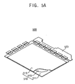
- FIG. 5A is a perspective view illustrating an exemplary display apparatus in accordance with exemplary embodiments of the present invention.
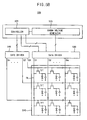
- FIG. 5B is a block diagram illustrating an exemplary display apparatus in accordance with exemplary embodiments of the present invention.
- the PCB shown in FIGS. 5A and 5B is substantially the same as or similar to the PCB illustrated in and described with respect to FIGS. 2 to 4 . Thus, any repetitive explanation concerning the PCB will be omitted.
- a display apparatus 500 includes a display panel 510 and a PCB 520.
- the display panel 510 includes a first substrate 511, a second substrate 513 and a liquid crystal layer 515.
- the first substrate 511 may include a plurality of gate lines G 1 , ..., G n (n is a positive integer greater than 1) and a plurality of data lines D 1 , ..., D m (m is a positive integer greater than 1).
- the data lines D 1 , ..., D m are electrically insulated from the gate lines G1, ..., G n and cross the gate lines G 1 , ..., G n .
- the first substrate 511 may further include a plurality of pixels for displaying images.
- a switching element TFT such as a thin film transistor ("TFT"), and a pixel electrode (not illustrated) are formed in each of the pixels.
- the second substrate 513 may include a color filter layer (not shown) and a common electrode (not shown) formed on the color filter layer.
- the liquid crystal layer 515 is disposed between the first substrate 511 and the second substrate 513.
- the liquid crystal layer 515 includes liquid crystal molecules. The arrangement of the liquid crystal molecules is changed by an electric field generated between the pixel electrode of the first substrate 511 and the common electrode of the second substrate 513, so that an amount of light passing through the liquid crystal layer 515 may be controlled.
- the display apparatus 500 may further include a gate driver 540 and a data driver 530.
- the gate driver 540 is controlled by the controller 521 to apply a gate driving signal to the gate lines G 1 , ..., G n .
- the data driver 530 is controlled by the controller 521 to apply an image signal to the data lines D 1 , ..., Dm.
- the data driver 530 applies the image signal to the data lines D 1 , ..., D m in response to output signals from the controller 521 and the gamma voltage generator 523.
- the image signal applied to the data lines D 1 , ..., D m is applied to the pixel electrode via the switching element TFT when the switching element TFT is turned on.
- the switching element TFT is turned on when the gate signal is applied to the gate lines G 1 , ..., G n .
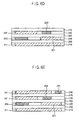
- FIGS. 6A to 6E are cross-sectional views illustrating an exemplary method of manufacturing an exemplary PCB in accordance with exemplary embodiments of the present invention.
- a first pattern structure 210 is formed on a lower surface of a first insulation substrate 250 and a second pattern structure 220 is formed on an upper surface of the first insulation substrate 250 opposite to the lower surface.
- the first pattern structure 210 includes a first ground pattern 211.
- the second pattern structure 220 includes a first line pattern 223 and a second ground pattern 221.
- the first line pattern 223 is formed above the first ground pattern 211, so as to overlap with the first ground pattern 211.
- the second ground pattern 221 is electrically insulated from the first line pattern 223, such as by being spaced and separated from the first line pattern 223.
- the first insulation substrate 250 electrically insulates the first pattern structure 210 and second pattern structure 220 from each other.
- a second insulation substrate 260 is disposed on the second pattern structure 220, such that a lower surface of the second insulation substrate 260 faces the second pattern structure 220.
- a third pattern structure 230 is formed on an upper surface of the second insulation substrate 260, where the upper surface is opposite to the lower surface of the second insulation substrate 260.
- the third pattern structure 230 includes a second line pattern 233 and a third ground pattern 231.
- the second line pattern 233 overlaps with the second ground pattern 221.
- the third ground pattern 231 is electrically insulated from the second line pattern 233, such as by being spaced and separated from the second line pattern 233, and overlaps with the first line pattern 223.
- the second insulation substrate 260 electrically insulates the second pattern structure 220 and the third pattern structure 230 from each other.
- a third insulation substrate 270 is disposed on the third pattern structure 230, such that a lower surface of the third insulation substrate 270 faces the third pattern structure 230.
- a fourth pattern structure 240 is formed on an upper surface of the third insulation substrate 270, where the upper surface is opposite to the lower surface of the third insulation substrate 270.
- the fourth pattern structure 240 includes a fourth ground pattern 241 and may further include a third line pattern 243.
- the fourth ground pattern 241 covers the second line pattern 233, such as by overlapping with the second line pattern 233.
- the third insulation substrate 270 electrically insulates the third pattern structure 230 and the fourth pattern structure 240 from each other. If provided, the third line pattern 243 overlaps an area of the third pattern structure 230 where the second line pattern 233 is not formed.
- a fourth insulation substrate may be formed on the fourth pattern structure 240.
- the first to fourth insulation substrates 250, 260, 270 may also be termed insulation layers.
- a controller may be further formed on one of the first to fourth insulation substrates 250, 260, 270.
- the controller may be electrically connected to the first line pattern 223 and the second line pattern 233.
- An original image signal provided by an external graphic device (not illustrated) is transferred from the external graphic device to the controller through the first line pattern 223.
- the controller generates an image signal and a control signal in response to the original image signal.
- the image signal and the control signal generated from the controller are transferred from the controller to a display panel through the second line pattern 233.
- the fourth pattern structure 240 may further include the third line pattern 243.
- a gamma voltage generator (not illustrated) may be further formed on one of the first to fourth insulation substrates 250, 260, 270. The gamma voltage generator may be electrically connected to the third line pattern 243.
- the third line pattern 243 may be separated from the second line pattern 233, so that the electromagnetic fields around the second line pattern 233 and the third line pattern 243 may not interfere with each other.
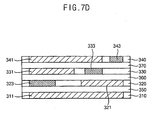
- FIGS. 7A to 7D are cross-sectional views illustrating an exemplary method of manufacturing an exemplary PCB in accordance with exemplary embodiments of the present invention.
- a first pattern structure 310 is formed on a lower surface of the first insulation substrate 350 and a second pattern structure 320 is formed on an upper surface of the first insulation substrate 350 opposite to the lower surface.
- the first pattern structure 310 includes a first ground pattern 311.
- the second pattern structure 320 includes a first line pattern 323 and the second ground pattern 321.
- the first line pattern 323 is formed above the first ground pattern 311, so as to overlap with the first ground pattern 311.
- the second ground pattern 321 is electrically insulated from the first line pattern 323, such as being spaced and separated from the first line pattern 323.
- a third pattern structure 330 is formed on a second insulation substrate 360.
- the third pattern structure 330 includes a second line pattern 333 and a third ground pattern 331.
- a fourth pattern structure 340 is formed on a third insulation substrate 370.
- the fourth pattern structure 340 includes a fourth ground pattern 341.
- the fourth pattern structure 340 may further include a third line pattern 343.
- the second insulation substrate 360 having the second line pattern 333 and the third ground pattern 331 formed thereon is disposed on the second pattern structure 320, so that the second line pattern 333 and the third ground pattern 331 are respectively located above the second ground pattern 321 and the first line pattern 323.
- the third insulation substrate 370 having the fourth ground pattern 341 formed thereon is disposed on the third pattern structure 330, so that the fourth ground pattern 341 is disposed above the second line pattern 333.
- the fourth pattern structure 340 includes the third line pattern 343, the third line pattern 343 is arranged such that it does not overlap with the second line pattern 333.
- signal line patterns are formed in inner pattern structures of the PCB between outermost pattern structures of the PCB and ground patterns are formed on and under the signal line patterns. Therefore, noise generated by EMI may be prevented.
- output line patterns of a controller may not overlap with gamma line patterns so that the noise may be further prevented.
Landscapes
- Engineering & Computer Science (AREA)
- Microelectronics & Electronic Packaging (AREA)
- Physics & Mathematics (AREA)
- Electromagnetism (AREA)
- Chemical & Material Sciences (AREA)
- Crystallography & Structural Chemistry (AREA)
- Computer Hardware Design (AREA)
- General Physics & Mathematics (AREA)
- Theoretical Computer Science (AREA)
- Devices For Indicating Variable Information By Combining Individual Elements (AREA)
- Structure Of Printed Boards (AREA)
- Shielding Devices Or Components To Electric Or Magnetic Fields (AREA)
- Production Of Multi-Layered Print Wiring Board (AREA)
Applications Claiming Priority (1)
| Application Number | Priority Date | Filing Date | Title |
|---|---|---|---|
| KR1020070091958A KR101385094B1 (ko) | 2007-09-11 | 2007-09-11 | 인쇄회로기판, 이를 갖는 표시장치 및 이의 제조방법 |
Publications (3)
| Publication Number | Publication Date |
|---|---|
| EP2037722A2 EP2037722A2 (en) | 2009-03-18 |
| EP2037722A3 EP2037722A3 (en) | 2010-01-27 |
| EP2037722B1 true EP2037722B1 (en) | 2012-03-21 |
Family
ID=39863119
Family Applications (1)
| Application Number | Title | Priority Date | Filing Date |
|---|---|---|---|
| EP08006205A Active EP2037722B1 (en) | 2007-09-11 | 2008-03-29 | Printed circuit board, display apparatus having a printed circuit board and method of manufacturing the printed circuit board |
Country Status (5)
| Country | Link |
|---|---|
| US (3) | US8254136B2 (https=) |
| EP (1) | EP2037722B1 (https=) |
| JP (1) | JP5514419B2 (https=) |
| KR (1) | KR101385094B1 (https=) |
| CN (1) | CN101448361B (https=) |
Families Citing this family (9)
| Publication number | Priority date | Publication date | Assignee | Title |
|---|---|---|---|---|
| JP2011239040A (ja) * | 2010-05-06 | 2011-11-24 | Canon Inc | 撮像装置 |
| DE102011113656A1 (de) * | 2011-09-19 | 2013-03-21 | Erni Electronics Gmbh | Mehrlagige elektrische Leiterplatte |
| KR20160066649A (ko) * | 2014-12-02 | 2016-06-13 | 삼성디스플레이 주식회사 | 인쇄회로기판 및 이를 포함하는 표시장치 |
| KR102317897B1 (ko) | 2015-06-04 | 2021-10-28 | 삼성디스플레이 주식회사 | 테스트 보드 및 그의 구동방법 |
| GB2540792A (en) * | 2015-07-28 | 2017-02-01 | Airbus Operations Ltd | Vehicle fairing including an electrical routing |
| CN209329126U (zh) * | 2016-05-17 | 2019-08-30 | 株式会社村田制作所 | 传输线路基板及电子设备 |
| CN107831610A (zh) | 2017-10-26 | 2018-03-23 | 惠科股份有限公司 | 信号传输装置及显示装置 |
| US11670435B2 (en) | 2021-04-09 | 2023-06-06 | Apple Inc. | Hybrid cabling solution for higher bandwidth and millimeter wave applications |
| KR20240127729A (ko) * | 2023-02-16 | 2024-08-23 | 삼성전자주식회사 | 전자 장치 및 전자 장치의 동작 방법 |
Family Cites Families (40)
| Publication number | Priority date | Publication date | Assignee | Title |
|---|---|---|---|---|
| JPS6156493A (ja) * | 1984-08-28 | 1986-03-22 | 日本電気株式会社 | 多層回路基板の電源配線構造 |
| US5003273A (en) * | 1989-12-04 | 1991-03-26 | Itt Corporation | Multilayer printed circuit board with pseudo-coaxial transmission lines |
| US5165055A (en) * | 1991-06-28 | 1992-11-17 | Digital Equipment Corporation | Method and apparatus for a PCB and I/O integrated electromagnetic containment |
| EP0867942B1 (en) * | 1992-09-08 | 2002-04-24 | Seiko Epson Corporation | Liquid crystal display apparatus |
| US5376759A (en) * | 1993-06-24 | 1994-12-27 | Northern Telecom Limited | Multiple layer printed circuit board |
| JP3113153B2 (ja) * | 1994-07-26 | 2000-11-27 | 株式会社東芝 | 多層配線構造の半導体装置 |
| JPH1041637A (ja) * | 1996-07-23 | 1998-02-13 | Nec Corp | 高密度多層配線基板 |
| JP2867985B2 (ja) * | 1996-12-20 | 1999-03-10 | 日本電気株式会社 | プリント回路基板 |
| US6246112B1 (en) * | 1998-06-11 | 2001-06-12 | Intel Corporation | Interleaved signal trace routing |
| KR100293982B1 (ko) | 1998-08-03 | 2001-07-12 | 윤종용 | 액정패널 |
| KR100339019B1 (ko) | 1999-05-31 | 2002-05-31 | 윤종용 | 차동 신호 배선 방법 및 차동 신호 배선을 갖는 인쇄회로기판이 실장된 액정 표시 장치 |
| JP3669219B2 (ja) * | 1999-08-10 | 2005-07-06 | 日本電気株式会社 | 多層プリント配線板 |
| JP3267274B2 (ja) * | 1999-08-13 | 2002-03-18 | 日本電気株式会社 | 多層プリント基板 |
| TW507476B (en) * | 1999-11-09 | 2002-10-21 | Gul Technologies Singapore Ltd | Printed circuit boards with in-board shielded circuitry and method of producing the same |
| JP2001144451A (ja) * | 1999-11-12 | 2001-05-25 | Ibi Tech Co Ltd | 積層配線板 |
| JP3542028B2 (ja) | 2000-08-01 | 2004-07-14 | インターナショナル・ビジネス・マシーンズ・コーポレーション | Emi対策を施した回路基板 |
| US6614325B1 (en) * | 2000-08-31 | 2003-09-02 | Northrop Grumman Corporation | RF/IF signal distribution network utilizing broadside coupled stripline |
| JP3877132B2 (ja) * | 2000-11-20 | 2007-02-07 | 富士通株式会社 | 多層配線基板及び半導体装置 |
| CN1316858C (zh) * | 2001-04-27 | 2007-05-16 | 日本电气株式会社 | 高频电路基板及其制造方法 |
| US6420778B1 (en) * | 2001-06-01 | 2002-07-16 | Aralight, Inc. | Differential electrical transmission line structures employing crosstalk compensation and related methods |
| JP4834937B2 (ja) * | 2001-08-22 | 2011-12-14 | 凸版印刷株式会社 | 高周波回路用多層配線板 |
| US6555745B1 (en) * | 2001-10-19 | 2003-04-29 | Medtronic, Inc. | Electrical interconnect between an articulating display and a PC based planar board |
| JP4114353B2 (ja) * | 2002-01-16 | 2008-07-09 | 凸版印刷株式会社 | クロストークノイズ低減多層配線回路基板及びその製造方法 |
| JP2003289184A (ja) | 2002-03-28 | 2003-10-10 | Canon Inc | 多層プリント配線板 |
| JP2003309378A (ja) * | 2002-04-18 | 2003-10-31 | Mitsubishi Electric Corp | 信号伝送用多層配線板 |
| TW587322B (en) * | 2002-12-31 | 2004-05-11 | Phoenix Prec Technology Corp | Substrate with stacked via and fine circuit thereon, and method for fabricating the same |
| US7129416B1 (en) * | 2004-02-05 | 2006-10-31 | Apple Computer, Inc. | Hybrid ground grid for printed circuit board |
| US7294791B2 (en) * | 2004-09-29 | 2007-11-13 | Endicott Interconnect Technologies, Inc. | Circuitized substrate with improved impedance control circuitry, method of making same, electrical assembly and information handling system utilizing same |
| KR100598118B1 (ko) * | 2005-01-12 | 2006-07-10 | 삼성전자주식회사 | 적층형 인쇄회로기판 |
| US7268645B2 (en) * | 2005-05-09 | 2007-09-11 | Seiko Epson Corporation | Integrated resonator structure and methods for its manufacture and use |
| KR101256965B1 (ko) * | 2005-06-22 | 2013-04-26 | 엘지디스플레이 주식회사 | 액정표시장치 및 그 구동방법 |
| KR101192781B1 (ko) * | 2005-09-30 | 2012-10-18 | 엘지디스플레이 주식회사 | 액정표시장치의 구동회로 및 이의 구동방법 |
| KR100881303B1 (ko) * | 2005-11-02 | 2009-02-03 | 이비덴 가부시키가이샤 | 반도체 장치용 다층 프린트 배선판 및 그 제조 방법 |
| JP4808468B2 (ja) * | 2005-11-04 | 2011-11-02 | 日本メクトロン株式会社 | 混成多層回路基板およびその製造方法 |
| KR100768047B1 (ko) * | 2005-11-30 | 2007-10-18 | 엘지.필립스 엘시디 주식회사 | 유기발광다이오드 표시소자 및 그의 구동 방법 |
| US20070222052A1 (en) * | 2006-03-24 | 2007-09-27 | Kyocera Corporation | Wiring structure, multilayer wiring board, and electronic device |
| US8134084B2 (en) * | 2006-06-30 | 2012-03-13 | Shin-Etsu Polymer Co., Ltd. | Noise-suppressing wiring-member and printed wiring board |
| US8253721B2 (en) * | 2006-11-28 | 2012-08-28 | Lg Display Co., Ltd. | Liquid crystal display device including source voltage generator and method of driving liquid crystal display device |
| JP5444619B2 (ja) * | 2008-02-07 | 2014-03-19 | 株式会社ジェイテクト | 多層回路基板およびモータ駆動回路基板 |
| FR2966692B1 (fr) * | 2010-10-26 | 2012-12-14 | Sagem Defense Securite | Carte electronique, dispositif electronique comportant une telle carte et procede de protection d'une carte electronique |
-
2007
- 2007-09-11 KR KR1020070091958A patent/KR101385094B1/ko active Active
-
2008
- 2008-03-29 EP EP08006205A patent/EP2037722B1/en active Active
- 2008-09-04 US US12/204,015 patent/US8254136B2/en active Active
- 2008-09-11 CN CN2008101769735A patent/CN101448361B/zh active Active
- 2008-09-11 JP JP2008233077A patent/JP5514419B2/ja active Active
-
2012
- 2012-07-24 US US13/556,274 patent/US20120285009A1/en not_active Abandoned
-
2016
- 2016-10-18 US US15/296,434 patent/US9930770B2/en active Active
Also Published As
| Publication number | Publication date |
|---|---|
| US20170042020A1 (en) | 2017-02-09 |
| KR20090026893A (ko) | 2009-03-16 |
| JP2009071311A (ja) | 2009-04-02 |
| JP5514419B2 (ja) | 2014-06-04 |
| US9930770B2 (en) | 2018-03-27 |
| CN101448361B (zh) | 2013-08-07 |
| CN101448361A (zh) | 2009-06-03 |
| KR101385094B1 (ko) | 2014-04-14 |
| US20120285009A1 (en) | 2012-11-15 |
| US8254136B2 (en) | 2012-08-28 |
| EP2037722A3 (en) | 2010-01-27 |
| EP2037722A2 (en) | 2009-03-18 |
| US20090066624A1 (en) | 2009-03-12 |
Similar Documents
| Publication | Publication Date | Title |
|---|---|---|
| US9930770B2 (en) | Printed circuit board, display apparatus having a printed circuit board and method of manufacturing the printed circuit board | |
| US6710839B2 (en) | Display device | |
| JP3539555B2 (ja) | 液晶表示装置 | |
| JP6907276B2 (ja) | 超高解像度の液晶表示装置 | |
| US20070002243A1 (en) | Display substrate, display device having the same, and method thereof | |
| TW200417800A (en) | Liquid crystal display device | |
| KR20000057871A (ko) | 액정 표시 장치 | |
| CN108279804B (zh) | 显示面板和显示装置 | |
| US7453542B2 (en) | Display device having first and second offsetting transfer-connections connected between driving electrodes and wiring lines and bent respectively in different directions to adjust wiring line resistances | |
| US10847109B2 (en) | Active matrix substrate and display panel | |
| KR100531388B1 (ko) | 표시 장치 | |
| US7460203B2 (en) | Liquid crystal display device | |
| US20140176889A1 (en) | Liquid Crystal Display Device | |
| US8743305B2 (en) | Liquid crystal display device utilizing storage capacitor lines | |
| EP1426914B1 (en) | Electro-optical display device and method of manufacturing it | |
| US11550194B2 (en) | Active matrix substrate and display panel | |
| KR100990315B1 (ko) | 액정표시장치 | |
| KR100983753B1 (ko) | 액정표시장치 | |
| KR101537677B1 (ko) | 횡전계모드 액정표시소자 | |
| KR20090060053A (ko) | 액정표시장치 |
Legal Events
| Date | Code | Title | Description |
|---|---|---|---|
| PUAI | Public reference made under article 153(3) epc to a published international application that has entered the european phase |
Free format text: ORIGINAL CODE: 0009012 |
|
| AK | Designated contracting states |
Kind code of ref document: A2 Designated state(s): AT BE BG CH CY CZ DE DK EE ES FI FR GB GR HR HU IE IS IT LI LT LU LV MC MT NL NO PL PT RO SE SI SK TR |
|
| AX | Request for extension of the european patent |
Extension state: AL BA MK RS |
|
| PUAL | Search report despatched |
Free format text: ORIGINAL CODE: 0009013 |
|
| AK | Designated contracting states |
Kind code of ref document: A3 Designated state(s): AT BE BG CH CY CZ DE DK EE ES FI FR GB GR HR HU IE IS IT LI LT LU LV MC MT NL NO PL PT RO SE SI SK TR |
|
| AX | Request for extension of the european patent |
Extension state: AL BA MK RS |
|
| 17P | Request for examination filed |
Effective date: 20100630 |
|
| 17Q | First examination report despatched |
Effective date: 20100728 |
|
| AKX | Designation fees paid |
Designated state(s): DE FR GB NL |
|
| GRAP | Despatch of communication of intention to grant a patent |
Free format text: ORIGINAL CODE: EPIDOSNIGR1 |
|
| RAP1 | Party data changed (applicant data changed or rights of an application transferred) |
Owner name: SAMSUNG ELECTRONICS CO., LTD. |
|
| RIN1 | Information on inventor provided before grant (corrected) |
Inventor name: MYEONG, JI-MAN Inventor name: KIM, KWAN-HO Inventor name: JANG, ICK-KYU |
|
| GRAS | Grant fee paid |
Free format text: ORIGINAL CODE: EPIDOSNIGR3 |
|
| GRAA | (expected) grant |
Free format text: ORIGINAL CODE: 0009210 |
|
| AK | Designated contracting states |
Kind code of ref document: B1 Designated state(s): DE FR GB NL |
|
| REG | Reference to a national code |
Ref country code: GB Ref legal event code: FG4D |
|
| REG | Reference to a national code |
Ref country code: NL Ref legal event code: T3 |
|
| REG | Reference to a national code |
Ref country code: DE Ref legal event code: R096 Ref document number: 602008014203 Country of ref document: DE Effective date: 20120524 |
|
| RAP2 | Party data changed (patent owner data changed or rights of a patent transferred) |
Owner name: SAMSUNG ELECTRONICS CO., LTD. |
|
| REG | Reference to a national code |
Ref country code: NL Ref legal event code: SD Effective date: 20121017 |
|
| RAP2 | Party data changed (patent owner data changed or rights of a patent transferred) |
Owner name: SAMSUNG DISPLAY CO., LTD. |
|
| PLBE | No opposition filed within time limit |
Free format text: ORIGINAL CODE: 0009261 |
|
| STAA | Information on the status of an ep patent application or granted ep patent |
Free format text: STATUS: NO OPPOSITION FILED WITHIN TIME LIMIT |
|
| 26N | No opposition filed |
Effective date: 20130102 |
|
| REG | Reference to a national code |
Ref country code: FR Ref legal event code: TP Owner name: SAMSUNG DISPLAY CO. LTD, KR Effective date: 20130226 |
|
| REG | Reference to a national code |
Ref country code: GB Ref legal event code: 732E Free format text: REGISTERED BETWEEN 20130307 AND 20130313 |
|
| REG | Reference to a national code |
Ref country code: DE Ref legal event code: R097 Ref document number: 602008014203 Country of ref document: DE Effective date: 20130102 |
|
| REG | Reference to a national code |
Ref country code: DE Ref legal event code: R082 Ref document number: 602008014203 Country of ref document: DE Representative=s name: DR. WEITZEL & PARTNER, DE |
|
| REG | Reference to a national code |
Ref country code: DE Ref legal event code: R082 Ref document number: 602008014203 Country of ref document: DE Representative=s name: DR. WEITZEL & PARTNER, DE Effective date: 20130422 Ref country code: DE Ref legal event code: R081 Ref document number: 602008014203 Country of ref document: DE Owner name: SAMSUNG DISPLAY CO., LTD., KR Free format text: FORMER OWNER: SAMSUNG ELECTRONICS CO., LTD, SUWON-SI, GYEONGGI-DO, KR Effective date: 20130422 Ref country code: DE Ref legal event code: R081 Ref document number: 602008014203 Country of ref document: DE Owner name: SAMSUNG DISPLAY CO., LTD., YONGIN-CITY, KR Free format text: FORMER OWNER: SAMSUNG ELECTRONICS CO., LTD, SUWON-SI, GYEONGGI-DO, KR Effective date: 20130422 Ref country code: DE Ref legal event code: R082 Ref document number: 602008014203 Country of ref document: DE Representative=s name: DR. WEITZEL & PARTNER PATENT- UND RECHTSANWAEL, DE Effective date: 20130422 |
|
| REG | Reference to a national code |
Ref country code: FR Ref legal event code: PLFP Year of fee payment: 9 |
|
| REG | Reference to a national code |
Ref country code: FR Ref legal event code: PLFP Year of fee payment: 10 |
|
| REG | Reference to a national code |
Ref country code: FR Ref legal event code: PLFP Year of fee payment: 11 |
|
| P01 | Opt-out of the competence of the unified patent court (upc) registered |
Effective date: 20230516 |
|
| PGFP | Annual fee paid to national office [announced via postgrant information from national office to epo] |
Ref country code: NL Payment date: 20260220 Year of fee payment: 19 |
|
| PGFP | Annual fee paid to national office [announced via postgrant information from national office to epo] |
Ref country code: GB Payment date: 20260224 Year of fee payment: 19 |
|
| PGFP | Annual fee paid to national office [announced via postgrant information from national office to epo] |
Ref country code: DE Payment date: 20260220 Year of fee payment: 19 |
|
| PGFP | Annual fee paid to national office [announced via postgrant information from national office to epo] |
Ref country code: FR Payment date: 20260224 Year of fee payment: 19 |