EP2014702B1 - Dispositif DEL contenant du polyborosiloxane - Google Patents
Dispositif DEL contenant du polyborosiloxane Download PDFInfo
- Publication number
- EP2014702B1 EP2014702B1 EP08012126A EP08012126A EP2014702B1 EP 2014702 B1 EP2014702 B1 EP 2014702B1 EP 08012126 A EP08012126 A EP 08012126A EP 08012126 A EP08012126 A EP 08012126A EP 2014702 B1 EP2014702 B1 EP 2014702B1
- Authority
- EP
- European Patent Office
- Prior art keywords
- group
- resin
- polyborosiloxane
- silicon compound
- independently represent
- Prior art date
- Legal status (The legal status is an assumption and is not a legal conclusion. Google has not performed a legal analysis and makes no representation as to the accuracy of the status listed.)
- Ceased
Links
- 229920005989 resin Polymers 0.000 claims description 46
- 239000011347 resin Substances 0.000 claims description 46
- 150000003377 silicon compounds Chemical class 0.000 claims description 33
- 125000000217 alkyl group Chemical group 0.000 claims description 22
- 238000005538 encapsulation Methods 0.000 claims description 21
- 239000004327 boric acid Substances 0.000 claims description 19
- 125000003118 aryl group Chemical group 0.000 claims description 17
- 230000003287 optical effect Effects 0.000 claims description 17
- 239000004065 semiconductor Substances 0.000 claims description 17
- 125000003545 alkoxy group Chemical group 0.000 claims description 12
- 230000001588 bifunctional effect Effects 0.000 claims description 10
- 150000001639 boron compounds Chemical class 0.000 claims description 10
- 125000005843 halogen group Chemical group 0.000 claims description 10
- 125000003342 alkenyl group Chemical group 0.000 claims description 9
- 125000000304 alkynyl group Chemical group 0.000 claims description 9
- 125000000753 cycloalkyl group Chemical group 0.000 claims description 9
- -1 boric acid compound Chemical class 0.000 claims description 8
- 125000002887 hydroxy group Chemical group [H]O* 0.000 claims description 8
- 125000004435 hydrogen atom Chemical group [H]* 0.000 claims description 3
- 229920000647 polyepoxide Polymers 0.000 description 13
- KGBXLFKZBHKPEV-UHFFFAOYSA-N boric acid Chemical compound OB(O)O KGBXLFKZBHKPEV-UHFFFAOYSA-N 0.000 description 12
- 239000003822 epoxy resin Substances 0.000 description 12
- 125000000524 functional group Chemical group 0.000 description 9
- 239000007788 liquid Substances 0.000 description 9
- 230000000052 comparative effect Effects 0.000 description 8
- 150000001875 compounds Chemical class 0.000 description 8
- 238000000862 absorption spectrum Methods 0.000 description 7
- 238000010438 heat treatment Methods 0.000 description 7
- 238000005259 measurement Methods 0.000 description 7
- 239000000758 substrate Substances 0.000 description 7
- ZWEHNKRNPOVVGH-UHFFFAOYSA-N 2-Butanone Chemical compound CCC(C)=O ZWEHNKRNPOVVGH-UHFFFAOYSA-N 0.000 description 6
- 239000006227 byproduct Substances 0.000 description 6
- 230000008020 evaporation Effects 0.000 description 6
- 238000001704 evaporation Methods 0.000 description 6
- 239000000463 material Substances 0.000 description 6
- 125000002496 methyl group Chemical group [H]C([H])([H])* 0.000 description 6
- OKTJSMMVPCPJKN-UHFFFAOYSA-N Carbon Chemical compound [C] OKTJSMMVPCPJKN-UHFFFAOYSA-N 0.000 description 5
- 229910052799 carbon Inorganic materials 0.000 description 5
- JJQZDUKDJDQPMQ-UHFFFAOYSA-N dimethoxy(dimethyl)silane Chemical compound CO[Si](C)(C)OC JJQZDUKDJDQPMQ-UHFFFAOYSA-N 0.000 description 5
- 230000014759 maintenance of location Effects 0.000 description 5
- 238000000034 method Methods 0.000 description 5
- 125000000956 methoxy group Chemical group [H]C([H])([H])O* 0.000 description 5
- 239000012299 nitrogen atmosphere Substances 0.000 description 5
- 125000001997 phenyl group Chemical group [H]C1=C([H])C([H])=C(*)C([H])=C1[H] 0.000 description 5
- 238000006243 chemical reaction Methods 0.000 description 4
- 229910052801 chlorine Inorganic materials 0.000 description 4
- 125000001309 chloro group Chemical group Cl* 0.000 description 4
- AHUXYBVKTIBBJW-UHFFFAOYSA-N dimethoxy(diphenyl)silane Chemical compound C=1C=CC=CC=1[Si](OC)(OC)C1=CC=CC=C1 AHUXYBVKTIBBJW-UHFFFAOYSA-N 0.000 description 4
- 125000001495 ethyl group Chemical group [H]C([H])([H])C([H])([H])* 0.000 description 4
- BFXIKLCIZHOAAZ-UHFFFAOYSA-N methyltrimethoxysilane Chemical compound CO[Si](C)(OC)OC BFXIKLCIZHOAAZ-UHFFFAOYSA-N 0.000 description 4
- 239000002994 raw material Substances 0.000 description 4
- 229920002050 silicone resin Polymers 0.000 description 4
- 239000000126 substance Substances 0.000 description 4
- 238000002834 transmittance Methods 0.000 description 4
- ZNOCGWVLWPVKAO-UHFFFAOYSA-N trimethoxy(phenyl)silane Chemical compound CO[Si](OC)(OC)C1=CC=CC=C1 ZNOCGWVLWPVKAO-UHFFFAOYSA-N 0.000 description 4
- 239000004593 Epoxy Substances 0.000 description 3
- 239000011248 coating agent Substances 0.000 description 3
- 238000000576 coating method Methods 0.000 description 3
- KUGSJJNCCNSRMM-UHFFFAOYSA-N ethoxyboronic acid Chemical compound CCOB(O)O KUGSJJNCCNSRMM-UHFFFAOYSA-N 0.000 description 3
- 125000001449 isopropyl group Chemical group [H]C([H])([H])C([H])(*)C([H])([H])[H] 0.000 description 3
- 239000004973 liquid crystal related substance Substances 0.000 description 3
- 239000000203 mixture Substances 0.000 description 3
- 229920001296 polysiloxane Polymers 0.000 description 3
- LXBGSDVWAMZHDD-UHFFFAOYSA-N 2-methyl-1h-imidazole Chemical compound CC1=NC=CN1 LXBGSDVWAMZHDD-UHFFFAOYSA-N 0.000 description 2
- WKBOTKDWSSQWDR-UHFFFAOYSA-N Bromine atom Chemical group [Br] WKBOTKDWSSQWDR-UHFFFAOYSA-N 0.000 description 2
- 239000003086 colorant Substances 0.000 description 2
- 230000006866 deterioration Effects 0.000 description 2
- BYLOHCRAPOSXLY-UHFFFAOYSA-N dichloro(diethyl)silane Chemical compound CC[Si](Cl)(Cl)CC BYLOHCRAPOSXLY-UHFFFAOYSA-N 0.000 description 2
- SURBAJYBTYLRMQ-UHFFFAOYSA-N dioxido(propan-2-yloxy)borane Chemical compound CC(C)OB([O-])[O-] SURBAJYBTYLRMQ-UHFFFAOYSA-N 0.000 description 2
- 238000005516 engineering process Methods 0.000 description 2
- LNEPOXFFQSENCJ-UHFFFAOYSA-N haloperidol Chemical compound C1CC(O)(C=2C=CC(Cl)=CC=2)CCN1CCCC(=O)C1=CC=C(F)C=C1 LNEPOXFFQSENCJ-UHFFFAOYSA-N 0.000 description 2
- 238000002156 mixing Methods 0.000 description 2
- 238000006068 polycondensation reaction Methods 0.000 description 2
- 125000001436 propyl group Chemical group [H]C([*])([H])C([H])([H])C([H])([H])[H] 0.000 description 2
- 239000002904 solvent Substances 0.000 description 2
- 125000003903 2-propenyl group Chemical group [H]C([*])([H])C([H])=C([H])[H] 0.000 description 1
- FKBMTBAXDISZGN-UHFFFAOYSA-N 5-methyl-3a,4,5,6,7,7a-hexahydro-2-benzofuran-1,3-dione Chemical compound C1C(C)CCC2C(=O)OC(=O)C12 FKBMTBAXDISZGN-UHFFFAOYSA-N 0.000 description 1
- ZOXJGFHDIHLPTG-UHFFFAOYSA-N Boron Chemical group [B] ZOXJGFHDIHLPTG-UHFFFAOYSA-N 0.000 description 1
- 238000005033 Fourier transform infrared spectroscopy Methods 0.000 description 1
- XUIMIQQOPSSXEZ-UHFFFAOYSA-N Silicon Chemical group [Si] XUIMIQQOPSSXEZ-UHFFFAOYSA-N 0.000 description 1
- 239000012790 adhesive layer Substances 0.000 description 1
- 125000002723 alicyclic group Chemical group 0.000 description 1
- 125000002877 alkyl aryl group Chemical group 0.000 description 1
- 239000012298 atmosphere Substances 0.000 description 1
- 230000015572 biosynthetic process Effects 0.000 description 1
- IISBACLAFKSPIT-UHFFFAOYSA-N bisphenol A Chemical group C=1C=C(O)C=CC=1C(C)(C)C1=CC=C(O)C=C1 IISBACLAFKSPIT-UHFFFAOYSA-N 0.000 description 1
- 239000007795 chemical reaction product Substances 0.000 description 1
- 239000011247 coating layer Substances 0.000 description 1
- 239000004020 conductor Substances 0.000 description 1
- 125000000113 cyclohexyl group Chemical group [H]C1([H])C([H])([H])C([H])([H])C([H])(*)C([H])([H])C1([H])[H] 0.000 description 1
- 125000001511 cyclopentyl group Chemical group [H]C1([H])C([H])([H])C([H])([H])C([H])(*)C1([H])[H] 0.000 description 1
- OSXYHAQZDCICNX-UHFFFAOYSA-N dichloro(diphenyl)silane Chemical compound C=1C=CC=CC=1[Si](Cl)(Cl)C1=CC=CC=C1 OSXYHAQZDCICNX-UHFFFAOYSA-N 0.000 description 1
- GSENNYNYEKCQGA-UHFFFAOYSA-N dichloro-di(propan-2-yl)silane Chemical compound CC(C)[Si](Cl)(Cl)C(C)C GSENNYNYEKCQGA-UHFFFAOYSA-N 0.000 description 1
- GNEPOXWQWFSSOU-UHFFFAOYSA-N dichloro-methyl-phenylsilane Chemical compound C[Si](Cl)(Cl)C1=CC=CC=C1 GNEPOXWQWFSSOU-UHFFFAOYSA-N 0.000 description 1
- ZMAPKOCENOWQRE-UHFFFAOYSA-N diethoxy(diethyl)silane Chemical compound CCO[Si](CC)(CC)OCC ZMAPKOCENOWQRE-UHFFFAOYSA-N 0.000 description 1
- ZZNQQQWFKKTOSD-UHFFFAOYSA-N diethoxy(diphenyl)silane Chemical compound C=1C=CC=CC=1[Si](OCC)(OCC)C1=CC=CC=C1 ZZNQQQWFKKTOSD-UHFFFAOYSA-N 0.000 description 1
- VVKJJEAEVBNODX-UHFFFAOYSA-N diethoxy-di(propan-2-yl)silane Chemical compound CCO[Si](C(C)C)(C(C)C)OCC VVKJJEAEVBNODX-UHFFFAOYSA-N 0.000 description 1
- MNFGEHQPOWJJBH-UHFFFAOYSA-N diethoxy-methyl-phenylsilane Chemical compound CCO[Si](C)(OCC)C1=CC=CC=C1 MNFGEHQPOWJJBH-UHFFFAOYSA-N 0.000 description 1
- VSYLGGHSEIWGJV-UHFFFAOYSA-N diethyl(dimethoxy)silane Chemical compound CC[Si](CC)(OC)OC VSYLGGHSEIWGJV-UHFFFAOYSA-N 0.000 description 1
- OLLFKUHHDPMQFR-UHFFFAOYSA-N dihydroxy(diphenyl)silane Chemical compound C=1C=CC=CC=1[Si](O)(O)C1=CC=CC=C1 OLLFKUHHDPMQFR-UHFFFAOYSA-N 0.000 description 1
- VHPUZTHRFWIGAW-UHFFFAOYSA-N dimethoxy-di(propan-2-yl)silane Chemical compound CO[Si](OC)(C(C)C)C(C)C VHPUZTHRFWIGAW-UHFFFAOYSA-N 0.000 description 1
- CVQVSVBUMVSJES-UHFFFAOYSA-N dimethoxy-methyl-phenylsilane Chemical compound CO[Si](C)(OC)C1=CC=CC=C1 CVQVSVBUMVSJES-UHFFFAOYSA-N 0.000 description 1
- LIKFHECYJZWXFJ-UHFFFAOYSA-N dimethyldichlorosilane Chemical compound C[Si](C)(Cl)Cl LIKFHECYJZWXFJ-UHFFFAOYSA-N 0.000 description 1
- YYLGKUPAFFKGRQ-UHFFFAOYSA-N dimethyldiethoxysilane Chemical compound CCO[Si](C)(C)OCC YYLGKUPAFFKGRQ-UHFFFAOYSA-N 0.000 description 1
- KPUWHANPEXNPJT-UHFFFAOYSA-N disiloxane Chemical class [SiH3]O[SiH3] KPUWHANPEXNPJT-UHFFFAOYSA-N 0.000 description 1
- 230000000694 effects Effects 0.000 description 1
- 230000007613 environmental effect Effects 0.000 description 1
- 125000001301 ethoxy group Chemical group [H]C([H])([H])C([H])([H])O* 0.000 description 1
- SBRXLTRZCJVAPH-UHFFFAOYSA-N ethyl(trimethoxy)silane Chemical compound CC[Si](OC)(OC)OC SBRXLTRZCJVAPH-UHFFFAOYSA-N 0.000 description 1
- 125000002534 ethynyl group Chemical group [H]C#C* 0.000 description 1
- 230000004907 flux Effects 0.000 description 1
- 239000011521 glass Substances 0.000 description 1
- 239000012210 heat-resistant fiber Substances 0.000 description 1
- 230000001771 impaired effect Effects 0.000 description 1
- 239000011261 inert gas Substances 0.000 description 1
- 239000011256 inorganic filler Substances 0.000 description 1
- 229910003475 inorganic filler Inorganic materials 0.000 description 1
- 239000005340 laminated glass Substances 0.000 description 1
- 239000010410 layer Substances 0.000 description 1
- MLSKXPOBNQFGHW-UHFFFAOYSA-N methoxy(dioxido)borane Chemical compound COB([O-])[O-] MLSKXPOBNQFGHW-UHFFFAOYSA-N 0.000 description 1
- 239000005055 methyl trichlorosilane Substances 0.000 description 1
- JLUFWMXJHAVVNN-UHFFFAOYSA-N methyltrichlorosilane Chemical compound C[Si](Cl)(Cl)Cl JLUFWMXJHAVVNN-UHFFFAOYSA-N 0.000 description 1
- 125000001624 naphthyl group Chemical group 0.000 description 1
- 125000002868 norbornyl group Chemical group C12(CCC(CC1)C2)* 0.000 description 1
- 230000002093 peripheral effect Effects 0.000 description 1
- 239000005054 phenyltrichlorosilane Substances 0.000 description 1
- 238000001782 photodegradation Methods 0.000 description 1
- 238000012643 polycondensation polymerization Methods 0.000 description 1
- 229920000728 polyester Polymers 0.000 description 1
- 229920006267 polyester film Polymers 0.000 description 1
- 238000002360 preparation method Methods 0.000 description 1
- 239000000047 product Substances 0.000 description 1
- 125000002568 propynyl group Chemical group [*]C#CC([H])([H])[H] 0.000 description 1
- 230000009257 reactivity Effects 0.000 description 1
- 239000011342 resin composition Substances 0.000 description 1
- 238000007789 sealing Methods 0.000 description 1
- 229910000077 silane Inorganic materials 0.000 description 1
- 229920002545 silicone oil Polymers 0.000 description 1
- 238000003786 synthesis reaction Methods 0.000 description 1
- 125000003944 tolyl group Chemical group 0.000 description 1
- ZOYFEXPFPVDYIS-UHFFFAOYSA-N trichloro(ethyl)silane Chemical compound CC[Si](Cl)(Cl)Cl ZOYFEXPFPVDYIS-UHFFFAOYSA-N 0.000 description 1
- ORVMIVQULIKXCP-UHFFFAOYSA-N trichloro(phenyl)silane Chemical compound Cl[Si](Cl)(Cl)C1=CC=CC=C1 ORVMIVQULIKXCP-UHFFFAOYSA-N 0.000 description 1
- GPWLZOISJZHVHX-UHFFFAOYSA-N trichloro(propan-2-yl)silane Chemical compound CC(C)[Si](Cl)(Cl)Cl GPWLZOISJZHVHX-UHFFFAOYSA-N 0.000 description 1
- CPUDPFPXCZDNGI-UHFFFAOYSA-N triethoxy(methyl)silane Chemical compound CCO[Si](C)(OCC)OCC CPUDPFPXCZDNGI-UHFFFAOYSA-N 0.000 description 1
- JCVQKRGIASEUKR-UHFFFAOYSA-N triethoxy(phenyl)silane Chemical compound CCO[Si](OCC)(OCC)C1=CC=CC=C1 JCVQKRGIASEUKR-UHFFFAOYSA-N 0.000 description 1
- LGROXJWYRXANBB-UHFFFAOYSA-N trimethoxy(propan-2-yl)silane Chemical compound CO[Si](OC)(OC)C(C)C LGROXJWYRXANBB-UHFFFAOYSA-N 0.000 description 1
- 125000000391 vinyl group Chemical group [H]C([*])=C([H])[H] 0.000 description 1
- 238000004383 yellowing Methods 0.000 description 1
Images
Classifications
-
- C—CHEMISTRY; METALLURGY
- C08—ORGANIC MACROMOLECULAR COMPOUNDS; THEIR PREPARATION OR CHEMICAL WORKING-UP; COMPOSITIONS BASED THEREON
- C08G—MACROMOLECULAR COMPOUNDS OBTAINED OTHERWISE THAN BY REACTIONS ONLY INVOLVING UNSATURATED CARBON-TO-CARBON BONDS
- C08G77/00—Macromolecular compounds obtained by reactions forming a linkage containing silicon with or without sulfur, nitrogen, oxygen or carbon in the main chain of the macromolecule
- C08G77/48—Macromolecular compounds obtained by reactions forming a linkage containing silicon with or without sulfur, nitrogen, oxygen or carbon in the main chain of the macromolecule in which at least two but not all the silicon atoms are connected by linkages other than oxygen atoms
- C08G77/56—Boron-containing linkages
-
- H—ELECTRICITY
- H01—ELECTRIC ELEMENTS
- H01L—SEMICONDUCTOR DEVICES NOT COVERED BY CLASS H10
- H01L23/00—Details of semiconductor or other solid state devices
- H01L23/28—Encapsulations, e.g. encapsulating layers, coatings, e.g. for protection
- H01L23/29—Encapsulations, e.g. encapsulating layers, coatings, e.g. for protection characterised by the material, e.g. carbon
- H01L23/293—Organic, e.g. plastic
- H01L23/296—Organo-silicon compounds
-
- H—ELECTRICITY
- H01—ELECTRIC ELEMENTS
- H01L—SEMICONDUCTOR DEVICES NOT COVERED BY CLASS H10
- H01L2924/00—Indexing scheme for arrangements or methods for connecting or disconnecting semiconductor or solid-state bodies as covered by H01L24/00
- H01L2924/0001—Technical content checked by a classifier
- H01L2924/0002—Not covered by any one of groups H01L24/00, H01L24/00 and H01L2224/00
-
- H—ELECTRICITY
- H01—ELECTRIC ELEMENTS
- H01L—SEMICONDUCTOR DEVICES NOT COVERED BY CLASS H10
- H01L33/00—Semiconductor devices having potential barriers specially adapted for light emission; Processes or apparatus specially adapted for the manufacture or treatment thereof or of parts thereof; Details thereof
- H01L33/48—Semiconductor devices having potential barriers specially adapted for light emission; Processes or apparatus specially adapted for the manufacture or treatment thereof or of parts thereof; Details thereof characterised by the semiconductor body packages
- H01L33/52—Encapsulations
- H01L33/56—Materials, e.g. epoxy or silicone resin
Definitions
- the present invention relates to a light-emitting diode device comprising an optical semiconductor element encapsulated with a resin for optical semiconductor element encapsulation.
- LED light-emitting diode
- an encapsulating material plays a role of sealing and protecting LED so that the performance of LED does not deteriorate.
- epoxy resins have been widely used as an encapsulating material and JP-A-2006-274249 reports that an epoxy resin composition containing a specific component is excellent in resistance against photodeterioration.
- a silicone resin there has been known a polyborosiloxane resin having a chemical structure where a part of silicon atoms in the silicone are replaced by boron atoms. Since the polyborosiloxane resin is excellent in heat resistance, it is used as an insulating coating film for electric wires which require heat resistance. JP-A-10-152561 reports that a polyborosiloxane having both of heat resistance and humidity resistance is obtained by a two-stage reaction of specific silicon compounds.
- an epoxy resin as an encapsulating material is not sufficient in heat resistance, there arises a problem of deterioration of the resin with the increasing use of larger electric current due to the increase in light-emitting efficiency and luminous flux of LED.
- the epoxy resin is changed into yellow due to heat generated in the LED chip, so that there arises a problem of decrease in emission luminance.
- blue or white LED is encapsulated, there arises a problem that exposure to short-wavelength light (e.g., light having a wavelength of 350 to 500 nm) having a large energy causes photodegradation and thus yellowing occurs more severely.
- a silicone resin is excellent in heat resistance but the synthesis is cumbersome and complicated and the raw materials themselves cost high, so that there arises a problem that a product cannot be supplied at a low cost.
- JP-A-08-268735 discloses a heat-resistant laminated glass comprising an intermediate adhesive layer of a polymetallosiloxane such as polyborosiloxane.
- the polymetallosiloxane is produced by mixing a silicone oil with a silane compound and a boric acid compound and heating the mixture in order to effect a condensation polymerization.
- JP-A-58-210976 discloses a resin composition for use in bonding metallic members, said composition being prepared by mixing a polyborosiloxane resin with a silicone resin and an inorganic filler in specific amounts.
- JP-A-09-134614 discloses a heat-resistant insulated wire comprising a conductor coated with a coating layer, said layer being made from a polyborosiloxane resin.
- JP-A-09-013278 discloses the use of a coating material comprising a polyborosiloxane resin for the preparation of heat-resistant fibers and heat-resistant insulated wires.
- the object of the present invention is to provide a light-emitting diode device comprising an optical semiconductor element encapsulated with a resin for optical semiconductor element encapsulation, said resin containing a polyborosiloxane excellent in all of heat resistance, transparency, and light resistance.
- a light-emitting diode device comprising an optical semiconductor element encapsulated with a resin for optical semiconductor element encapsulation, wherein the resin comprises a polyborosiloxane obtained by reacting a silicon compound with a boron compound, wherein the silicon compound is at least one of a bifunctional silicon compound represented by the following formula (I):
- the resin for optical semiconductor element encapsulation used in the invention exhibits an excellent advantage that it is excellent in all of heat resistance, transparency, and light resistance. Therefore, the optical semiconductor device encapsulated using the resin can achieve a longer operating life.
- the resin containing a polyborosiloxane used in the invention is suitably used as a material for encapsulating an optical semiconductor element in a backlight for a liquid crystal screen, a traffic signal, an outdoor large display, an advertising signboard, and the like.
- the resin for optical semiconductor element encapsulation contains a polyborosiloxane obtained by reacting a silicon compound with a boron compound.
- silicon compound at least one of specific bifunctional or trifunctional silicon compounds is used.
- the bifunctional silicon compound is a compound represented by the following formula (I):
- bifunctional silicon compound represented by the formula (I) there may be mentioned diphenyldimethoxysilane, dimethyldimethoxysilane, diphenyldihydroxysilane, dimethyldiethoxysilane, diphenyldiethoxysilane, diethyldimethoxysilane, diethyldiethoxysilane, diisopropyldimethoxysilane, diisopropyldiethoxysilane, methylphenyldimethoxysilane, methylphenyldiethoxysilane, dimethyldichlorosilane, diphenyldichlorosilane, diethyldichlorosilane, diisopropyldichlorosilane or, methylphenyldichlorosilane, and they may be used singly or as a combination of two or more thereof.
- dimethyldimethoxysilane in which R 1 and R 2 each are a methyl group and X 1 and X 2 each are a methoxy group
- diphenyldimethoxysilane in which R 1 and R 2 each are a phenyl group and X 1 and X 2 each are a methoxy group.
- the trifunctional silicon compound is a compound represented by the following formula (II):
- the trifunctional silicon compound represented by the formula (II) there may be mentioned phenyltrimethoxysilane, methyltrimethoxysilane, methyltrichlorosilane, phenyltrichlorosilane, phenyltriethoxysilane, methyltriethoxysilane, ethyltrimethoxysilane, ethyltrichlorosilane, isopropyltrimethoxysilane, or isopropyltrichlorosilane, and they may be used singly or as a combination of two or more thereof.
- methyltrimethoxysilane in which R 3 is a methyl group and X 3 , X 4 , and X 5 each are a methoxy group
- phenyltrimethoxysilane in which R 3 is a phenyl group and X 3 , X 4 , and X 5 each are a methoxy group
- the resin for encapsulation may contain a silicon compound other than the bifunctional silicon compound represented by the formula (I) and the trifunctional silicon compound represented by the formula (II) within a range where the advantage of the invention is not impaired.
- the total content of the bifunctional silicon compound represented by the formula (I) and the trifunctional silicon compound represented by the formula (II) in the silicon compounds subjected to the reaction is preferably 30% by weight or more, more preferably 50% by weight or more, and further preferably 60 to 100% by weight or more.
- the weight ratio (bifunctional silicon compound /trifunctional silicon compound) of the bifunctional silicon compound represented by the formula (I) to the trifunctional silicon compound represented by the formula (II) is preferably 20/1 to 1/10, and more preferably 5/1 to 1/2.
- the functional groups of R 1 and R 2 in the formula (I) and R 3 in the formula (II) preferably satisfies such a relationship that the molar ratio (alkyl group/aryl group) of the alkyl group to the aryl group is 100/0 to 5/95, and more preferably 100/0 to 15/85.
- the boron compound is a boric acid compound or a boric acid ester compound represented by the following formula (III): wherein Y 1 , Y 2 , and Y 3 each independently represent a hydrogen atom or an alkyl group.
- the carbon number of the alkyl group in the formula (III) is preferably 1 to 12, more preferably 1 to 6, and further preferably 1 to 3. Specific examples thereof include a methyl group, an ethyl group, a propyl group, and an isopropyl group. Of these, preferred are an ethyl group and an isopropyl group, and more preferred is an ethyl group.
- boric acid As the compound represented by the formula (III), there may be mentioned boric acid, methyl borate, ethyl borate, or isopropyl borate, and they may be used singly or as a combination of two or more thereof. Of these, preferred are boric acid, ethyl borate, and isopropyl borate, and more preferred are boric acid and ethyl borate.
- the polycondensation of the silicon compound with the boron compound can be carried out, for example, at a temperature of 60 to 200°C under an inert gas atmosphere and in the absence of a solvent.
- a plurality of the silicon compounds although the compounds may be subjected to the reaction at a time, since the reactivity varies depending on the functional groups of the compounds, each of the compounds can be separately subjected to the reaction.
- the total weight ratio (silicon compound/boron compound) of the silicon compound to the boron compound is preferably 500/1 to 1/1, more preferably 100/1 to 2/1, further preferably 20/1 to 2/1, and still further preferably 5/1 to 2/1.
- by-products may be removed by evaporation, for example, by heat treatment at 100 to 200°C for 1 to 12 hours and then at 200 to 300°C for 1 to 24 hours.
- the softening point of the resin used in the invention is preferably 50 to 300°C, more preferably 80 to 250°C from the viewpoint of moldability and processability.
- the softening point is measured in acccordance with the method described in the following Examples.
- the transparency (transmittance at 450 nm) of the resin used in the invention is preferably 90% or more and more preferably 95% or more from the viewpoint of improving light resistance.
- the transparency (transmittance at 450 nm) is measured in accordance with the method described in the following Examples.
- the thus obtained resin containing the polyborosiloxane is not only excellent in heat resistance but also excellent in transparency and light resistance, it can be suitably used as a resin for optical semiconductor element encapsulation in a backlight for a liquid crystal screen, a traffic signal, an outdoor large display, an advertising signboard, and the like.
- the optical semiconductor device of the invention includes the resin containing the polyborosiloxane excellent in heat resistance, transparency, and light resistance as a resin for optical semiconductor element encapsulation, it becomes possible to maintain the emission luminance in a high state for a long period of time without deterioration of the encapsulating resin and thus the device can be suitably used.
- the resin was measured in accordance with the direct ATR method using an FTIR apparatus (FTIR-470, manufactured by JASCO Corporation).
- the resin was slowly heated to 250°C on a hot plate, the state was visually observed, and a temperature where the resin was softened so as to show slight flowability was determined as a softening point.
- the resin was dissolved in methyl ethyl ketone and the solution was applied on a glass plate and dried at 150°C for 1 hour to form a film (film thickness: 50 ⁇ m).
- the resultant sample was subjected to the measurement of transmittance using a spectrophotometer (U-4100, manufactured by Hitachi High-Technologies Corporation).
- the solution was applied on a biaxially oriented polyester film (50 ⁇ m, manufactured by Mitsubishi Chemical Polyester) so as to achieve a thickness of 100 ⁇ m, and the whole was dried at 130°C for 2 minutes to obtain a sheet containing an epoxy resin. Thereafter, three pieces of sheets obtained in the same manner were thermally laminated at 100°C to obtain an epoxy sheet (epoxy resin A) having a thickness of 300 ⁇ m.
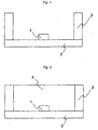
- FIG. 1 shows a substrate of the LED device before encapsulation processing
- FIG. 2 shows a substrate of the LED device after encapsulation processing.
- Each of LED devices of Examples 6 to 10 was produced by LED encapsulation in which a substrate mounted with a blue LED element having a size of 1 mm square and a reflector having a height of 400 ⁇ m sited around the LED element and 5 mm distant therefrom was heated to the encapsulating temperature shown in Table 1 and then 120 mg of the resin shown in Table 1 was put on the LED element and melted.
- An LED device of Comparative Example 1 was produced by LED encapsulation in which a substrate mounted with a blue LED element having a size of 1 mm square and a reflector having a height of 400 ⁇ m sited around the LED element and 5 mm distant therefrom was heated to the encapsulating temperature shown in Table 1 and then the resin shown in Table 1 was put on the LED element and subjected to encapsulation processing with a pressure of 0.5 MPa.
- Luminance retention was calculated according to the following equation to evaluate light resistance. In this connection, those having a luminance retention of 70% or more were judged to be good.
- Luminance Retention % Luminance after passage of 300 hours / Luminance immediately after start of test ⁇ 100 Table 1
- Example 6 Example 7
- Example 8 Example 9
- Example 10 Comparative Example 2 Resin Polyborosiloxane A (Example 1) Polyborosiloxane B (Example 2) Polyborosiloxane C (Example 3) Polyborosiloxane D (Example 4) Polyborosiloxane E (Example 5) Epoxy resin A (Comparative Example 1) Alkyl group/aryl group 1) 0/100 14/86 86/14 100/0 100/0 - Resin Softening point (°C) 80 100 200 250 250 impossible to measure 2) Transparency (%) 97 98 100 100 95 Heat resistance good good good good good good poor Encapsulation processing temperature 100 100 250 250 250 150 Device Luminance retention (%) 97 98 98 99 100 40 1) It shows a molar ratio (alkyl group/aryl group) of the alkyl group to the ary
- the LED devices of Examples have high luminance retention as compared with the LED device of Comparative Example and thus excellent in light resistance.
- the LED devices of Examples 8 to 10 have a molar ratio (alkyl group/aryl group) of the alkyl group to the aryl group of 86/14 or 100/0 with regard to the functional groups of the silicone compounds which are raw materials of the encapsulating resins, transparency and light resistance are more excellent.
Landscapes
- Chemical & Material Sciences (AREA)
- General Physics & Mathematics (AREA)
- Condensed Matter Physics & Semiconductors (AREA)
- Medicinal Chemistry (AREA)
- Polymers & Plastics (AREA)
- Engineering & Computer Science (AREA)
- Physics & Mathematics (AREA)
- Chemical Kinetics & Catalysis (AREA)
- Health & Medical Sciences (AREA)
- Organic Chemistry (AREA)
- Computer Hardware Design (AREA)
- Microelectronics & Electronic Packaging (AREA)
- Power Engineering (AREA)
- Led Device Packages (AREA)
- Structures Or Materials For Encapsulating Or Coating Semiconductor Devices Or Solid State Devices (AREA)
- Polymers With Sulfur, Phosphorus Or Metals In The Main Chain (AREA)
- Silicon Polymers (AREA)
Claims (1)
- Dispositif de diode électroluminescente comprenant un élément optique semi-conducteur encapsulé dans une résine d'encapsulation d'élément optique semi-conducteur, où ladite résine comprend un polyborosiloxane obtenu par réaction d'un composé du silicium avec un composé du bore,
le composé du silicium étant au moins l'un
d'un composé bifonctionnel du silicium représenté par la formule (I) ci-après : où R1 et R2 représentent chacun, indépendamment l'un de l'autre, un groupe alkyle, un groupe cycloalkyle, un groupe alcényle, un groupe alcynyle ou un groupe aryle, et X1 et X2 représentent chacun, indépendamment l'un de l'autre, un groupe alcoxy, un groupe hydroxyle ou un atome d'halogène ; etd'un composé trifonctionnel du silicium représenté par la formule (II) ci-après :
 où R3 représente un groupe alkyle, un groupe cycloalkyle, un groupe alcényle, un groupe alcynyle ou un groupe aryle, et X3, X4 et X5 représentent chacun, indépendamment les uns des autres, un groupe alcoxy, un groupe hydroxyle ou un atome d'halogène, etle composé du bore étant un composé acide borique ou un composé ester d'acide borique représenté par la formule (III) ci-après :
 où Y1, Y2 et Y3 représentent chacun, indépendamment les uns des autres, un atome d'hydrogène ou un groupe alkyle.
Applications Claiming Priority (1)
| Application Number | Priority Date | Filing Date | Title |
|---|---|---|---|
| JP2007182486A JP5024873B2 (ja) | 2007-07-11 | 2007-07-11 | ポリボロシロキサンからなる光半導体素子封止用樹脂 |
Publications (2)
| Publication Number | Publication Date |
|---|---|
| EP2014702A1 EP2014702A1 (fr) | 2009-01-14 |
| EP2014702B1 true EP2014702B1 (fr) | 2010-01-06 |
Family
ID=39708347
Family Applications (1)
| Application Number | Title | Priority Date | Filing Date |
|---|---|---|---|
| EP08012126A Ceased EP2014702B1 (fr) | 2007-07-11 | 2008-07-04 | Dispositif DEL contenant du polyborosiloxane |
Country Status (6)
| Country | Link |
|---|---|
| US (1) | US20090014750A1 (fr) |
| EP (1) | EP2014702B1 (fr) |
| JP (1) | JP5024873B2 (fr) |
| KR (1) | KR101153652B1 (fr) |
| CN (1) | CN101343367B (fr) |
| DE (1) | DE602008000500D1 (fr) |
Families Citing this family (17)
| Publication number | Priority date | Publication date | Assignee | Title |
|---|---|---|---|---|
| KR20090034953A (ko) * | 2006-08-04 | 2009-04-08 | 다우 코닝 코포레이션 | 실리콘 수지 및 실리콘 조성물 |
| JP5024878B2 (ja) * | 2007-11-28 | 2012-09-12 | 日東電工株式会社 | ポリボロシロキサンを含む光半導体素子封止用樹脂、およびそれを用いて得られる光半導体装置 |
| JP5084524B2 (ja) * | 2008-01-21 | 2012-11-28 | 日東電工株式会社 | 光半導体素子封止用樹脂組成物の製造方法 |
| US20110147722A1 (en) * | 2009-10-16 | 2011-06-23 | Hawker Craig J | Semiconductor light emitting device comprising high performance resins |
| TWI607786B (zh) | 2010-08-11 | 2017-12-11 | 極風有限責任公司 | 緩衝墊 |
| JP5655518B2 (ja) * | 2010-11-16 | 2015-01-21 | Jnc株式会社 | 新規物質及び熱硬化性組成物 |
| JP2012122002A (ja) * | 2010-12-09 | 2012-06-28 | Daicel Corp | 付加硬化性メタロシロキサン化合物 |
| EP2742085B1 (fr) | 2011-08-10 | 2021-12-01 | University of Virginia Patent Foundation | Compositions de caoutchouc silicone viscoélastiques |
| US9615611B2 (en) | 2011-08-11 | 2017-04-11 | G-Form, LLC | Breathable impact absorbing cushioning and constructions |
| CN103275325B (zh) * | 2013-06-09 | 2015-06-17 | 上海爱世博有机硅材料有限公司 | 硼硅氧烷及其制备方法 |
| CN106519242B (zh) * | 2016-11-23 | 2018-03-30 | 常州工程职业技术学院 | 一种紫外光固化钛掺杂含硼硅氧烷及其制备方法和在3d打印材料中的应用 |
| CN107312175A (zh) * | 2017-05-14 | 2017-11-03 | 杭州师范大学 | 一种线型聚硼硅氧烷的制备方法 |
| CN108913091A (zh) * | 2018-07-28 | 2018-11-30 | 南昌正业科技有限公司 | 一种柔性覆铜板用粘结剂及其制备方法 |
| CN109593509B (zh) * | 2018-12-06 | 2021-05-04 | 烟台德邦科技股份有限公司 | 一种硼酸改性有机硅热熔胶的制备方法 |
| CN111154453B (zh) * | 2020-01-19 | 2022-01-28 | 厦门艾贝森电子有限公司 | 一种耐热单组份加成型有机硅胶黏剂及其制备方法 |
| CN111394054A (zh) * | 2020-03-24 | 2020-07-10 | 新安天玉有机硅有限公司 | 一种自粘胶带用硅橡胶及其制备方法 |
| CN115044084B (zh) * | 2021-03-08 | 2023-10-03 | 四川大学 | 聚硼硅氧烷弹性体在显示屏保护中的应用 |
Family Cites Families (17)
| Publication number | Priority date | Publication date | Assignee | Title |
|---|---|---|---|---|
| US4152509A (en) * | 1976-09-30 | 1979-05-01 | The Foundation: The Research Institute For Special Inorganic Materials | Borosiloxane polymers and a method for producing the same |
| JPS53147798A (en) * | 1977-05-30 | 1978-12-22 | Shin Etsu Chem Co Ltd | Curable composition |
| JPS5483100A (en) * | 1977-12-14 | 1979-07-02 | Asahi Chem Ind Co Ltd | Borosiloxane polymer and its preparation |
| DK152779A (da) * | 1978-04-14 | 1979-10-15 | Castrol Ltd | Bor-siliciumforbindelser der er egnede til anvendelse i hydrauliske vaesker og fremgangsmaade til fremstilling deraf |
| JPS58210976A (ja) | 1982-06-02 | 1983-12-08 | Showa Electric Wire & Cable Co Ltd | 接着用樹脂組成物 |
| JPH04125929A (ja) * | 1990-09-17 | 1992-04-27 | Fujitsu Ltd | 半導体装置の絶縁膜形成方法および半導体装置 |
| JP3175124B2 (ja) * | 1991-11-14 | 2001-06-11 | 東亞合成株式会社 | シリカ系被覆材及び被覆体 |
| JPH08268735A (ja) | 1995-03-30 | 1996-10-15 | Central Glass Co Ltd | 耐熱性合せガラス |
| JPH0913278A (ja) | 1995-06-23 | 1997-01-14 | Showa Electric Wire & Cable Co Ltd | 耐熱繊維およびこれを用いた耐熱絶縁電線 |
| JPH09134614A (ja) | 1995-11-09 | 1997-05-20 | Showa Electric Wire & Cable Co Ltd | 耐熱性絶縁電線 |
| JPH10152561A (ja) * | 1996-11-26 | 1998-06-09 | Showa Electric Wire & Cable Co Ltd | ポリボロシロキサンの製造方法、ポリボロシロキサン塗膜及び該塗膜を有する無機絶縁電線 |
| JP4499907B2 (ja) * | 2000-12-07 | 2010-07-14 | 富士化学株式会社 | 無機高分子化合物の製造方法、無機高分子化合物、および無機高分子化合物膜 |
| JP4611617B2 (ja) * | 2002-04-26 | 2011-01-12 | 株式会社カネカ | 発光ダイオード |
| JP4634810B2 (ja) * | 2005-01-20 | 2011-02-16 | 信越化学工業株式会社 | シリコーン封止型led |
| TW200732382A (en) * | 2005-12-22 | 2007-09-01 | Rohm & Haas | Siloxane encapsulants |
| KR20090034953A (ko) * | 2006-08-04 | 2009-04-08 | 다우 코닝 코포레이션 | 실리콘 수지 및 실리콘 조성물 |
| JP2008231400A (ja) * | 2007-02-20 | 2008-10-02 | Suzuka Fuji Xerox Co Ltd | 光学素子用樹脂組成物及び硬化性樹脂組成物 |
-
2007
- 2007-07-11 JP JP2007182486A patent/JP5024873B2/ja not_active Expired - Fee Related
-
2008
- 2008-07-04 DE DE602008000500T patent/DE602008000500D1/de active Active
- 2008-07-04 EP EP08012126A patent/EP2014702B1/fr not_active Ceased
- 2008-07-11 CN CN200810135771.6A patent/CN101343367B/zh not_active Expired - Fee Related
- 2008-07-11 US US12/171,028 patent/US20090014750A1/en not_active Abandoned
- 2008-07-11 KR KR1020080067792A patent/KR101153652B1/ko not_active IP Right Cessation
Also Published As
| Publication number | Publication date |
|---|---|
| US20090014750A1 (en) | 2009-01-15 |
| JP2009019104A (ja) | 2009-01-29 |
| DE602008000500D1 (de) | 2010-02-25 |
| CN101343367B (zh) | 2012-04-11 |
| KR101153652B1 (ko) | 2012-06-18 |
| KR20090006804A (ko) | 2009-01-15 |
| JP5024873B2 (ja) | 2012-09-12 |
| CN101343367A (zh) | 2009-01-14 |
| EP2014702A1 (fr) | 2009-01-14 |
Similar Documents
| Publication | Publication Date | Title |
|---|---|---|
| EP2014702B1 (fr) | Dispositif DEL contenant du polyborosiloxane | |
| KR101836962B1 (ko) | 신규 유기 규소 화합물, 상기 유기 규소 화합물을 포함하는 열경화성 수지 조성물, 경화 수지 및 광 반도체용 봉지 재료 | |
| US8198380B2 (en) | Composition for thermosetting silicone resin | |
| JP4734832B2 (ja) | 光素子用封止材 | |
| EP1801163B1 (fr) | Encapsulants siloxane | |
| TWI421304B (zh) | 經聚矽氧烷樹脂組成物包覆的半導體裝置以及用於包覆半導體裝置之聚矽氧烷樹脂錠 | |
| JP5793824B2 (ja) | 有機ケイ素化合物、該有機ケイ素化合物を含む熱硬化性組成物、および光半導体用封止材料 | |
| KR20090055500A (ko) | 폴리알루미노실록산을 함유하는 광반도체-소자 밀봉용 수지및 이를 이용하여 얻어지는 광반도체 디바이스 | |
| US7985807B2 (en) | Thermosetting composition | |
| KR20160035581A (ko) | 발광다이오드를 위한 봉지재 | |
| KR101472829B1 (ko) | 경화성 조성물, 경화물, 광반도체 장치 및 폴리실록산 | |
| KR20140068780A (ko) | 발광 다이오드 | |
| Liu et al. | Self‐adhesive epoxy modified silicone materials for light emitting diode encapsulation | |
| WO2019163686A1 (fr) | Composé silicium organique liquide, et composition de résine thermodurcissable à laquelle celui-ci est mélangé | |
| KR20120078614A (ko) | 봉지재용 투광성 수지, 상기 투광성 수지를 포함하는 봉지재 및 전자 소자 | |
| US8153748B2 (en) | Thermosetting composition | |
| KR101464271B1 (ko) | 열경화성 실리콘 수지 조성물 및 이를 이용한 전자장치 | |
| KR20160148449A (ko) | 경화성 수지 조성물, 광학 소자 및 광반도체 장치 | |
| WO2014052937A1 (fr) | Composition de polysiloxane polycyclique et diode électroluminescente la contenant | |
| JP6766334B2 (ja) | 有機ケイ素化合物、該有機ケイ素化合物を含む熱硬化性組成物、および光半導体用封止材料 | |
| JP2020158692A (ja) | フッ素含有縮合型オルガノポリシロキサンプレポリマーおよびその硬化体 | |
| KR20160016417A (ko) | 화합물, 투광성 수지 조성물 및 봉지재 |
Legal Events
| Date | Code | Title | Description |
|---|---|---|---|
| PUAI | Public reference made under article 153(3) epc to a published international application that has entered the european phase |
Free format text: ORIGINAL CODE: 0009012 |
|
| AK | Designated contracting states |
Kind code of ref document: A1 Designated state(s): AT BE BG CH CY CZ DE DK EE ES FI FR GB GR HR HU IE IS IT LI LT LU LV MC MT NL NO PL PT RO SE SI SK TR |
|
| AX | Request for extension of the european patent |
Extension state: AL BA MK RS |
|
| 17P | Request for examination filed |
Effective date: 20090217 |
|
| 17Q | First examination report despatched |
Effective date: 20090316 |
|
| GRAP | Despatch of communication of intention to grant a patent |
Free format text: ORIGINAL CODE: EPIDOSNIGR1 |
|
| RTI1 | Title (correction) |
Free format text: LED DEVICE COMPRISING A POLYBOROSILOXANE |
|
| AKX | Designation fees paid |
Designated state(s): DE NL |
|
| GRAS | Grant fee paid |
Free format text: ORIGINAL CODE: EPIDOSNIGR3 |
|
| GRAA | (expected) grant |
Free format text: ORIGINAL CODE: 0009210 |
|
| AK | Designated contracting states |
Kind code of ref document: B1 Designated state(s): DE NL |
|
| REF | Corresponds to: |
Ref document number: 602008000500 Country of ref document: DE Date of ref document: 20100225 Kind code of ref document: P |
|
| REG | Reference to a national code |
Ref country code: NL Ref legal event code: T3 |
|
| PLBE | No opposition filed within time limit |
Free format text: ORIGINAL CODE: 0009261 |
|
| STAA | Information on the status of an ep patent application or granted ep patent |
Free format text: STATUS: NO OPPOSITION FILED WITHIN TIME LIMIT |
|
| 26N | No opposition filed |
Effective date: 20101007 |
|
| PGFP | Annual fee paid to national office [announced via postgrant information from national office to epo] |
Ref country code: DE Payment date: 20140702 Year of fee payment: 7 Ref country code: NL Payment date: 20140610 Year of fee payment: 7 |
|
| REG | Reference to a national code |
Ref country code: DE Ref legal event code: R119 Ref document number: 602008000500 Country of ref document: DE |
|
| REG | Reference to a national code |
Ref country code: NL Ref legal event code: MM Effective date: 20150801 |
|
| PG25 | Lapsed in a contracting state [announced via postgrant information from national office to epo] |
Ref country code: DE Free format text: LAPSE BECAUSE OF NON-PAYMENT OF DUE FEES Effective date: 20160202 |
|
| PG25 | Lapsed in a contracting state [announced via postgrant information from national office to epo] |
Ref country code: NL Free format text: LAPSE BECAUSE OF NON-PAYMENT OF DUE FEES Effective date: 20150801 |