EP2013908B1 - Halbleiter-leuchtdiode mit integrierten elektronischen bauteilen - Google Patents
Halbleiter-leuchtdiode mit integrierten elektronischen bauteilen Download PDFInfo
- Publication number
- EP2013908B1 EP2013908B1 EP07735517.0A EP07735517A EP2013908B1 EP 2013908 B1 EP2013908 B1 EP 2013908B1 EP 07735517 A EP07735517 A EP 07735517A EP 2013908 B1 EP2013908 B1 EP 2013908B1
- Authority
- EP
- European Patent Office
- Prior art keywords
- light emitting
- layer
- emitting device
- contact
- semiconductor light
- Prior art date
- Legal status (The legal status is an assumption and is not a legal conclusion. Google has not performed a legal analysis and makes no representation as to the accuracy of the status listed.)
- Active
Links
Images




Classifications
-
- H—ELECTRICITY
- H10—SEMICONDUCTOR DEVICES; ELECTRIC SOLID-STATE DEVICES NOT OTHERWISE PROVIDED FOR
- H10H—INORGANIC LIGHT-EMITTING SEMICONDUCTOR DEVICES HAVING POTENTIAL BARRIERS
- H10H29/00—Integrated devices, or assemblies of multiple devices, comprising at least one light-emitting semiconductor element covered by group H10H20/00
- H10H29/10—Integrated devices comprising at least one light-emitting semiconductor component covered by group H10H20/00
-
- H—ELECTRICITY
- H10—SEMICONDUCTOR DEVICES; ELECTRIC SOLID-STATE DEVICES NOT OTHERWISE PROVIDED FOR
- H10W—GENERIC PACKAGES, INTERCONNECTIONS, CONNECTORS OR OTHER CONSTRUCTIONAL DETAILS OF DEVICES COVERED BY CLASS H10
- H10W72/00—Interconnections or connectors in packages
- H10W72/50—Bond wires
- H10W72/551—Materials of bond wires
- H10W72/552—Materials of bond wires comprising metals or metalloids, e.g. silver
- H10W72/5522—Materials of bond wires comprising metals or metalloids, e.g. silver comprising gold [Au]
-
- H—ELECTRICITY
- H10—SEMICONDUCTOR DEVICES; ELECTRIC SOLID-STATE DEVICES NOT OTHERWISE PROVIDED FOR
- H10W—GENERIC PACKAGES, INTERCONNECTIONS, CONNECTORS OR OTHER CONSTRUCTIONAL DETAILS OF DEVICES COVERED BY CLASS H10
- H10W72/00—Interconnections or connectors in packages
- H10W72/851—Dispositions of multiple connectors or interconnections
- H10W72/874—On different surfaces
- H10W72/884—Die-attach connectors and bond wires
-
- H—ELECTRICITY
- H10—SEMICONDUCTOR DEVICES; ELECTRIC SOLID-STATE DEVICES NOT OTHERWISE PROVIDED FOR
- H10W—GENERIC PACKAGES, INTERCONNECTIONS, CONNECTORS OR OTHER CONSTRUCTIONAL DETAILS OF DEVICES COVERED BY CLASS H10
- H10W74/00—Encapsulations, e.g. protective coatings
- H10W74/10—Encapsulations, e.g. protective coatings characterised by their shape or disposition
- H10W74/15—Encapsulations, e.g. protective coatings characterised by their shape or disposition on active surfaces of flip-chip devices, e.g. underfills
-
- H—ELECTRICITY
- H10—SEMICONDUCTOR DEVICES; ELECTRIC SOLID-STATE DEVICES NOT OTHERWISE PROVIDED FOR
- H10W—GENERIC PACKAGES, INTERCONNECTIONS, CONNECTORS OR OTHER CONSTRUCTIONAL DETAILS OF DEVICES COVERED BY CLASS H10
- H10W90/00—Package configurations
- H10W90/701—Package configurations characterised by the relative positions of pads or connectors relative to package parts
- H10W90/721—Package configurations characterised by the relative positions of pads or connectors relative to package parts of bump connectors
- H10W90/722—Package configurations characterised by the relative positions of pads or connectors relative to package parts of bump connectors between stacked chips
-
- H—ELECTRICITY
- H10—SEMICONDUCTOR DEVICES; ELECTRIC SOLID-STATE DEVICES NOT OTHERWISE PROVIDED FOR
- H10W—GENERIC PACKAGES, INTERCONNECTIONS, CONNECTORS OR OTHER CONSTRUCTIONAL DETAILS OF DEVICES COVERED BY CLASS H10
- H10W90/00—Package configurations
- H10W90/701—Package configurations characterised by the relative positions of pads or connectors relative to package parts
- H10W90/731—Package configurations characterised by the relative positions of pads or connectors relative to package parts of die-attach connectors
- H10W90/732—Package configurations characterised by the relative positions of pads or connectors relative to package parts of die-attach connectors between stacked chips
-
- H—ELECTRICITY
- H10—SEMICONDUCTOR DEVICES; ELECTRIC SOLID-STATE DEVICES NOT OTHERWISE PROVIDED FOR
- H10W—GENERIC PACKAGES, INTERCONNECTIONS, CONNECTORS OR OTHER CONSTRUCTIONAL DETAILS OF DEVICES COVERED BY CLASS H10
- H10W90/00—Package configurations
- H10W90/701—Package configurations characterised by the relative positions of pads or connectors relative to package parts
- H10W90/731—Package configurations characterised by the relative positions of pads or connectors relative to package parts of die-attach connectors
- H10W90/736—Package configurations characterised by the relative positions of pads or connectors relative to package parts of die-attach connectors between a chip and a stacked lead frame, conducting package substrate or heat sink
-
- H—ELECTRICITY
- H10—SEMICONDUCTOR DEVICES; ELECTRIC SOLID-STATE DEVICES NOT OTHERWISE PROVIDED FOR
- H10W—GENERIC PACKAGES, INTERCONNECTIONS, CONNECTORS OR OTHER CONSTRUCTIONAL DETAILS OF DEVICES COVERED BY CLASS H10
- H10W90/00—Package configurations
- H10W90/701—Package configurations characterised by the relative positions of pads or connectors relative to package parts
- H10W90/751—Package configurations characterised by the relative positions of pads or connectors relative to package parts of bond wires
- H10W90/756—Package configurations characterised by the relative positions of pads or connectors relative to package parts of bond wires between a chip and a stacked lead frame, conducting package substrate or heat sink
Definitions
- the present invention relates to semiconductor light emitting devices including integrated electronic components.
- LEDs light emitting diodes
- RCLEDs resonant cavity light emitting diodes
- VCSELs vertical cavity laser diodes
- edge emitting lasers are among the most efficient light sources currently available.
- Materials systems currently of interest in the manufacture of high-brightness light emitting devices capable of operation across the visible spectrum include Group III-V semiconductors, particularly binary, ternary, and quaternary alloys of gallium, aluminum, indium, and nitrogen, also referred to as III-nitride materials.
- III-nitride light emitting devices are fabricated by epitaxially growing a stack of semiconductor layers of different compositions and dopant concentr on a sapphire, silicon carbide, III-nitride, or other suitable substrate by metal-organic chemical vapor deposition (MOCVD), molecular beam epitaxy (MBE), or other epitaxial techniques.
- MOCVD metal-organic chemical vapor deposition
- MBE molecular beam epitaxy
- the stack often includes one or more n-type layers doped with, for example, Si, formed over the substrate, a light emitting or active region formed over the n-type layer or layers, and one or more p-type layers doped with, for example, Mg, formed over the active region.
- III-nitride devices formed on conductive substrates may have the p- and n-contacts formed on opposite sides of the device.
- III-nitride devices are fabricated on insulating substrates, such as sapphire, with both contacts on the same side of the device. Such devices are mounted so light is extracted either through the contacts (known as an epitaxy-up device) or through a surface of the device opposite the contacts (known as a flip chip device).
- Fig. 1 illustrates a prior art III-nitride device mounted on a silicon diode element that includes an electrostatic discharge protection circuit, described in more detail in Fig. 13 and column 19 lines 29-64 of U.S. Patent 6,333,522 .
- GaN LED element 1 is mounted on leadframes 13a and 13b with a Si diode element 2 having p-side and n-side electrodes interposed there between, not directly on the leadframes.
- the Si diode element 2 with the main surface thereof facing upward and with the back face thereof facing downward is disposed on a die pad forming the tip of the lead frame 13a having a reflecting mirror.
- the Si diode element 2 is die-bonded to the die pad with an Ag paste 14, while having an n-side electrode 9 on the back face thereof in contact with the die pad of the lead frame 13a.
- a p-side electrode 7, an n-side electrode 8, and a bonding pad portion 10 of the p-side electrode are provided on the top face of the Si diode element 2.
- the GaN LED element 1 having the top face of the sapphire substrate facing downward and the p-side and n-side electrodes 5 and 6 facing downward is positioned above the Si diode element 2.
- the p-side and n-side electrodes 5 and 6 of the GaN LED element 1 are electrically connected to the n-side and p-side electrodes 8 and 7 of the Si diode element 2 via Au micro bump 12 and 11, respectively.
- the GaN LED element 1 is fixed to the Si diode element 2 with a UV curable insulating resin 16.
- the mechanical connection between the GaN LED element 1 and the Si diode element 2 may be accomplished by welding the micro bumps 11 and 12 instead of using the UV, curable insulating resin 16.
- the bonding pad portion 10 of the p-side electrode of the Si diode element 2 is connected by wire bonding to the lead frame 13b via an Au wire 17.
- a reflector 15 for upwardly reflecting light is attached to a side face of the die pad of the lead frame 13a, whereby the GaN LED element 1 is surrounded.
- the tip portions of the leadframes 13a and 13b are entirely molded with a transparent epoxy resin 18 with the GaN LED element 1 and the Si diode element 2 mounted thereon to constitute the LED lamp.
- circuit elements besides electrostatic discharge protection circuitry may be included in the silicon diode illustrated in Fig. 1 .
- One drawback to the device illustrated in Fig. 1 is the external silicon structure on which LED element 1 is mounted limits the flexibility of the design of the LED element and the package. Also, the external silicon structure may undesirably increase the source size of the light source provided by LED element 1, potentially complicating the design and increasing the cost of optics such as lenses used with the device shown in Fig. 1 .
- FIG. 17 is reproduced here as Fig. 2 , which illustrates a GaN LED element 1 with a double heterostructure comprising a GaN buffer layer 31, an n-type GaN layer 32, an InGaN active layer 33, a p-type AlGaN layer 34, and a p-type GaN layer 35 which are stacked sequentially in layers on the top face of a sapphire substrate 30.
- the top face of the n-type GaN layer 32 has a stepped configuration consisting of an upper-level portion occupying the major part of the top face and a lower-level portion occupying the remaining minor part thereof
- An n-side electrode 6 made of a Ti/Au multi-layer film and a Ni/Au multilayer film laminated thereon is formed in stacking relation on the top face of the lower-level portion of the n-type GaN layer 32.
- the aforesaid InGaN active layer 33, p-type AlGaN layer 34, and p-type GaN layer 35 are stacked sequentially in layers on the top face of the upper-level portion of the n-type GaN layer 32.
- a p-side electrode 5 made of Ni and Au is disposed directly on the top face of the p-type GaN layer 35 with no intervention of a transparent electrode for current diffusion. See U.S. Patent No. 6,333,522 , column 12 lines 22-40.
- An interlayer insulating film 51 made of a silicon oxide film is formed on the GaN LED element 1.
- a p-type semiconductor region 52 and an n-type semiconductor region 53 are formed.
- the silicon thin film can be formed easily by utilizing TFT formation technology associated with a liquid-crystal device.
- the diode element 50 is provided with a p-side electrode 54 filling in a through hole formed in the interlayer insulating film 51 to be connected to the n-side electrode 6 of the GaN LED element 1, while being connected to the p-type semiconductor region 52 thereof.
- the diode element 50 is also provided with an n-side electrode 55 filling in a though hole formed in the interlayer insulating film 51 to be connected to the p-side electrode 5 of the GaN LED element 1, while being connected to the n-type semiconductor region 53 thereof.
- the p-side and n-side electrodes 54 and 55 of the diode element 50 are connected to leadframes by wire bonding. In this case, light generated by the GaN LED element 1 is reflected by the leadframes and emitted upward.
- the diode element 50 can be formed in a narrow limited region, desired light-emitting efficiency can easily be achieved. See U.S. Patent No. 6,333,522 , column 23 lines 19-42.
- the small size of the electrostatic discharge protection diode in the device of Fig. 2 limits its ability to protect the LED element from electrostatic discharge.
- one or more circuit elements such as silicon diodes, resistors, capacitors, and inductors are disposed between the semiconductor structure of a semiconductor light emitting device and at least one of the connection layers used to connect the device to an external structure.
- the circuit element comprises at least one metal layer isolated from one portion of the device by a dielectric layer.
- the circuit element is electrically connected between one of the first and second contacts and one of the first and second connection layers. The first contact is different from the first connection layer and the second contact is different from the second connection layer.
- the n-contacts to the semiconductor structure are distributed across multiple vias, which are isolated from the p-contacts by one or more dielectric layers.
- the circuit elements are formed in the contacts-dielectric layers-connection layers stack.
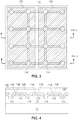
- FIG. 3 is a plan view and Figs. 4 and 5 are cross sectional views of such a device.
- an epitaxial structure 110 including a light emitting region disposed between an n-type region and a p-type region, is grown on a substrate 10.
- the n-contact metal layer 114 directly connected to the n-type region is distributed over a plurality of vias etched through the epitaxial structure to expose an n-type layer.
- the n-contact metal 114 in a given via is electrically connected to the n-contact metal in other vias by horizontal and vertical interconnects 118.
- the width of interconnects 118 may be, for example, on the order of 10 microns.
- the thickness of interconnects 118 may be, for example, on the order of several microns.
- Connection layers 122 and 124 make electrical connection between the light emitting device and a mount on which the light emitting device is mounted, while providing a thermal path for heat removal during operation.
- Connection layers 122 and 124 may be solder layers, or any other type of conductive connection between the sub mount and the device such as elemental metals, metal alloys, semiconductor-metal alloys, thermally and electrically conductive pastes or compounds (e.g. epoxies), eutectic joints between dissimilar metals between the light emitting device and the sub mount (e.g. Pd--In--Pd), gold stud-bumps, or solder bumps.
- Connection layer 122 connects to portions of the p-contact of the device, and connection layer 124 connects to some of the n-contact metals 114 deposited in the vias and the interconnects 118 electrically connecting the n-contact metals 114 in individual vias.
- the n-contact metals 114 and interconnects 118 may form a grid over the device. Though only the n-contacts 114 within the vias directly contact the n-type layer, interconnects 118 are electrically connected to the vias and are thus electrically connected to the n-type layers. In contrast to a device with a single large n-contact, n-contact metals 114 within the vias and interconnects 118 are not confined to a particular area on the chip. Similarly, the grid formed by n-contact metals 114 within the vias and interconnects 118 encloses an array of nine p-contact sections, at least some of which are available as p-contacts to a mount.
- connection layers 122 and 124 are not limited by the shape and location of the p- and n-contacts.
- Fig. 4 is a cross section of the device shown in Fig. 3 , taken along the axis shown in Fig. 3 .
- the n-contact metals 114 within the vias are isolated from the p-type layers and p-metal contacts 112 by dielectric layer 116.
- An n-metal layer may then be deposited over the entire chip and patterned to form n-contacts 114 in the vias and interconnects 118.
- a horizontal interconnect 118 is shown in Fig. 4 .
- a second dielectric layer 120 is then deposited over the chip.
- the second dielectric layer 120 is patterned to create a first set of openings aligned with p-metal regions 112 on the left side of the device underlying connection layer 122, and a second set of openings aligned with the n-contact metal 114 within the vias and interconnects 118 on the right side of the device underlying connection 124. Since connection layer 122 is the p-contact to the mount, dielectric layer 120 isolates connection layer 122 from interconnect 118. Since connection layer 124 is the n-contact to the mount, dielectric layer 120 is removed from the interconnects and vias underlying connection layer 124 such that connection layer 124 can make electrical contact with the n-contact metals 114 within the vias and interconnect 118.
- Fig. 5 is a cross section of the device shown in Fig. 3 , taken along the axis shown in Fig. 3 .
- Connection layer 122 makes contact to p-metal 112, thus in the area directly underlying connection layer 122, all of dielectric layer 120 is removed, except the portion covering interconnects 118.
- Connection layer 124 makes contact to the n-contacts and interconnects, thus in the area underlying connection layer 124 dielectric layer 120 is removed only from the top surface of interconnects 118.
- P-metal layer 112 is thus isolated from connection layer 124 by dielectric layer 120.
- Connection layers 122 and 124 need not be deposited as shown in Fig. 3 . Other configurations are possible by properly patterning dielectric layer 120.
- circuit elements such as capacitors, resistors, inductors, and diodes may be integrated into a semiconductor light emitting device between the semiconductor layers and the connection layers used to connect the device to a mount or other external device.
- Dielectric layers 116 and 120 shown in Figs. 4 and 5 which isolate the contact metals from the connection layers, facilitate the formation of the circuit elements.
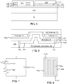
- Fig. 7 is a circuit diagram of an example of a device including integrated circuit elements, according to embodiments of the invention.
- a capacitor 164 and resistor 162 are formed between the semiconductor layers that form light emitting diode 110 and the connection layers used to connect the device to an external structure. Resistor 162 is connected in series and capacitor 164 is connected in parallel with light emitting diode 110.
- Fig. 6 is a cross sectional view of a portion of a device according to the circuit diagram shown in Fig. 7 .
- a mesa is formed in epitaxial structure 110, which includes one or more n-type layers, one or more light emitting layers, and one or more p-type layers.
- the mesa exposes an n-type layer on which n-contact 114 is formed.
- P-contacts 112 are formed on the remaining surface of epitaxial structure 110.
- P-contact 112 on the right side of the figure is connected to connection layer 122 through resistor 162, which is isolated from other metal layers in the device by dielectric layers 160a and 160b.
- a plan view of resistor 162 is shown in Fig. 8 .
- a thin metal layer 162a is formed between two dielectric segments 162b and 162c.
- the resistance of resistor 162 is controlled by adjusting the length of wire 162a.
- One end 162d of resistor 162 is connected to p-connection layer 122, and the other end 162e of resistor 162 is connected to p-contact 112.
- n-contact 114 is connected to n-connection layer 124 on the left side of the figure.
- a capacitor 164 is connected between p-connection layer 122 and n-contact 114.
- Dielectric layers 160b and 160c electrically isolate p-connection layer 122 from n-contact 114 and n-connection layer 124 in the vicinity of capacitor 164.
- a cross sectional view of capacitor 164 is shown in Fig. 9 .
- Stacks of metal layers form two plates of the capacitor, 164a and 164c.
- Each of the plates is shaped like a comb and arranged such that portions of plate 164a are interdigitated with portions of plate 164c.
- the two metal plates 164a and 164c are separated by a dielectric 164b.
- the top of plate 164a as shown in Fig. 9 is connected to n-contact 114 on the right side of capacitor 164 as shown in Fig. 6
- the bottom of plate 164c as shown in Fig. 9 is connected to p-connection layer 122 on the left side of capacitor 164 as shown in Fig. 6 .
- the capacitance of capacitor 164 is controlled by adjusting the overlapping area of and spacing between plates 164a and 164c.
- Fig. 11 is a circuit diagram of another example of a device including an integrated circuit element, according to embodiments of the invention.
- An electrostatic discharge (ESD) protection diode 172 is formed between the semiconductor layers that form light emitting diode 110 and between the connection layers used to connect the device to an external structure.
- Diode 172 is connected in anti-parallel configuration with light emitting diode 110.
- Diode 172 clamps reverse breakdown in light emitting diode 110.
- Fig. 10 is a cross sectional view of a portion of a device according to the circuit diagram shown in Fig. 11 .
- an n-contact 114 is connected to an n-type region in a mesa formed in epitaxial structure 110.
- P-contacts 112 are formed on the remaining surface of epitaxial structure 110.
- ESD protection diode 172 is disposed between p-connection layer 122 and n-contact 114.
- a p-type silicon layer 172a contacts n-contact 114
- an n-type silicon layer 172c contacts p-connection layer 122
- an i-type silicon layer 172b is disposed between p-type layer 172a and n-type layer 172c.
- ESD protection diode 172 may be a Schottky diode which includes an n-type or p-type silicon layer sandwiched between metal layers.
- the silicon layers of ESD protection diode 172 may be, for example, amorphous layers formed by plasma enhanced chemical vapor deposition (PECVD), or polycrystalline layers formed by laser pulsing or annealing after PECVD of amorphous layers. Silicon layers formed by PECVD may be deposited at temperatures low enough to avoid damage to other parts of the device such as epitaxial structure 110 and p- and n-contacts 112 and 114.
- silicon layers 172a, 172b, and 172c of ESD protection diode 172 may be formed at temperatures less than 250°C.
- silicon layers 172a is shown in direct contact with n-metal 114 and silicon layer 172c is shown in direct contact with connection 122.
- one or more additional metal layers may be disposed between silicon layers 172a and 172c and the metal layers to which they connect in Fig. 10 . These additional metal layers may be, for example, ohmic contacts to one or both of silicon layers 172a and 172c or guard metal layers.
- the p-n junction of ESD protection diode 172 shown in Fig. 10 is generally parallel to the p-n junction of light emitting diode 110.
- the perpendicular orientation of the p-n junction of diode element 50 in Fig. 2 relative to active region 33 limits the ability of diode element 50 to shunt current away from active region 33.
- the junction area of ESD protection diode 172 can be made much larger than that of diode element 50, which improves the ESD protection provided by diode 172.
- the light emitting region of Fig. 10 can be formed without removing part of the light emitting region to accommodate the ESD protection element.
- the light emitting region of Fig. 10 may be larger than active region 33 of Fig. 2 , potentially resulting in more light emission from the device of Fig. 10 .
- the device of Fig. 2 is likely not compatible with some growth substrate removal techniques such as laser melting, where the interface between the growth substrate and the epitaxial structure is exposed to laser light through the growth substrate, in order to melt the epitaxial material to remove the growth substrate. Exposure to the laser light required for growth substrate removal may damage the diode element.
- some growth substrate removal techniques such as laser melting
- ESD protection diode 172 is not “visible” through the growth substrate, since n-contact 114, which is typically opaque, is disposed between the growth substrate and ESD protection diode 172. Accordingly, ESD protection diode 172 is protected from the laser light required for laser melting by n-contact 114. Further, unlike diode element 50 which may reduce light extraction from the device by absorbing some light which otherwise might escape the semiconductor layers, ESD protection diode 172 does not block the path of light escaping from the semiconductor layers in the device.
- n-contact 114 is formed, it is to be understood that the devices of Figs. 6 and 10 may include multiple vias, as shown in Figs. 3-5 ; additional circuit elements may be formed near the via shown in Figs. 6 and 10 or near other vias that are not shown; and the circuit elements shown in Figs. 6 and 10 may extend across multiple vias.
- the circuit elements shown in the devices of Figs. 6 and 10 are merely examples of particular circuit elements and configurations, and are not meant to be limiting.
- the ESD protection diode shown in Fig. 10 may be combined with the metal and dielectric circuit elements shown in Fig. 6 .
- Embodiments of the invention include any circuit element that may be included in a device between the epitaxial layers and connection layers 122 and 124.
- the devices in Figs. 6 and 10 are shown in a flipped orientation, as when the device is mounted on a mount as a flip chip with the growth substrate (not shown) still attached or as a thin film device from which the growth substrate has been removed for example by laser melting, etching, or any other appropriate technique.
- p-contacts 112 and/or n-contacts 114 may be reflective, in order to direct light out the top of epitaxial structure 110.
- Fig. 10 shows a portion of mount 180, which may be any structure such as a reflector cup, printed circuit board, or package element such as a ceramic, semiconductor, or metal substrate.
- the epitaxial structure 110 is connected to mount 180 through connection layers 122 and 124.
- the device may be bonded to mount 180 on a wafer scale, such that an entire wafer of devices are bonded to a wafer of mounts, then the individual devices are diced after bonding.
- a wafer of devices may be diced into individual devices, and then each device bonded to mount 180 on a die scale, as described in more detail in U.S. Application Serial No. 10/977,294 , "Package-Integrated Thin-Film LED,” filed October 28, 2004, and incorporated herein by reference.
- Fig. 12 is an exploded view of a packaged light emitting device, as described in more detail in U.S. Patent 6,274,924 .
- a heat-sinking slug 100 is placed into an insert-molded lead frame.
- the insert-molded lead frame is, for example, a filled plastic material 105 molded around a metal frame 106 that provides an electrical path.
- Slug 100 may include an optional reflector cup 102.
- the light emitting device die 104 which may be any of the devices described in the embodiments above, is mounted directly or indirectly via a thermally conducting sub mount 103 to slug 100.
- a cover 108 which may be an optical lens, may be added.
- Fig. 13 is a cross sectional view of an alternative packaged light emitting device.
- the light emitting device die 104 which may be any of the devices described in the embodiments above, is mounted on a mount 187, which may be, for example, ceramic.
- Connection layers 122 and 124 connect die 104 to metal layers 185 and 186 on mount 187.
- Conductive vias 183 and 184 through the mount connect conductive mounting pads 181 and 182 to metal layers 185 and 186.
- One or more elements 192 such as, for example, a wavelength converting layer or layers, a mirror stack such as a Bragg reflector, an antireflective coating, and/or a dichroic filter may be disposed over die 104.
- a transparent material 194, which is shaped as a lens in Fig. 13 may cover the die.
- the structure shown in Fig. 13 may be connected to another structure, such as, for example, a PC board, metal core PC board, ceramic substrate, or direct bond copper substrate, by mounting pads 181
- III-nitride devices in other embodiments the devices may be formed form other materials systems, such as III-V devices including phosphorus or arsenic or II-VI devices. Therefore, it is not intended that the scope of the invention be limited to the specific embodiments illustrated and described. ayers stack.
Landscapes
- Led Device Packages (AREA)
- Led Devices (AREA)
- Semiconductor Integrated Circuits (AREA)
- Semiconductor Lasers (AREA)
Claims (11)
- Lichtemittierendes Halbleiterbauelement, umfassend:eine Halbleiterstruktur, die einen lichtemittierenden Bereich umfasst, der zwischen einem n-leitenden Bereich und einem p-leitenden Bereich angeordnet ist,eine erste Verbindungsschicht (124), die mit dem n-leitenden Bereich elektrisch verbunden ist, und eine zweite Verbindungsschicht (122), die mit dem p-leitenden Bereich elektrisch verbunden ist, wobei die erste und die zweite Verbindungsschicht dafür angeordnet sind, das lichtemittierende Halbleiterbauelement mit einem externen Bauelement zu verbinden,einen ersten Kontakt (114) in direktem Kontakt mit dem n-leitenden Bereich, wobei sich der erste Kontakt von der ersten Verbindungsschicht unterscheidet,einen zweiten Kontakt (112) in direktem Kontakt mit dem p-leitenden Bereich, wobei sich der zweite Kontakt von der zweiten Verbindungsschicht unterscheidet, undein Schaltkreiselement, das zwischen der Halbleiterstruktur und mindestens einem von der ersten Verbindungsschicht (124) und der zweiten Verbindungsschicht (122) angeordnet ist, wobei das Schaltkreiselement mindestens eine Metallschicht umfasst, die von einem Abschnitt des Bauelements durch eine dielektrische Schicht (120) isoliert ist, und wobei das Schaltkreiselement zwischen einem von dem ersten und dem zweiten Kontakt und einer von der ersten und der zweiten Verbindungsschicht elektrisch verbunden ist.
- Lichtemittierendes Halbleiterbauelement nach Anspruch 1, wobei das Schaltkreiselement einen Widerstand umfasst.
- Lichtemittierendes Halbleiterbauelement nach Anspruch 1, wobei das Schaltkreiselement einen Kondensator umfasst.
- Lichtemittierendes Halbleiterbauelement nach Anspruch 1, wobei das Schaltkreiselement einen Induktor umfasst.
- Lichtemittierendes Halbleiterbauelement nach Anspruch 1, wobei:
ein Abschnitt des ersten Kontakts (114) einen Abschnitt der zweiten Verbindungsschicht (122) überlagert und das Schaltkreiselement zwischen dem ersten Kontakt (114) und der zweiten Verbindungsschicht (122) angeordnet ist. - Lichtemittierendes Halbleiterbauelement nach Anspruch 1, ferner eine Abdeckung umfassend, die über dem lichtemittierenden Bereich angeordnet ist.
- Lichtemittierendes Halbleiterbauelement nach Anspruch 1, wobei das Schaltkreiselement ein zweites Schaltkreiselement ist und das Bauelement ferner ein erstes Schaltkreiselement (172) umfasst, das zwischen einem von dem ersten und dem zweiten Kontakt (114, 112) und einer von der ersten und der zweiten Verbindungsschicht (124, 122) elektrisch verbunden ist, wobei das erste Schaltkreiselement eine Diode umfasst, die mindestens eine Siliciumschicht umfasst, wobei die Diode einen p-i-n-Übergang oder einen Schottky-Übergang aufweist, der im Wesentlichen parallel zu dem p-n-Übergang des ersten lichtemittierenden Bereichs ist.
- Lichtemittierendes Halbleiterbauelement nach Anspruch 7, wobei der Diodenübergang einen Metall-Halbleiter-Übergang umfasst.
- Lichtemittierendes Halbleiterbauelement nach Anspruch 7, wobei das erste Schaltkreiselement (172) eine p-leitende Siliciumschicht umfasst, die mit dem ersten Kontakt und einer n-leitenden Siliciumschicht elektrisch verbunden ist, die mit der zweiten Verbindungsschicht elektrisch verbunden ist.
- Lichtemittierendes Halbleiterbauelement nach Anspruch 9, wobei das erste Schaltkreiselement (172) ferner eine i-leitende Siliciumschicht umfasst, die zwischen der p-leitenden Siliciumschicht und der n-leitenden Siliciumschicht angeordnet ist.
- Lichtemittierendes Halbleiterbauelement nach Anspruch 7, wobei der Diodenübergang in einer antiparallelen Konfiguration mit dem p-n-Übergang verbunden ist.
Applications Claiming Priority (2)
| Application Number | Priority Date | Filing Date | Title |
|---|---|---|---|
| US11/408,841 US7994514B2 (en) | 2006-04-21 | 2006-04-21 | Semiconductor light emitting device with integrated electronic components |
| PCT/IB2007/051372 WO2007122550A2 (en) | 2006-04-21 | 2007-04-17 | Semiconductor light emitting device with integrated electronic components |
Publications (2)
| Publication Number | Publication Date |
|---|---|
| EP2013908A2 EP2013908A2 (de) | 2009-01-14 |
| EP2013908B1 true EP2013908B1 (de) | 2019-06-12 |
Family
ID=38457716
Family Applications (1)
| Application Number | Title | Priority Date | Filing Date |
|---|---|---|---|
| EP07735517.0A Active EP2013908B1 (de) | 2006-04-21 | 2007-04-17 | Halbleiter-leuchtdiode mit integrierten elektronischen bauteilen |
Country Status (6)
| Country | Link |
|---|---|
| US (2) | US7994514B2 (de) |
| EP (1) | EP2013908B1 (de) |
| JP (3) | JP5462433B2 (de) |
| CN (1) | CN101427376B (de) |
| TW (1) | TWI425651B (de) |
| WO (1) | WO2007122550A2 (de) |
Families Citing this family (41)
| Publication number | Priority date | Publication date | Assignee | Title |
|---|---|---|---|---|
| DE102007022947B4 (de) | 2007-04-26 | 2022-05-05 | OSRAM Opto Semiconductors Gesellschaft mit beschränkter Haftung | Optoelektronischer Halbleiterkörper und Verfahren zur Herstellung eines solchen |
| US7738517B2 (en) * | 2007-10-29 | 2010-06-15 | Avago Technologies Fiber Ip (Singapore) Pte. Ltd. | Small form factor transmitter optical subassembly (TOSA) having functionality for controlling the temperature, and methods of making and using the TOSA |
| KR101438811B1 (ko) * | 2008-01-03 | 2014-09-05 | 엘지이노텍 주식회사 | 반도체 발광소자 및 그 제조방법 |
| US9113533B2 (en) | 2008-01-30 | 2015-08-18 | Koninklijke Philips N.V. | Semiconductor package with incorporated light or temperature sensors and time multiplexing |
| DE102008011848A1 (de) * | 2008-02-29 | 2009-09-03 | Osram Opto Semiconductors Gmbh | Optoelektronischer Halbleiterkörper und Verfahren zur Herstellung eines solchen |
| DE102008032318A1 (de) * | 2008-03-31 | 2009-10-01 | Osram Opto Semiconductors Gmbh | Optoelektronischer Halbleiterchip und Verfahren zur Herstellung eines solchen |
| DE102008034560B4 (de) * | 2008-07-24 | 2022-10-27 | OSRAM Opto Semiconductors Gesellschaft mit beschränkter Haftung | Strahlungsemittierender Halbleiterchip und Verfahren zur Herstellung eines strahlungsemittierenden Halbleiterchips |
| DE102009006177A1 (de) * | 2008-11-28 | 2010-06-02 | Osram Opto Semiconductors Gmbh | Strahlungsemittierender Halbleiterchip |
| KR20100076083A (ko) * | 2008-12-17 | 2010-07-06 | 서울반도체 주식회사 | 복수개의 발광셀들을 갖는 발광 다이오드 및 그것을 제조하는 방법 |
| JP5195452B2 (ja) * | 2009-01-22 | 2013-05-08 | ソニー株式会社 | 発光素子 |
| US7883910B2 (en) * | 2009-02-03 | 2011-02-08 | Industrial Technology Research Institute | Light emitting diode structure, LED packaging structure using the same and method of forming the same |
| JP2011119491A (ja) * | 2009-12-04 | 2011-06-16 | Showa Denko Kk | 半導体発光素子、電子機器および発光装置 |
| US9443834B2 (en) | 2010-09-02 | 2016-09-13 | Micron Technology, Inc. | Back-to-back solid state lighting devices and associated methods |
| KR101711961B1 (ko) | 2010-09-10 | 2017-03-03 | 삼성전자주식회사 | 발광 디바이스 |
| CN103222074B (zh) * | 2010-11-18 | 2016-06-01 | 首尔伟傲世有限公司 | 具有电极焊盘的发光二极管芯片 |
| US9520536B2 (en) | 2010-11-18 | 2016-12-13 | Seoul Viosys Co., Ltd. | Light emitting diode chip having electrode pad |
| JP5932851B2 (ja) * | 2011-03-14 | 2016-06-08 | コーニンクレッカ フィリップス エヌ ヴェKoninklijke Philips N.V. | Led構造体及びその形成方法 |
| US8315287B1 (en) | 2011-05-03 | 2012-11-20 | Avago Technologies Fiber Ip (Singapore) Pte. Ltd | Surface-emitting semiconductor laser device in which an edge-emitting laser is integrated with a diffractive lens, and a method for making the device |
| US20130001596A1 (en) * | 2011-06-28 | 2013-01-03 | Osram Sylvania Inc. | Deposition of esd protection on printed circuit boards |
| US8488645B2 (en) | 2011-07-31 | 2013-07-16 | Avago Technologies General Ip (Singapore) Pte. Ltd. | Semiconductor device having a vertical cavity surface emitting laser (VCSEL) and a protection diode integrated therein and having reduced capacitance to allow the VCSEL to achieve high operating speeds |
| US8809897B2 (en) * | 2011-08-31 | 2014-08-19 | Micron Technology, Inc. | Solid state transducer devices, including devices having integrated electrostatic discharge protection, and associated systems and methods |
| US9490239B2 (en) | 2011-08-31 | 2016-11-08 | Micron Technology, Inc. | Solid state transducers with state detection, and associated systems and methods |
| US20150001570A1 (en) * | 2011-09-02 | 2015-01-01 | King Dragon International Inc. | LED Package and Method of the Same |
| US9117941B2 (en) * | 2011-09-02 | 2015-08-25 | King Dragon International Inc. | LED package and method of the same |
| GB2502311A (en) | 2012-05-24 | 2013-11-27 | Ibm | Photovoltaic device with band-stop filter |
| CN103474522B (zh) * | 2012-06-07 | 2016-04-13 | 清华大学 | 发光二极管的制备方法 |
| JP5989420B2 (ja) * | 2012-06-28 | 2016-09-07 | 株式会社東芝 | 半導体発光装置 |
| DE102013103079A1 (de) * | 2013-03-26 | 2014-10-02 | Osram Opto Semiconductors Gmbh | Optoelektronischer Halbleiterchip und Verfahren zur Herstellung eines optoelektronischen Halbleiterchips |
| KR102085897B1 (ko) * | 2013-06-10 | 2020-03-06 | 엘지이노텍 주식회사 | 발광 소자 및 발광 소자 패키지 |
| DE102013107531A1 (de) * | 2013-07-16 | 2015-01-22 | Osram Opto Semiconductors Gmbh | Optoelektronischer Halbleiterchip |
| KR102222861B1 (ko) * | 2013-07-18 | 2021-03-04 | 루미리즈 홀딩 비.브이. | 고반사성 플립칩 led 다이 |
| JP6028690B2 (ja) * | 2013-08-06 | 2016-11-16 | 豊田合成株式会社 | Iii 族窒化物半導体発光素子 |
| DE102013112881A1 (de) * | 2013-11-21 | 2015-05-21 | Osram Opto Semiconductors Gmbh | Optoelektronischer Halbleiterchip |
| JP6468057B2 (ja) * | 2015-04-28 | 2019-02-13 | 日亜化学工業株式会社 | 発光素子 |
| DE102015114587A1 (de) * | 2015-09-01 | 2017-03-02 | Osram Opto Semiconductors Gmbh | Optoelektronisches Halbleiterbauelement und Verfahren zu dessen Herstellung |
| TWI563490B (en) | 2015-12-04 | 2016-12-21 | Ind Tech Res Inst | Display pixel and display panel |
| KR101845611B1 (ko) * | 2016-07-13 | 2018-04-04 | 고려대학교 산학협력단 | 발광창 전극 구조가 구비된 고효율 발광다이오드 제작 방법 |
| CN107134448B (zh) * | 2017-04-18 | 2019-04-02 | 中国科学院半导体研究所 | 提高可见光通信led光源调制带宽的可集成化方法 |
| DE102017122111B4 (de) * | 2017-09-25 | 2024-03-07 | OSRAM Opto Semiconductors Gesellschaft mit beschränkter Haftung | Elektronisches Bauteil |
| CN110731011B (zh) * | 2019-01-25 | 2023-08-22 | 厦门市三安光电科技有限公司 | 一种发光二极管器件 |
| CN116960150A (zh) | 2022-04-19 | 2023-10-27 | 联华电子股份有限公司 | 高电子迁移率晶体管 |
Family Cites Families (48)
| Publication number | Priority date | Publication date | Assignee | Title |
|---|---|---|---|---|
| US2017A (en) * | 1841-03-26 | The graphic co | ||
| US3012A (en) * | 1843-03-21 | Machine fob | ||
| US3018A (en) * | 1843-03-21 | Coupling for qttilting-frames | ||
| US5020A (en) * | 1847-03-20 | Brussels loom | ||
| FR2319267A1 (fr) | 1973-07-03 | 1977-02-18 | Radiotechnique Compelec | Dispositif electroluminescent a seuil |
| JPS6245193A (ja) * | 1985-08-23 | 1987-02-27 | Hitachi Ltd | 光電子装置 |
| EP0326615B1 (de) * | 1986-09-19 | 1993-11-10 | Kabushiki Kaisha Komatsu Seisakusho | Dünnfilmanordnung |
| JPH02292881A (ja) * | 1989-05-01 | 1990-12-04 | Sumitomo Electric Ind Ltd | 半導体レーザの保護回路 |
| US5483085A (en) * | 1994-05-09 | 1996-01-09 | Motorola, Inc. | Electro-optic integrated circuit with diode decoder |
| JP3447527B2 (ja) * | 1996-09-09 | 2003-09-16 | 株式会社東芝 | 半導体発光素子およびその製造方法 |
| TW365071B (en) * | 1996-09-09 | 1999-07-21 | Toshiba Corp | Semiconductor light emitting diode and method for manufacturing the same |
| US6054716A (en) * | 1997-01-10 | 2000-04-25 | Rohm Co., Ltd. | Semiconductor light emitting device having a protecting device |
| EP1959506A2 (de) * | 1997-01-31 | 2008-08-20 | Matsushita Electric Industrial Co., Ltd. | Herstellungsverfahren für eine lichtemittierende Halbleitervorrichtung |
| JP3572924B2 (ja) * | 1997-03-06 | 2004-10-06 | 松下電器産業株式会社 | 発光装置及びそれを用いた記録装置 |
| JPH10270753A (ja) * | 1997-03-21 | 1998-10-09 | Sanyo Electric Co Ltd | 半導体発光素子および表示装置 |
| WO1998052229A1 (en) * | 1997-05-14 | 1998-11-19 | Research Triangle Institute | Light emitting device contact layers having substantially equal spreading resistance and method of manufacture |
| JP3257455B2 (ja) * | 1997-07-17 | 2002-02-18 | 松下電器産業株式会社 | 発光装置 |
| EP1014455B1 (de) * | 1997-07-25 | 2006-07-12 | Nichia Corporation | Halbleitervorrichtung aus einer nitridverbindung |
| JPH11307315A (ja) * | 1998-04-22 | 1999-11-05 | Advantest Corp | 可変抵抗及びパルス幅可変電気パルス発生回路 |
| JP2000022128A (ja) * | 1998-07-06 | 2000-01-21 | Murata Mfg Co Ltd | 半導体発光素子、および光電子集積回路素子 |
| JP2000077765A (ja) * | 1998-09-01 | 2000-03-14 | Matsushita Electric Ind Co Ltd | レーザダイオード発光デバイス |
| US6274924B1 (en) * | 1998-11-05 | 2001-08-14 | Lumileds Lighting, U.S. Llc | Surface mountable LED package |
| US6838705B1 (en) * | 1999-03-29 | 2005-01-04 | Nichia Corporation | Nitride semiconductor device |
| US6229181B1 (en) * | 1999-04-30 | 2001-05-08 | Digital Devices, Inc. | Semiconductor device and method of forming a semiconductor structure to provide electrostatic discharge protection |
| US6486499B1 (en) * | 1999-12-22 | 2002-11-26 | Lumileds Lighting U.S., Llc | III-nitride light-emitting device with increased light generating capability |
| US6433985B1 (en) * | 1999-12-30 | 2002-08-13 | International Business Machines Corporation | ESD network with capacitor blocking element |
| US6480110B2 (en) * | 2000-12-01 | 2002-11-12 | Microchip Technology Incorporated | Inductively tunable antenna for a radio frequency identification tag |
| US6547249B2 (en) * | 2001-03-29 | 2003-04-15 | Lumileds Lighting U.S., Llc | Monolithic series/parallel led arrays formed on highly resistive substrates |
| JP2002314136A (ja) * | 2001-04-09 | 2002-10-25 | Toyoda Gosei Co Ltd | 半導体発光装置 |
| TW492202B (en) * | 2001-06-05 | 2002-06-21 | South Epitaxy Corp | Structure of III-V light emitting diode (LED) arranged in flip chip configuration having structure for preventing electrostatic discharge |
| JP2003197754A (ja) * | 2001-12-26 | 2003-07-11 | Mitsubishi Electric Corp | 高周波半導体装置 |
| TW545698U (en) * | 2001-12-28 | 2003-08-01 | United Epitaxy Co Ltd | LED packaging structure with a static charge protecting device |
| TW535307B (en) * | 2002-03-04 | 2003-06-01 | United Epitaxy Co Ltd | Package of light emitting diode with protective diode |
| JP2003332626A (ja) * | 2002-05-08 | 2003-11-21 | Matsushita Electric Ind Co Ltd | 半導体発光装置 |
| JP2004006548A (ja) * | 2002-06-03 | 2004-01-08 | Renesas Technology Corp | 半導体レーザ素子及びその製造方法 |
| US6828596B2 (en) * | 2002-06-13 | 2004-12-07 | Lumileds Lighting U.S., Llc | Contacting scheme for large and small area semiconductor light emitting flip chip devices |
| US6642550B1 (en) * | 2002-08-26 | 2003-11-04 | California Micro Devices | Silicon sub-mount capable of single wire bonding and of providing ESD protection for light emitting diode devices |
| JP4299580B2 (ja) * | 2003-05-16 | 2009-07-22 | 住友化学株式会社 | 発光素子および発光装置 |
| JP2004048067A (ja) * | 2003-10-14 | 2004-02-12 | Sanyo Electric Co Ltd | 発光部品およびその製造方法 |
| TWI223889B (en) * | 2004-01-20 | 2004-11-11 | Opto Tech Corp | Light-emitting device capable of preventing electrostatic damage |
| JP4577497B2 (ja) * | 2004-02-02 | 2010-11-10 | サンケン電気株式会社 | 半導体発光素子と保護素子との複合半導体装置 |
| TWI260795B (en) * | 2004-03-22 | 2006-08-21 | South Epitaxy Corp | Flip chip type- light emitting diode package |
| US7064353B2 (en) * | 2004-05-26 | 2006-06-20 | Philips Lumileds Lighting Company, Llc | LED chip with integrated fast switching diode for ESD protection |
| JP2006066846A (ja) * | 2004-07-29 | 2006-03-09 | Seiko Epson Corp | 面発光型装置及びその製造方法 |
| JP2006086300A (ja) * | 2004-09-15 | 2006-03-30 | Sanken Electric Co Ltd | 保護素子を有する半導体発光装置及びその製造方法 |
| KR100576872B1 (ko) * | 2004-09-17 | 2006-05-10 | 삼성전기주식회사 | 정전기 방전 방지기능을 갖는 질화물 반도체 발광소자 |
| TWI244748B (en) | 2004-10-08 | 2005-12-01 | Epistar Corp | A light-emitting device with a protecting structure |
| US7535028B2 (en) * | 2005-02-03 | 2009-05-19 | Ac Led Lighting, L.Lc. | Micro-LED based high voltage AC/DC indicator lamp |
-
2006
- 2006-04-21 US US11/408,841 patent/US7994514B2/en active Active
-
2007
- 2007-04-17 CN CN2007800142710A patent/CN101427376B/zh active Active
- 2007-04-17 EP EP07735517.0A patent/EP2013908B1/de active Active
- 2007-04-17 WO PCT/IB2007/051372 patent/WO2007122550A2/en not_active Ceased
- 2007-04-18 TW TW096113664A patent/TWI425651B/zh active
- 2007-04-20 JP JP2007136000A patent/JP5462433B2/ja active Active
-
2011
- 2011-04-01 US US13/078,036 patent/US8450760B2/en not_active Expired - Lifetime
-
2012
- 2012-12-18 JP JP2012276149A patent/JP5813620B2/ja active Active
-
2013
- 2013-10-07 JP JP2013210290A patent/JP5744147B2/ja active Active
Also Published As
| Publication number | Publication date |
|---|---|
| EP2013908A2 (de) | 2009-01-14 |
| JP2014030051A (ja) | 2014-02-13 |
| JP2013102168A (ja) | 2013-05-23 |
| US20110175138A1 (en) | 2011-07-21 |
| CN101427376B (zh) | 2010-12-08 |
| US7994514B2 (en) | 2011-08-09 |
| JP5462433B2 (ja) | 2014-04-02 |
| US20070246716A1 (en) | 2007-10-25 |
| WO2007122550A2 (en) | 2007-11-01 |
| JP5744147B2 (ja) | 2015-07-01 |
| TWI425651B (zh) | 2014-02-01 |
| JP2007294981A (ja) | 2007-11-08 |
| CN101427376A (zh) | 2009-05-06 |
| TW200746477A (en) | 2007-12-16 |
| US8450760B2 (en) | 2013-05-28 |
| WO2007122550A3 (en) | 2008-03-06 |
| JP5813620B2 (ja) | 2015-11-17 |
Similar Documents
| Publication | Publication Date | Title |
|---|---|---|
| EP2013908B1 (de) | Halbleiter-leuchtdiode mit integrierten elektronischen bauteilen | |
| US10950755B2 (en) | Light emitting diode, method of fabricating the same and LED module having the same | |
| US10062810B2 (en) | Light-emitting diode module having light-emitting diode joined through solder paste and light-emitting diode | |
| US9640719B2 (en) | Light emitting diode, method of fabricating the same and LED module having the same | |
| US6876008B2 (en) | Mount for semiconductor light emitting device | |
| KR102135624B1 (ko) | 발광 다이오드 및 그것을 갖는 발광 다이오드 모듈 | |
| US20100201280A1 (en) | Electrically isolated vertical light emitting diode structure | |
| KR20150014353A (ko) | 발광 다이오드 | |
| KR102091842B1 (ko) | 발광 다이오드 및 그것을 제조하는 방법 | |
| JP2006073618A (ja) | 光学素子およびその製造方法 | |
| KR20160056066A (ko) | 발광소자 | |
| KR102002618B1 (ko) | 발광 다이오드 | |
| KR102149911B1 (ko) | 발광 다이오드 및 그것을 갖는 발광 다이오드 모듈 | |
| KR101502835B1 (ko) | Led용 서브마운트, led칩 및 led칩 제조방법 | |
| KR102002617B1 (ko) | 발광 다이오드 | |
| KR20180122884A (ko) | 반도체소자 |
Legal Events
| Date | Code | Title | Description |
|---|---|---|---|
| PUAI | Public reference made under article 153(3) epc to a published international application that has entered the european phase |
Free format text: ORIGINAL CODE: 0009012 |
|
| 17P | Request for examination filed |
Effective date: 20081121 |
|
| AK | Designated contracting states |
Kind code of ref document: A2 Designated state(s): AT BE BG CH CY CZ DE DK EE ES FI FR GB GR HU IE IS IT LI LT LU LV MC MT NL PL PT RO SE SI SK TR |
|
| AX | Request for extension of the european patent |
Extension state: AL BA HR MK RS |
|
| DAX | Request for extension of the european patent (deleted) | ||
| RAP1 | Party data changed (applicant data changed or rights of an application transferred) |
Owner name: KONINKLIJKE PHILIPS N.V. Owner name: PHILIPS LUMILEDS LIGHTING COMPANY LLC |
|
| 17Q | First examination report despatched |
Effective date: 20140728 |
|
| STAA | Information on the status of an ep patent application or granted ep patent |
Free format text: STATUS: EXAMINATION IS IN PROGRESS |
|
| RAP1 | Party data changed (applicant data changed or rights of an application transferred) |
Owner name: KONINKLIJKE PHILIPS N.V. Owner name: LUMILEDS LLC |
|
| RAP1 | Party data changed (applicant data changed or rights of an application transferred) |
Owner name: LUMILEDS HOLDING B.V. |
|
| GRAP | Despatch of communication of intention to grant a patent |
Free format text: ORIGINAL CODE: EPIDOSNIGR1 |
|
| STAA | Information on the status of an ep patent application or granted ep patent |
Free format text: STATUS: GRANT OF PATENT IS INTENDED |
|
| INTG | Intention to grant announced |
Effective date: 20190104 |
|
| GRAS | Grant fee paid |
Free format text: ORIGINAL CODE: EPIDOSNIGR3 |
|
| GRAA | (expected) grant |
Free format text: ORIGINAL CODE: 0009210 |
|
| STAA | Information on the status of an ep patent application or granted ep patent |
Free format text: STATUS: THE PATENT HAS BEEN GRANTED |
|
| AK | Designated contracting states |
Kind code of ref document: B1 Designated state(s): AT BE BG CH CY CZ DE DK EE ES FI FR GB GR HU IE IS IT LI LT LU LV MC MT NL PL PT RO SE SI SK TR |
|
| REG | Reference to a national code |
Ref country code: GB Ref legal event code: FG4D |
|
| REG | Reference to a national code |
Ref country code: CH Ref legal event code: EP |
|
| REG | Reference to a national code |
Ref country code: AT Ref legal event code: REF Ref document number: 1143708 Country of ref document: AT Kind code of ref document: T Effective date: 20190615 |
|
| REG | Reference to a national code |
Ref country code: DE Ref legal event code: R096 Ref document number: 602007058573 Country of ref document: DE |
|
| REG | Reference to a national code |
Ref country code: IE Ref legal event code: FG4D |
|
| REG | Reference to a national code |
Ref country code: NL Ref legal event code: MP Effective date: 20190612 |
|
| REG | Reference to a national code |
Ref country code: LT Ref legal event code: MG4D |
|
| PG25 | Lapsed in a contracting state [announced via postgrant information from national office to epo] |
Ref country code: LT Free format text: LAPSE BECAUSE OF FAILURE TO SUBMIT A TRANSLATION OF THE DESCRIPTION OR TO PAY THE FEE WITHIN THE PRESCRIBED TIME-LIMIT Effective date: 20190612 Ref country code: ES Free format text: LAPSE BECAUSE OF FAILURE TO SUBMIT A TRANSLATION OF THE DESCRIPTION OR TO PAY THE FEE WITHIN THE PRESCRIBED TIME-LIMIT Effective date: 20190612 Ref country code: FI Free format text: LAPSE BECAUSE OF FAILURE TO SUBMIT A TRANSLATION OF THE DESCRIPTION OR TO PAY THE FEE WITHIN THE PRESCRIBED TIME-LIMIT Effective date: 20190612 Ref country code: SE Free format text: LAPSE BECAUSE OF FAILURE TO SUBMIT A TRANSLATION OF THE DESCRIPTION OR TO PAY THE FEE WITHIN THE PRESCRIBED TIME-LIMIT Effective date: 20190612 |
|
| PG25 | Lapsed in a contracting state [announced via postgrant information from national office to epo] |
Ref country code: BG Free format text: LAPSE BECAUSE OF FAILURE TO SUBMIT A TRANSLATION OF THE DESCRIPTION OR TO PAY THE FEE WITHIN THE PRESCRIBED TIME-LIMIT Effective date: 20190912 Ref country code: GR Free format text: LAPSE BECAUSE OF FAILURE TO SUBMIT A TRANSLATION OF THE DESCRIPTION OR TO PAY THE FEE WITHIN THE PRESCRIBED TIME-LIMIT Effective date: 20190913 Ref country code: LV Free format text: LAPSE BECAUSE OF FAILURE TO SUBMIT A TRANSLATION OF THE DESCRIPTION OR TO PAY THE FEE WITHIN THE PRESCRIBED TIME-LIMIT Effective date: 20190612 |
|
| REG | Reference to a national code |
Ref country code: AT Ref legal event code: MK05 Ref document number: 1143708 Country of ref document: AT Kind code of ref document: T Effective date: 20190612 |
|
| PG25 | Lapsed in a contracting state [announced via postgrant information from national office to epo] |
Ref country code: EE Free format text: LAPSE BECAUSE OF FAILURE TO SUBMIT A TRANSLATION OF THE DESCRIPTION OR TO PAY THE FEE WITHIN THE PRESCRIBED TIME-LIMIT Effective date: 20190612 Ref country code: NL Free format text: LAPSE BECAUSE OF FAILURE TO SUBMIT A TRANSLATION OF THE DESCRIPTION OR TO PAY THE FEE WITHIN THE PRESCRIBED TIME-LIMIT Effective date: 20190612 Ref country code: AT Free format text: LAPSE BECAUSE OF FAILURE TO SUBMIT A TRANSLATION OF THE DESCRIPTION OR TO PAY THE FEE WITHIN THE PRESCRIBED TIME-LIMIT Effective date: 20190612 Ref country code: RO Free format text: LAPSE BECAUSE OF FAILURE TO SUBMIT A TRANSLATION OF THE DESCRIPTION OR TO PAY THE FEE WITHIN THE PRESCRIBED TIME-LIMIT Effective date: 20190612 Ref country code: CZ Free format text: LAPSE BECAUSE OF FAILURE TO SUBMIT A TRANSLATION OF THE DESCRIPTION OR TO PAY THE FEE WITHIN THE PRESCRIBED TIME-LIMIT Effective date: 20190612 Ref country code: PT Free format text: LAPSE BECAUSE OF FAILURE TO SUBMIT A TRANSLATION OF THE DESCRIPTION OR TO PAY THE FEE WITHIN THE PRESCRIBED TIME-LIMIT Effective date: 20191014 Ref country code: SK Free format text: LAPSE BECAUSE OF FAILURE TO SUBMIT A TRANSLATION OF THE DESCRIPTION OR TO PAY THE FEE WITHIN THE PRESCRIBED TIME-LIMIT Effective date: 20190612 |
|
| PG25 | Lapsed in a contracting state [announced via postgrant information from national office to epo] |
Ref country code: IS Free format text: LAPSE BECAUSE OF FAILURE TO SUBMIT A TRANSLATION OF THE DESCRIPTION OR TO PAY THE FEE WITHIN THE PRESCRIBED TIME-LIMIT Effective date: 20191012 Ref country code: IT Free format text: LAPSE BECAUSE OF FAILURE TO SUBMIT A TRANSLATION OF THE DESCRIPTION OR TO PAY THE FEE WITHIN THE PRESCRIBED TIME-LIMIT Effective date: 20190612 |
|
| REG | Reference to a national code |
Ref country code: DE Ref legal event code: R097 Ref document number: 602007058573 Country of ref document: DE |
|
| PG25 | Lapsed in a contracting state [announced via postgrant information from national office to epo] |
Ref country code: TR Free format text: LAPSE BECAUSE OF FAILURE TO SUBMIT A TRANSLATION OF THE DESCRIPTION OR TO PAY THE FEE WITHIN THE PRESCRIBED TIME-LIMIT Effective date: 20190612 |
|
| PLBE | No opposition filed within time limit |
Free format text: ORIGINAL CODE: 0009261 |
|
| STAA | Information on the status of an ep patent application or granted ep patent |
Free format text: STATUS: NO OPPOSITION FILED WITHIN TIME LIMIT |
|
| PG25 | Lapsed in a contracting state [announced via postgrant information from national office to epo] |
Ref country code: DK Free format text: LAPSE BECAUSE OF FAILURE TO SUBMIT A TRANSLATION OF THE DESCRIPTION OR TO PAY THE FEE WITHIN THE PRESCRIBED TIME-LIMIT Effective date: 20190612 Ref country code: PL Free format text: LAPSE BECAUSE OF FAILURE TO SUBMIT A TRANSLATION OF THE DESCRIPTION OR TO PAY THE FEE WITHIN THE PRESCRIBED TIME-LIMIT Effective date: 20190612 |
|
| 26N | No opposition filed |
Effective date: 20200313 |
|
| PG25 | Lapsed in a contracting state [announced via postgrant information from national office to epo] |
Ref country code: IS Free format text: LAPSE BECAUSE OF FAILURE TO SUBMIT A TRANSLATION OF THE DESCRIPTION OR TO PAY THE FEE WITHIN THE PRESCRIBED TIME-LIMIT Effective date: 20200224 Ref country code: SI Free format text: LAPSE BECAUSE OF FAILURE TO SUBMIT A TRANSLATION OF THE DESCRIPTION OR TO PAY THE FEE WITHIN THE PRESCRIBED TIME-LIMIT Effective date: 20190612 |
|
| PG2D | Information on lapse in contracting state deleted |
Ref country code: IS |
|
| PG25 | Lapsed in a contracting state [announced via postgrant information from national office to epo] |
Ref country code: IS Free format text: LAPSE BECAUSE OF FAILURE TO SUBMIT A TRANSLATION OF THE DESCRIPTION OR TO PAY THE FEE WITHIN THE PRESCRIBED TIME-LIMIT Effective date: 20191112 |
|
| PG25 | Lapsed in a contracting state [announced via postgrant information from national office to epo] |
Ref country code: MC Free format text: LAPSE BECAUSE OF FAILURE TO SUBMIT A TRANSLATION OF THE DESCRIPTION OR TO PAY THE FEE WITHIN THE PRESCRIBED TIME-LIMIT Effective date: 20190612 |
|
| REG | Reference to a national code |
Ref country code: CH Ref legal event code: PL |
|
| PG25 | Lapsed in a contracting state [announced via postgrant information from national office to epo] |
Ref country code: LI Free format text: LAPSE BECAUSE OF NON-PAYMENT OF DUE FEES Effective date: 20200430 Ref country code: LU Free format text: LAPSE BECAUSE OF NON-PAYMENT OF DUE FEES Effective date: 20200417 Ref country code: CH Free format text: LAPSE BECAUSE OF NON-PAYMENT OF DUE FEES Effective date: 20200430 |
|
| REG | Reference to a national code |
Ref country code: BE Ref legal event code: MM Effective date: 20200430 |
|
| PG25 | Lapsed in a contracting state [announced via postgrant information from national office to epo] |
Ref country code: BE Free format text: LAPSE BECAUSE OF NON-PAYMENT OF DUE FEES Effective date: 20200430 |
|
| PG25 | Lapsed in a contracting state [announced via postgrant information from national office to epo] |
Ref country code: IE Free format text: LAPSE BECAUSE OF NON-PAYMENT OF DUE FEES Effective date: 20200417 |
|
| PG25 | Lapsed in a contracting state [announced via postgrant information from national office to epo] |
Ref country code: MT Free format text: LAPSE BECAUSE OF FAILURE TO SUBMIT A TRANSLATION OF THE DESCRIPTION OR TO PAY THE FEE WITHIN THE PRESCRIBED TIME-LIMIT Effective date: 20190612 Ref country code: CY Free format text: LAPSE BECAUSE OF FAILURE TO SUBMIT A TRANSLATION OF THE DESCRIPTION OR TO PAY THE FEE WITHIN THE PRESCRIBED TIME-LIMIT Effective date: 20190612 |
|
| P01 | Opt-out of the competence of the unified patent court (upc) registered |
Effective date: 20230530 |
|
| REG | Reference to a national code |
Ref country code: DE Ref legal event code: R079 Ref document number: 602007058573 Country of ref document: DE Free format text: PREVIOUS MAIN CLASS: H01L0027150000 Ipc: H10H0029140000 |
|
| PGFP | Annual fee paid to national office [announced via postgrant information from national office to epo] |
Ref country code: DE Payment date: 20250428 Year of fee payment: 19 |
|
| PGFP | Annual fee paid to national office [announced via postgrant information from national office to epo] |
Ref country code: FR Payment date: 20250424 Year of fee payment: 19 |
|
| PGFP | Annual fee paid to national office [announced via postgrant information from national office to epo] |
Ref country code: GB Payment date: 20260225 Year of fee payment: 20 |