EP2012371B1 - Method for fabricating a semiconductor light emitting device - Google Patents
Method for fabricating a semiconductor light emitting device Download PDFInfo
- Publication number
- EP2012371B1 EP2012371B1 EP07741629.5A EP07741629A EP2012371B1 EP 2012371 B1 EP2012371 B1 EP 2012371B1 EP 07741629 A EP07741629 A EP 07741629A EP 2012371 B1 EP2012371 B1 EP 2012371B1
- Authority
- EP
- European Patent Office
- Prior art keywords
- izo film
- emitting device
- semiconductor light
- layer
- light
- Prior art date
- Legal status (The legal status is an assumption and is not a legal conclusion. Google has not performed a legal analysis and makes no representation as to the accuracy of the status listed.)
- Active
Links
- 239000004065 semiconductor Substances 0.000 title claims description 123
- 238000000034 method Methods 0.000 title claims description 84
- 239000010410 layer Substances 0.000 claims description 96
- 238000000137 annealing Methods 0.000 claims description 63
- 230000008569 process Effects 0.000 claims description 51
- 238000004519 manufacturing process Methods 0.000 claims description 25
- 239000012298 atmosphere Substances 0.000 claims description 21
- 239000011241 protective layer Substances 0.000 claims description 8
- 238000000059 patterning Methods 0.000 claims description 4
- 230000008859 change Effects 0.000 claims description 3
- 239000010408 film Substances 0.000 description 144
- 229910002601 GaN Inorganic materials 0.000 description 62
- 238000002834 transmittance Methods 0.000 description 28
- -1 gallium nitride compound Chemical class 0.000 description 26
- 239000000758 substrate Substances 0.000 description 19
- 239000013078 crystal Substances 0.000 description 15
- 230000000052 comparative effect Effects 0.000 description 14
- 239000007789 gas Substances 0.000 description 13
- 239000012299 nitrogen atmosphere Substances 0.000 description 10
- 239000010931 gold Substances 0.000 description 7
- 239000000463 material Substances 0.000 description 7
- 229910052751 metal Inorganic materials 0.000 description 7
- 239000002184 metal Substances 0.000 description 7
- 238000002441 X-ray diffraction Methods 0.000 description 6
- PJXISJQVUVHSOJ-UHFFFAOYSA-N indium(III) oxide Inorganic materials [O-2].[O-2].[O-2].[In+3].[In+3] PJXISJQVUVHSOJ-UHFFFAOYSA-N 0.000 description 5
- 239000000203 mixture Substances 0.000 description 5
- 229910052594 sapphire Inorganic materials 0.000 description 5
- 239000010980 sapphire Substances 0.000 description 5
- 238000004544 sputter deposition Methods 0.000 description 5
- 239000011521 glass Substances 0.000 description 4
- 239000011777 magnesium Substances 0.000 description 4
- IJGRMHOSHXDMSA-UHFFFAOYSA-N Atomic nitrogen Chemical compound N#N IJGRMHOSHXDMSA-UHFFFAOYSA-N 0.000 description 3
- OAKJQQAXSVQMHS-UHFFFAOYSA-N Hydrazine Chemical compound NN OAKJQQAXSVQMHS-UHFFFAOYSA-N 0.000 description 3
- QVGXLLKOCUKJST-UHFFFAOYSA-N atomic oxygen Chemical compound [O] QVGXLLKOCUKJST-UHFFFAOYSA-N 0.000 description 3
- 238000005530 etching Methods 0.000 description 3
- 229910052737 gold Inorganic materials 0.000 description 3
- 238000001451 molecular beam epitaxy Methods 0.000 description 3
- 239000001301 oxygen Substances 0.000 description 3
- 229910052760 oxygen Inorganic materials 0.000 description 3
- 239000002245 particle Substances 0.000 description 3
- 229910002704 AlGaN Inorganic materials 0.000 description 2
- BLRPTPMANUNPDV-UHFFFAOYSA-N Silane Chemical compound [SiH4] BLRPTPMANUNPDV-UHFFFAOYSA-N 0.000 description 2
- VYPSYNLAJGMNEJ-UHFFFAOYSA-N Silicium dioxide Chemical compound O=[Si]=O VYPSYNLAJGMNEJ-UHFFFAOYSA-N 0.000 description 2
- PNEYBMLMFCGWSK-UHFFFAOYSA-N aluminium oxide Inorganic materials [O-2].[O-2].[O-2].[Al+3].[Al+3] PNEYBMLMFCGWSK-UHFFFAOYSA-N 0.000 description 2
- 238000005229 chemical vapour deposition Methods 0.000 description 2
- 229910052593 corundum Inorganic materials 0.000 description 2
- 238000002425 crystallisation Methods 0.000 description 2
- 230000008025 crystallization Effects 0.000 description 2
- 239000002019 doping agent Substances 0.000 description 2
- 238000001312 dry etching Methods 0.000 description 2
- PCHJSUWPFVWCPO-UHFFFAOYSA-N gold Chemical compound [Au] PCHJSUWPFVWCPO-UHFFFAOYSA-N 0.000 description 2
- 238000002248 hydride vapour-phase epitaxy Methods 0.000 description 2
- AMGQUBHHOARCQH-UHFFFAOYSA-N indium;oxotin Chemical compound [In].[Sn]=O AMGQUBHHOARCQH-UHFFFAOYSA-N 0.000 description 2
- 238000001755 magnetron sputter deposition Methods 0.000 description 2
- 238000000206 photolithography Methods 0.000 description 2
- 239000011347 resin Substances 0.000 description 2
- 229920005989 resin Polymers 0.000 description 2
- 229910052596 spinel Inorganic materials 0.000 description 2
- XOLBLPGZBRYERU-UHFFFAOYSA-N tin dioxide Chemical compound O=[Sn]=O XOLBLPGZBRYERU-UHFFFAOYSA-N 0.000 description 2
- VOITXYVAKOUIBA-UHFFFAOYSA-N triethylaluminium Chemical compound CC[Al](CC)CC VOITXYVAKOUIBA-UHFFFAOYSA-N 0.000 description 2
- RGGPNXQUMRMPRA-UHFFFAOYSA-N triethylgallium Chemical compound CC[Ga](CC)CC RGGPNXQUMRMPRA-UHFFFAOYSA-N 0.000 description 2
- OTRPZROOJRIMKW-UHFFFAOYSA-N triethylindigane Chemical compound CC[In](CC)CC OTRPZROOJRIMKW-UHFFFAOYSA-N 0.000 description 2
- JLTRXTDYQLMHGR-UHFFFAOYSA-N trimethylaluminium Chemical compound C[Al](C)C JLTRXTDYQLMHGR-UHFFFAOYSA-N 0.000 description 2
- XCZXGTMEAKBVPV-UHFFFAOYSA-N trimethylgallium Chemical compound C[Ga](C)C XCZXGTMEAKBVPV-UHFFFAOYSA-N 0.000 description 2
- IBEFSUTVZWZJEL-UHFFFAOYSA-N trimethylindium Chemical compound C[In](C)C IBEFSUTVZWZJEL-UHFFFAOYSA-N 0.000 description 2
- 238000007740 vapor deposition Methods 0.000 description 2
- 238000001039 wet etching Methods 0.000 description 2
- 229910001845 yogo sapphire Inorganic materials 0.000 description 2
- QGZKDVFQNNGYKY-UHFFFAOYSA-N Ammonia Chemical compound N QGZKDVFQNNGYKY-UHFFFAOYSA-N 0.000 description 1
- QGZKDVFQNNGYKY-UHFFFAOYSA-O Ammonium Chemical compound [NH4+] QGZKDVFQNNGYKY-UHFFFAOYSA-O 0.000 description 1
- 229910001218 Gallium arsenide Inorganic materials 0.000 description 1
- 229910021578 Iron(III) chloride Inorganic materials 0.000 description 1
- 229910010092 LiAlO2 Inorganic materials 0.000 description 1
- 229910010936 LiGaO2 Inorganic materials 0.000 description 1
- FYYHWMGAXLPEAU-UHFFFAOYSA-N Magnesium Chemical compound [Mg] FYYHWMGAXLPEAU-UHFFFAOYSA-N 0.000 description 1
- 229910026161 MgAl2O4 Inorganic materials 0.000 description 1
- OAICVXFJPJFONN-UHFFFAOYSA-N Phosphorus Chemical compound [P] OAICVXFJPJFONN-UHFFFAOYSA-N 0.000 description 1
- 229910007948 ZrB2 Inorganic materials 0.000 description 1
- 239000000853 adhesive Substances 0.000 description 1
- 230000001070 adhesive effect Effects 0.000 description 1
- 229910052782 aluminium Inorganic materials 0.000 description 1
- 238000004458 analytical method Methods 0.000 description 1
- 230000004888 barrier function Effects 0.000 description 1
- VWZIXVXBCBBRGP-UHFFFAOYSA-N boron;zirconium Chemical compound B#[Zr]#B VWZIXVXBCBBRGP-UHFFFAOYSA-N 0.000 description 1
- 239000012159 carrier gas Substances 0.000 description 1
- 229910052681 coesite Inorganic materials 0.000 description 1
- 150000001875 compounds Chemical class 0.000 description 1
- 239000004020 conductor Substances 0.000 description 1
- 229910052802 copper Inorganic materials 0.000 description 1
- 229910052906 cristobalite Inorganic materials 0.000 description 1
- 230000003247 decreasing effect Effects 0.000 description 1
- 230000001419 dependent effect Effects 0.000 description 1
- 238000000151 deposition Methods 0.000 description 1
- 230000008021 deposition Effects 0.000 description 1
- 238000010586 diagram Methods 0.000 description 1
- 239000010432 diamond Substances 0.000 description 1
- 229910003460 diamond Inorganic materials 0.000 description 1
- PZPGRFITIJYNEJ-UHFFFAOYSA-N disilane Chemical compound [SiH3][SiH3] PZPGRFITIJYNEJ-UHFFFAOYSA-N 0.000 description 1
- 239000000428 dust Substances 0.000 description 1
- 238000010894 electron beam technology Methods 0.000 description 1
- 229910000078 germane Inorganic materials 0.000 description 1
- 229910021478 group 5 element Inorganic materials 0.000 description 1
- 239000001257 hydrogen Substances 0.000 description 1
- 229910052739 hydrogen Inorganic materials 0.000 description 1
- 125000004435 hydrogen atom Chemical class [H]* 0.000 description 1
- 239000011261 inert gas Substances 0.000 description 1
- 239000011810 insulating material Substances 0.000 description 1
- RBTARNINKXHZNM-UHFFFAOYSA-K iron trichloride Chemical compound Cl[Fe](Cl)Cl RBTARNINKXHZNM-UHFFFAOYSA-K 0.000 description 1
- 238000010030 laminating Methods 0.000 description 1
- 238000005224 laser annealing Methods 0.000 description 1
- 239000007788 liquid Substances 0.000 description 1
- 229910052749 magnesium Inorganic materials 0.000 description 1
- QBJCZLXULXFYCK-UHFFFAOYSA-N magnesium;cyclopenta-1,3-diene Chemical compound [Mg+2].C1C=CC=[C-]1.C1C=CC=[C-]1 QBJCZLXULXFYCK-UHFFFAOYSA-N 0.000 description 1
- 239000002075 main ingredient Substances 0.000 description 1
- 238000005259 measurement Methods 0.000 description 1
- 229910052759 nickel Inorganic materials 0.000 description 1
- 150000004767 nitrides Chemical class 0.000 description 1
- 229910052757 nitrogen Inorganic materials 0.000 description 1
- 229910052763 palladium Inorganic materials 0.000 description 1
- 229910052697 platinum Inorganic materials 0.000 description 1
- 238000005498 polishing Methods 0.000 description 1
- 230000009467 reduction Effects 0.000 description 1
- 229910052702 rhenium Inorganic materials 0.000 description 1
- 229910052703 rhodium Inorganic materials 0.000 description 1
- 229910052707 ruthenium Inorganic materials 0.000 description 1
- 239000000523 sample Substances 0.000 description 1
- 239000000377 silicon dioxide Substances 0.000 description 1
- 239000002210 silicon-based material Substances 0.000 description 1
- 239000011029 spinel Substances 0.000 description 1
- 229910052682 stishovite Inorganic materials 0.000 description 1
- 239000010409 thin film Substances 0.000 description 1
- 229910052905 tridymite Inorganic materials 0.000 description 1
- 238000001771 vacuum deposition Methods 0.000 description 1
- XLYOFNOQVPJJNP-UHFFFAOYSA-N water Substances O XLYOFNOQVPJJNP-UHFFFAOYSA-N 0.000 description 1
Images


Classifications
-
- H—ELECTRICITY
- H01—ELECTRIC ELEMENTS
- H01L—SEMICONDUCTOR DEVICES NOT COVERED BY CLASS H10
- H01L33/00—Semiconductor devices with at least one potential-jump barrier or surface barrier specially adapted for light emission; Processes or apparatus specially adapted for the manufacture or treatment thereof or of parts thereof; Details thereof
- H01L33/36—Semiconductor devices with at least one potential-jump barrier or surface barrier specially adapted for light emission; Processes or apparatus specially adapted for the manufacture or treatment thereof or of parts thereof; Details thereof characterised by the electrodes
- H01L33/40—Materials therefor
- H01L33/42—Transparent materials
-
- H—ELECTRICITY
- H01—ELECTRIC ELEMENTS
- H01L—SEMICONDUCTOR DEVICES NOT COVERED BY CLASS H10
- H01L2224/00—Indexing scheme for arrangements for connecting or disconnecting semiconductor or solid-state bodies and methods related thereto as covered by H01L24/00
- H01L2224/01—Means for bonding being attached to, or being formed on, the surface to be connected, e.g. chip-to-package, die-attach, "first-level" interconnects; Manufacturing methods related thereto
- H01L2224/42—Wire connectors; Manufacturing methods related thereto
- H01L2224/47—Structure, shape, material or disposition of the wire connectors after the connecting process
- H01L2224/48—Structure, shape, material or disposition of the wire connectors after the connecting process of an individual wire connector
- H01L2224/4805—Shape
- H01L2224/4809—Loop shape
- H01L2224/48091—Arched
-
- H—ELECTRICITY
- H01—ELECTRIC ELEMENTS
- H01L—SEMICONDUCTOR DEVICES NOT COVERED BY CLASS H10
- H01L2224/00—Indexing scheme for arrangements for connecting or disconnecting semiconductor or solid-state bodies and methods related thereto as covered by H01L24/00
- H01L2224/01—Means for bonding being attached to, or being formed on, the surface to be connected, e.g. chip-to-package, die-attach, "first-level" interconnects; Manufacturing methods related thereto
- H01L2224/42—Wire connectors; Manufacturing methods related thereto
- H01L2224/47—Structure, shape, material or disposition of the wire connectors after the connecting process
- H01L2224/48—Structure, shape, material or disposition of the wire connectors after the connecting process of an individual wire connector
- H01L2224/481—Disposition
- H01L2224/48151—Connecting between a semiconductor or solid-state body and an item not being a semiconductor or solid-state body, e.g. chip-to-substrate, chip-to-passive
- H01L2224/48221—Connecting between a semiconductor or solid-state body and an item not being a semiconductor or solid-state body, e.g. chip-to-substrate, chip-to-passive the body and the item being stacked
- H01L2224/48245—Connecting between a semiconductor or solid-state body and an item not being a semiconductor or solid-state body, e.g. chip-to-substrate, chip-to-passive the body and the item being stacked the item being metallic
- H01L2224/48247—Connecting between a semiconductor or solid-state body and an item not being a semiconductor or solid-state body, e.g. chip-to-substrate, chip-to-passive the body and the item being stacked the item being metallic connecting the wire to a bond pad of the item
-
- H—ELECTRICITY
- H01—ELECTRIC ELEMENTS
- H01L—SEMICONDUCTOR DEVICES NOT COVERED BY CLASS H10
- H01L2224/00—Indexing scheme for arrangements for connecting or disconnecting semiconductor or solid-state bodies and methods related thereto as covered by H01L24/00
- H01L2224/01—Means for bonding being attached to, or being formed on, the surface to be connected, e.g. chip-to-package, die-attach, "first-level" interconnects; Manufacturing methods related thereto
- H01L2224/42—Wire connectors; Manufacturing methods related thereto
- H01L2224/47—Structure, shape, material or disposition of the wire connectors after the connecting process
- H01L2224/48—Structure, shape, material or disposition of the wire connectors after the connecting process of an individual wire connector
- H01L2224/481—Disposition
- H01L2224/48151—Connecting between a semiconductor or solid-state body and an item not being a semiconductor or solid-state body, e.g. chip-to-substrate, chip-to-passive
- H01L2224/48221—Connecting between a semiconductor or solid-state body and an item not being a semiconductor or solid-state body, e.g. chip-to-substrate, chip-to-passive the body and the item being stacked
- H01L2224/48245—Connecting between a semiconductor or solid-state body and an item not being a semiconductor or solid-state body, e.g. chip-to-substrate, chip-to-passive the body and the item being stacked the item being metallic
- H01L2224/48257—Connecting between a semiconductor or solid-state body and an item not being a semiconductor or solid-state body, e.g. chip-to-substrate, chip-to-passive the body and the item being stacked the item being metallic connecting the wire to a die pad of the item
-
- H—ELECTRICITY
- H01—ELECTRIC ELEMENTS
- H01L—SEMICONDUCTOR DEVICES NOT COVERED BY CLASS H10
- H01L2224/00—Indexing scheme for arrangements for connecting or disconnecting semiconductor or solid-state bodies and methods related thereto as covered by H01L24/00
- H01L2224/01—Means for bonding being attached to, or being formed on, the surface to be connected, e.g. chip-to-package, die-attach, "first-level" interconnects; Manufacturing methods related thereto
- H01L2224/42—Wire connectors; Manufacturing methods related thereto
- H01L2224/47—Structure, shape, material or disposition of the wire connectors after the connecting process
- H01L2224/49—Structure, shape, material or disposition of the wire connectors after the connecting process of a plurality of wire connectors
- H01L2224/491—Disposition
- H01L2224/49105—Connecting at different heights
- H01L2224/49107—Connecting at different heights on the semiconductor or solid-state body
-
- H—ELECTRICITY
- H01—ELECTRIC ELEMENTS
- H01L—SEMICONDUCTOR DEVICES NOT COVERED BY CLASS H10
- H01L2924/00—Indexing scheme for arrangements or methods for connecting or disconnecting semiconductor or solid-state bodies as covered by H01L24/00
- H01L2924/15—Details of package parts other than the semiconductor or other solid state devices to be connected
- H01L2924/181—Encapsulation
-
- H—ELECTRICITY
- H01—ELECTRIC ELEMENTS
- H01L—SEMICONDUCTOR DEVICES NOT COVERED BY CLASS H10
- H01L2924/00—Indexing scheme for arrangements or methods for connecting or disconnecting semiconductor or solid-state bodies as covered by H01L24/00
- H01L2924/30—Technical effects
- H01L2924/301—Electrical effects
- H01L2924/3025—Electromagnetic shielding
-
- H—ELECTRICITY
- H01—ELECTRIC ELEMENTS
- H01L—SEMICONDUCTOR DEVICES NOT COVERED BY CLASS H10
- H01L33/00—Semiconductor devices with at least one potential-jump barrier or surface barrier specially adapted for light emission; Processes or apparatus specially adapted for the manufacture or treatment thereof or of parts thereof; Details thereof
- H01L33/02—Semiconductor devices with at least one potential-jump barrier or surface barrier specially adapted for light emission; Processes or apparatus specially adapted for the manufacture or treatment thereof or of parts thereof; Details thereof characterised by the semiconductor bodies
- H01L33/26—Materials of the light emitting region
- H01L33/30—Materials of the light emitting region containing only elements of group III and group V of the periodic system
- H01L33/32—Materials of the light emitting region containing only elements of group III and group V of the periodic system containing nitrogen
Definitions
- the present invention relates to a semiconductor light-emitting device, a method of manufacturing semiconductor light-emitting device, and a lamp including the same, and more particularly, to a semiconductor light-emitting device having high emission power Po of ultraviolet light, a method of manufacturing the same, and a lamp including the same.
- gallium nitride compound semiconductor light-emitting devices have drawn attention as short wavelength light-emitting devices.
- the gallium nitride compound semiconductor light-emitting device is obtained by forming a gallium nitride compound semiconductor on various kinds of substrates, such as a sapphire single crystal substrate, an oxide substrate, and a group III-V compound substrate, by a metal organic chemical vapor deposition (MOCVD) method or a molecular beam epitaxy (MBE) method.
- MOCVD metal organic chemical vapor deposition
- MBE molecular beam epitaxy
- a small amount of current is diffused in the horizontal direction. Therefore, a current is applied to only a semiconductor immediately below an electrode, and light emitted from a light-emitting layer is shielded by the electrode, which makes it difficult to emit light from the light-emitting device to the outside.
- a transparent electrode is generally used as a positive electrode, and light is emitted to the outside through the positive electrode.
- the transparent electrode has been formed of a known transparent conductive material, such as Ni/Au or ITO.
- the transparent electrode has generally been formed of an oxide material including, for example, In 2 O 3 or ZnO having high translucency as a main ingredient.
- ITO indium tin oxide
- In 2 O 3 is doped with 5 to 20 percent by mass of SnO 2 to form a transparent conductive film having a specific resistance of about 2 ⁇ 10 -4 ⁇ cm.
- the ITO film Since the ITO film has a band gap of 3eV or more, it has high transmittance with respect to light in the visible wavelength range (> 90%). However, since the ITO film mainly absorbs light in a wavelength range of about 400 nm or less, the transmittance of the ITO film is rapidly reduced in the wavelength range of 400 nm or less. Therefore, when the ITO film is used as an electrode of a light-emitting device that emits light in an ultraviolet wavelength range, emission power is lowered.
- Patent Document US 2005/0199895 discloses a method of manufacturing a semiconductor light emitting device according to the preamble of claim 1.
- Patent Document 1 since ultraviolet rays are converted into visible light before reaching the transparent electrode, it is difficult to obtain sufficiently high emission power of ultraviolet rays.
- the transparent electrode is composed of an ITO film
- the ITO film absorbs light in the ultraviolet wavelength range. Therefore, it is difficult to obtain sufficiently high emission power of ultraviolet rays.
- the present invention has been made in order to solve the above problems, and an object of the present invention is to provide a semiconductor light-emitting device capable of effectively emitting ultraviolet light and a method of manufacturing the same.
- Another object of the present invention is to provide a high-efficiency lamp including a semiconductor light-emitting device capable of effectively emitting ultraviolet light.
- the inventors have conceived the present invention in order to solve the above problems.
- the present invention is as follows.
- a method of manufacturing a semiconductor light-emitting device including a p-type semiconductor layer, a semiconductor layer having an emission wavelength in at least an ultraviolet range, and a transparent electrode formed on the p-type semiconductor layer and including a crystallized IZO film.
- the method includes the steps of: forming an amorphous IZO film on the p-type semiconductor layer; and performing an annealing process at a temperature in the range of 500°C to 900°C to change the amorphous IZO film into a crystallized IZO film.
- the annealing process is performed in a mixed gas atmosphere of N 2 and H 2 .
- the method of manufacturing a semiconductor light-emitting device according to the first aspect further includes the step of: patterning the amorphous IZO film before the annealing process.
- the annealing process is performed in a N 2 atmosphere or a mixed gas atmosphere of N 2 and H 2 .
- the thickness of the IZO film is in the range of 35 nm to 10 ⁇ m.
- the thickness of the IZO film is in the range of 100 nm to 1 ⁇ m.
- the method of manufacturing a semiconductor light-emitting device further includes the step of: forming a protective layer on the IZO film after the annealing process.
- a transparent electrode includes a crystallized IZO (indium tin oxide) film
- the transparent electrode has high a transmittance for light in the ultraviolet wavelength range.
- the crystallized IZO film has a higher transmittance for light in a wavelength range of about 400 nm, which is an ultraviolet range, as compared to the ITO film. Therefore, in the semiconductor light-emitting device according to the present invention, the amount of light in the ultraviolet wavelength range absorbed by the transparent electrode is small, and it is possible to effectively emit ultraviolet light. Therefore, the semiconductor light-emitting device can improve the emission power of the ultraviolet light.
- a semiconductor light-emitting device of the present invention after an amorphous IZO film is formed on the p-type semiconductor layer, an annealing process is performed on the IZO film at a temperature in the range of 500°C to 900°C in a mixed gas atmosphere of N 2 and H 2 . Therefore, it is possible to achieve a semiconductor light-emitting device that has a transparent electrode including the crystallized IZO film and is capable of effectively emitting ultraviolet light.
- the semiconductor light-emitting device according to the present invention when used for a lamp, it is possible to obtain a lamp having high emission characteristics.
- FIG. 1 is a cross-sectional view schematically illustrating an example of a semiconductor light-emitting device useful to understand the present invention
- FIG. 2 is a plan view schematically illustrating the semiconductor light-emitting device shown in FIG. 1 .
- a semiconductor light-emitting device 1 shown in FIG. 1 is a face-up type, and has a schematic structure in which an n-type GaN layer (n-type semiconductor layer) 12, a light-emitting layer 13, and a p-type GaN layer (p-type semiconductor layer) 14 forming a gallium nitride compound semiconductor layer having an emission wavelength in an ultraviolet range are laminated on a substrate 11, a positive electrode 15 (transparent electrode) composed of a crystallized IZO film is formed on the p-type GaN layer 14 of the gallium nitride compound semiconductor layer, a positive electrode bonding pad 16 is formed on a portion of the positive electrode 15, and a negative electrode bonding pad 17 is formed on a negative electrode forming region of the n-type GaN layer 12.
- the substrate 11 may be formed of any known substrate materials including oxide single crystals, such as sapphire single crystal (Al 2 O 3 ; an A-plane, a C-plane, an M-plane, or an R-plane), spinel single crystal (MgAl 2 O 4 ), ZnO single crystal, LiAlO 2 single crystal, LiGaO 2 single crystal, MgO single crystal, Si single crystal, SiC single crystal, GaAs single crystal, AlN single crystal, GaN single crystal, or boride single crystal, such as ZrB 2 .
- oxide single crystals such as sapphire single crystal (Al 2 O 3 ; an A-plane, a C-plane, an M-plane, or an R-plane
- ZnO single crystal LiAlO 2 single crystal, LiGaO 2 single crystal, MgO single crystal, Si single crystal, SiC single crystal, GaAs single crystal, AlN single crystal, GaN single crystal
- the plane direction of the substrate is not particularly limited.
- a just substrate or an off angle substrate may be used.
- the n-type GaN layer 12, the light-emitting layer 13, and the p-type GaN layer (p-type semiconductor layer) 14 may have various known structures without any restrictions.
- a p-type semiconductor layer having a general carrier concentration may be used, and the transparent positive electrode 15, which is the crystallized IZO film forming the structure according the present invention, may be applied even when a p-type GaN layer having a relatively low carrier concentration of, for example, about 1 ⁇ 10 17 cm -3 is used.
- gallium nitride compound semiconductor semiconductors having various compositions, which are represented by the general formula Al x In y Ga 1-x-y N (0 ⁇ x ⁇ 1, 0 ⁇ y ⁇ 1, and 0 ⁇ x + y ⁇ 1), have been known.
- any of the semiconductors having various compositions, which are represented by the general formula Al x In y Ga 1-x-y N (0 ⁇ x ⁇ 1, 0 ⁇ y ⁇ 1, and 0 ⁇ x + y ⁇ 1) may be used as the gallium nitride compound semiconductors forming the n-type GaN layer, the light-emitting layer, or the p-type GaN layer according to the present invention, without any restrictions.
- the method of growing the gallium nitride compound semiconductor is not particularly limited.
- any method of growing a group-III nitride semiconductor such as an MOCVD (metal organic chemical vapor deposition) method, an HVPE (hydride vapor phase epitaxy) method, or an MBE (molecular beam epitaxy) method, may be used to grow the gallium nitride compound semiconductor.
- MOCVD metal organic chemical vapor deposition
- HVPE hydrogen vapor phase epitaxy
- MBE molecular beam epitaxy
- H 2 hydrogen
- N 2 nitrogen
- trimethylgallium (TMG) or triethylgallium (TEG) is used as a Ga source, which is a group-III element
- trimethylaluminum (TMA) or triethyl aluminum (TEA) is used as an Al source
- trimethylindium (TMI) or triethylindium (TEI) is used as an In source
- ammonium (NH 3 ) or hydrazine (N 2 H 4 ) is used as a nitrogen (N) source, which is a group-V element.
- Si-based materials such as monosilane (SiH 4 ) and disilane (Si 2 H 6 )
- Ge-based materials such as germane (GeH 4 )
- Mg-based materials such as bis-cyclopentadienylmagnesium (Cp 2 Mg) and bisethylcyclopentadienyl magnesium ((EtCp) 2 Mg) are used as p-type dopants.
- gallium nitride compound semiconductor layer including the gallium nitride compound semiconductors
- a gallium nitride compound semiconductor layer 20 having the laminated structure shown in FIG. 3 may be used.
- the gallium nitride compound semiconductor layer 20 shown in FIG. 3 may be used.
- a buffer layer (not shown) made of AlN is formed on a substrate 21 made of sapphire, and a GaN underlying layer (n-type semiconductor layer) 22, an n-type GaN contact layer (n-type semiconductor layer) 23, an n-type AlGaN clad layer (n-type semiconductor layer) 24, a light-emitting layer 25 made of InGaN, a p-type AlGaN clad layer (p-type semiconductor layer) 26, and a p-type GaN contact layer (p-type semiconductor layer) 27 are sequentially formed on the buffer layer.
- a crystallized IZO film is formed as the positive electrode 15 on the p-type GaN layer 14.
- the IZO film is directly formed on the p-type GaN layer 14, or it is formed on the p-type GaN layer 14 with a metal layer interposed therebetween.
- the metal layer is interposed between the positive electrode 15 and the p-type GaN layer 14, it is possible to reduce the driving voltage Vf of the semiconductor light-emitting device 1, but the transmittance of the semiconductor light-emitting device is lowered, which results in a reduction in output.
- the metal layer may be formed of, Ni, a Ni oxide, Pt, Pd, Ru, Rh, Re, or Os.
- the IZO film be formed of a composition having the lowest specific resistance.
- concentration of ZnO in the IZO film is preferably in the range of 5 to 15 percent by mass, more preferably, 10 percent by mass.
- the thickness of the IZO film is preferably in the range of 35 nm to 10000 nm (10 ⁇ m), more preferably, 100 nm to 1 ⁇ m in order to obtain a low specific resistance and a high transmittance. Further, it is preferable that the thickness of the IZO film be less than or equal to 1000 nm (1 ⁇ m) in order to reduce manufacturing costs.
- an amorphous IZO film is formed on the entire surface of the p-type GaN layer 14.
- Any known thin film forming method may be used to form the IZO film as long as it can form an amorphous IZO film.
- a sputtering method or a vapor deposition method may be used to form a film. It is preferable to use the sputtering method since it generates a smaller amount of particles or dust than the vapor deposition method.
- the sputtering method it is possible to revolute an In 2 O 3 target and a ZnO target using an RF magnetron sputtering method to form a film.
- the discharge output of a sputter be less than or equal to 1000 W.
- regions other than positive electrode forming regions for forming the positive electrode 15 are patterned by known photolithography and etching methods. As a result, the amorphous IZO film is formed only on the positive electrode forming region, as shown in FIG. 2 .
- the IZO film be patterned before an annealing process, which will be described below.
- the annealing process changes the amorphous IZO film into a crystallized IZO film, and it is difficult to etch the crystallized IZO film, as compared to the amorphous IZO film.
- the IZO film before the annealing process is in an amorphous state, it is possible to easily and accurately etch the film with a known etchant.
- a dry etching apparatus may be used to etch the IZO film.
- annealing is performed at a temperature in the range of 500°C to 900°C to change the amorphous IZO film into a crystallized IZO film (annealing process).
- the crystallized IZO film makes it possible to improve the transmittance of light in an ultraviolet wavelength range (350 nm to 420 nm). It is considered that the crystallized IZO film makes it possible to improve the transmittance of light in an ultraviolet wavelength range since the band gap of the IZO film is widened by crystallization.
- the annealing process be performed on the IZO film in an atmosphere without O 2 .
- the atmosphere without O 2 include an inert atmosphere, such as a N 2 atmosphere and a mixed gas atmosphere of inert gases, such as N 2 , and H 2 . It is preferable that the annealing process be performed in the N 2 atmosphere or the mixed gas atmosphere of N 2 and H 2 .
- the annealing process is performed on the IZO film in the N 2 atmosphere or the mixed gas atmosphere of N 2 and H 2 , it is possible to crystallize the IZO film, and effectively reduce the sheet resistance of the IZO film.
- the annealing process on the IZO film in the mixed gas atmosphere of N 2 and H 2 .
- the ratio of N 2 and H 2 in the mixed gas atmosphere is preferably in the range of 100:1 to 1:100.
- the sheet resistance of the IZO film is increased. It is considered that the reason why the sheet resistance of the IZO film is increased when the annealing process is performed in the atmosphere including O 2 is that oxygen vacancies in the IZO film are reduced. The reason why the IZO film has conductivity is that the oxygen vacancies in the IZO film generate electrons serving as a carrier. Therefore, when the annealing process is performed in the atmosphere including O 2 , the oxygen vacancies, which are a source for generating carrier electrons, are reduced, and the carrier concentration of the IZO film is lowered, which results in an increase in the sheet resistance.
- the IZO film is annealed at a temperature in the range of 500°C to 900°C.
- the annealing temperature is lower than 500°C, the IZO film may not be sufficiently crystallized, and the transmittance of the IZO film may not be sufficiently increased in the ultraviolet range.
- the annealing temperature is higher than 900°C, the semiconductor layer below the IZO film may deteriorate.
- annealing is performed to crystallize the IZO film.
- any method may be used as long as it can crystallize the IZO film.
- a method of using an RTA annealing furnace, a laser annealing method, and an electron beam radiating method may be used.
- the positive electrode 15 composed of the crystallized IZO film is effective to increase the light emission efficiency of a semiconductor light-emitting device having a central wavelength in the ultraviolet range (350 nm to 420 nm).
- the positive electrode can improve the light emission efficiency of a semiconductor light-emitting device having a light emission range of 350 nm to 420 nm and a central wavelength in a blue wavelength range of 450 nm.
- the adhesion of the IZO film crystallized by the annealing process to the p-type GaN layer 14 or the positive electrode bonding pad 16 is higher than that of the amorphous IZO film, it is possible to prevent yield from being reduced due to the peeling-off of the IZO film during a manufacturing process of the semiconductor light-emitting device.
- the crystallized IZO film does not react well with water in the air, characteristics of the crystallized IZO film are hardly deteriorated in an endurance test for a long time, which is preferable.
- the negative electrode 17 is formed on the n-type GaN layer 12 that is exposed by partially etching the p-type GaN layer 14, the light-emitting layer 13, and the n-type GaN layer 12, as shown in FIG. 1 .
- the negative electrode 17 is formed of materials having various known compositions and structures, such as Ti/Au, and the present invention can use any of the known negative electrodes.
- the positive electrode bonding pad 16 for electrical connection to, for example, a circuit board or a lead frame is formed on a portion of the positive electrode 15 composed of the IZO film.
- the positive electrode bonding pad 16 has various known structures made of, for example, Au, Al, Ni, and Cu. However, the material and the structure of the positive electrode bonding pad are not limited thereto. It is preferable that the thickness of the positive electrode bonding pad 16 be in the range of 100 to 1000 nm.
- the bonding pad is characterized in that, as the thickness of the positive electrode bonding pad increases, the bondability thereof is improved. Therefore, it is more preferable that the thickness of the positive electrode bonding pad 16 be greater than or equal to 300 nm. In addition, it is most preferable that the thickness of the positive electrode bonding pad 16 be less than or equal to 500 nm in order to reduce manufacturing costs.
- a protective layer (not shown) be formed so as to cover substantially the entire surface of the IZO film other than a region for forming the positive electrode bonding pad 16, in order to prevent the IZO film from being oxidized.
- the protective layer is preferably formed of an insulating material in order to prevent current leakage between the p-type semiconductor layer and the n-type semiconductor layer.
- the protective layer may be formed of SiO 2 or Al 2 O 3 .
- the protective layer may have a sufficient thickness to prevent the IZO film from being oxidized and to ensure high transmittance.
- the thickness of the protective layer is preferably in the range of 20 nm to 500 nm.
- a known means may be used to mount a transparent cover to the semiconductor light-emitting device manufactured according to the present invention, thereby forming a lamp.
- a white lamp it is possible to form a white lamp by combining the semiconductor light-emitting device according to the present invention with a cover including a phosphor.
- the semiconductor light-emitting device manufactured according to the present invention may be used to form an LED lamp by any known method.
- the semiconductor light-emitting device may be used for various types of lamps, such as a general-purpose bomb-shaped lamp, a side view lamp for a backlight of a mobile phone, and a top view lamp used for a display device.
- FIG. 4 is a diagram schematically illustrating the structure of an example of the lamp according to the present invention.
- a lamp 30 shown in FIG. 4 is a bomb-shaped lamp having a face-up semiconductor light-emitting device according to the present invention mounted thereto.
- the semiconductor light-emitting device 1 shown in FIG. 1 is adhered to one of two frames 31 and 32 by, for example, resin, and the positive electrode bonding pad 16 and the negative electrode 17 are bonded to the frames 31 and 32 by wires 33 and 34 formed of, for example, gold, respectively.
- a mold 35 made of a transparent resin is formed in the periphery of the semiconductor light-emitting device 1.
- the present invention is not limited to the above-described embodiment.
- the semiconductor layer provided in the semiconductor light-emitting device according to the present invention is not limited to the above-mentioned gallium nitride compound semiconductor layer.
- any light-emitting device may be used as long as it has an emission wavelength in at least an ultraviolet range.
- an amorphous IZO film (250 nm) was formed on a glass substrate, and annealing was performed on the obtained IZO film at a temperature in the range of 300°C to 600°C in a N 2 atmosphere. Then, the sheet resistance of the IZO film was measured. In addition, annealing was performed on the same IZO film in the same temperature range in a mixed gas atmosphere including N 2 and 25% of O 2 , and then the sheet resistance of the IZO film was measured. The measured results are shown in Table 1. [Table 1] Temperature Sheet resistance [ ⁇ /sq] N 2 atmosphere including O 2 N 2 atmosphere 300°C 15 13 400°C 150 13 500°C 200 12 600°C 7 ⁇ 10 5 9
- the sheet resistance of the amorphous IZO film with a thickness of 250 nm before the annealing process was 15 ⁇ /sq.
- an amorphous IZO film (250 nm) was formed on a glass substrate, and the state of the obtained IZO film not subjected to an annealing process was measured by an X-ray diffraction (XRD) method.
- XRD X-ray diffraction
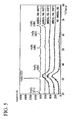
- an annealing process was performed on the amorphous IZO film formed on the glass substrate at a temperature in the range of 300°C to 800°C in a N 2 atmosphere for one minute, and then the state of the IZO film after the annealing process was measured by an X-ray diffraction (XRD) method. The measured results are shown in FIG. 5 .
- FIG. 5 is a graph illustrating the X-ray diffraction (XRD) results of the IZO film, in which the horizontal axis indicates a diffraction angle (2 ⁇ (°)) and the vertical axis indicates analysis strength.
- XRD X-ray diffraction
- the annealing process is performed on the IZO film at a temperature of 600°C or more, the peak of X-rays composed of In 2 O 3 is mainly detected, and the IZO film is crystallized.
- the annealing process is performed on the IZO film at a temperature of 400°C or less, the IZO film is not crystallized.
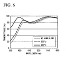
- UV-visible spectrophotometer (UV-2450 manufactured by Shimadze Corporation) was used to measure the transmittance of the IZO film.
- the transmittance value was obtained by subtracting the blank value of the transmittance of a glass substrate.
- FIG. 6 is a graph illustrating the transmittance of the IZO film, in which the horizontal axis indicates a wavelength (nm) and the vertical axis indicates the transmittance (%).
- the transmittance of the IZO film in an ultraviolet range (350 nm to 420 nm) is 20 to 30% higher than that of the IZO film not subjected to the annealing process.
- the gallium nitride compound semiconductor layer 20 shown in FIG. 3 was manufactured as follows.
- the layers 22 to 27 of the laminated structure of the gallium nitride compound semiconductor layer 20 were grown by a general low pressure MOCVD device.
- the gallium nitride compound semiconductor layer 20 shown in FIG. 3 was used to manufacture a gallium nitride compound semiconductor light-emitting device.
- HF and HCl were used to clean the surface of the p-type GaN contact layer 27 of the gallium nitride compound semiconductor layer 20, and an IZO film was formed with a thickness of 220 nm on the p-type GaN contact layer 27 by a DC magnetron sputter.
- an IZO target having an IZO concentration of 10% by mass was used.
- the IZO film was formed under the conditions of an Ar flow rate of 70 sccm and a pressure of about 0.3 Pa.
- the IZO film manufactured by the above-mentioned method had a transmittance of about 60% in a wavelength range of about 400 nm, and the sheet resistance thereof was 17 ⁇ /sq.
- an X-ray diffraction (XRD) method was used to measure the state of the IZO film formed by the above-mentioned method, and the result proved that the IZO film was in an amorphous state.
- the amorphous IZO film was patterned by a photolithography technique and wet etching such that the IZO film was formed only on a region for forming a positive electrode of the p-type GaN contact layer 27.
- the amorphous IZO film was etched at an etching rate of about 40 nm/min.
- the IZO film was annealed in an RTA annealing furnace in a N 2 gas atmosphere at a temperature of 600°C for one minute.
- the IZO film subjected to the annealing process had high transmittance in a wavelength range of about 400 nm and a transmittance of 90% or more in a wavelength range of 400 nm.
- the sheet resistance of the IZO film was 14 ⁇ /sq.
- an X-ray diffraction (XRD) method was used to measure the state of the IZO film, and the measured results showed that the peak of X-rays composed of In 2 O 3 was mainly detected and the IZO film was crystallized.
- etching was performed on a region for forming an n-type electrode to expose the surface of the Si-doped n-type GaN contact layer 23 only in the region.
- the rear surface of the substrate 11 formed of sapphire was polished into a mirror surface by polishing particles, such as diamond particles.
- the laminated structure was cut into individual square chips each having a 350 ⁇ m square, thereby obtaining a semiconductor light-emitting device.
- the manufactured semiconductor light-emitting device (chip) was mounted to the lead frame, and then connected to the lead frame by gold (Au) lines. Then, a probe contacted the chip and a current of 20 mA was applied to the semiconductor light-emitting device to measure a forward voltage (driving voltage: Vf). In addition, the emission power Po and the emission wavelength were measured by a general integrating sphere.
- the semiconductor light-emitting device had an emission wavelength in a wavelength range of about 400 nm, and the driving voltage Vf and the emission power Po of the semiconductor light-emitting device were 3.3 V and 15 mW, respectively.
- a semiconductor light-emitting device was manufactured, similar to Comparative Example 1, except that a mixed gas of N 2 and H 2 was used for an annealing process.
- the IZO film immediately after the annealing process had a transmittance of 90% or more in a wavelength range of about 400 nm and a sheet resistance of 11 ⁇ /sq.
- the obtained semiconductor light-emitting device had an emission wavelength in the wavelength range of about 400 nm, and the driving voltage Vf and the emission power Po of the semiconductor light-emitting device were 3.25 V and 15 mW, respectively.
- a semiconductor light-emitting device was manufactured, similar to Comparative Example 1, except that an annealing process was performed at a temperature of 300°C.
- the IZO film after the annealing process had a transmittance of about 70% in a wavelength range of about 400 nm and a sheet resistance of 16 ⁇ /sq.
- the obtained semiconductor light-emitting device had an emission wavelength in the wavelength range of about 400 nm, and the driving voltage Vf and the emission power Po of the semiconductor light-emitting device were 3.3 V and 12 mW, respectively.
- an ITO film with a thickness of 250 nm was formed on the p-type GaN contact layer 27 of the gallium nitride compound semiconductor layer 20 by a sputtering method. Then, wet etching was performed on the amorphous IZO film using a liquid mixture of FeCl 3 and HCl to form the IZO film only on a region for forming a positive electrode of the p-type GaN contact layer 27. After patterning the IZO film, a two-stage annealing process was performed on the IZO film.
- an annealing process was performed on the IZO film in a N 2 gas atmosphere including 25% of O 2 at a temperature of 600°C for one minute, and then another annealing process was performed on the IZO film in a N 2 atmosphere at a temperature of 500°C for one minute.
- the IZO film after the two-stage annealing process had a transmittance of about 80% in a wavelength range of about 400 nm and a sheet resistance of 15 ⁇ /sq.
- a semiconductor light-emitting device was manufactured, similar to Comparative Example 1.
- the obtained semiconductor light-emitting device had an emission wavelength in the wavelength range of about 400 nm, and the driving voltage Vf and the emission power Po of the semiconductor light-emitting device were 3.3 V and 13 mW, respectively.
- Example 1 and Comparative examples 1 to 3 showed that, in the semiconductor light-emitting devices according to Comparative Example 1 and Example 1 in which the annealing process was performed on the IZO film forming the positive electrode, the IZO film had higher transmittance and lower sheet resistance than that in the semiconductor light-emitting devices according to Comparative example 2 and Comparative example 3.
- the IZO film had also a lower sheet resistance than that in the semiconductor light-emitting device of Comparative Example 1.
- the emission power Po of light in the ultraviolet range was higher than that in the semiconductor light-emitting devices according to Comparative examples 2 and 3.
- the present invention can be applied to a method of manufacturing a semiconductor light-emitting device. Particular, the present invention can be applied to a method of manufacturing a semiconductor light-emitting device having high emission power Po of ultraviolet light
Applications Claiming Priority (2)
| Application Number | Priority Date | Filing Date | Title |
|---|---|---|---|
| JP2006112012A JP5265090B2 (ja) | 2006-04-14 | 2006-04-14 | 半導体発光素子およびランプ |
| PCT/JP2007/058193 WO2007119830A1 (ja) | 2006-04-14 | 2007-04-13 | 半導体発光素子、半導体発光素子の製造方法およびランプ |
Publications (3)
| Publication Number | Publication Date |
|---|---|
| EP2012371A1 EP2012371A1 (en) | 2009-01-07 |
| EP2012371A4 EP2012371A4 (en) | 2014-01-22 |
| EP2012371B1 true EP2012371B1 (en) | 2015-02-25 |
Family
ID=38609590
Family Applications (1)
| Application Number | Title | Priority Date | Filing Date |
|---|---|---|---|
| EP07741629.5A Active EP2012371B1 (en) | 2006-04-14 | 2007-04-13 | Method for fabricating a semiconductor light emitting device |
Country Status (7)
| Country | Link |
|---|---|
| US (1) | US8334200B2 (ja) |
| EP (1) | EP2012371B1 (ja) |
| JP (1) | JP5265090B2 (ja) |
| KR (1) | KR100988143B1 (ja) |
| CN (1) | CN101421856A (ja) |
| TW (1) | TWI359509B (ja) |
| WO (1) | WO2007119830A1 (ja) |
Families Citing this family (18)
| Publication number | Priority date | Publication date | Assignee | Title |
|---|---|---|---|---|
| JP5201566B2 (ja) * | 2006-12-11 | 2013-06-05 | 豊田合成株式会社 | 化合物半導体発光素子及びその製造方法 |
| JPWO2008081566A1 (ja) | 2006-12-28 | 2010-04-30 | 日本電気株式会社 | 電極構造、半導体素子、およびそれらの製造方法 |
| US20080223434A1 (en) * | 2007-02-19 | 2008-09-18 | Showa Denko K.K. | Solar cell and process for producing the same |
| JP2009260237A (ja) * | 2008-01-24 | 2009-11-05 | Showa Denko Kk | 化合物半導体発光素子及びその製造方法、化合物半導体発光素子用導電型透光性電極、ランプ、電子機器並びに機械装置 |
| JP5520496B2 (ja) * | 2008-02-19 | 2014-06-11 | 昭和電工株式会社 | 太陽電池の製造方法 |
| KR101481855B1 (ko) * | 2008-03-06 | 2015-01-12 | 스미토모 긴조쿠 고잔 가부시키가이샤 | 반도체 발광소자, 반도체 발광소자의 제조방법 및 이 반도체 발광소자를 사용한 램프 |
| JP5522032B2 (ja) * | 2008-03-13 | 2014-06-18 | 豊田合成株式会社 | 半導体発光素子及びその製造方法 |
| JP5083973B2 (ja) * | 2008-03-28 | 2012-11-28 | スタンレー電気株式会社 | 光半導体素子の製造方法 |
| JP2009246275A (ja) * | 2008-03-31 | 2009-10-22 | Showa Denko Kk | Iii族窒化物半導体発光素子及びランプ |
| JP2009253056A (ja) * | 2008-04-07 | 2009-10-29 | Showa Denko Kk | Iii族窒化物半導体発光素子及びランプ |
| JP2009283551A (ja) * | 2008-05-20 | 2009-12-03 | Showa Denko Kk | 半導体発光素子及びその製造方法、ランプ |
| JP2011086855A (ja) * | 2009-10-19 | 2011-04-28 | Showa Denko Kk | 半導体発光素子の製造方法 |
| JP5379703B2 (ja) * | 2010-01-26 | 2013-12-25 | パナソニック株式会社 | 紫外半導体発光素子 |
| US20110244663A1 (en) * | 2010-04-01 | 2011-10-06 | Applied Materials, Inc. | Forming a compound-nitride structure that includes a nucleation layer |
| CN101847677B (zh) * | 2010-04-07 | 2012-11-14 | 中国科学院半导体研究所 | 采用mvpe两步法制备氧化锌透明电极的方法 |
| JP5829014B2 (ja) * | 2010-09-30 | 2015-12-09 | シャープ株式会社 | 化合物半導体発光素子の製造方法 |
| CN110459658A (zh) * | 2018-05-08 | 2019-11-15 | 山东浪潮华光光电子股份有限公司 | 一种P型GaN层的UV LED芯片及其制备方法 |
| CN112420888B (zh) * | 2021-01-21 | 2021-04-23 | 华灿光电(浙江)有限公司 | 紫外发光二极管外延片及其制备方法 |
Family Cites Families (15)
| Publication number | Priority date | Publication date | Assignee | Title |
|---|---|---|---|---|
| JPS6222312A (ja) * | 1985-07-23 | 1987-01-30 | アルプス電気株式会社 | 透明導電性被膜の形成方法 |
| JPH05299175A (ja) | 1992-04-24 | 1993-11-12 | Fuji Xerox Co Ltd | El発光素子 |
| JP2000026119A (ja) | 1998-07-09 | 2000-01-25 | Hoya Corp | 透明導電性酸化物薄膜を有する物品及びその製造方法 |
| JP2000067657A (ja) * | 1998-08-26 | 2000-03-03 | Internatl Business Mach Corp <Ibm> | 赤外線透過に優れた透明導電膜及びその製造方法 |
| CN1195886C (zh) * | 1999-11-25 | 2005-04-06 | 出光兴产株式会社 | 溅射靶、透明导电氧化物和制备该溅射靶的方法 |
| JP2002164570A (ja) * | 2000-11-24 | 2002-06-07 | Shiro Sakai | 窒化ガリウム系化合物半導体装置 |
| JP4310984B2 (ja) * | 2002-02-06 | 2009-08-12 | 株式会社日立製作所 | 有機発光表示装置 |
| JP3720341B2 (ja) * | 2003-02-12 | 2005-11-24 | ローム株式会社 | 半導体発光素子 |
| JP4259268B2 (ja) | 2003-10-20 | 2009-04-30 | 豊田合成株式会社 | 半導体発光素子 |
| JP2005217331A (ja) * | 2004-01-30 | 2005-08-11 | Nichia Chem Ind Ltd | 半導体発光素子 |
| JP2005259891A (ja) * | 2004-03-10 | 2005-09-22 | Toyoda Gosei Co Ltd | 発光装置 |
| KR100634503B1 (ko) * | 2004-03-12 | 2006-10-16 | 삼성전자주식회사 | 질화물계 발광소자 및 그 제조방법 |
| US7339255B2 (en) * | 2004-08-24 | 2008-03-04 | Kabushiki Kaisha Toshiba | Semiconductor device having bidirectionally inclined toward <1-100> and <11-20> relative to {0001} crystal planes |
| US8728615B2 (en) * | 2004-09-13 | 2014-05-20 | Sumitomo Metal Mining Co., Ltd. | Transparent conductive film and method of fabricating the same, transparent conductive base material, and light-emitting device |
| JP4578929B2 (ja) | 2004-10-15 | 2010-11-10 | 日本エステル株式会社 | ポリ乳酸系複合バインダー繊維 |
-
2006
- 2006-04-14 JP JP2006112012A patent/JP5265090B2/ja active Active
-
2007
- 2007-04-13 US US12/296,849 patent/US8334200B2/en active Active
- 2007-04-13 EP EP07741629.5A patent/EP2012371B1/en active Active
- 2007-04-13 WO PCT/JP2007/058193 patent/WO2007119830A1/ja active Application Filing
- 2007-04-13 KR KR1020087024670A patent/KR100988143B1/ko active IP Right Grant
- 2007-04-13 CN CNA2007800128677A patent/CN101421856A/zh active Pending
- 2007-04-14 TW TW096113231A patent/TWI359509B/zh active
Also Published As
| Publication number | Publication date |
|---|---|
| WO2007119830A1 (ja) | 2007-10-25 |
| JP5265090B2 (ja) | 2013-08-14 |
| US8334200B2 (en) | 2012-12-18 |
| EP2012371A4 (en) | 2014-01-22 |
| TWI359509B (en) | 2012-03-01 |
| US20090179220A1 (en) | 2009-07-16 |
| KR20080104363A (ko) | 2008-12-02 |
| EP2012371A1 (en) | 2009-01-07 |
| TW200805714A (en) | 2008-01-16 |
| KR100988143B1 (ko) | 2010-10-18 |
| JP2007287845A (ja) | 2007-11-01 |
| CN101421856A (zh) | 2009-04-29 |
Similar Documents
| Publication | Publication Date | Title |
|---|---|---|
| EP2012371B1 (en) | Method for fabricating a semiconductor light emitting device | |
| EP2012370B1 (en) | Method for manufacturing semiconductor light emitting element, semiconductor light emitting element and lamp provided with the semiconductor light emitting element | |
| US7972952B2 (en) | Compound semiconductor light-emitting device and method for manufacturing the same | |
| EP2012372B1 (en) | Method for manufacturing gallium nitride compound semiconductor light emitting element | |
| EP1998381B1 (en) | Method for manufacturing gallium nitride compound semiconductor light-emitting device and lamp using same | |
| US8222667B2 (en) | Semiconductor light-emitting element, method for manufacturing the semiconductor light-emitting element and lamp that uses the semiconductor light-emitting element | |
| US7498611B2 (en) | Transparent electrode for semiconductor light-emitting device | |
| US7888687B2 (en) | Electrode for semiconductor light emitting device | |
| US7875896B2 (en) | Transparent positive electrode | |
| JP4252622B1 (ja) | 半導体発光素子の製造方法 |
Legal Events
| Date | Code | Title | Description |
|---|---|---|---|
| PUAI | Public reference made under article 153(3) epc to a published international application that has entered the european phase |
Free format text: ORIGINAL CODE: 0009012 |
|
| 17P | Request for examination filed |
Effective date: 20081112 |
|
| AK | Designated contracting states |
Kind code of ref document: A1 Designated state(s): AT BE BG CH CY CZ DE DK EE ES FI FR GB GR HU IE IS IT LI LT LU LV MC MT NL PL PT RO SE SI SK TR |
|
| AX | Request for extension of the european patent |
Extension state: AL BA HR MK RS |
|
| DAX | Request for extension of the european patent (deleted) | ||
| RAP1 | Party data changed (applicant data changed or rights of an application transferred) |
Owner name: TOYODA GOSEI CO., LTD. |
|
| A4 | Supplementary search report drawn up and despatched |
Effective date: 20131220 |
|
| RIC1 | Information provided on ipc code assigned before grant |
Ipc: H01L 33/32 20100101ALI20131216BHEP Ipc: H01L 33/42 20100101ALI20131216BHEP Ipc: H01L 33/00 20100101AFI20131216BHEP |
|
| 17Q | First examination report despatched |
Effective date: 20140117 |
|
| GRAP | Despatch of communication of intention to grant a patent |
Free format text: ORIGINAL CODE: EPIDOSNIGR1 |
|
| INTG | Intention to grant announced |
Effective date: 20140929 |
|
| RIN1 | Information on inventor provided before grant (corrected) |
Inventor name: FUKUNAGA, NAOKI Inventor name: OSAWA, HIROSHI |
|
| GRAS | Grant fee paid |
Free format text: ORIGINAL CODE: EPIDOSNIGR3 |
|
| GRAA | (expected) grant |
Free format text: ORIGINAL CODE: 0009210 |
|
| AK | Designated contracting states |
Kind code of ref document: B1 Designated state(s): AT BE BG CH CY CZ DE DK EE ES FI FR GB GR HU IE IS IT LI LT LU LV MC MT NL PL PT RO SE SI SK TR |
|
| REG | Reference to a national code |
Ref country code: GB Ref legal event code: FG4D |
|
| REG | Reference to a national code |
Ref country code: CH Ref legal event code: EP |
|
| REG | Reference to a national code |
Ref country code: IE Ref legal event code: FG4D |
|
| REG | Reference to a national code |
Ref country code: DE Ref legal event code: R096 Ref document number: 602007040347 Country of ref document: DE Effective date: 20150409 |
|
| REG | Reference to a national code |
Ref country code: AT Ref legal event code: REF Ref document number: 712640 Country of ref document: AT Kind code of ref document: T Effective date: 20150415 |
|
| REG | Reference to a national code |
Ref country code: NL Ref legal event code: VDEP Effective date: 20150225 |
|
| REG | Reference to a national code |
Ref country code: AT Ref legal event code: MK05 Ref document number: 712640 Country of ref document: AT Kind code of ref document: T Effective date: 20150225 |
|
| REG | Reference to a national code |
Ref country code: LT Ref legal event code: MG4D |
|
| PG25 | Lapsed in a contracting state [announced via postgrant information from national office to epo] |
Ref country code: LT Free format text: LAPSE BECAUSE OF FAILURE TO SUBMIT A TRANSLATION OF THE DESCRIPTION OR TO PAY THE FEE WITHIN THE PRESCRIBED TIME-LIMIT Effective date: 20150225 Ref country code: FI Free format text: LAPSE BECAUSE OF FAILURE TO SUBMIT A TRANSLATION OF THE DESCRIPTION OR TO PAY THE FEE WITHIN THE PRESCRIBED TIME-LIMIT Effective date: 20150225 Ref country code: SE Free format text: LAPSE BECAUSE OF FAILURE TO SUBMIT A TRANSLATION OF THE DESCRIPTION OR TO PAY THE FEE WITHIN THE PRESCRIBED TIME-LIMIT Effective date: 20150225 Ref country code: ES Free format text: LAPSE BECAUSE OF FAILURE TO SUBMIT A TRANSLATION OF THE DESCRIPTION OR TO PAY THE FEE WITHIN THE PRESCRIBED TIME-LIMIT Effective date: 20150225 |
|
| PG25 | Lapsed in a contracting state [announced via postgrant information from national office to epo] |
Ref country code: GR Free format text: LAPSE BECAUSE OF FAILURE TO SUBMIT A TRANSLATION OF THE DESCRIPTION OR TO PAY THE FEE WITHIN THE PRESCRIBED TIME-LIMIT Effective date: 20150526 Ref country code: LV Free format text: LAPSE BECAUSE OF FAILURE TO SUBMIT A TRANSLATION OF THE DESCRIPTION OR TO PAY THE FEE WITHIN THE PRESCRIBED TIME-LIMIT Effective date: 20150225 Ref country code: AT Free format text: LAPSE BECAUSE OF FAILURE TO SUBMIT A TRANSLATION OF THE DESCRIPTION OR TO PAY THE FEE WITHIN THE PRESCRIBED TIME-LIMIT Effective date: 20150225 Ref country code: IS Free format text: LAPSE BECAUSE OF FAILURE TO SUBMIT A TRANSLATION OF THE DESCRIPTION OR TO PAY THE FEE WITHIN THE PRESCRIBED TIME-LIMIT Effective date: 20150625 |
|
| PG25 | Lapsed in a contracting state [announced via postgrant information from national office to epo] |
Ref country code: NL Free format text: LAPSE BECAUSE OF FAILURE TO SUBMIT A TRANSLATION OF THE DESCRIPTION OR TO PAY THE FEE WITHIN THE PRESCRIBED TIME-LIMIT Effective date: 20150225 |
|
| PG25 | Lapsed in a contracting state [announced via postgrant information from national office to epo] |
Ref country code: EE Free format text: LAPSE BECAUSE OF FAILURE TO SUBMIT A TRANSLATION OF THE DESCRIPTION OR TO PAY THE FEE WITHIN THE PRESCRIBED TIME-LIMIT Effective date: 20150225 Ref country code: SK Free format text: LAPSE BECAUSE OF FAILURE TO SUBMIT A TRANSLATION OF THE DESCRIPTION OR TO PAY THE FEE WITHIN THE PRESCRIBED TIME-LIMIT Effective date: 20150225 Ref country code: CZ Free format text: LAPSE BECAUSE OF FAILURE TO SUBMIT A TRANSLATION OF THE DESCRIPTION OR TO PAY THE FEE WITHIN THE PRESCRIBED TIME-LIMIT Effective date: 20150225 Ref country code: DK Free format text: LAPSE BECAUSE OF FAILURE TO SUBMIT A TRANSLATION OF THE DESCRIPTION OR TO PAY THE FEE WITHIN THE PRESCRIBED TIME-LIMIT Effective date: 20150225 Ref country code: RO Free format text: LAPSE BECAUSE OF FAILURE TO SUBMIT A TRANSLATION OF THE DESCRIPTION OR TO PAY THE FEE WITHIN THE PRESCRIBED TIME-LIMIT Effective date: 20150225 |
|
| REG | Reference to a national code |
Ref country code: DE Ref legal event code: R097 Ref document number: 602007040347 Country of ref document: DE |
|
| PG25 | Lapsed in a contracting state [announced via postgrant information from national office to epo] |
Ref country code: PL Free format text: LAPSE BECAUSE OF FAILURE TO SUBMIT A TRANSLATION OF THE DESCRIPTION OR TO PAY THE FEE WITHIN THE PRESCRIBED TIME-LIMIT Effective date: 20150225 Ref country code: MC Free format text: LAPSE BECAUSE OF FAILURE TO SUBMIT A TRANSLATION OF THE DESCRIPTION OR TO PAY THE FEE WITHIN THE PRESCRIBED TIME-LIMIT Effective date: 20150225 Ref country code: LU Free format text: LAPSE BECAUSE OF FAILURE TO SUBMIT A TRANSLATION OF THE DESCRIPTION OR TO PAY THE FEE WITHIN THE PRESCRIBED TIME-LIMIT Effective date: 20150413 |
|
| REG | Reference to a national code |
Ref country code: CH Ref legal event code: PL |
|
| PG25 | Lapsed in a contracting state [announced via postgrant information from national office to epo] |
Ref country code: IT Free format text: LAPSE BECAUSE OF FAILURE TO SUBMIT A TRANSLATION OF THE DESCRIPTION OR TO PAY THE FEE WITHIN THE PRESCRIBED TIME-LIMIT Effective date: 20150225 |
|
| PLBE | No opposition filed within time limit |
Free format text: ORIGINAL CODE: 0009261 |
|
| STAA | Information on the status of an ep patent application or granted ep patent |
Free format text: STATUS: NO OPPOSITION FILED WITHIN TIME LIMIT |
|
| GBPC | Gb: european patent ceased through non-payment of renewal fee |
Effective date: 20150525 |
|
| REG | Reference to a national code |
Ref country code: IE Ref legal event code: MM4A |
|
| PG25 | Lapsed in a contracting state [announced via postgrant information from national office to epo] |
Ref country code: CH Free format text: LAPSE BECAUSE OF NON-PAYMENT OF DUE FEES Effective date: 20150430 Ref country code: LI Free format text: LAPSE BECAUSE OF NON-PAYMENT OF DUE FEES Effective date: 20150430 |
|
| REG | Reference to a national code |
Ref country code: FR Ref legal event code: ST Effective date: 20151231 |
|
| 26N | No opposition filed |
Effective date: 20151126 |
|
| PG25 | Lapsed in a contracting state [announced via postgrant information from national office to epo] |
Ref country code: FR Free format text: LAPSE BECAUSE OF NON-PAYMENT OF DUE FEES Effective date: 20150430 Ref country code: SI Free format text: LAPSE BECAUSE OF FAILURE TO SUBMIT A TRANSLATION OF THE DESCRIPTION OR TO PAY THE FEE WITHIN THE PRESCRIBED TIME-LIMIT Effective date: 20150225 |
|
| PG25 | Lapsed in a contracting state [announced via postgrant information from national office to epo] |
Ref country code: GB Free format text: LAPSE BECAUSE OF NON-PAYMENT OF DUE FEES Effective date: 20150525 Ref country code: IE Free format text: LAPSE BECAUSE OF NON-PAYMENT OF DUE FEES Effective date: 20150413 |
|
| PG25 | Lapsed in a contracting state [announced via postgrant information from national office to epo] |
Ref country code: BE Free format text: LAPSE BECAUSE OF FAILURE TO SUBMIT A TRANSLATION OF THE DESCRIPTION OR TO PAY THE FEE WITHIN THE PRESCRIBED TIME-LIMIT Effective date: 20150225 |
|
| PG25 | Lapsed in a contracting state [announced via postgrant information from national office to epo] |
Ref country code: MT Free format text: LAPSE BECAUSE OF FAILURE TO SUBMIT A TRANSLATION OF THE DESCRIPTION OR TO PAY THE FEE WITHIN THE PRESCRIBED TIME-LIMIT Effective date: 20150225 |
|
| PG25 | Lapsed in a contracting state [announced via postgrant information from national office to epo] |
Ref country code: HU Free format text: LAPSE BECAUSE OF FAILURE TO SUBMIT A TRANSLATION OF THE DESCRIPTION OR TO PAY THE FEE WITHIN THE PRESCRIBED TIME-LIMIT; INVALID AB INITIO Effective date: 20070413 Ref country code: BG Free format text: LAPSE BECAUSE OF FAILURE TO SUBMIT A TRANSLATION OF THE DESCRIPTION OR TO PAY THE FEE WITHIN THE PRESCRIBED TIME-LIMIT Effective date: 20150225 |
|
| PG25 | Lapsed in a contracting state [announced via postgrant information from national office to epo] |
Ref country code: CY Free format text: LAPSE BECAUSE OF FAILURE TO SUBMIT A TRANSLATION OF THE DESCRIPTION OR TO PAY THE FEE WITHIN THE PRESCRIBED TIME-LIMIT Effective date: 20150225 |
|
| PG25 | Lapsed in a contracting state [announced via postgrant information from national office to epo] |
Ref country code: PT Free format text: LAPSE BECAUSE OF FAILURE TO SUBMIT A TRANSLATION OF THE DESCRIPTION OR TO PAY THE FEE WITHIN THE PRESCRIBED TIME-LIMIT Effective date: 20150625 |
|
| PG25 | Lapsed in a contracting state [announced via postgrant information from national office to epo] |
Ref country code: TR Free format text: LAPSE BECAUSE OF FAILURE TO SUBMIT A TRANSLATION OF THE DESCRIPTION OR TO PAY THE FEE WITHIN THE PRESCRIBED TIME-LIMIT Effective date: 20150225 |
|
| PGFP | Annual fee paid to national office [announced via postgrant information from national office to epo] |
Ref country code: DE Payment date: 20230228 Year of fee payment: 17 |