EP1944118B1 - Procédé de traitement laser - Google Patents
Procédé de traitement laser Download PDFInfo
- Publication number
- EP1944118B1 EP1944118B1 EP06797913.8A EP06797913A EP1944118B1 EP 1944118 B1 EP1944118 B1 EP 1944118B1 EP 06797913 A EP06797913 A EP 06797913A EP 1944118 B1 EP1944118 B1 EP 1944118B1
- Authority
- EP
- European Patent Office
- Prior art keywords
- cut
- laser light
- line
- region
- modified region
- Prior art date
- Legal status (The legal status is an assumption and is not a legal conclusion. Google has not performed a legal analysis and makes no representation as to the accuracy of the status listed.)
- Active
Links
- 238000003672 processing method Methods 0.000 title claims description 36
- 238000005520 cutting process Methods 0.000 claims description 58
- 239000000758 substrate Substances 0.000 claims description 21
- 239000004065 semiconductor Substances 0.000 claims description 14
- 238000009826 distribution Methods 0.000 claims description 7
- 230000001678 irradiating effect Effects 0.000 claims description 2
- XUIMIQQOPSSXEZ-UHFFFAOYSA-N Silicon Chemical compound [Si] XUIMIQQOPSSXEZ-UHFFFAOYSA-N 0.000 description 41
- 229910052710 silicon Inorganic materials 0.000 description 40
- 239000010703 silicon Substances 0.000 description 40
- 101100008049 Caenorhabditis elegans cut-5 gene Proteins 0.000 description 36
- 238000010521 absorption reaction Methods 0.000 description 25
- 230000003287 optical effect Effects 0.000 description 9
- 238000002834 transmittance Methods 0.000 description 6
- 238000003776 cleavage reaction Methods 0.000 description 5
- 238000002474 experimental method Methods 0.000 description 5
- 239000011521 glass Substances 0.000 description 5
- 239000000463 material Substances 0.000 description 5
- 238000000034 method Methods 0.000 description 5
- 230000007017 scission Effects 0.000 description 5
- 239000013078 crystal Substances 0.000 description 4
- 210000000887 face Anatomy 0.000 description 3
- 238000010438 heat treatment Methods 0.000 description 3
- 230000010287 polarization Effects 0.000 description 3
- 230000000694 effects Effects 0.000 description 2
- 230000002349 favourable effect Effects 0.000 description 2
- 238000003913 materials processing Methods 0.000 description 2
- 230000010355 oscillation Effects 0.000 description 2
- 238000005086 pumping Methods 0.000 description 2
- 238000007493 shaping process Methods 0.000 description 2
- 230000035882 stress Effects 0.000 description 2
- RZVAJINKPMORJF-UHFFFAOYSA-N Acetaminophen Chemical compound CC(=O)NC1=CC=C(O)C=C1 RZVAJINKPMORJF-UHFFFAOYSA-N 0.000 description 1
- 229910001218 Gallium arsenide Inorganic materials 0.000 description 1
- 229910012463 LiTaO3 Inorganic materials 0.000 description 1
- 229910021417 amorphous silicon Inorganic materials 0.000 description 1
- 238000005452 bending Methods 0.000 description 1
- 150000001875 compounds Chemical class 0.000 description 1
- 238000005336 cracking Methods 0.000 description 1
- 238000002425 crystallisation Methods 0.000 description 1
- 230000008025 crystallization Effects 0.000 description 1
- 230000002542 deteriorative effect Effects 0.000 description 1
- 229910003460 diamond Inorganic materials 0.000 description 1
- 239000010432 diamond Substances 0.000 description 1
- 238000011156 evaluation Methods 0.000 description 1
- 230000031700 light absorption Effects 0.000 description 1
- 239000011159 matrix material Substances 0.000 description 1
- TWNQGVIAIRXVLR-UHFFFAOYSA-N oxo(oxoalumanyloxy)alumane Chemical compound O=[Al]O[Al]=O TWNQGVIAIRXVLR-UHFFFAOYSA-N 0.000 description 1
- 210000001747 pupil Anatomy 0.000 description 1
- 239000005297 pyrex Substances 0.000 description 1
- 238000000926 separation method Methods 0.000 description 1
- 229910052950 sphalerite Inorganic materials 0.000 description 1
- 230000008646 thermal stress Effects 0.000 description 1
- 238000003466 welding Methods 0.000 description 1
Images


Classifications
-
- B—PERFORMING OPERATIONS; TRANSPORTING
- B23—MACHINE TOOLS; METAL-WORKING NOT OTHERWISE PROVIDED FOR
- B23K—SOLDERING OR UNSOLDERING; WELDING; CLADDING OR PLATING BY SOLDERING OR WELDING; CUTTING BY APPLYING HEAT LOCALLY, e.g. FLAME CUTTING; WORKING BY LASER BEAM
- B23K26/00—Working by laser beam, e.g. welding, cutting or boring
- B23K26/36—Removing material
- B23K26/38—Removing material by boring or cutting
-
- B—PERFORMING OPERATIONS; TRANSPORTING
- B28—WORKING CEMENT, CLAY, OR STONE
- B28D—WORKING STONE OR STONE-LIKE MATERIALS
- B28D5/00—Fine working of gems, jewels, crystals, e.g. of semiconductor material; apparatus or devices therefor
-
- B—PERFORMING OPERATIONS; TRANSPORTING
- B23—MACHINE TOOLS; METAL-WORKING NOT OTHERWISE PROVIDED FOR
- B23K—SOLDERING OR UNSOLDERING; WELDING; CLADDING OR PLATING BY SOLDERING OR WELDING; CUTTING BY APPLYING HEAT LOCALLY, e.g. FLAME CUTTING; WORKING BY LASER BEAM
- B23K26/00—Working by laser beam, e.g. welding, cutting or boring
- B23K26/02—Positioning or observing the workpiece, e.g. with respect to the point of impact; Aligning, aiming or focusing the laser beam
- B23K26/06—Shaping the laser beam, e.g. by masks or multi-focusing
- B23K26/062—Shaping the laser beam, e.g. by masks or multi-focusing by direct control of the laser beam
-
- B—PERFORMING OPERATIONS; TRANSPORTING
- B23—MACHINE TOOLS; METAL-WORKING NOT OTHERWISE PROVIDED FOR
- B23K—SOLDERING OR UNSOLDERING; WELDING; CLADDING OR PLATING BY SOLDERING OR WELDING; CUTTING BY APPLYING HEAT LOCALLY, e.g. FLAME CUTTING; WORKING BY LASER BEAM
- B23K26/00—Working by laser beam, e.g. welding, cutting or boring
- B23K26/02—Positioning or observing the workpiece, e.g. with respect to the point of impact; Aligning, aiming or focusing the laser beam
- B23K26/06—Shaping the laser beam, e.g. by masks or multi-focusing
- B23K26/064—Shaping the laser beam, e.g. by masks or multi-focusing by means of optical elements, e.g. lenses, mirrors or prisms
- B23K26/066—Shaping the laser beam, e.g. by masks or multi-focusing by means of optical elements, e.g. lenses, mirrors or prisms by using masks
-
- B—PERFORMING OPERATIONS; TRANSPORTING
- B23—MACHINE TOOLS; METAL-WORKING NOT OTHERWISE PROVIDED FOR
- B23K—SOLDERING OR UNSOLDERING; WELDING; CLADDING OR PLATING BY SOLDERING OR WELDING; CUTTING BY APPLYING HEAT LOCALLY, e.g. FLAME CUTTING; WORKING BY LASER BEAM
- B23K26/00—Working by laser beam, e.g. welding, cutting or boring
- B23K26/02—Positioning or observing the workpiece, e.g. with respect to the point of impact; Aligning, aiming or focusing the laser beam
- B23K26/06—Shaping the laser beam, e.g. by masks or multi-focusing
- B23K26/073—Shaping the laser spot
-
- B—PERFORMING OPERATIONS; TRANSPORTING
- B23—MACHINE TOOLS; METAL-WORKING NOT OTHERWISE PROVIDED FOR
- B23K—SOLDERING OR UNSOLDERING; WELDING; CLADDING OR PLATING BY SOLDERING OR WELDING; CUTTING BY APPLYING HEAT LOCALLY, e.g. FLAME CUTTING; WORKING BY LASER BEAM
- B23K26/00—Working by laser beam, e.g. welding, cutting or boring
- B23K26/36—Removing material
- B23K26/40—Removing material taking account of the properties of the material involved
-
- B—PERFORMING OPERATIONS; TRANSPORTING
- B23—MACHINE TOOLS; METAL-WORKING NOT OTHERWISE PROVIDED FOR
- B23K—SOLDERING OR UNSOLDERING; WELDING; CLADDING OR PLATING BY SOLDERING OR WELDING; CUTTING BY APPLYING HEAT LOCALLY, e.g. FLAME CUTTING; WORKING BY LASER BEAM
- B23K26/00—Working by laser beam, e.g. welding, cutting or boring
- B23K26/50—Working by transmitting the laser beam through or within the workpiece
- B23K26/53—Working by transmitting the laser beam through or within the workpiece for modifying or reforming the material inside the workpiece, e.g. for producing break initiation cracks
-
- H—ELECTRICITY
- H01—ELECTRIC ELEMENTS
- H01L—SEMICONDUCTOR DEVICES NOT COVERED BY CLASS H10
- H01L21/00—Processes or apparatus adapted for the manufacture or treatment of semiconductor or solid state devices or of parts thereof
- H01L21/70—Manufacture or treatment of devices consisting of a plurality of solid state components formed in or on a common substrate or of parts thereof; Manufacture of integrated circuit devices or of parts thereof
- H01L21/77—Manufacture or treatment of devices consisting of a plurality of solid state components or integrated circuits formed in, or on, a common substrate
- H01L21/78—Manufacture or treatment of devices consisting of a plurality of solid state components or integrated circuits formed in, or on, a common substrate with subsequent division of the substrate into plural individual devices
-
- B—PERFORMING OPERATIONS; TRANSPORTING
- B23—MACHINE TOOLS; METAL-WORKING NOT OTHERWISE PROVIDED FOR
- B23K—SOLDERING OR UNSOLDERING; WELDING; CLADDING OR PLATING BY SOLDERING OR WELDING; CUTTING BY APPLYING HEAT LOCALLY, e.g. FLAME CUTTING; WORKING BY LASER BEAM
- B23K2101/00—Articles made by soldering, welding or cutting
- B23K2101/36—Electric or electronic devices
- B23K2101/40—Semiconductor devices
-
- B—PERFORMING OPERATIONS; TRANSPORTING
- B23—MACHINE TOOLS; METAL-WORKING NOT OTHERWISE PROVIDED FOR
- B23K—SOLDERING OR UNSOLDERING; WELDING; CLADDING OR PLATING BY SOLDERING OR WELDING; CUTTING BY APPLYING HEAT LOCALLY, e.g. FLAME CUTTING; WORKING BY LASER BEAM
- B23K2103/00—Materials to be soldered, welded or cut
- B23K2103/50—Inorganic material, e.g. metals, not provided for in B23K2103/02 – B23K2103/26
Definitions
- the present invention relates to a laser processing method according to the preamble of claim 1.
- US 2005/0173 387 A1 discloses such a method
- Patent Document 1 Japanese Patent Application Laid-Open No. 2004-179302
- US 6,211,488 B1 relates to the physical separation of a non-metallic substrate into a plurality of smaller substrate pieces, specifically to a method and apparatus for splitting a non-metallic substrate by the process of micro-cracking and controlled propagation.
- the invention according to claim 1 provides a laser processing method of forming a plurality of rows of modified regions to become a cutting start point within an object to be processed along a line to cut the object by irradiating the object with laser light while locating a converging point within the object; wherein a predetermined modified region is formed by irradiation with predetermined laser light whose cross-sectional form at the converging point is such that the maximum length in a direction perpendicular to the line to cut is shorter than the maximum length in a direction parallel to the line to cut; wherein when forming said plurality of rows of the modified regions with respect to one line to cut, the predetermined laser light having such a cross-sectional form at the converging point that a maximum length in the direction perpendicular to the line to cut is shorter than a maximum length in the direction parallel to the line to cut is emitted when forming the modified region at a position shallower from a laser light incident surface of the object, and the predetermined laser light having such a cross-section
- the predetermined modified region when forming a plurality of rows of the modified region with respect to one line to cut, at least one of the first and second rows of the modified region from a laser light incident surface of the object is the predetermined modified region; wherein when forming a plurality of rows of the modified regions with respect to one line to cut, at least one of the first and second rows of the modified regions from a laser light incident surface of the object is formed by irradiation with the predetermined laser light, and the remaining modified regions are formed by irradiation with the laser light having such a cross-sectional form at the converging point that a maximum length in the direction perpendicular to the line to cut and a maximum length in the direction parallel to the line to cut are substantially equal to each other.
- a fracture extending along the line to cut is generated in a laser light incident surface of the object from the predetermined modified region by forming the predetermined modified region.
- the object is cut along the line to cut from the modified region acting as a starting point region for cutting.
- the object is provided with a semiconductor substrate, and the modified region includes a molten processed region.
- the intensity distribution of the predetermined laser light at the converging point is such that both skirt parts of a Gaussian distribution are cut off in the direction perpendicular to the line to cut.
- the present invention can improve the flatness of cut surfaces when cutting an object to be processed from a modified region acting as a starting point region for cutting.
- a material becomes transparent when its absorption bandgap EG is greater than photon energy hv. Consequently, a condition under which absorption occurs in the material is hv > E G . However, even when optically transparent, the material generates absorption under a condition of nhv > EG (where n 2, 3, 4, 7) if the intensity of laser light becomes very high. This phenomenon is known as multiphoton absorption. In the case of pulsed waves, the intensity of laser light is determined by the peak power density (W/cm 2 ) of laser light at its converging point, and the multiphoton absorption occurs under a condition where the peak power density is 1 ⁇ 10 8 (W/cm 2 ) or greater, for example.
- the peak power density is determined by (energy of laser light at the converging point per pulse)/(beam spot cross-sectional area of laser light ⁇ pulse width).
- the intensity of laser light is determined by the field intensity (W/cm 2 ) of laser light at the converging point.
- Figs. 1 to 6 The principle of the laser processing method in accordance with the embodiment using such multiphoton absorption will be explained with reference to Figs. 1 to 6 .
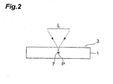
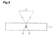
- Fig. 1 on a front face 3 of a wafer-like (planar) object to be processed 1, a line to cut 5 for cutting the object 1 exists.
- the line to cut 5 is a virtual line extending straight.
- the laser processing method in accordance with this embodiment irradiates the object 1 with laser light L while locating a converging point P within the object 1 under a condition generating multiphoton absorption, so as to form a modified region 7.
- the converging point P is a position at which the laser light L is converged.
- the line to cut 5 may be curved instead of being straight, and may be a line actually drawn on the object 1 without being restricted to the virtual line.
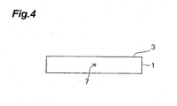
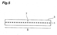
- the laser light L is relatively moved along the line to cut 5 (i.e., in the direction of arrow A in Fig. 1 ), so as to shift the converging point P along the line to cut 5. Consequently, as shown in Figs. 3 to 5 , the modified region 7 is formed along the line to cut 5 within the object 1 and becomes a starting point region for cutting 8.
- the starting point region for cutting 8 refers to a region which becomes a start point for cutting (fracturing) when the object 1 is cut.
- the starting point region for cutting 8 may be made by forming the modified region 7 either continuously or intermittently.
- the laser processing method in accordance with this embodiment is not one in which the object 1 absorbs the laser light L, thereby heating the object 1 and forming the modified region 7.
- the laser light L is transmitted through the object 1, so as to generate multiphoton absorption within the object 1, thereby forming the modified region 7. Therefore, the front face 3 of the object 1 hardly absorbs the laser light L and thus does not melt.
- Forming the starting point region for cutting 8 within the object 1 makes it easier to generate fractures from the starting point region for cutting 8 acting as a start point, whereby the object 1 can be cut with a relatively small force as shown in Fig. 6 . Therefore, the object 1 can be cut with a high precision without generating unnecessary fractures on the front face 3 of the object 1.
- the other is where the forming of the starting point region for cutting 8 causes the object 1 to fracture naturally in its cross-sectional direction (thickness direction) from the starting point region for cutting 8 acting as a start point, thereby cutting the object 1.
- the modified region formed by multiphoton absorption in the laser processing method in accordance with this embodiment encompasses the following cases (1) to (3):
- An object to be processed e.g., glass or a piezoelectric material made of LiTaO 3
- An object to be processed is irradiated with laser light while locating a converging point therewithin under a condition with a field intensity of at least 1 ⁇ 10 8 (W/cm 2 ) at the converging point and a pulse width of 1 ⁇ s or less.
- This magnitude of pulse width is a condition under which a crack region can be formed only within the object while generating multiphoton absorption without causing unnecessary damages on the front face of the object.
- This optical damage induces a thermal distortion within the object, thereby forming a crack region therewithin.
- the upper limit of field intensity is 1 ⁇ 10 12 (W/cm 2 ), for example.
- the pulse width is preferably 1 ns to 200 ns, for example.
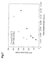
- the inventors determined the relationship between field intensity and crack size by an experiment. The following are conditions of the experiment.
- the laser light quality of TEM 00 means that the converging characteristic is so high that convergence to about the wavelength of laser light is possible.
- Fig. 7 is a graph showing the results of the above-mentioned experiment.
- the abscissa indicates the peak power density. Since the laser light is pulsed laser light, the field intensity is represented by the peak power density.
- the ordinate indicates the size of a crack part (crack spot) formed within the object by one pulse of laser light. Crack spots gather to yield a crack region. The crack spot size is the size of a part yielding the maximum length among forms of crack spots.
- Data represented by black circles in the graph refer to a case where the condenser lens (C) has a magnification of x100 and a numerical aperture (NA) of 0.80.
- data represented by whitened circles in the graph refer to a case where the condenser lens (C) has a magnification of x50 and a numerical aperture (NA) of 0.55. Crack spots are seen to occur within the object from when the peak power density is about 10 11 (W/cm 2 ) and become greater as the peak power density increases.
- FIG. 8 the object 1 is irradiated with laser light L while the converging point P is located within the object 1 under a condition where multiphoton absorption occurs, so as to form a crack region 9 therewithin along a line to cut.
- the crack region 9 is a region containing one crack or a plurality of cracks.
- formed crack region 9 becomes a starting point region for cutting.
- a crack further grows from the crack region 9 acting as a start point (i.e., from the starting point region for cutting acting as a start point) as shown in Fig.
- An object to be processed e.g., semiconductor material such as silicon
- An object to be processed is irradiated with laser light while locating a converging point within the object under a condition with a field intensity of at least 1 ⁇ 10 8 (W/cm 2 ) at the converging point and a pulse width of 1 ⁇ s or less.
- the inside of the object is locally heated by multiphoton absorption. This heating forms a molten processed region within the object.
- the molten processed region encompasses regions once molten and then re-solidified, regions just in a molten state, and regions in the process of being re-solidified from the molten state, and can also be referred to as a region whose phase has changed or a region whose crystal structure has changed.
- the molten processed region may also be referred to as a region in which a certain structure changes to another structure among monocrystal, amorphous, and polycrystal structures.
- the molten processed region is an amorphous silicon structure, for example.
- the upper limit of field intensity is 1 ⁇ 10 12 (W/cm 2 ), for example.
- the pulse width is preferably 1 ns to 200 ns, for example.
- the inventors verified that a molten processed region was formed within a silicon wafer (semiconductor substrate). The following are conditions of the experiment.
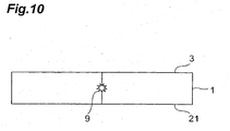
- Fig. 12 is a view showing a photograph of a cross section of a part of a silicon wafer cut by laser processing under the conditions mentioned above.
- a molten processed region 13 is formed within the silicon wafer 11.
- the molten processed region 13 formed under the above-mentioned conditions has a size of about 100 ⁇ m in the thickness direction.
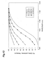
- Fig. 13 is a graph showing relationships between the laser light wavelength and the transmittance within the silicon substrate.
- the respective reflected components on the front and rear sides of the silicon substrate are eliminated, so as to show the internal transmittance alone.
- the respective relationships are shown in the cases where the thickness t of the silicon substrate is 50 ⁇ m, 100 ⁇ m, 200 ⁇ m, 500 ⁇ m, and 1000 ⁇ m.
- the laser light appears to be transmitted through the silicon substrate by at least 80% when the silicon substrate has a thickness of 500 ⁇ m or less.
- the silicon wafer 11 shown in Fig. 12 has a thickness of 350 ⁇ m, the molten processed region 13 caused by multiphoton absorption is formed near the center of the silicon wafer 11, i.e., at a part distanced from the front face by 175 ⁇ m.
- the transmittance in this case is 90% or more with reference to a silicon wafer having a thickness of 200 ⁇ m, whereby the laser light is absorbed only slightly within the silicon wafer 11 but is substantially transmitted therethrough.
- the molten processed region 13 is formed within the silicon wafer 11 not by laser light absorption within the silicon wafer 11 (i.e., not by usual heating with the laser light) but by multiphoton absorption.
- the forming of a molten processed region by multiphoton absorption is disclosed, for example, in " Silicon Processing Characteristic Evaluation by Picosecond Pulse Laser", Preprints of the National Meetings of Japan Welding Society, Vol. 66 (April, 2000), pp. 72-73 .
- a fracture is generated in a silicon wafer from a starting point region for cutting formed by a molten processed region, acting as a start point, in a cross-sectional direction, and reaches the front and rear faces of the silicon wafer, whereby the silicon wafer is cut.
- the fracture reaching the front and rear faces of the silicon wafer may grow naturally or as a force is applied to the silicon wafer.
- the fracture naturally growing from the starting point region for cutting to the front and rear faces of the silicon wafer encompasses a case where the fracture grows from a state where the molten processed region forming the starting point region for cutting is molten and a case where the fracture grows when the molten processed region forming the starting point region for cutting is re-solidified from the molten state.
- the molten processed region is formed only within the silicon wafer, and thus is present only within the cut section after cutting as shown in Fig. 12 .
- a starting point region for cutting is thus formed within the object by a molten processed region, unnecessary fractures deviating from a starting point region for cutting line are harder to occur at the time of cleaving, whereby cleavage control becomes easier.
- An object to be processed e.g., glass
- An object to be processed is irradiated with laser light while locating a converging point within the object under a condition with a field intensity of at least 1 ⁇ 10 8 (W/cm 2 ) at the converging point and a pulse width of 1 ns or less.
- a field intensity of at least 1 ⁇ 10 8 (W/cm 2 ) at the converging point and a pulse width of 1 ns or less.
- the upper limit of field intensity is 1 ⁇ 10 12 (W/cm 2 ), for example.
- the pulse width is preferably 1 ns or less, for example, more preferably 1 ps or less.
- the forming of a refractive index change region by multiphoton absorption is disclosed, for example, in " Forming of Photoinduced Structure within Glass by Femtosecond Laser Irradiation", Proceedings of the 42nd Laser Materials Processing Conference (November, 1997), pp. 105-111 .
- a starting point region for cutting may be formed as follows while taking account of the crystal structure of a wafer-like object to be processed, its cleavage characteristic, and the like, whereby the object can be cut with a favorable precision by a smaller force from the starting point region for cutting acting as a start point.
- a starting point region for cutting is formed in a direction extending along a (111) plane (first cleavage plane) or (110) plane (second cleavage plane).
- a substrate made of a group III-V compound semiconductor of sphalerite structure such as GaAs
- a starting point region for cutting is formed in a direction extending along a (1120) plane (A plane) or (1100) plane (M plane) while using a (0001) plane (C plane) as a principal plane.
- the starting point region for cutting extending in the direction to be formed with the starting point region for cutting can be formed easily and accurately in the substrate with reference to the orientation flat.
- Fig. 14 is a plan view of an object to be processed in the laser processing method in accordance with the embodiment, while Fig. 15 is a partial sectional view of the object taken along the line XV-XV of Fig. 14 .
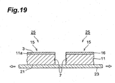
- an object to be processed 1 comprises a silicon wafer (semiconductor substrate) 11 having a thickness of 50 ⁇ m, and a functional device layer 16 which is formed on the front face 11 a of the silicon wafer 11 while including a plurality of functional devices 15.
- an expandable tape 23 is attached to the rear face 21 of the object 1.
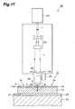
- the object 1 is fixed onto a mount table 51 of a laser processing apparatus 50 with the functional device layer 16 facing up.
- the silicon wafer 11 is irradiated with laser light L under a condition generating multiphoton absorption while locating the converging point P within the silicon wafer 11, and the mount table is moved, so as to scan the converging point P along each of lines to cut 5 (see broken lines of Fig. 14 ) set like a grid passing between the functional devices 15, 15 adjacent to each other.
- modified region 7 is a molten processed region, in which cracks may exist.
- the laser processing apparatus 50 comprises a laser head (laser light source) 52 for emitting the laser light L, a laser shaping optical system 53 for expanding the beam diameter of the emitted laser light L, and a pair of knife edges (changing means) 55 for forming a slit 54 which is positioned on the optical axis of the expanded laser light and extends in a direction parallel to the line to cut 5.
- a laser head laser light source
- a laser shaping optical system 53 for expanding the beam diameter of the emitted laser light L
- a pair of knife edges (changing means) 55 for forming a slit 54 which is positioned on the optical axis of the expanded laser light and extends in a direction parallel to the line to cut 5.
- the laser processing apparatus 50 further comprises an objective lens (condenser lens) 56 for converging the laser light L transmitted through the slit 54 and a piezoelectric device 57 for moving the objective lens 56 up and down in order to set the converging point to a position located at a constant depth from the front face 3 of the object 1.
- an objective lens condenser lens
- a piezoelectric device 57 for moving the objective lens 56 up and down in order to set the converging point to a position located at a constant depth from the front face 3 of the object 1.
- the beam diameter of the laser light L expanded by the laser shaping optical system 53 is 5 mm
- the width of the slit 54 is 1 mm
- the diameter of the entrance pupil of the objective lens 56 is 2.7 mm.
- the cross-sectional form (perpendicular to the optical axis) of the laser light L at the converging point P is such that the maximum length in the direction perpendicular to the line to cut 5 is shorter than the maximum length in the direction parallel to the line to cut 5 as shown in Fig. 18(a) .
- the intensity distribution of the laser light L at the converging point P is such that both skirt parts of a Gaussian distribution are cut off in the direction perpendicular to the line to cut 5 as shown in Fig. 18(b) .
- the knife edges 55 can advance and retract in horizontal directions with respect to the optical axis of the laser light L, so that changing the width of the slit 54 can alter the maximum length in the direction perpendicular to the line to cut 5.
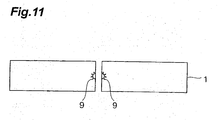
- the expandable tape 23 is expanded as shown in Fig. 19 , so that the fracture 24 also reaches the rear face 21 of the object 1 from the modified region 7 acting as a start point, thereby cutting the silicon wafer 11 and functional device layer 16 along the line to cut 5 and separating thus cut semiconductor chips 25 from each other.
- the cross-sectional form of the laser light L at the converging point P is such that the maximum length in the direction perpendicular to the line to cut 5 is shorter than the maximum length in the direction parallel to the line to cut 5. Therefore, when seen from the incident direction of the laser light, the shape of the modified region 7 formed within the silicon wafer 11 is such that the maximum length in the direction perpendicular to the line to cut 5 is shorter than the maximum length in the direction parallel to the line to cut 5. Forming the modified region 7 having such a shape within the object 1 can restrain twist hackles from occurring on cut surfaces when cutting the object 1 from the modified region 7 acting as a cutting start point, thereby making it possible to improve the flatness of the cut surfaces.
- twist hackles are restrained from occurring in the fracture 24 generated in the front face 3 of the object 1 from the modified region 7. This can hinder the fracture 24 from meandering and cranking and advance the fracture 24 substantially straight forward, which also contributes to improving the flatness of cut surfaces when cutting the object 1 from the modified region 7 acting as a cutting start point.
- the object 1 can reliably be cut into the semiconductor chips 25 (i.e., without leaving uncut parts) from the modified region 7 acting as a cutting start point if the fracture 24 extending along the line to cut 5 is generated in the front face 3 of the object 1 from the modified region 7.
- the laser light L has such a form that the maximum length in the direction perpendicular to the line to cut 5 is shorter than the maximum length in the direction parallel to the line to cut 5 on the front face 3 of the object 1 as well. Therefore, even when the functional devices 15 are susceptible to heat, the gap between the functional devices 15, 15 adjacent to each other can be narrowed, so that a greater number of semiconductor chips 25 can be obtained from the single object 1.
- the number of rows of modified regions 7 formed within the object 1 with respect to one line to cut 5 varies according to the thickness of the object 1 and the like, and thus is not limited to 1.
- the modified region 7 may also be formed such that the fracture 24 extending along the line to cut 5 is not generated in the front face 3 of the object 1 from the modified region 7.
- all the modified regions 7 are formed by irradiation with laser light L having such a cross-sectional form at the converging point P that the maximum length in the direction perpendicular to the line to cut 5 (hereinafter referred to as "perpendicular direction length") is shorter than the maximum length in the direction parallel to the line to cut 5 (hereinafter referred to as "parallel direction length").
- perpendicular direction length the maximum length in the direction perpendicular to the line to cut 5
- parallel direction length the maximum length in the direction parallel to the line to cut 5
- the modified region 7 formed at a position deeper from the laser light incident surface of the object 1 may fail to have an appropriate dividing effect, since the energy of laser light L becomes lower than that in the modified region 7 formed at a shallower position under the influence of the converging ratio of laser light L within the object 1.
- the laser light L having such a cross-sectional form that the perpendicular direction length is shorter than the parallel direction length is emitted when forming the modified region 7 at a position shallower from the laser light incident surface of the object 1, and laser light L having such a cross-sectional form that the perpendicular direction length is longer than that at the time of forming the modified region 7 at the shallower position is emitted when forming the modified region 7 at a deeper position.
- a plurality of rows of modified regions 7 may be formed with respect to one line to cut 5 such that at least one of the first and second rows of modified regions 7 from the laser light incident surface of the object 1 is formed by irradiation with laser light having such a cross-sectional form that the perpendicular direction length is shorter than the parallel direction length (hereinafter referred to as "shaped laser light”), and the remaining modified regions 7 are formed by irradiation with laser light having such a cross-sectional form that the perpendicular direction length and the parallel direction length are substantially equal to each other (hereinafter referred to as "unshaped laser light").
- the shaped laser light and unshaped laser light can be switched therebetween in the following manner in the above-mentioned laser processing apparatus 50. Namely, the knife edges 55 are advanced with respect to the optical axis of the laser light L, so as to narrow the width of the slit 54, thereby yielding the shaped laser light. On the other hand, the knife edges 55 are retracted with respect to the optical axis of the laser light L, so as to widen the width of the slit 54, thereby yielding the unshaped laser light.
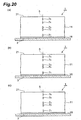
- Fig. 20 is a partial sectional view of an object to be processed 1 formed with five rows of modified regions 7 1 to 7 5 with respect to one line to cut 5, in which (a) is a case where the first and second rows of modified regions 7 4 , 7 5 from the rear face 21 of the object 1 are formed by irradiation with the shaped laser light, while the remaining modified regions 7 1 to 7 3 are formed by irradiation with the unshaped laser light; (b) is a case where the second row of modified regions 7 4 from the rear face 21 of the object 1 is formed by irradiation with the shaped laser light, while the remaining modified regions 7 1 to 7 3 , 7 5 are formed by irradiation with the unshaped laser light; and (c) is a case where the first row of modified regions 7 5 from the rear face 21 of the object 1 is formed by irradiation with the shaped laser light, while the remaining modified regions 7 1 to 7 4 are formed by irradiation with the unshaped laser light.
- Fig. 20(a) is effective in generating a deep fracture along the line to cut 5 in the rear face 21
- Fig. 20(b) is effective in generating a shallow fracture along the line to cut 5 in the rear face 21, they are not always aimed at generating fractures.
- the above-mentioned embodiments relate to a case where the front face 3 of the object 1 is the laser light incident surface, the rear face 21 of the object 1 may be employed as the laser light incident surface.
- the above-mentioned embodiments relate to a case where the functional device layer 16 is present on the line to cut 5, the front face 11a of the silicon wafer 11 may be employed as the laser light incident surface in a state where no functional device layer 16 is present on the line to cut 5 while exposing the front face 11a of the silicon wafer 11.
- the present invention can improve the flatness of cut surfaces when cutting an object to be processed from a modified region acting as a starting point region for cutting.
Claims (6)
- Procédé de traitement au laser pour former une pluralité de rangées de régions modifiées (7) destinées à devenir un point de départ de coupe au sein d'un objet (1) destiné à être traité le long d'une ligne de coupe (5) de l'objet (1) en irradiant l'objet (1) avec une lumière laser (L) tout en localisant un point de convergence (P) au sein de l'objet (1) ;
dans lequel une région modifiée prédéterminée (7) est formée par irradiation avec une lumière laser prédéterminée (L) dont la forme en coupe au point de convergence (P) est telle que la longueur maximale dans une direction perpendiculaire à la ligne de coupe (5) est plus courte que la longueur maximale dans une direction parallèle à la ligne de coupe (5) ;
dans lequel, lors de la formation de ladite pluralité de rangées de régions modifiées (7) par rapport à une ligne de coupe (5), la lumière laser prédéterminée (L) ayant une forme en coupe au point de convergence (P) telle que la longueur maximale dans la direction perpendiculaire à la ligne de coupe (5) est plus courte que la longueur maximale dans la direction parallèle à la ligne de coupe (5) est émise lors de la formation de la région modifiée (7) dans une position plus superficielle par rapport à la surface d'incidence de la lumière laser (L) de l'objet (1), caractérisé en ce que la lumière laser prédéterminée (L) ayant une forme en coupe au point de convergence (P) telle que la longueur maximale dans la direction perpendiculaire à la ligne de coupe (5) est plus longue qu'au moment de la formation de la région modifiée (7) dans la position plus superficielle est émise lors de la formation de la région modifiée (7) dans une position plus profonde par rapport à la surface d'incidence de la lumière laser (L). - Procédé de traitement au laser selon la revendication 1, dans lequel, lors de la formation d'une pluralité de rangées de la région modifiée (7) par rapport à une ligne de coupe (5), au moins une des première et seconde rangées de la région modifiée (7) par rapport à la surface d'incidence de la lumière laser (L) de l'objet (1) constitue la région modifiée prédéterminée (7) ;
dans lequel, lors de la formation d'une pluralité de rangées de régions modifiées (7) par rapport à une ligne de coupe (5), au moins une des première et seconde rangées de régions modifiées (7) par rapport à la surface d'incidence de la lumière laser (L) de l'objet (1) est formée par irradiation avec la lumière laser prédéterminée (L), et les régions modifiées restantes (7) sont formées par irradiation avec la lumière laser (L) ayant une forme en coupe au point de convergence (P) telle que la longueur maximale dans la direction perpendiculaire à la ligne de coupe (5) et la longueur maximale dans la direction parallèle à la ligne de coupe (5) sont sensiblement égales entre elles. - Procédé de traitement au laser selon la revendication 1, dans lequel une fracture (24) s'étendant le long de la ligne de coupe (5) est générée dans la surface d'incidence de la lumière laser (L) de l'objet (1) par rapport à la région modifiée prédéterminée (7) par formation de la région modifiée prédéterminée (7).
- Procédé de traitement au laser selon la revendication 1, dans lequel, après formation de la région modifiée (7) au sein de l'objet (1), l'objet (1) est découpé le long de la ligne de coupe (5) par rapport à la région modifiée (7) jouant le rôle de région de point de départ de coupe.
- Procédé de traitement au laser selon la revendication 1, dans lequel l'objet (1) et muni d'un substrat semiconducteur (11) et dans lequel la région modifiée (7) comporte une région traitée fondue (13).
- Procédé de traitement au laser selon la revendication 1, dans lequel la distribution d'intensité de la lumière laser prédéterminée (L) au point de convergence (P) est telle que les deux parties de jupe d'une distribution gaussienne sont coupées dans la direction perpendiculaire à la ligne de coupe (5).
Applications Claiming Priority (2)
| Application Number | Priority Date | Filing Date | Title |
|---|---|---|---|
| JP2005270817A JP4762653B2 (ja) | 2005-09-16 | 2005-09-16 | レーザ加工方法及びレーザ加工装置 |
| PCT/JP2006/318163 WO2007032392A1 (fr) | 2005-09-16 | 2006-09-13 | Procédé et dispositif de traitement laser |
Publications (3)
| Publication Number | Publication Date |
|---|---|
| EP1944118A1 EP1944118A1 (fr) | 2008-07-16 |
| EP1944118A4 EP1944118A4 (fr) | 2009-09-16 |
| EP1944118B1 true EP1944118B1 (fr) | 2015-11-04 |
Family
ID=37864983
Family Applications (1)
| Application Number | Title | Priority Date | Filing Date |
|---|---|---|---|
| EP06797913.8A Active EP1944118B1 (fr) | 2005-09-16 | 2006-09-13 | Procédé de traitement laser |
Country Status (7)
| Country | Link |
|---|---|
| US (1) | US8513567B2 (fr) |
| EP (1) | EP1944118B1 (fr) |
| JP (1) | JP4762653B2 (fr) |
| KR (1) | KR101349556B1 (fr) |
| CN (2) | CN101227999B (fr) |
| TW (1) | TWI463550B (fr) |
| WO (1) | WO2007032392A1 (fr) |
Families Citing this family (56)
| Publication number | Priority date | Publication date | Assignee | Title |
|---|---|---|---|---|
| JP4659300B2 (ja) | 2000-09-13 | 2011-03-30 | 浜松ホトニクス株式会社 | レーザ加工方法及び半導体チップの製造方法 |
| EP2216128B1 (fr) * | 2002-03-12 | 2016-01-27 | Hamamatsu Photonics K.K. | Procédé de coupage d'un object usiné |
| TWI326626B (en) | 2002-03-12 | 2010-07-01 | Hamamatsu Photonics Kk | Laser processing method |
| EP2400539B1 (fr) | 2002-03-12 | 2017-07-26 | Hamamatsu Photonics K.K. | Methode pour la division d'un substrat |
| TWI520269B (zh) | 2002-12-03 | 2016-02-01 | Hamamatsu Photonics Kk | Cutting method of semiconductor substrate |
| FR2852250B1 (fr) | 2003-03-11 | 2009-07-24 | Jean Luc Jouvin | Fourreau de protection pour canule, un ensemble d'injection comportant un tel fourreau et aiguille equipee d'un tel fourreau |
| US8685838B2 (en) | 2003-03-12 | 2014-04-01 | Hamamatsu Photonics K.K. | Laser beam machining method |
| EP2269765B1 (fr) * | 2003-07-18 | 2014-10-15 | Hamamatsu Photonics K.K. | Chip semiconducteur découpé |
| JP4563097B2 (ja) | 2003-09-10 | 2010-10-13 | 浜松ホトニクス株式会社 | 半導体基板の切断方法 |
| JP4601965B2 (ja) * | 2004-01-09 | 2010-12-22 | 浜松ホトニクス株式会社 | レーザ加工方法及びレーザ加工装置 |
| JP4509578B2 (ja) | 2004-01-09 | 2010-07-21 | 浜松ホトニクス株式会社 | レーザ加工方法及びレーザ加工装置 |
| JP4598407B2 (ja) * | 2004-01-09 | 2010-12-15 | 浜松ホトニクス株式会社 | レーザ加工方法及びレーザ加工装置 |
| KR101336523B1 (ko) | 2004-03-30 | 2013-12-03 | 하마마츠 포토닉스 가부시키가이샤 | 레이저 가공 방법 및 반도체 칩 |
| JP4200177B2 (ja) * | 2004-08-06 | 2008-12-24 | 浜松ホトニクス株式会社 | レーザ加工方法及び半導体装置 |
| US9138913B2 (en) * | 2005-09-08 | 2015-09-22 | Imra America, Inc. | Transparent material processing with an ultrashort pulse laser |
| DE102006042280A1 (de) | 2005-09-08 | 2007-06-06 | IMRA America, Inc., Ann Arbor | Bearbeitung von transparentem Material mit einem Ultrakurzpuls-Laser |
| JP4907965B2 (ja) * | 2005-11-25 | 2012-04-04 | 浜松ホトニクス株式会社 | レーザ加工方法 |
| JP4804911B2 (ja) * | 2005-12-22 | 2011-11-02 | 浜松ホトニクス株式会社 | レーザ加工装置 |
| JP4907984B2 (ja) * | 2005-12-27 | 2012-04-04 | 浜松ホトニクス株式会社 | レーザ加工方法及び半導体チップ |
| US7897487B2 (en) | 2006-07-03 | 2011-03-01 | Hamamatsu Photonics K.K. | Laser processing method and chip |
| JP5183892B2 (ja) | 2006-07-03 | 2013-04-17 | 浜松ホトニクス株式会社 | レーザ加工方法 |
| JP4954653B2 (ja) | 2006-09-19 | 2012-06-20 | 浜松ホトニクス株式会社 | レーザ加工方法 |
| US8188404B2 (en) * | 2006-09-19 | 2012-05-29 | Hamamatsu Photonics K.K. | Laser processing method and laser processing apparatus |
| JP5101073B2 (ja) * | 2006-10-02 | 2012-12-19 | 浜松ホトニクス株式会社 | レーザ加工装置 |
| JP4964554B2 (ja) * | 2006-10-03 | 2012-07-04 | 浜松ホトニクス株式会社 | レーザ加工方法 |
| JP5132911B2 (ja) * | 2006-10-03 | 2013-01-30 | 浜松ホトニクス株式会社 | レーザ加工方法 |
| EP2070636B1 (fr) * | 2006-10-04 | 2015-08-05 | Hamamatsu Photonics K.K. | Procédé de traitement laser |
| JP5336054B2 (ja) | 2007-07-18 | 2013-11-06 | 浜松ホトニクス株式会社 | 加工情報供給装置を備える加工情報供給システム |
| JP5188764B2 (ja) * | 2007-08-29 | 2013-04-24 | 浜松ホトニクス株式会社 | レーザ加工装置およびレーザ加工方法 |
| JP5449665B2 (ja) | 2007-10-30 | 2014-03-19 | 浜松ホトニクス株式会社 | レーザ加工方法 |
| JP5134928B2 (ja) * | 2007-11-30 | 2013-01-30 | 浜松ホトニクス株式会社 | 加工対象物研削方法 |
| JP5054496B2 (ja) * | 2007-11-30 | 2012-10-24 | 浜松ホトニクス株式会社 | 加工対象物切断方法 |
| JP2009220142A (ja) * | 2008-03-17 | 2009-10-01 | Sony Corp | レーザー加工装置及びレーザー加工方法 |
| JP5692969B2 (ja) | 2008-09-01 | 2015-04-01 | 浜松ホトニクス株式会社 | 収差補正方法、この収差補正方法を用いたレーザ加工方法、この収差補正方法を用いたレーザ照射方法、収差補正装置、及び、収差補正プログラム |
| JP5254761B2 (ja) | 2008-11-28 | 2013-08-07 | 浜松ホトニクス株式会社 | レーザ加工装置 |
| JP5241525B2 (ja) | 2009-01-09 | 2013-07-17 | 浜松ホトニクス株式会社 | レーザ加工装置 |
| JP5241527B2 (ja) | 2009-01-09 | 2013-07-17 | 浜松ホトニクス株式会社 | レーザ加工装置 |
| JP5632751B2 (ja) | 2009-02-09 | 2014-11-26 | 浜松ホトニクス株式会社 | 加工対象物切断方法 |
| CN102317030B (zh) | 2009-04-07 | 2014-08-20 | 浜松光子学株式会社 | 激光加工装置以及激光加工方法 |
| JP5491761B2 (ja) | 2009-04-20 | 2014-05-14 | 浜松ホトニクス株式会社 | レーザ加工装置 |
| JP5476063B2 (ja) | 2009-07-28 | 2014-04-23 | 浜松ホトニクス株式会社 | 加工対象物切断方法 |
| DE102010009015A1 (de) * | 2010-02-24 | 2011-08-25 | OSRAM Opto Semiconductors GmbH, 93055 | Verfahren zum Herstellen einer Mehrzahl von optoelektronischen Halbleiterchips |
| KR100984726B1 (ko) * | 2010-04-28 | 2010-10-01 | 유병소 | 레이저를 이용한 대상물 가공 방법, 대상물 가공 장치, 및 대상물 가공 시스템 |
| KR100984727B1 (ko) | 2010-04-30 | 2010-10-01 | 유병소 | 대상물 가공 방법 및 대상물 가공 장치 |
| JP5552373B2 (ja) | 2010-06-02 | 2014-07-16 | 浜松ホトニクス株式会社 | レーザ加工方法 |
| KR101211104B1 (ko) * | 2010-08-18 | 2012-12-18 | 유병소 | 레이저 가공 방법 및 레이저 가공 장치 |
| US8722516B2 (en) | 2010-09-28 | 2014-05-13 | Hamamatsu Photonics K.K. | Laser processing method and method for manufacturing light-emitting device |
| JP2013031880A (ja) * | 2012-09-12 | 2013-02-14 | Hamamatsu Photonics Kk | レーザ加工装置およびレーザ加工方法 |
| JP6325279B2 (ja) * | 2014-02-21 | 2018-05-16 | 株式会社ディスコ | ウエーハの加工方法 |
| JP2016058429A (ja) * | 2014-09-05 | 2016-04-21 | 株式会社ディスコ | ウエーハの加工方法 |
| US10518358B1 (en) | 2016-01-28 | 2019-12-31 | AdlOptica Optical Systems GmbH | Multi-focus optics |
| US10589445B1 (en) * | 2018-10-29 | 2020-03-17 | Semivation, LLC | Method of cleaving a single crystal substrate parallel to its active planar surface and method of using the cleaved daughter substrate |
| US10576585B1 (en) | 2018-12-29 | 2020-03-03 | Cree, Inc. | Laser-assisted method for parting crystalline material |
| US11024501B2 (en) | 2018-12-29 | 2021-06-01 | Cree, Inc. | Carrier-assisted method for parting crystalline material along laser damage region |
| US10562130B1 (en) | 2018-12-29 | 2020-02-18 | Cree, Inc. | Laser-assisted method for parting crystalline material |
| US10611052B1 (en) | 2019-05-17 | 2020-04-07 | Cree, Inc. | Silicon carbide wafers with relaxed positive bow and related methods |
Family Cites Families (65)
| Publication number | Priority date | Publication date | Assignee | Title |
|---|---|---|---|---|
| JP2691029B2 (ja) * | 1989-10-18 | 1997-12-17 | 株式会社日立製作所 | レーザー装置 |
| DE69115353T2 (de) * | 1990-05-30 | 1996-05-09 | Hitachi Ltd | Laserbearbeitungsgerät und dessen Verfahren |
| JP3044811B2 (ja) * | 1991-03-25 | 2000-05-22 | 日本電気株式会社 | フォトマスク修正装置 |
| DE4305107C2 (de) * | 1993-02-19 | 1995-02-23 | Fraunhofer Ges Forschung | Verfahren und Vorrichtung zum Schneiden eines spröden Körpers mit Laserstrahlung |
| JPH081363A (ja) | 1994-06-17 | 1996-01-09 | Sony Corp | Ic解析用のパターンカッティング装置 |
| US5776220A (en) * | 1994-09-19 | 1998-07-07 | Corning Incorporated | Method and apparatus for breaking brittle materials |
| JPH09150286A (ja) | 1995-06-26 | 1997-06-10 | Corning Inc | 脆弱性材料切断方法および装置 |
| JPH10258385A (ja) * | 1997-03-14 | 1998-09-29 | Komatsu Ltd | レーザ加工機、レーザ加工機の加工方法、及びレーザ加工機用マスク |
| US6211488B1 (en) | 1998-12-01 | 2001-04-03 | Accudyne Display And Semiconductor Systems, Inc. | Method and apparatus for separating non-metallic substrates utilizing a laser initiated scribe |
| JP2000263257A (ja) | 1999-03-15 | 2000-09-26 | Hitachi Cable Ltd | 非金属材料のレーザによる割断方法及びその装置 |
| US8217304B2 (en) * | 2001-03-29 | 2012-07-10 | Gsi Group Corporation | Methods and systems for thermal-based laser processing a multi-material device |
| JP4659300B2 (ja) | 2000-09-13 | 2011-03-30 | 浜松ホトニクス株式会社 | レーザ加工方法及び半導体チップの製造方法 |
| JP4286488B2 (ja) * | 2001-02-21 | 2009-07-01 | キヤノンマシナリー株式会社 | 基板切断方法 |
| EP2216128B1 (fr) | 2002-03-12 | 2016-01-27 | Hamamatsu Photonics K.K. | Procédé de coupage d'un object usiné |
| EP2400539B1 (fr) | 2002-03-12 | 2017-07-26 | Hamamatsu Photonics K.K. | Methode pour la division d'un substrat |
| TWI326626B (en) | 2002-03-12 | 2010-07-01 | Hamamatsu Photonics Kk | Laser processing method |
| JP4050534B2 (ja) | 2002-03-12 | 2008-02-20 | 浜松ホトニクス株式会社 | レーザ加工方法 |
| JP2004179302A (ja) | 2002-11-26 | 2004-06-24 | Disco Abrasive Syst Ltd | 半導体ウエーハの分割方法 |
| TWI520269B (zh) | 2002-12-03 | 2016-02-01 | Hamamatsu Photonics Kk | Cutting method of semiconductor substrate |
| CN100445014C (zh) | 2002-12-05 | 2008-12-24 | 浜松光子学株式会社 | 激光加工装置 |
| JP2004188422A (ja) | 2002-12-06 | 2004-07-08 | Hamamatsu Photonics Kk | レーザ加工装置及びレーザ加工方法 |
| FR2852250B1 (fr) | 2003-03-11 | 2009-07-24 | Jean Luc Jouvin | Fourreau de protection pour canule, un ensemble d'injection comportant un tel fourreau et aiguille equipee d'un tel fourreau |
| US8685838B2 (en) | 2003-03-12 | 2014-04-01 | Hamamatsu Photonics K.K. | Laser beam machining method |
| EP2269765B1 (fr) | 2003-07-18 | 2014-10-15 | Hamamatsu Photonics K.K. | Chip semiconducteur découpé |
| JP4563097B2 (ja) | 2003-09-10 | 2010-10-13 | 浜松ホトニクス株式会社 | 半導体基板の切断方法 |
| JP2005086175A (ja) | 2003-09-11 | 2005-03-31 | Hamamatsu Photonics Kk | 半導体薄膜の製造方法、半導体薄膜、半導体薄膜チップ、電子管、及び光検出素子 |
| JP2005116844A (ja) * | 2003-10-09 | 2005-04-28 | Matsushita Electric Ind Co Ltd | 半導体装置の製造方法 |
| JP4397229B2 (ja) * | 2003-12-25 | 2010-01-13 | 株式会社ブイ・テクノロジー | レーザ加工装置 |
| KR101195311B1 (ko) | 2004-01-07 | 2012-10-26 | 하마마츠 포토닉스 가부시키가이샤 | 반도체 발광 소자 및 그 제조 방법 |
| JP4601965B2 (ja) | 2004-01-09 | 2010-12-22 | 浜松ホトニクス株式会社 | レーザ加工方法及びレーザ加工装置 |
| JP4598407B2 (ja) | 2004-01-09 | 2010-12-15 | 浜松ホトニクス株式会社 | レーザ加工方法及びレーザ加工装置 |
| JP4509578B2 (ja) | 2004-01-09 | 2010-07-21 | 浜松ホトニクス株式会社 | レーザ加工方法及びレーザ加工装置 |
| JP4086796B2 (ja) * | 2004-02-19 | 2008-05-14 | キヤノン株式会社 | 基板割断方法 |
| JP4536407B2 (ja) | 2004-03-30 | 2010-09-01 | 浜松ホトニクス株式会社 | レーザ加工方法及び加工対象物 |
| KR101336523B1 (ko) | 2004-03-30 | 2013-12-03 | 하마마츠 포토닉스 가부시키가이샤 | 레이저 가공 방법 및 반도체 칩 |
| EP1748474B1 (fr) | 2004-03-30 | 2015-05-06 | Hamamatsu Photonics K.K. | Procede de traitement au laser |
| US20080135532A1 (en) | 2004-04-27 | 2008-06-12 | Mitsuboshi Diamond Industrial Co., Ltd. | Method of and an Apparatus for Forming a Perpendicular Crack in a Brittle Substrate |
| JP4634089B2 (ja) | 2004-07-30 | 2011-02-16 | 浜松ホトニクス株式会社 | レーザ加工方法 |
| JP4200177B2 (ja) | 2004-08-06 | 2008-12-24 | 浜松ホトニクス株式会社 | レーザ加工方法及び半導体装置 |
| JP4754801B2 (ja) | 2004-10-13 | 2011-08-24 | 浜松ホトニクス株式会社 | レーザ加工方法 |
| JP4781661B2 (ja) | 2004-11-12 | 2011-09-28 | 浜松ホトニクス株式会社 | レーザ加工方法 |
| JP4917257B2 (ja) | 2004-11-12 | 2012-04-18 | 浜松ホトニクス株式会社 | レーザ加工方法 |
| JP4198123B2 (ja) | 2005-03-22 | 2008-12-17 | 浜松ホトニクス株式会社 | レーザ加工方法 |
| JP4776994B2 (ja) | 2005-07-04 | 2011-09-21 | 浜松ホトニクス株式会社 | 加工対象物切断方法 |
| JP4749799B2 (ja) | 2005-08-12 | 2011-08-17 | 浜松ホトニクス株式会社 | レーザ加工方法 |
| JP4237745B2 (ja) | 2005-11-18 | 2009-03-11 | 浜松ホトニクス株式会社 | レーザ加工方法 |
| JP4907965B2 (ja) | 2005-11-25 | 2012-04-04 | 浜松ホトニクス株式会社 | レーザ加工方法 |
| JP4804911B2 (ja) | 2005-12-22 | 2011-11-02 | 浜松ホトニクス株式会社 | レーザ加工装置 |
| JP4907984B2 (ja) | 2005-12-27 | 2012-04-04 | 浜松ホトニクス株式会社 | レーザ加工方法及び半導体チップ |
| US7897487B2 (en) | 2006-07-03 | 2011-03-01 | Hamamatsu Photonics K.K. | Laser processing method and chip |
| JP5183892B2 (ja) | 2006-07-03 | 2013-04-17 | 浜松ホトニクス株式会社 | レーザ加工方法 |
| US8188404B2 (en) | 2006-09-19 | 2012-05-29 | Hamamatsu Photonics K.K. | Laser processing method and laser processing apparatus |
| JP4954653B2 (ja) | 2006-09-19 | 2012-06-20 | 浜松ホトニクス株式会社 | レーザ加工方法 |
| JP5101073B2 (ja) | 2006-10-02 | 2012-12-19 | 浜松ホトニクス株式会社 | レーザ加工装置 |
| JP4964554B2 (ja) | 2006-10-03 | 2012-07-04 | 浜松ホトニクス株式会社 | レーザ加工方法 |
| JP5132911B2 (ja) | 2006-10-03 | 2013-01-30 | 浜松ホトニクス株式会社 | レーザ加工方法 |
| EP2070636B1 (fr) | 2006-10-04 | 2015-08-05 | Hamamatsu Photonics K.K. | Procédé de traitement laser |
| JP5336054B2 (ja) | 2007-07-18 | 2013-11-06 | 浜松ホトニクス株式会社 | 加工情報供給装置を備える加工情報供給システム |
| JP4402708B2 (ja) | 2007-08-03 | 2010-01-20 | 浜松ホトニクス株式会社 | レーザ加工方法、レーザ加工装置及びその製造方法 |
| JP5225639B2 (ja) | 2007-09-06 | 2013-07-03 | 浜松ホトニクス株式会社 | 半導体レーザ素子の製造方法 |
| JP5342772B2 (ja) | 2007-10-12 | 2013-11-13 | 浜松ホトニクス株式会社 | 加工対象物切断方法 |
| JP5449665B2 (ja) | 2007-10-30 | 2014-03-19 | 浜松ホトニクス株式会社 | レーザ加工方法 |
| JP5134928B2 (ja) | 2007-11-30 | 2013-01-30 | 浜松ホトニクス株式会社 | 加工対象物研削方法 |
| JP5054496B2 (ja) | 2007-11-30 | 2012-10-24 | 浜松ホトニクス株式会社 | 加工対象物切断方法 |
| JP5241525B2 (ja) | 2009-01-09 | 2013-07-17 | 浜松ホトニクス株式会社 | レーザ加工装置 |
-
2005
- 2005-09-16 JP JP2005270817A patent/JP4762653B2/ja active Active
-
2006
- 2006-09-13 KR KR1020077025750A patent/KR101349556B1/ko active IP Right Grant
- 2006-09-13 CN CN2006800268644A patent/CN101227999B/zh active Active
- 2006-09-13 US US12/064,275 patent/US8513567B2/en active Active
- 2006-09-13 CN CN2011100270350A patent/CN102172799B/zh active Active
- 2006-09-13 EP EP06797913.8A patent/EP1944118B1/fr active Active
- 2006-09-13 WO PCT/JP2006/318163 patent/WO2007032392A1/fr active Application Filing
- 2006-09-15 TW TW095134354A patent/TWI463550B/zh active
Also Published As
| Publication number | Publication date |
|---|---|
| CN102172799A (zh) | 2011-09-07 |
| US20090261083A1 (en) | 2009-10-22 |
| KR101349556B1 (ko) | 2014-01-10 |
| JP2007075886A (ja) | 2007-03-29 |
| CN101227999A (zh) | 2008-07-23 |
| CN101227999B (zh) | 2011-03-30 |
| TWI463550B (zh) | 2014-12-01 |
| EP1944118A4 (fr) | 2009-09-16 |
| JP4762653B2 (ja) | 2011-08-31 |
| CN102172799B (zh) | 2013-11-06 |
| US8513567B2 (en) | 2013-08-20 |
| EP1944118A1 (fr) | 2008-07-16 |
| WO2007032392A1 (fr) | 2007-03-22 |
| KR20080050547A (ko) | 2008-06-09 |
| TW200721286A (en) | 2007-06-01 |
Similar Documents
| Publication | Publication Date | Title |
|---|---|---|
| EP1944118B1 (fr) | Procédé de traitement laser | |
| EP1983557B1 (fr) | Procede d' usinage par faisceau laser | |
| EP1875983B1 (fr) | Procédé de traitement laser et puce obtenue | |
| EP1867427B1 (fr) | Procede d usinage au laser | |
| EP1959482B1 (fr) | Procédé de traitement au laser | |
| EP2070636B1 (fr) | Procédé de traitement laser | |
| EP2070632B1 (fr) | Procédé de traitement au laser | |
| EP1742252B1 (fr) | Procede de traitement laser | |
| US8026154B2 (en) | Laser working method | |
| EP1906438B1 (fr) | Procédé de découpe de pièce | |
| EP2065120B1 (fr) | Procédé de traitement au laser | |
| EP1956640B1 (fr) | Procede de traitement laser | |
| EP1920874A1 (fr) | Procédé de traitement au laser |
Legal Events
| Date | Code | Title | Description |
|---|---|---|---|
| PUAI | Public reference made under article 153(3) epc to a published international application that has entered the european phase |
Free format text: ORIGINAL CODE: 0009012 |
|
| 17P | Request for examination filed |
Effective date: 20080318 |
|
| AK | Designated contracting states |
Kind code of ref document: A1 Designated state(s): AT BE BG CH CY CZ DE DK EE ES FI FR GB GR HU IE IS IT LI LT LU LV MC NL PL PT RO SE SI SK TR |
|
| A4 | Supplementary search report drawn up and despatched |
Effective date: 20090813 |
|
| RIC1 | Information provided on ipc code assigned before grant |
Ipc: H01L 21/78 20060101ALI20090807BHEP Ipc: B23K 26/00 20060101ALI20090807BHEP Ipc: B23K 26/06 20060101ALI20090807BHEP Ipc: B23K 26/40 20060101AFI20070524BHEP Ipc: B23K 26/073 20060101ALI20090807BHEP Ipc: B28D 5/00 20060101ALI20090807BHEP Ipc: B23K 101/40 20060101ALN20090807BHEP |
|
| 17Q | First examination report despatched |
Effective date: 20091223 |
|
| DAX | Request for extension of the european patent (deleted) | ||
| GRAP | Despatch of communication of intention to grant a patent |
Free format text: ORIGINAL CODE: EPIDOSNIGR1 |
|
| INTG | Intention to grant announced |
Effective date: 20150409 |
|
| GRAS | Grant fee paid |
Free format text: ORIGINAL CODE: EPIDOSNIGR3 |
|
| GRAA | (expected) grant |
Free format text: ORIGINAL CODE: 0009210 |
|
| AK | Designated contracting states |
Kind code of ref document: B1 Designated state(s): AT BE BG CH CY CZ DE DK EE ES FI FR GB GR HU IE IS IT LI LT LU LV MC NL PL PT RO SE SI SK TR |
|
| REG | Reference to a national code |
Ref country code: GB Ref legal event code: FG4D |
|
| REG | Reference to a national code |
Ref country code: CH Ref legal event code: EP |
|
| REG | Reference to a national code |
Ref country code: AT Ref legal event code: REF Ref document number: 758857 Country of ref document: AT Kind code of ref document: T Effective date: 20151115 |
|
| REG | Reference to a national code |
Ref country code: IE Ref legal event code: FG4D |
|
| REG | Reference to a national code |
Ref country code: DE Ref legal event code: R096 Ref document number: 602006047179 Country of ref document: DE |
|
| REG | Reference to a national code |
Ref country code: NL Ref legal event code: MP Effective date: 20151104 |
|
| REG | Reference to a national code |
Ref country code: LT Ref legal event code: MG4D |
|
| REG | Reference to a national code |
Ref country code: AT Ref legal event code: MK05 Ref document number: 758857 Country of ref document: AT Kind code of ref document: T Effective date: 20151104 |
|
| PG25 | Lapsed in a contracting state [announced via postgrant information from national office to epo] |
Ref country code: LT Free format text: LAPSE BECAUSE OF FAILURE TO SUBMIT A TRANSLATION OF THE DESCRIPTION OR TO PAY THE FEE WITHIN THE PRESCRIBED TIME-LIMIT Effective date: 20151104 Ref country code: IT Free format text: LAPSE BECAUSE OF FAILURE TO SUBMIT A TRANSLATION OF THE DESCRIPTION OR TO PAY THE FEE WITHIN THE PRESCRIBED TIME-LIMIT Effective date: 20151104 Ref country code: NL Free format text: LAPSE BECAUSE OF FAILURE TO SUBMIT A TRANSLATION OF THE DESCRIPTION OR TO PAY THE FEE WITHIN THE PRESCRIBED TIME-LIMIT Effective date: 20151104 Ref country code: IS Free format text: LAPSE BECAUSE OF FAILURE TO SUBMIT A TRANSLATION OF THE DESCRIPTION OR TO PAY THE FEE WITHIN THE PRESCRIBED TIME-LIMIT Effective date: 20160304 Ref country code: ES Free format text: LAPSE BECAUSE OF FAILURE TO SUBMIT A TRANSLATION OF THE DESCRIPTION OR TO PAY THE FEE WITHIN THE PRESCRIBED TIME-LIMIT Effective date: 20151104 |
|
| PG25 | Lapsed in a contracting state [announced via postgrant information from national office to epo] |
Ref country code: LV Free format text: LAPSE BECAUSE OF FAILURE TO SUBMIT A TRANSLATION OF THE DESCRIPTION OR TO PAY THE FEE WITHIN THE PRESCRIBED TIME-LIMIT Effective date: 20151104 Ref country code: PL Free format text: LAPSE BECAUSE OF FAILURE TO SUBMIT A TRANSLATION OF THE DESCRIPTION OR TO PAY THE FEE WITHIN THE PRESCRIBED TIME-LIMIT Effective date: 20151104 Ref country code: PT Free format text: LAPSE BECAUSE OF FAILURE TO SUBMIT A TRANSLATION OF THE DESCRIPTION OR TO PAY THE FEE WITHIN THE PRESCRIBED TIME-LIMIT Effective date: 20160304 Ref country code: AT Free format text: LAPSE BECAUSE OF FAILURE TO SUBMIT A TRANSLATION OF THE DESCRIPTION OR TO PAY THE FEE WITHIN THE PRESCRIBED TIME-LIMIT Effective date: 20151104 Ref country code: SE Free format text: LAPSE BECAUSE OF FAILURE TO SUBMIT A TRANSLATION OF THE DESCRIPTION OR TO PAY THE FEE WITHIN THE PRESCRIBED TIME-LIMIT Effective date: 20151104 Ref country code: GR Free format text: LAPSE BECAUSE OF FAILURE TO SUBMIT A TRANSLATION OF THE DESCRIPTION OR TO PAY THE FEE WITHIN THE PRESCRIBED TIME-LIMIT Effective date: 20160205 Ref country code: FI Free format text: LAPSE BECAUSE OF FAILURE TO SUBMIT A TRANSLATION OF THE DESCRIPTION OR TO PAY THE FEE WITHIN THE PRESCRIBED TIME-LIMIT Effective date: 20151104 |
|
| PG25 | Lapsed in a contracting state [announced via postgrant information from national office to epo] |
Ref country code: CZ Free format text: LAPSE BECAUSE OF FAILURE TO SUBMIT A TRANSLATION OF THE DESCRIPTION OR TO PAY THE FEE WITHIN THE PRESCRIBED TIME-LIMIT Effective date: 20151104 |
|
| REG | Reference to a national code |
Ref country code: DE Ref legal event code: R097 Ref document number: 602006047179 Country of ref document: DE |
|
| PG25 | Lapsed in a contracting state [announced via postgrant information from national office to epo] |
Ref country code: SK Free format text: LAPSE BECAUSE OF FAILURE TO SUBMIT A TRANSLATION OF THE DESCRIPTION OR TO PAY THE FEE WITHIN THE PRESCRIBED TIME-LIMIT Effective date: 20151104 Ref country code: RO Free format text: LAPSE BECAUSE OF FAILURE TO SUBMIT A TRANSLATION OF THE DESCRIPTION OR TO PAY THE FEE WITHIN THE PRESCRIBED TIME-LIMIT Effective date: 20151104 Ref country code: DK Free format text: LAPSE BECAUSE OF FAILURE TO SUBMIT A TRANSLATION OF THE DESCRIPTION OR TO PAY THE FEE WITHIN THE PRESCRIBED TIME-LIMIT Effective date: 20151104 Ref country code: EE Free format text: LAPSE BECAUSE OF FAILURE TO SUBMIT A TRANSLATION OF THE DESCRIPTION OR TO PAY THE FEE WITHIN THE PRESCRIBED TIME-LIMIT Effective date: 20151104 |
|
| PLBE | No opposition filed within time limit |
Free format text: ORIGINAL CODE: 0009261 |
|
| STAA | Information on the status of an ep patent application or granted ep patent |
Free format text: STATUS: NO OPPOSITION FILED WITHIN TIME LIMIT |
|
| 26N | No opposition filed |
Effective date: 20160805 |
|
| PG25 | Lapsed in a contracting state [announced via postgrant information from national office to epo] |
Ref country code: SI Free format text: LAPSE BECAUSE OF FAILURE TO SUBMIT A TRANSLATION OF THE DESCRIPTION OR TO PAY THE FEE WITHIN THE PRESCRIBED TIME-LIMIT Effective date: 20151104 |
|
| PG25 | Lapsed in a contracting state [announced via postgrant information from national office to epo] |
Ref country code: BE Free format text: LAPSE BECAUSE OF FAILURE TO SUBMIT A TRANSLATION OF THE DESCRIPTION OR TO PAY THE FEE WITHIN THE PRESCRIBED TIME-LIMIT Effective date: 20151104 |
|
| PG25 | Lapsed in a contracting state [announced via postgrant information from national office to epo] |
Ref country code: MC Free format text: LAPSE BECAUSE OF FAILURE TO SUBMIT A TRANSLATION OF THE DESCRIPTION OR TO PAY THE FEE WITHIN THE PRESCRIBED TIME-LIMIT Effective date: 20151104 |
|
| REG | Reference to a national code |
Ref country code: CH Ref legal event code: PL |
|
| GBPC | Gb: european patent ceased through non-payment of renewal fee |
Effective date: 20160913 |
|
| REG | Reference to a national code |
Ref country code: IE Ref legal event code: MM4A |
|
| REG | Reference to a national code |
Ref country code: FR Ref legal event code: ST Effective date: 20170531 |
|
| PG25 | Lapsed in a contracting state [announced via postgrant information from national office to epo] |
Ref country code: CH Free format text: LAPSE BECAUSE OF NON-PAYMENT OF DUE FEES Effective date: 20160930 Ref country code: GB Free format text: LAPSE BECAUSE OF NON-PAYMENT OF DUE FEES Effective date: 20160913 Ref country code: FR Free format text: LAPSE BECAUSE OF NON-PAYMENT OF DUE FEES Effective date: 20160930 Ref country code: LI Free format text: LAPSE BECAUSE OF NON-PAYMENT OF DUE FEES Effective date: 20160930 Ref country code: IE Free format text: LAPSE BECAUSE OF NON-PAYMENT OF DUE FEES Effective date: 20160913 |
|
| PG25 | Lapsed in a contracting state [announced via postgrant information from national office to epo] |
Ref country code: LU Free format text: LAPSE BECAUSE OF NON-PAYMENT OF DUE FEES Effective date: 20160913 |
|
| PG25 | Lapsed in a contracting state [announced via postgrant information from national office to epo] |
Ref country code: CY Free format text: LAPSE BECAUSE OF FAILURE TO SUBMIT A TRANSLATION OF THE DESCRIPTION OR TO PAY THE FEE WITHIN THE PRESCRIBED TIME-LIMIT Effective date: 20151104 Ref country code: HU Free format text: LAPSE BECAUSE OF FAILURE TO SUBMIT A TRANSLATION OF THE DESCRIPTION OR TO PAY THE FEE WITHIN THE PRESCRIBED TIME-LIMIT; INVALID AB INITIO Effective date: 20060913 |
|
| PG25 | Lapsed in a contracting state [announced via postgrant information from national office to epo] |
Ref country code: TR Free format text: LAPSE BECAUSE OF FAILURE TO SUBMIT A TRANSLATION OF THE DESCRIPTION OR TO PAY THE FEE WITHIN THE PRESCRIBED TIME-LIMIT Effective date: 20151104 |
|
| PG25 | Lapsed in a contracting state [announced via postgrant information from national office to epo] |
Ref country code: BG Free format text: LAPSE BECAUSE OF FAILURE TO SUBMIT A TRANSLATION OF THE DESCRIPTION OR TO PAY THE FEE WITHIN THE PRESCRIBED TIME-LIMIT Effective date: 20151104 |
|
| P01 | Opt-out of the competence of the unified patent court (upc) registered |
Effective date: 20230509 |
|
| PGFP | Annual fee paid to national office [announced via postgrant information from national office to epo] |
Ref country code: DE Payment date: 20230802 Year of fee payment: 18 |