EP1911106B1 - Architecture for high temperature superconductor wire - Google Patents
Architecture for high temperature superconductor wire Download PDFInfo
- Publication number
- EP1911106B1 EP1911106B1 EP20060800556 EP06800556A EP1911106B1 EP 1911106 B1 EP1911106 B1 EP 1911106B1 EP 20060800556 EP20060800556 EP 20060800556 EP 06800556 A EP06800556 A EP 06800556A EP 1911106 B1 EP1911106 B1 EP 1911106B1
- Authority
- EP
- European Patent Office
- Prior art keywords
- wire
- layer
- superconductor
- electrically conductive
- conductive
- Prior art date
- Legal status (The legal status is an assumption and is not a legal conclusion. Google has not performed a legal analysis and makes no representation as to the accuracy of the status listed.)
- Active
Links
- 239000002887 superconductor Substances 0.000 title claims description 104
- 239000000758 substrate Substances 0.000 claims description 145
- 229910052751 metal Inorganic materials 0.000 claims description 85
- 239000002184 metal Substances 0.000 claims description 85
- 239000000463 material Substances 0.000 claims description 72
- 238000000034 method Methods 0.000 claims description 59
- PXHVJJICTQNCMI-UHFFFAOYSA-N Nickel Chemical compound [Ni] PXHVJJICTQNCMI-UHFFFAOYSA-N 0.000 claims description 54
- 239000000945 filler Substances 0.000 claims description 53
- 239000010949 copper Substances 0.000 claims description 51
- 229910000679 solder Inorganic materials 0.000 claims description 35
- 229910052802 copper Inorganic materials 0.000 claims description 34
- 239000004020 conductor Substances 0.000 claims description 33
- RYGMFSIKBFXOCR-UHFFFAOYSA-N Copper Chemical compound [Cu] RYGMFSIKBFXOCR-UHFFFAOYSA-N 0.000 claims description 32
- 238000000151 deposition Methods 0.000 claims description 29
- 229910052759 nickel Inorganic materials 0.000 claims description 27
- XEEYBQQBJWHFJM-UHFFFAOYSA-N Iron Chemical compound [Fe] XEEYBQQBJWHFJM-UHFFFAOYSA-N 0.000 claims description 22
- 238000009736 wetting Methods 0.000 claims description 22
- 239000011888 foil Substances 0.000 claims description 16
- 229910052709 silver Inorganic materials 0.000 claims description 16
- BQCADISMDOOEFD-UHFFFAOYSA-N Silver Chemical compound [Ag] BQCADISMDOOEFD-UHFFFAOYSA-N 0.000 claims description 14
- 239000000843 powder Substances 0.000 claims description 14
- 229910052782 aluminium Inorganic materials 0.000 claims description 13
- 239000011231 conductive filler Substances 0.000 claims description 13
- 239000004332 silver Substances 0.000 claims description 13
- XAGFODPZIPBFFR-UHFFFAOYSA-N aluminium Chemical compound [Al] XAGFODPZIPBFFR-UHFFFAOYSA-N 0.000 claims description 12
- 229910052742 iron Inorganic materials 0.000 claims description 11
- 238000004519 manufacturing process Methods 0.000 claims description 11
- 229920001940 conductive polymer Polymers 0.000 claims description 10
- 229920000642 polymer Polymers 0.000 claims description 10
- 229910000990 Ni alloy Inorganic materials 0.000 claims description 8
- 229910000881 Cu alloy Inorganic materials 0.000 claims description 7
- 229910001316 Ag alloy Inorganic materials 0.000 claims description 6
- 239000003292 glue Substances 0.000 claims description 6
- 239000012811 non-conductive material Substances 0.000 claims description 6
- 229910001220 stainless steel Inorganic materials 0.000 claims description 6
- 239000010935 stainless steel Substances 0.000 claims description 6
- 229910000838 Al alloy Inorganic materials 0.000 claims description 5
- 239000005751 Copper oxide Substances 0.000 claims description 5
- 229910001111 Fine metal Inorganic materials 0.000 claims description 5
- 229910000431 copper oxide Inorganic materials 0.000 claims description 5
- 229910000497 Amalgam Inorganic materials 0.000 claims description 3
- 229910001092 metal group alloy Inorganic materials 0.000 claims description 3
- 238000010030 laminating Methods 0.000 claims description 2
- 229910001030 Iron–nickel alloy Inorganic materials 0.000 claims 3
- 239000010410 layer Substances 0.000 description 230
- 239000000243 solution Substances 0.000 description 36
- 239000003381 stabilizer Substances 0.000 description 30
- 239000000543 intermediate Substances 0.000 description 29
- XLYOFNOQVPJJNP-UHFFFAOYSA-N water Substances O XLYOFNOQVPJJNP-UHFFFAOYSA-N 0.000 description 28
- 239000000956 alloy Substances 0.000 description 26
- 230000008021 deposition Effects 0.000 description 26
- 235000002639 sodium chloride Nutrition 0.000 description 25
- 229910045601 alloy Inorganic materials 0.000 description 24
- 239000010408 film Substances 0.000 description 24
- 239000007789 gas Substances 0.000 description 24
- 239000002243 precursor Substances 0.000 description 24
- 230000008569 process Effects 0.000 description 23
- 239000012266 salt solution Substances 0.000 description 22
- -1 tantalate Chemical class 0.000 description 21
- QVGXLLKOCUKJST-UHFFFAOYSA-N atomic oxygen Chemical compound [O] QVGXLLKOCUKJST-UHFFFAOYSA-N 0.000 description 17
- 229910052760 oxygen Inorganic materials 0.000 description 17
- 239000001301 oxygen Substances 0.000 description 17
- 238000010438 heat treatment Methods 0.000 description 16
- OKKJLVBELUTLKV-UHFFFAOYSA-N Methanol Chemical compound OC OKKJLVBELUTLKV-UHFFFAOYSA-N 0.000 description 15
- 150000002739 metals Chemical class 0.000 description 14
- 150000003839 salts Chemical class 0.000 description 14
- 229910052804 chromium Inorganic materials 0.000 description 13
- 239000011651 chromium Substances 0.000 description 13
- 238000000576 coating method Methods 0.000 description 12
- 239000000203 mixture Substances 0.000 description 12
- 229910052721 tungsten Inorganic materials 0.000 description 12
- VYZAMTAEIAYCRO-UHFFFAOYSA-N Chromium Chemical compound [Cr] VYZAMTAEIAYCRO-UHFFFAOYSA-N 0.000 description 11
- KDLHZDBZIXYQEI-UHFFFAOYSA-N Palladium Chemical compound [Pd] KDLHZDBZIXYQEI-UHFFFAOYSA-N 0.000 description 11
- WFKWXMTUELFFGS-UHFFFAOYSA-N tungsten Chemical compound [W] WFKWXMTUELFFGS-UHFFFAOYSA-N 0.000 description 11
- 239000010937 tungsten Substances 0.000 description 11
- 230000000712 assembly Effects 0.000 description 10
- 238000000429 assembly Methods 0.000 description 10
- 239000011248 coating agent Substances 0.000 description 10
- 238000007735 ion beam assisted deposition Methods 0.000 description 10
- 239000002904 solvent Substances 0.000 description 10
- 229910052723 transition metal Inorganic materials 0.000 description 10
- 229910052739 hydrogen Inorganic materials 0.000 description 9
- 229910052761 rare earth metal Inorganic materials 0.000 description 9
- 229910021521 yttrium barium copper oxide Inorganic materials 0.000 description 9
- XKRFYHLGVUSROY-UHFFFAOYSA-N Argon Chemical compound [Ar] XKRFYHLGVUSROY-UHFFFAOYSA-N 0.000 description 8
- IJGRMHOSHXDMSA-UHFFFAOYSA-N Atomic nitrogen Chemical compound N#N IJGRMHOSHXDMSA-UHFFFAOYSA-N 0.000 description 8
- NINIDFKCEFEMDL-UHFFFAOYSA-N Sulfur Chemical compound [S] NINIDFKCEFEMDL-UHFFFAOYSA-N 0.000 description 8
- 239000012790 adhesive layer Substances 0.000 description 8
- 229910052784 alkaline earth metal Inorganic materials 0.000 description 8
- 230000015572 biosynthetic process Effects 0.000 description 8
- 229910052799 carbon Inorganic materials 0.000 description 8
- 229910052717 sulfur Inorganic materials 0.000 description 8
- 239000011593 sulfur Substances 0.000 description 8
- 238000013459 approach Methods 0.000 description 7
- 229910001632 barium fluoride Inorganic materials 0.000 description 7
- 238000006243 chemical reaction Methods 0.000 description 7
- 230000007547 defect Effects 0.000 description 7
- 230000037361 pathway Effects 0.000 description 7
- 239000002253 acid Substances 0.000 description 6
- 239000000853 adhesive Substances 0.000 description 6
- 230000001070 adhesive effect Effects 0.000 description 6
- 150000004703 alkoxides Chemical class 0.000 description 6
- OYLGJCQECKOTOL-UHFFFAOYSA-L barium fluoride Chemical compound [F-].[F-].[Ba+2] OYLGJCQECKOTOL-UHFFFAOYSA-L 0.000 description 6
- 150000001875 compounds Chemical class 0.000 description 6
- 239000001257 hydrogen Substances 0.000 description 6
- 229910052750 molybdenum Inorganic materials 0.000 description 6
- 229910052763 palladium Inorganic materials 0.000 description 6
- 238000012545 processing Methods 0.000 description 6
- 150000002910 rare earth metals Chemical class 0.000 description 6
- 150000003624 transition metals Chemical class 0.000 description 6
- 229910052720 vanadium Inorganic materials 0.000 description 6
- 229910052692 Dysprosium Inorganic materials 0.000 description 5
- UFHFLCQGNIYNRP-UHFFFAOYSA-N Hydrogen Chemical compound [H][H] UFHFLCQGNIYNRP-UHFFFAOYSA-N 0.000 description 5
- XBDQKXXYIPTUBI-UHFFFAOYSA-N Propionic acid Chemical class CCC(O)=O XBDQKXXYIPTUBI-UHFFFAOYSA-N 0.000 description 5
- 150000001342 alkaline earth metals Chemical class 0.000 description 5
- 125000000217 alkyl group Chemical group 0.000 description 5
- 238000000137 annealing Methods 0.000 description 5
- 229910002056 binary alloy Inorganic materials 0.000 description 5
- 238000004891 communication Methods 0.000 description 5
- 230000001965 increasing effect Effects 0.000 description 5
- 239000007788 liquid Substances 0.000 description 5
- 238000004544 sputter deposition Methods 0.000 description 5
- 230000006641 stabilisation Effects 0.000 description 5
- 238000011105 stabilization Methods 0.000 description 5
- 239000011135 tin Substances 0.000 description 5
- RUDFQVOCFDJEEF-UHFFFAOYSA-N yttrium(III) oxide Inorganic materials [O-2].[O-2].[O-2].[Y+3].[Y+3] RUDFQVOCFDJEEF-UHFFFAOYSA-N 0.000 description 5
- QPLDLSVMHZLSFG-UHFFFAOYSA-N Copper oxide Chemical compound [Cu]=O QPLDLSVMHZLSFG-UHFFFAOYSA-N 0.000 description 4
- 229910052688 Gadolinium Inorganic materials 0.000 description 4
- 239000002879 Lewis base Substances 0.000 description 4
- ZOKXTWBITQBERF-UHFFFAOYSA-N Molybdenum Chemical compound [Mo] ZOKXTWBITQBERF-UHFFFAOYSA-N 0.000 description 4
- DTQVDTLACAAQTR-UHFFFAOYSA-M Trifluoroacetate Chemical compound [O-]C(=O)C(F)(F)F DTQVDTLACAAQTR-UHFFFAOYSA-M 0.000 description 4
- DTQVDTLACAAQTR-UHFFFAOYSA-N Trifluoroacetic acid Chemical compound OC(=O)C(F)(F)F DTQVDTLACAAQTR-UHFFFAOYSA-N 0.000 description 4
- HCHKCACWOHOZIP-UHFFFAOYSA-N Zinc Chemical compound [Zn] HCHKCACWOHOZIP-UHFFFAOYSA-N 0.000 description 4
- 150000001242 acetic acid derivatives Chemical class 0.000 description 4
- 150000007513 acids Chemical class 0.000 description 4
- 239000000654 additive Substances 0.000 description 4
- 229910052786 argon Inorganic materials 0.000 description 4
- 239000000470 constituent Substances 0.000 description 4
- 238000001816 cooling Methods 0.000 description 4
- 239000013078 crystal Substances 0.000 description 4
- 238000005516 engineering process Methods 0.000 description 4
- 229910052731 fluorine Inorganic materials 0.000 description 4
- PCHJSUWPFVWCPO-UHFFFAOYSA-N gold Chemical compound [Au] PCHJSUWPFVWCPO-UHFFFAOYSA-N 0.000 description 4
- 229910052737 gold Inorganic materials 0.000 description 4
- 239000010931 gold Substances 0.000 description 4
- 239000012535 impurity Substances 0.000 description 4
- 239000011261 inert gas Substances 0.000 description 4
- 238000002955 isolation Methods 0.000 description 4
- 238000003475 lamination Methods 0.000 description 4
- 150000007527 lewis bases Chemical class 0.000 description 4
- 239000011733 molybdenum Substances 0.000 description 4
- 229910052757 nitrogen Inorganic materials 0.000 description 4
- 230000003647 oxidation Effects 0.000 description 4
- 238000007254 oxidation reaction Methods 0.000 description 4
- 238000005096 rolling process Methods 0.000 description 4
- 230000000087 stabilizing effect Effects 0.000 description 4
- 229910052719 titanium Inorganic materials 0.000 description 4
- 239000010936 titanium Substances 0.000 description 4
- GPPXJZIENCGNKB-UHFFFAOYSA-N vanadium Chemical compound [V]#[V] GPPXJZIENCGNKB-UHFFFAOYSA-N 0.000 description 4
- 229910001233 yttria-stabilized zirconia Inorganic materials 0.000 description 4
- 229910052725 zinc Inorganic materials 0.000 description 4
- 239000011701 zinc Substances 0.000 description 4
- QTBSBXVTEAMEQO-UHFFFAOYSA-N Acetic acid Chemical compound CC(O)=O QTBSBXVTEAMEQO-UHFFFAOYSA-N 0.000 description 3
- OKTJSMMVPCPJKN-UHFFFAOYSA-N Carbon Chemical compound [C] OKTJSMMVPCPJKN-UHFFFAOYSA-N 0.000 description 3
- 229910052684 Cerium Inorganic materials 0.000 description 3
- 229910052691 Erbium Inorganic materials 0.000 description 3
- 229910052693 Europium Inorganic materials 0.000 description 3
- 229910000640 Fe alloy Inorganic materials 0.000 description 3
- 229910052689 Holmium Inorganic materials 0.000 description 3
- 229910052765 Lutetium Inorganic materials 0.000 description 3
- CPLXHLVBOLITMK-UHFFFAOYSA-N Magnesium oxide Chemical compound [Mg]=O CPLXHLVBOLITMK-UHFFFAOYSA-N 0.000 description 3
- 229910052779 Neodymium Inorganic materials 0.000 description 3
- 229910052772 Samarium Inorganic materials 0.000 description 3
- 229910052771 Terbium Inorganic materials 0.000 description 3
- 229910052775 Thulium Inorganic materials 0.000 description 3
- ATJFFYVFTNAWJD-UHFFFAOYSA-N Tin Chemical compound [Sn] ATJFFYVFTNAWJD-UHFFFAOYSA-N 0.000 description 3
- 229910001080 W alloy Inorganic materials 0.000 description 3
- 229910052769 Ytterbium Inorganic materials 0.000 description 3
- 230000000996 additive effect Effects 0.000 description 3
- 229910000287 alkaline earth metal oxide Inorganic materials 0.000 description 3
- 229910052788 barium Inorganic materials 0.000 description 3
- DSAJWYNOEDNPEQ-UHFFFAOYSA-N barium atom Chemical compound [Ba] DSAJWYNOEDNPEQ-UHFFFAOYSA-N 0.000 description 3
- 230000008901 benefit Effects 0.000 description 3
- CETPSERCERDGAM-UHFFFAOYSA-N ceric oxide Chemical compound O=[Ce]=O CETPSERCERDGAM-UHFFFAOYSA-N 0.000 description 3
- 229910000422 cerium(IV) oxide Inorganic materials 0.000 description 3
- 229910052801 chlorine Inorganic materials 0.000 description 3
- 238000011109 contamination Methods 0.000 description 3
- 238000011161 development Methods 0.000 description 3
- 238000009792 diffusion process Methods 0.000 description 3
- 238000003618 dip coating Methods 0.000 description 3
- KBQHZAAAGSGFKK-UHFFFAOYSA-N dysprosium atom Chemical compound [Dy] KBQHZAAAGSGFKK-UHFFFAOYSA-N 0.000 description 3
- 238000009713 electroplating Methods 0.000 description 3
- 230000007613 environmental effect Effects 0.000 description 3
- 238000001704 evaporation Methods 0.000 description 3
- UIWYJDYFSGRHKR-UHFFFAOYSA-N gadolinium atom Chemical compound [Gd] UIWYJDYFSGRHKR-UHFFFAOYSA-N 0.000 description 3
- 150000002500 ions Chemical class 0.000 description 3
- 238000002844 melting Methods 0.000 description 3
- 229910044991 metal oxide Inorganic materials 0.000 description 3
- 150000004706 metal oxides Chemical class 0.000 description 3
- 150000004767 nitrides Chemical class 0.000 description 3
- 238000004549 pulsed laser deposition Methods 0.000 description 3
- 238000007789 sealing Methods 0.000 description 3
- 229910052718 tin Inorganic materials 0.000 description 3
- 238000012546 transfer Methods 0.000 description 3
- 229910052727 yttrium Inorganic materials 0.000 description 3
- 229910052726 zirconium Inorganic materials 0.000 description 3
- QIONYIKHPASLHO-UHFFFAOYSA-M 2,2,2-tribromoacetate Chemical compound [O-]C(=O)C(Br)(Br)Br QIONYIKHPASLHO-UHFFFAOYSA-M 0.000 description 2
- 125000004206 2,2,2-trifluoroethyl group Chemical group [H]C([H])(*)C(F)(F)F 0.000 description 2
- QGZKDVFQNNGYKY-UHFFFAOYSA-N Ammonia Chemical compound N QGZKDVFQNNGYKY-UHFFFAOYSA-N 0.000 description 2
- OYPRJOBELJOOCE-UHFFFAOYSA-N Calcium Chemical compound [Ca] OYPRJOBELJOOCE-UHFFFAOYSA-N 0.000 description 2
- 229910052581 Si3N4 Inorganic materials 0.000 description 2
- FAPWRFPIFSIZLT-UHFFFAOYSA-M Sodium chloride Chemical compound [Na+].[Cl-] FAPWRFPIFSIZLT-UHFFFAOYSA-M 0.000 description 2
- QAOWNCQODCNURD-UHFFFAOYSA-N Sulfuric acid Chemical compound OS(O)(=O)=O QAOWNCQODCNURD-UHFFFAOYSA-N 0.000 description 2
- 230000009471 action Effects 0.000 description 2
- 125000001931 aliphatic group Chemical group 0.000 description 2
- 150000001412 amines Chemical class 0.000 description 2
- 125000004429 atom Chemical group 0.000 description 2
- 230000004888 barrier function Effects 0.000 description 2
- 229910052794 bromium Inorganic materials 0.000 description 2
- 229910052791 calcium Inorganic materials 0.000 description 2
- 239000011575 calcium Substances 0.000 description 2
- 150000007942 carboxylates Chemical class 0.000 description 2
- 230000015556 catabolic process Effects 0.000 description 2
- ZMIGMASIKSOYAM-UHFFFAOYSA-N cerium Chemical compound [Ce][Ce][Ce][Ce][Ce][Ce][Ce][Ce][Ce][Ce][Ce][Ce][Ce][Ce][Ce][Ce][Ce][Ce][Ce][Ce][Ce][Ce][Ce][Ce][Ce][Ce][Ce][Ce][Ce][Ce][Ce][Ce][Ce][Ce][Ce][Ce][Ce][Ce] ZMIGMASIKSOYAM-UHFFFAOYSA-N 0.000 description 2
- 239000007795 chemical reaction product Substances 0.000 description 2
- 150000001879 copper Chemical class 0.000 description 2
- 238000004132 cross linking Methods 0.000 description 2
- 238000006731 degradation reaction Methods 0.000 description 2
- 230000032798 delamination Effects 0.000 description 2
- 238000010586 diagram Methods 0.000 description 2
- 238000007772 electroless plating Methods 0.000 description 2
- UYAHIZSMUZPPFV-UHFFFAOYSA-N erbium Chemical compound [Er] UYAHIZSMUZPPFV-UHFFFAOYSA-N 0.000 description 2
- OGPBJKLSAFTDLK-UHFFFAOYSA-N europium atom Chemical compound [Eu] OGPBJKLSAFTDLK-UHFFFAOYSA-N 0.000 description 2
- 230000008020 evaporation Effects 0.000 description 2
- KJZYNXUDTRRSPN-UHFFFAOYSA-N holmium atom Chemical compound [Ho] KJZYNXUDTRRSPN-UHFFFAOYSA-N 0.000 description 2
- 150000004694 iodide salts Chemical class 0.000 description 2
- 229910052740 iodine Inorganic materials 0.000 description 2
- 238000010884 ion-beam technique Methods 0.000 description 2
- 238000005304 joining Methods 0.000 description 2
- OHSVLFRHMCKCQY-UHFFFAOYSA-N lutetium atom Chemical compound [Lu] OHSVLFRHMCKCQY-UHFFFAOYSA-N 0.000 description 2
- 229910052749 magnesium Inorganic materials 0.000 description 2
- 239000011777 magnesium Substances 0.000 description 2
- 230000008018 melting Effects 0.000 description 2
- 150000002736 metal compounds Chemical class 0.000 description 2
- QEFYFXOXNSNQGX-UHFFFAOYSA-N neodymium atom Chemical compound [Nd] QEFYFXOXNSNQGX-UHFFFAOYSA-N 0.000 description 2
- MOWMLACGTDMJRV-UHFFFAOYSA-N nickel tungsten Chemical compound [Ni].[W] MOWMLACGTDMJRV-UHFFFAOYSA-N 0.000 description 2
- 238000000059 patterning Methods 0.000 description 2
- 230000035515 penetration Effects 0.000 description 2
- 231100000572 poisoning Toxicity 0.000 description 2
- 230000000607 poisoning effect Effects 0.000 description 2
- 238000002360 preparation method Methods 0.000 description 2
- 239000000047 product Substances 0.000 description 2
- 229910001404 rare earth metal oxide Inorganic materials 0.000 description 2
- 239000000376 reactant Substances 0.000 description 2
- KZUNJOHGWZRPMI-UHFFFAOYSA-N samarium atom Chemical compound [Sm] KZUNJOHGWZRPMI-UHFFFAOYSA-N 0.000 description 2
- 238000005245 sintering Methods 0.000 description 2
- 238000004528 spin coating Methods 0.000 description 2
- 239000000126 substance Substances 0.000 description 2
- 150000003467 sulfuric acid derivatives Chemical class 0.000 description 2
- 229910052715 tantalum Inorganic materials 0.000 description 2
- GZCRRIHWUXGPOV-UHFFFAOYSA-N terbium atom Chemical compound [Tb] GZCRRIHWUXGPOV-UHFFFAOYSA-N 0.000 description 2
- 229940066528 trichloroacetate Drugs 0.000 description 2
- YNJBWRMUSHSURL-UHFFFAOYSA-N trichloroacetic acid Chemical compound OC(=O)C(Cl)(Cl)Cl YNJBWRMUSHSURL-UHFFFAOYSA-N 0.000 description 2
- NAWDYIZEMPQZHO-UHFFFAOYSA-N ytterbium Chemical compound [Yb] NAWDYIZEMPQZHO-UHFFFAOYSA-N 0.000 description 2
- VWQVUPCCIRVNHF-UHFFFAOYSA-N yttrium atom Chemical compound [Y] VWQVUPCCIRVNHF-UHFFFAOYSA-N 0.000 description 2
- WEVYAHXRMPXWCK-UHFFFAOYSA-N Acetonitrile Chemical compound CC#N WEVYAHXRMPXWCK-UHFFFAOYSA-N 0.000 description 1
- 229910017083 AlN Inorganic materials 0.000 description 1
- 229910000906 Bronze Inorganic materials 0.000 description 1
- JPVYNHNXODAKFH-UHFFFAOYSA-N Cu2+ Chemical compound [Cu+2] JPVYNHNXODAKFH-UHFFFAOYSA-N 0.000 description 1
- MYMOFIZGZYHOMD-UHFFFAOYSA-N Dioxygen Chemical compound O=O MYMOFIZGZYHOMD-UHFFFAOYSA-N 0.000 description 1
- 239000004593 Epoxy Substances 0.000 description 1
- KRHYYFGTRYWZRS-UHFFFAOYSA-M Fluoride anion Chemical compound [F-] KRHYYFGTRYWZRS-UHFFFAOYSA-M 0.000 description 1
- YCKRFDGAMUMZLT-UHFFFAOYSA-N Fluorine atom Chemical compound [F] YCKRFDGAMUMZLT-UHFFFAOYSA-N 0.000 description 1
- 229910002230 La2Zr2O7 Inorganic materials 0.000 description 1
- WHXSMMKQMYFTQS-UHFFFAOYSA-N Lithium Chemical compound [Li] WHXSMMKQMYFTQS-UHFFFAOYSA-N 0.000 description 1
- FYYHWMGAXLPEAU-UHFFFAOYSA-N Magnesium Chemical compound [Mg] FYYHWMGAXLPEAU-UHFFFAOYSA-N 0.000 description 1
- 229910001005 Ni3Al Inorganic materials 0.000 description 1
- 229910000943 NiAl Inorganic materials 0.000 description 1
- GRYLNZFGIOXLOG-UHFFFAOYSA-N Nitric acid Chemical compound O[N+]([O-])=O GRYLNZFGIOXLOG-UHFFFAOYSA-N 0.000 description 1
- ZLMJMSJWJFRBEC-UHFFFAOYSA-N Potassium Chemical compound [K] ZLMJMSJWJFRBEC-UHFFFAOYSA-N 0.000 description 1
- 229910052777 Praseodymium Inorganic materials 0.000 description 1
- 229910052773 Promethium Inorganic materials 0.000 description 1
- NPXOKRUENSOPAO-UHFFFAOYSA-N Raney nickel Chemical compound [Al].[Ni] NPXOKRUENSOPAO-UHFFFAOYSA-N 0.000 description 1
- BUGBHKTXTAQXES-UHFFFAOYSA-N Selenium Chemical compound [Se] BUGBHKTXTAQXES-UHFFFAOYSA-N 0.000 description 1
- 229910020816 Sn Pb Inorganic materials 0.000 description 1
- 229910020836 Sn-Ag Inorganic materials 0.000 description 1
- 229910020922 Sn-Pb Inorganic materials 0.000 description 1
- 229910020988 Sn—Ag Inorganic materials 0.000 description 1
- 229910008783 Sn—Pb Inorganic materials 0.000 description 1
- 229910052776 Thorium Inorganic materials 0.000 description 1
- RTAQQCXQSZGOHL-UHFFFAOYSA-N Titanium Chemical compound [Ti] RTAQQCXQSZGOHL-UHFFFAOYSA-N 0.000 description 1
- 238000002441 X-ray diffraction Methods 0.000 description 1
- QCWXUUIWCKQGHC-UHFFFAOYSA-N Zirconium Chemical compound [Zr] QCWXUUIWCKQGHC-UHFFFAOYSA-N 0.000 description 1
- BTGZYWWSOPEHMM-UHFFFAOYSA-N [O].[Cu].[Y].[Ba] Chemical compound [O].[Cu].[Y].[Ba] BTGZYWWSOPEHMM-UHFFFAOYSA-N 0.000 description 1
- 159000000021 acetate salts Chemical class 0.000 description 1
- 230000002378 acidificating effect Effects 0.000 description 1
- 150000004645 aluminates Chemical class 0.000 description 1
- PNEYBMLMFCGWSK-UHFFFAOYSA-N aluminium oxide Inorganic materials [O-2].[O-2].[O-2].[Al+3].[Al+3] PNEYBMLMFCGWSK-UHFFFAOYSA-N 0.000 description 1
- 229910021529 ammonia Inorganic materials 0.000 description 1
- 229910052787 antimony Inorganic materials 0.000 description 1
- 239000007864 aqueous solution Substances 0.000 description 1
- ITHZDDVSAWDQPZ-UHFFFAOYSA-L barium acetate Chemical compound [Ba+2].CC([O-])=O.CC([O-])=O ITHZDDVSAWDQPZ-UHFFFAOYSA-L 0.000 description 1
- 229910001620 barium bromide Inorganic materials 0.000 description 1
- NKQIMNKPSDEDMO-UHFFFAOYSA-L barium bromide Chemical compound [Br-].[Br-].[Ba+2] NKQIMNKPSDEDMO-UHFFFAOYSA-L 0.000 description 1
- 229910001626 barium chloride Inorganic materials 0.000 description 1
- WDIHJSXYQDMJHN-UHFFFAOYSA-L barium chloride Chemical compound [Cl-].[Cl-].[Ba+2] WDIHJSXYQDMJHN-UHFFFAOYSA-L 0.000 description 1
- 229910001638 barium iodide Inorganic materials 0.000 description 1
- 229910001422 barium ion Inorganic materials 0.000 description 1
- 239000002585 base Substances 0.000 description 1
- 238000005452 bending Methods 0.000 description 1
- 229910052790 beryllium Inorganic materials 0.000 description 1
- 238000005422 blasting Methods 0.000 description 1
- 229910052796 boron Inorganic materials 0.000 description 1
- 150000001649 bromium compounds Chemical class 0.000 description 1
- 239000010974 bronze Substances 0.000 description 1
- 229910052792 caesium Inorganic materials 0.000 description 1
- TVFDJXOCXUVLDH-UHFFFAOYSA-N caesium atom Chemical compound [Cs] TVFDJXOCXUVLDH-UHFFFAOYSA-N 0.000 description 1
- 150000001721 carbon Chemical class 0.000 description 1
- 150000004770 chalcogenides Chemical class 0.000 description 1
- 238000005229 chemical vapour deposition Methods 0.000 description 1
- 229910017052 cobalt Inorganic materials 0.000 description 1
- 239000010941 cobalt Substances 0.000 description 1
- GUTLYIVDDKVIGB-UHFFFAOYSA-N cobalt atom Chemical compound [Co] GUTLYIVDDKVIGB-UHFFFAOYSA-N 0.000 description 1
- 239000000356 contaminant Substances 0.000 description 1
- 229910001431 copper ion Inorganic materials 0.000 description 1
- 229910000365 copper sulfate Inorganic materials 0.000 description 1
- KUNSUQLRTQLHQQ-UHFFFAOYSA-N copper tin Chemical compound [Cu].[Sn] KUNSUQLRTQLHQQ-UHFFFAOYSA-N 0.000 description 1
- XTVVROIMIGLXTD-UHFFFAOYSA-N copper(II) nitrate Chemical compound [Cu+2].[O-][N+]([O-])=O.[O-][N+]([O-])=O XTVVROIMIGLXTD-UHFFFAOYSA-N 0.000 description 1
- ARUVKPQLZAKDPS-UHFFFAOYSA-L copper(II) sulfate Chemical compound [Cu+2].[O-][S+2]([O-])([O-])[O-] ARUVKPQLZAKDPS-UHFFFAOYSA-L 0.000 description 1
- OPQARKPSCNTWTJ-UHFFFAOYSA-L copper(ii) acetate Chemical compound [Cu+2].CC([O-])=O.CC([O-])=O OPQARKPSCNTWTJ-UHFFFAOYSA-L 0.000 description 1
- DFQGRJIEWRPZLZ-UHFFFAOYSA-L copper;2,2,2-tribromoacetate Chemical compound [Cu+2].[O-]C(=O)C(Br)(Br)Br.[O-]C(=O)C(Br)(Br)Br DFQGRJIEWRPZLZ-UHFFFAOYSA-L 0.000 description 1
- DNRBMFBLOYODNO-UHFFFAOYSA-L copper;2,2,2-trichloroacetate Chemical compound [Cu+2].[O-]C(=O)C(Cl)(Cl)Cl.[O-]C(=O)C(Cl)(Cl)Cl DNRBMFBLOYODNO-UHFFFAOYSA-L 0.000 description 1
- UGDLQQCZYUKCMG-UHFFFAOYSA-L copper;2,2,2-triiodoacetate Chemical compound [Cu+2].[O-]C(=O)C(I)(I)I.[O-]C(=O)C(I)(I)I UGDLQQCZYUKCMG-UHFFFAOYSA-L 0.000 description 1
- GBRBMTNGQBKBQE-UHFFFAOYSA-L copper;diiodide Chemical compound I[Cu]I GBRBMTNGQBKBQE-UHFFFAOYSA-L 0.000 description 1
- 229910052593 corundum Inorganic materials 0.000 description 1
- 230000007423 decrease Effects 0.000 description 1
- 230000000593 degrading effect Effects 0.000 description 1
- 230000001419 dependent effect Effects 0.000 description 1
- 229910001882 dioxygen Inorganic materials 0.000 description 1
- 239000012777 electrically insulating material Substances 0.000 description 1
- 238000005566 electron beam evaporation Methods 0.000 description 1
- 230000002708 enhancing effect Effects 0.000 description 1
- 238000005530 etching Methods 0.000 description 1
- 238000001125 extrusion Methods 0.000 description 1
- 239000012530 fluid Substances 0.000 description 1
- 239000011737 fluorine Substances 0.000 description 1
- 230000004907 flux Effects 0.000 description 1
- CMIHHWBVHJVIGI-UHFFFAOYSA-N gadolinium(III) oxide Inorganic materials [O-2].[O-2].[O-2].[Gd+3].[Gd+3] CMIHHWBVHJVIGI-UHFFFAOYSA-N 0.000 description 1
- 229910052733 gallium Inorganic materials 0.000 description 1
- 239000000499 gel Substances 0.000 description 1
- 229910052732 germanium Inorganic materials 0.000 description 1
- 238000007756 gravure coating Methods 0.000 description 1
- 229910052735 hafnium Inorganic materials 0.000 description 1
- 150000004820 halides Chemical class 0.000 description 1
- 229910000856 hastalloy Inorganic materials 0.000 description 1
- 150000002431 hydrogen Chemical class 0.000 description 1
- 150000004679 hydroxides Chemical class 0.000 description 1
- 238000011065 in-situ storage Methods 0.000 description 1
- 238000001764 infiltration Methods 0.000 description 1
- 230000008595 infiltration Effects 0.000 description 1
- 238000010849 ion bombardment Methods 0.000 description 1
- 235000015110 jellies Nutrition 0.000 description 1
- 239000008274 jelly Substances 0.000 description 1
- 229910052746 lanthanum Inorganic materials 0.000 description 1
- FZLIPJUXYLNCLC-UHFFFAOYSA-N lanthanum atom Chemical compound [La] FZLIPJUXYLNCLC-UHFFFAOYSA-N 0.000 description 1
- 238000000608 laser ablation Methods 0.000 description 1
- 229910052744 lithium Inorganic materials 0.000 description 1
- 238000001755 magnetron sputter deposition Methods 0.000 description 1
- LBSANEJBGMCTBH-UHFFFAOYSA-N manganate Chemical compound [O-][Mn]([O-])(=O)=O LBSANEJBGMCTBH-UHFFFAOYSA-N 0.000 description 1
- WPBNNNQJVZRUHP-UHFFFAOYSA-L manganese(2+);methyl n-[[2-(methoxycarbonylcarbamothioylamino)phenyl]carbamothioyl]carbamate;n-[2-(sulfidocarbothioylamino)ethyl]carbamodithioate Chemical compound [Mn+2].[S-]C(=S)NCCNC([S-])=S.COC(=O)NC(=S)NC1=CC=CC=C1NC(=S)NC(=O)OC WPBNNNQJVZRUHP-UHFFFAOYSA-L 0.000 description 1
- 238000003913 materials processing Methods 0.000 description 1
- 229910001512 metal fluoride Inorganic materials 0.000 description 1
- 238000001465 metallisation Methods 0.000 description 1
- NFSAPTWLWWYADB-UHFFFAOYSA-N n,n-dimethyl-1-phenylethane-1,2-diamine Chemical compound CN(C)C(CN)C1=CC=CC=C1 NFSAPTWLWWYADB-UHFFFAOYSA-N 0.000 description 1
- 230000007935 neutral effect Effects 0.000 description 1
- 229910052758 niobium Inorganic materials 0.000 description 1
- 150000002823 nitrates Chemical class 0.000 description 1
- 229910017604 nitric acid Inorganic materials 0.000 description 1
- QJGQUHMNIGDVPM-UHFFFAOYSA-N nitrogen group Chemical group [N] QJGQUHMNIGDVPM-UHFFFAOYSA-N 0.000 description 1
- 229910000510 noble metal Inorganic materials 0.000 description 1
- 239000000615 nonconductor Substances 0.000 description 1
- 230000006911 nucleation Effects 0.000 description 1
- 238000010899 nucleation Methods 0.000 description 1
- 150000002894 organic compounds Chemical class 0.000 description 1
- 230000001590 oxidative effect Effects 0.000 description 1
- 238000005498 polishing Methods 0.000 description 1
- 239000011148 porous material Substances 0.000 description 1
- 229910052700 potassium Inorganic materials 0.000 description 1
- 239000011591 potassium Substances 0.000 description 1
- PUDIUYLPXJFUGB-UHFFFAOYSA-N praseodymium atom Chemical compound [Pr] PUDIUYLPXJFUGB-UHFFFAOYSA-N 0.000 description 1
- VQMWBBYLQSCNPO-UHFFFAOYSA-N promethium atom Chemical compound [Pm] VQMWBBYLQSCNPO-UHFFFAOYSA-N 0.000 description 1
- 235000019260 propionic acid Nutrition 0.000 description 1
- IUVKMZGDUIUOCP-BTNSXGMBSA-N quinbolone Chemical compound O([C@H]1CC[C@H]2[C@H]3[C@@H]([C@]4(C=CC(=O)C=C4CC3)C)CC[C@@]21C)C1=CCCC1 IUVKMZGDUIUOCP-BTNSXGMBSA-N 0.000 description 1
- 230000035484 reaction time Effects 0.000 description 1
- 238000001953 recrystallisation Methods 0.000 description 1
- 239000011347 resin Substances 0.000 description 1
- 229920005989 resin Polymers 0.000 description 1
- 229910052711 selenium Inorganic materials 0.000 description 1
- 239000011669 selenium Substances 0.000 description 1
- 239000010944 silver (metal) Substances 0.000 description 1
- 238000007764 slot die coating Methods 0.000 description 1
- 239000011780 sodium chloride Substances 0.000 description 1
- 238000005476 soldering Methods 0.000 description 1
- 239000007787 solid Substances 0.000 description 1
- 229910001256 stainless steel alloy Inorganic materials 0.000 description 1
- 238000010561 standard procedure Methods 0.000 description 1
- 229910052712 strontium Inorganic materials 0.000 description 1
- CIOAGBVUUVVLOB-UHFFFAOYSA-N strontium atom Chemical compound [Sr] CIOAGBVUUVVLOB-UHFFFAOYSA-N 0.000 description 1
- VEALVRVVWBQVSL-UHFFFAOYSA-N strontium titanate Chemical compound [Sr+2].[O-][Ti]([O-])=O VEALVRVVWBQVSL-UHFFFAOYSA-N 0.000 description 1
- 125000000547 substituted alkyl group Chemical group 0.000 description 1
- 229910000601 superalloy Inorganic materials 0.000 description 1
- GUVRBAGPIYLISA-UHFFFAOYSA-N tantalum atom Chemical compound [Ta] GUVRBAGPIYLISA-UHFFFAOYSA-N 0.000 description 1
- 229910002058 ternary alloy Inorganic materials 0.000 description 1
- 239000010409 thin film Substances 0.000 description 1
- 238000011282 treatment Methods 0.000 description 1
- 238000010792 warming Methods 0.000 description 1
- 229910001845 yogo sapphire Inorganic materials 0.000 description 1
- 150000003746 yttrium Chemical class 0.000 description 1
Images


Classifications
-
- H—ELECTRICITY
- H10—SEMICONDUCTOR DEVICES; ELECTRIC SOLID-STATE DEVICES NOT OTHERWISE PROVIDED FOR
- H10N—ELECTRIC SOLID-STATE DEVICES NOT OTHERWISE PROVIDED FOR
- H10N60/00—Superconducting devices
- H10N60/80—Constructional details
-
- H—ELECTRICITY
- H10—SEMICONDUCTOR DEVICES; ELECTRIC SOLID-STATE DEVICES NOT OTHERWISE PROVIDED FOR
- H10N—ELECTRIC SOLID-STATE DEVICES NOT OTHERWISE PROVIDED FOR
- H10N60/00—Superconducting devices
- H10N60/20—Permanent superconducting devices
- H10N60/203—Permanent superconducting devices comprising high-Tc ceramic materials
-
- H—ELECTRICITY
- H10—SEMICONDUCTOR DEVICES; ELECTRIC SOLID-STATE DEVICES NOT OTHERWISE PROVIDED FOR
- H10N—ELECTRIC SOLID-STATE DEVICES NOT OTHERWISE PROVIDED FOR
- H10N60/00—Superconducting devices
- H10N60/01—Manufacture or treatment
- H10N60/0268—Manufacture or treatment of devices comprising copper oxide
- H10N60/0801—Manufacture or treatment of filaments or composite wires
-
- Y—GENERAL TAGGING OF NEW TECHNOLOGICAL DEVELOPMENTS; GENERAL TAGGING OF CROSS-SECTIONAL TECHNOLOGIES SPANNING OVER SEVERAL SECTIONS OF THE IPC; TECHNICAL SUBJECTS COVERED BY FORMER USPC CROSS-REFERENCE ART COLLECTIONS [XRACs] AND DIGESTS
- Y10—TECHNICAL SUBJECTS COVERED BY FORMER USPC
- Y10S—TECHNICAL SUBJECTS COVERED BY FORMER USPC CROSS-REFERENCE ART COLLECTIONS [XRACs] AND DIGESTS
- Y10S428/00—Stock material or miscellaneous articles
- Y10S428/922—Static electricity metal bleed-off metallic stock
- Y10S428/9265—Special properties
- Y10S428/93—Electric superconducting
-
- Y—GENERAL TAGGING OF NEW TECHNOLOGICAL DEVELOPMENTS; GENERAL TAGGING OF CROSS-SECTIONAL TECHNOLOGIES SPANNING OVER SEVERAL SECTIONS OF THE IPC; TECHNICAL SUBJECTS COVERED BY FORMER USPC CROSS-REFERENCE ART COLLECTIONS [XRACs] AND DIGESTS
- Y10—TECHNICAL SUBJECTS COVERED BY FORMER USPC
- Y10S—TECHNICAL SUBJECTS COVERED BY FORMER USPC CROSS-REFERENCE ART COLLECTIONS [XRACs] AND DIGESTS
- Y10S505/00—Superconductor technology: apparatus, material, process
- Y10S505/70—High TC, above 30 k, superconducting device, article, or structured stock
- Y10S505/701—Coated or thin film device, i.e. active or passive
- Y10S505/702—Josephson junction present
Definitions
- This invention relates to the field of high temperature superconductors.
- the invention relates to coated conductor, also called second generation, high temperature superconductor wires and tapes.
- High temperature superconductor (HTS) materials provide a means for carrying extremely large amounts of current with extremely low loss. HTS materials lose all resistance to the flow of direct electrical current and nearly all resistance to the flow of alternating current when cooled below a critical temperature.
- HTS wires the expression "wires” is used here for a variety of conductors, including tape-like conductors) using these materials promises a new generation of high efficiency, compact, and environmentally friendly electrical equipment, which has the potential to revolutionize electric power grids, transportation, materials processing, and other industries.
- a commercially viable product has stringent engineering requirements, which has complicated the implementation of the technology in commercial applications.
- the HTS material is generally a polycrystalline rare-earth/alkaline-earth/copper oxide, e.g.
- the HTS material is generally a polycrystalline rare-earth/alkaline-earth/copper oxide, e.g. yttrium-barium-copper oxide (YBCO).
- YBCO yttrium-barium-copper oxide
- the current carrying capability of the HTS material is strongly related to its crystalline alignment or texture. Grain boundaries formed by the misalignment of neighboring crystalline HTS grains are known to form an obstacle to superconducting current flow, but this obstacle decreases with the increasing degree of alignment or texture. Therefore to make the material into a commercially viable product, e.g. an HTS wire, the HTS material must maintain a high degree of crystalline alignment or texture over relatively long distances. Otherwise, the superconducting current carrying capacity (critical current density) will be limited.
- HTS materials can be fabricated with a high degree of crystallographic alignment or texture over large areas by growing a thin layer of the material epitaxially on top of a flexible tape-shaped substrate, fabricated so that it has a high degree of crystallographic texture at its surface.
- the crystal alignment of the HTS material grows to match the texture of the substrate.
- the substrate texture provides a template for the epitaxial growth of the crystalline HTS material.
- the substrate provides structural integrity to the HTS layer.
- a substrate can be textured to provide a template that yields an epitaxial HTS layer with excellent superconducting properties such as high critical current density.
- Materials such as nickel, copper, silver, iron, silver alloys, nickel alloys, iron alloys, stainless steel alloys, and copper alloys can be used, among others.
- the substrate can be textured using a deformation process, such as one involving rolling and recrystallization annealing the substrate.
- An example of such a process is the rolling-assisted biaxially textured substrate (RABiTS) process.
- RABiTS rolling-assisted biaxially textured substrate
- Strips of metal as wide as, e.g., 4 cm have thus far been produced by this method, which can each then be slit into numerous smaller wires (e.g. 10 strips of 0.4 cm wires).
- One or more buffer layers can be deposited or grown on the substrate surface with suitable crystallographic template on which to grow the HTS material. Buffer layers also can provide the additional benefit of preventing diffusion over time of atoms from the substrate material into the crystalline lattice of the HTS material or of oxygen into the substrate material. This diffusion, or "poisoning," can disrupt the crystalline alignment and thereby degrade the electrical properties of the HTS material. Buffer layers also can provide enhanced adhesion between the substrate and the HTS layer. Moreover, the buffer layer(s) can have a coefficient of thermal expansion that is well matched to that of the superconductor material. For implementation of the technology in commercial applications, where the wire may be subjected to stress, this feature is desirable because it can help prevent delamination of the HTS layer from the substrate.
- a non-textured substrate such as Hastelloy can be used, and textured buffer layers deposited by means such as the ion-beam-assisted deposition (IBAD) or inclined substrate deposition (ISD). Additional buffer layers may be optionally deposited epitaxially on the IBAD or ISD layer to provide the final template for epitaxial deposition of an HTS layer.
- IBAD ion-beam-assisted deposition
- ISD inclined substrate deposition
- Additional buffer layers may be optionally deposited epitaxially on the IBAD or ISD layer to provide the final template for epitaxial deposition of an HTS layer.
- an HTS layer can be grown epitaxially with excellent crystal alignment or texture, also having good adhesion to the template surface, and with a sufficient barrier to poisoning by atoms from the substrate.
- the HTS layer can be deposited by any of a variety of methods, including the metal-organic deposition (MOD) process, metal-organic chemical vapor deposition (MOCVD), pulsed laser deposition (PLD), thermal or e-beam evaporation, or other appropriate methods.
- MOD metal-organic deposition
- MOCVD metal-organic chemical vapor deposition
- PLD pulsed laser deposition
- thermal or e-beam evaporation thermal or e-beam evaporation
- the cap layer can be, e.g., silver, and can be, e.g., sputtered onto the HTS layer.
- An exemplary multilayer HTS assembly includes a biaxially textured substrate of nickel with 5% tungsten alloy; sequentially deposited epitaxial layers of Y 2 O 3 , YSZ, and CeO 2 ; epitaxial layer of YBCO; and a cap layer of Ag. Exemplary thicknesses of these layers are: a substrate of about 25-75 microns, buffer layers of about 75 nm each, a YBCO layer of about 1 micron, and a cap layer of about 1-3 microns. HTS wires as long as 100 m have been manufactured thus far using techniques such as those described above. In this assembly the bottom of the substrate can be considered the "back" of the assembly, and the top of the cap layer can be considered the "front.”
- the HTS wire is able to tolerate bend strains.
- a bend induces tensile strain on the convex outer surface of the bend, and compressive strain on the concave inner surface of the bend, thereby subjecting the HTS layer to tensile or compressive strains depending on the direction in which the wire is bent. While a modest amount of compressive stress can actually enhance the current carrying capacity of an HTS layer, in general subjecting the whole assembly to stress (especially repeated stress) places the wire at risk of mechanical damage. For example, cracks could be formed and propagate in the HTS layer, degrading its mechanical and electrical properties, or the different layers could delaminate from each other or from the substrate.
- a copper strip chosen to have similar thickness and mechanical features to the substrate, can be bonded onto the upper surface of the insert. This sandwiches the HTS layer roughly in the middle of the overall structure, so if the assembly is bent, the HTS layer is neither at the outer nor inner surface of the bend.
- Two of these assemblies can also be bonded together at their respective copper strips to form a single HTS wire assembly. In this case, the two substrates face outward, and the copper tapes are in the middle of the assembly.
- the inclusion of a second assembly provides additional current carrying capacity; however, electrical contact to the HTS layers requires splicing the wire open, or partially removing one of the inserts in the contact section.
- superconducting wires comprising bonded superconducting assemblies comprising a substrate and a superconducting layer are described, e.g. in US 2004/0266628 A1 , US 2005/0016759 A1 or US 6 553 646 B1 . In all of these cases, the superconducting layers are sandwiched between the substrates.
- a further issue for coated conductor HTS wires is that of environmental contamination when the wire is in use. Environmental exposure can slowly degrade the electrical performance of HTS layers. Also, in the presence of cryogenic liquids such as liquid nitrogen in contact with the wire, the liquid can diffuse into pores within the wire, and on warming can form "balloons" that can damage the wire. Sealing the wire is desirable to prevent either environmental exposure of the HTS layers or penetration of the liquid cryogen into the wire. Seals for HTS assemblies are described in, e.g. U.S. Patent No. 6,444,917 .
- Multilayer high temperature superconductor (HTS) wires having improved current sharing, good mechanical properties, superior isolation of the HTS assembly from the environment, more efficient electrical contact with external electrical connections or joints, and/or enhanced electrical stabilization.
- An overcurrent can cause the HTS layers to become resistive, and to generate heat.
- Electrical stabilization provides an alternate current path if current flow in a local region of an HTS layer is blocked by a crack or other defect.
- a laminated superconductor according to the present invention is defined by claim 1. Further aspects of the invention, such as those given below, are defined by the dependent claims.
- the electrically conductive structure includes a first conductive strip and a second conductive strip, and the superconductor wire assembly is interposed between and is in electrical contact with the first and second conductive strips.
- the structure also includes a substantially nonporous electrically conductive filler. The filler extends between the first and second conductive strips along the length of the superconductor wire assembly. In one or more embodiments, the first and second conductive strips have a width that is greater than the width of the superconductor wire assembly.
- the electrically conductive structure in another aspect of the invention, includes an electrically conductive layer that partially surrounds and is in electrical contact with the superconductor wire assembly along at least three sides.
- the structure also includes a substantially nonporous electrically conductive filler, wherein the filler substantially surrounds the superconductor wire assembly and bonds it to the conductive layer.
- the substantially nonporous electrically conductive filler substantially fills voids in the superconductor wire assembly and between the superconductor wire assembly and the conductive layer.
- the electrically conductive structure includes an electrically conductive material substantially surrounding and in electrical contact with the superconductor wire assembly.
- the electrically conductive material includes a material selected from the group of electrically conductive polymers, polymers filled with fine metal powder, and conductive glue.
- the electrically conductive material includes a conductive foil wrapped around the superconductor wire assembly. In one or more embodiments, at least one layer of a substantially nonporous material substantially surrounds the conductive foil.
- a bonding material bonds the first substrate and second substrate together.
- the bonding material may be a material selected from the group of electrically conductive materials and electrically nonconductive materials.
- the bonding material may include the same material as the substantially nonporous electrically conductive filler.
- the bonding material may include at least one layer of a conductive material and at least one layer of a non-conductive material.
- the first substrate and second substrate have surfaces that are treated to provide electrical contact between the substrates.
- the first and second substrates have a corresponding first and second wetting layer deposited on a surface of the substrate that opposes the surface that the HTS layer overlays.
- a layer of conductive material substantially surrounds the superconductor wire assembly.
- a laminated superconductor wire in another aspect of the invention, includes a superconductor wire insert, having a length and a width.
- the insert includes a high temperature superconductor layer overlaying a surface of a substrate, and a wetting layer deposited on a surface of the substrate opposing the high temperature superconductor layer.
- the wire also includes an electrically conductive structure, which substantially surrounds the superconductor wire insert.
- the electrically conductive structure includes a first conductive strip and a second conductive strip, wherein the superconductor wire insert is interposed between and is in electrical contact with the first and second conductive strips.
- the electrically conductive structure also includes a substantially nonporous electrically conductive filler, which extends between the first and second conductive strips along the length of the superconductor wire insert.
- the first and second conductive strips have a width that is greater than the width of the superconductor wire assembly.
- a a layer of conductive material substantially surrounds the superconductor wire insert.
- the invention also includes a method of making a laminated superconductor according to claim 32.
- the method includes providing a bonding material between the first and second substrate. In one or more embodiments, the method includes providing first and second wetting layers on a surface of the corresponding first and second substrates opposite the high temperature superconductor layer.
- the first and/or second superconductor layers may be made from a rare earth-alkaline earth-copper oxide.
- a buffer layer may be interposed between the first and/or second superconductor layers and the one or more corresponding substrates.
- an electrically conductive cap layer may be interposed between, and in electrical contact with, the electrically conductive structure and a corresponding superconductor layer.
- the laminated superconductor wires have a high current carrying capacity, and at the same time may have improved current sharing, superior isolation of the HTS assembly from the environment, and ease of use over previously known wire architectures.
- HTS insert is intended to indicate a multilayer structure including a substrate, one or more buffer layers, an HTS layer, and a cap layer.
- the HTS layer is electrically isolated from the metallic substrate by the buffer layer(s).
- the HTS layer can be electrically connected to the metal substrate.
- an electrically conductive cap layer can be in contact with both the HTS layer and the substrate, and provide electrical contact between the two.
- HTS assembly is intended to indicate a structure that includes at least one HTS insert, but which may possibly include one or more HTS inserts and/or other added layers.
- HTS wire or “HTS tape” is intended to indicate an HTS insert or assembly that includes an outer structure or coating that generally provides structural, thermal, and/or electrical stabilization to the HTS insert or assembly.
- the expression “sealed” is intended to mean substantially surrounded and substantially physically isolated from the environment.
- the expression “sealed” may include, but is not required to include, substantial impermeability to penetration from gas or liquid under normal circumstances.
- High temperature superconducting wires with an electrically conductive outer structure are described.
- the conductive outer structure has the features, among others, of substantially sealing the wire and of providing electrical contact from the outside of the wire to the HTS insert.
- the conductive outer structure further may have the feature of providing electrical contact between the two HTS inserts.
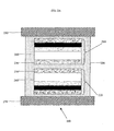
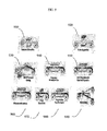
- FIG. 1 A multilayer HTS assembly according to one or more embodiments of the invention is shown in cross-section in FIG. 1 . It should be noted that in this and all subsequent figures, the dimensions are not to scale.
- Assembly 100 is made up of two HTS inserts 110 and 120. Each of these inserts is fabricated using techniques known in the art and that are described in greater detail below.
- Insert 110 includes a metal substrate 160. At least a surface of substrate 160 is biaxially textured to provide a crystal template for buffer layer 150 and HTS layer 140.
- One or more buffer layer(s) 150 is above substrate 160 and may comprise one or more layers.
- the buffer layer is made up of an electrically insulating material, though electrically conductive materials can be used.
- the buffer layer is made up of, e.g., an inert metal, an oxide, zirconate, titanate, niobate, nitride, tantalate, aluminate, cuprate, manganate, or ruthenate of a metal or rare earth element (e.g. Al 2 O 3 , CeO 2 , Y 2 O 3 , MgO, Gd 2 O 3 , strontium titanate, gadolinium zirconate, yttria-stabilized zirconia, AlN, Si 3 N 4 , LaMnO 4 , La 2 Zr 2 O 7 , or La 2-x Ce x Zr 2 O 7 .
- a metal or rare earth element e.g. Al 2 O 3 , CeO 2 , Y 2 O 3 , MgO, Gd 2 O 3 , strontium titanate, gadolinium zirconate, yttria-stabilized zirconia, AlN, Si 3 N 4
- HTS layer 140 is above buffer layer 150 may be any HTS material.
- the HTS layer includes a rare earth-alkaline earth-copper oxide, such as YBCO.
- Cap layer 130 is located above HTS layer 140 and provides protection of the HTS layer from chemical and mechanical degradation.
- the cap layer may be sputtered Ag or other inert metal.
- Insert 120 may have the identical or similar structure, including substrate 160', one or more buffer layer(s) 150', HTS layer 140', and cap layer 130'.
- respective wetting layers 170 and 170' can optionally be coated onto respective substrates 160 and 160'. These wetting layers facilitate the bonding of each insert to adhesive layer 180, and therefore facilitate the bonding of each insert to the other.
- adhesive layer 180 is made of solder.
- An exemplary solder is Pb-Sn-Ag.
- This oxide layer typically does not wet solder, i.e. does not bond to solder. It has been surprisingly discovered that the addition of Ag wetting layers 170 and 170' to substrates 160 and 160', respectively, makes the back surface wettable, i.e. bondable, to solder adhesive layer 180. Thus, bonding can be accomplished by soldering wetting layers that are bonded to the native oxide surfaces of the substrates.
- Deposition of Ag by DC sputtering is a standard operation.
- Translating coated conductor tape thought the plasma in a continuous mode without degradation of the superconductor properties requires cooling of the tape as it passes through the plasma.
- the tape is pulled across a cooling block that is positioned opposite the target to minimize the maximum temperature of the tape during deposition to bellow ⁇ 200 C.
- Proximity to the target may be required for adhesion of the Ag layer on the oxide surface.
- Energy imparted from the plasma likely cleans the deposition surface in situ and deposits the Ag ions with enough impact energy to make good physical contact.
- the electrically insulating native oxide layers on substrates 160 and 160' may be first removed. This removal can be done, e.g., by etching, electro-polishing, sputtering, or shot blasting. Then metallic wetting layers 170 and 170', e.g., Ag, Cu, Ni, Ti, or TiN, are coated onto the respective back surfaces of substrates 160 and 160' to prevent the regrowth of the native oxide on the substrate surfaces. Additionally these wetting layers 170, 170' promote adhesion of the bonding layer to the substrate surface. Then solder adhesive layer 180 bonds the two assemblies together. Rigorous removal of the native oxide layer is not required, however, in order to achieve electrical contact between inserts. As is described in greater detail below, the electrical conductive material that optionally surrounds the multilayer HTS assembly can provide additional current sharing.
- adhesive layer 180 is for example a resin, epoxy, or other non-conductive material, and wetting layers 170 and 170' are selected to facilitate bonding between substrates 160, 160', and the non-conducting adhesive layer. In this case it may be that some of the layers are conductive, and other layers are non-conductive. In applications where the desired adhesive wets the back substrate surfaces, wetting layers 170 and 170' can be eliminated entirely. In this case, adhesive layer 180 directly contacts substrates 160 and 160'.
- wetting layers 170 and 170' as well as adhesive layer 180 can be eliminated, in which case, the back surfaces of substrates 160 and 160' are brought directly into contact with each other.
- adhesive 180 bonds insert 110 to insert 120 at their respective substrates, creating HTS assembly 100.
- Cap layers 130 and 130' face outward in assembly 100, and substrates 160 and 160' are central to assembly 100.
- This configuration provides, for example, efficient electrical contact with an external current source, and efficient joining of lengths of superconductor wire.
- the outer surfaces of the assembly are electrically conductive cap layers 130 and 130'. These layers provide convenient electrically conductive paths to respective HTS layers 140 and 140'. In order to introduce current into the HTS layers, a connection between the current source and the assembly can be made anywhere on the outer surface of the assembly.
- FIG. 2A illustrates an embodiment of the present invention, having a wire 200 that includes two bonded HTS inserts 210, 220, which may be the same as previously described, and a conductive outer structure.
- the conductive outer structure substantially surrounds and seals the wire from the environment, and provides electrical contact between the two HTS inserts as well as to an external electrical contact.
- the conductive outer structure further provides mechanical, thermal, and electrical stabilization to wire 200.
- the conductive outer structure includes upper and lower conductive stabilizer strips 250, 270 and electrically conductive non-porous filler material 290, e.g. solder or another low-melting temperature alloy or amalgam, a conductive polymer, or a pure metal such as In.
- Filler 290 substantially surrounds HTS inserts 210, 220 and also may serve as bonding layer 180, illustrated in the HTS assembly 100 of FIG. 1 .
- substrates 260, 260' may be coated with respective wetting layers 230, 230' to enhance their bonding to filler 290 (and to each other).
- Filler 290 also bonds inserts 210, 220 to conductive stabilizer strips 250, 270 at the outer surfaces of the HTS inserts.
- Filler 290 bridges strips 250, 270 in thick layers on the sides of the wire to thereby complete the isolation of the HTS assembly from the surrounding environment and to substantially completely surround the HTS assembly in a conductive structure.
- HTS layer Occasionally there can be a defect within an HTS layer, which causes a corresponding increase in the resistance of (and heating in) the layer during use of the wire. In this case it can be useful to divert, or shunt, some or all of the current into another HTS layer. This results in a more uniform conductor, with a conductivity that does not vary greatly along the length of the wire. This is of particular use when the operating current is well below the critical current, a common practice in the operation of superconducting devices.
- a two HTS layer structure using a single substrate, having two HTS layers that are coated on opposing sides of the substrate, has been contemplated as a method of implementing multiple HTS layers in a single wire in order to provide redundant superconducting pathways.
- filler 290 provides electrical communication between the HTS inserts 210, 220.
- filler 290 behaves as a conductive conduit, or bridge.
- filler 290 is conductive, as current flows through wire 200, the current will generally follow the path of least resistance, which is through one or both HTS inserts 210, 220.
- one of HTS inserts 210, 220 has a defect that increases its resistance in a certain region, the current can flow through filler 290 into the other HTS insert.
- Filler 290 has a higher resistance than HTS inserts 210, 220, so the current transfers between the inserts over some calculable length (e.g. a few centimeters) of the wire.
- the net result of the transfer is that the current can continue traveling along a low resistance path, i.e. through the other HTS insert. If there is a defect at a different region in this insert, then the current can transfer back to the other insert, which is unlikely to also have a defect in the same place.
- the presence of redundant electrical pathways for the current improves the electrical stability of the wire.
- the current capacity of wire 200 is much less sensitive to local defects in either of HTS inserts 210, 220 than it would be with a single insert, where the current would be forced through a high resistance section of the wire.
- Filler 290 provides a means to introduce electrical current into one or both of HTS inserts 210, 220. By simply contacting a current source to filler 290, current flows via the filler into the HTS inserts. Because filler 290 is in contact with conductive stabilizer strips 250, 270, contacting a current source to one or both of strips250, 270 also introduces current to one or both of HTS inserts 210, 220.
- Material 290 is selected such that it is nonporous; in one or more embodiments, it is has sufficient strength and is coated with sufficient thickness to substantially surround and seal wire 200. This renders HTS inserts 210 and 220 substantially impervious to contamination by environmental factors, which can degrade the electrical performance of the inserts. Filler 290 may also substantially prevent infiltration of the assemblies by surrounding cryogenic fluid, which can form balloons that can potentially mechanically damage the HTS inserts. The thick coating of filler 290 on the sides of wire 200 also adds mechanical strength to the wire and may help to prevent delamination of wire 200 due to bending or other sources of potential damage. Material 290 adds thermal stability to the wire by providing additional heat capacity.
- Stabilizer strips 250 and 270 further enhance the mechanical, electrical, and thermal stability of wire 200.
- Strips 250, 270 can be the same or different, depending upon the desired characteristics of the resulting wire.
- the thickness of the strips can be varied throughout a wide range of about 0.01-2 mm, depending upon the desired application. For superconducting cables, the thickness is typically between 0.05-0.075 mm. For a fault current limiter application, the stabilizer thickness can be as high as or higher than 1 mm.
- the material used for strips 250 and 270 is selected to provide an appropriate electrical, thermal, and mechanical stability to wire 200 for the desired application.
- Strips 250 and 270 are generally a flexible conductive material, e.g. metal, e.g.
- stabilizer strips 250 and 270 have a width that is greater than the width of HTS inserts 210 and 220. This excess width, or overhang, allows layers or fillets of filler 290 to form along the sides of the wire by capillary action. In a preferred embodiment, the fillets have a concave profile relative to the edge of the wire. Because such fillets form by capillary action, the excess width of strips 250, 270 over the width of HTS assemblies 210, 220 determines the thickness of the fillet. Generally, the width of strips 250, 270 fall within the range of 0.01-2 mm greater than the width of HTS assemblies 210, 200.
- stabilizer strips with a width of about 4.3 mm can be used with 4.0 or 4.1 mm wide superconducting inserts. Fillets can enhance the mechanical strength and durability of wire 200. A wider fillet enhances strength, but reduces the engineering critical current density. An optimally designed wire will have sufficient filler width to meet the mechanical specifications, but not much more.
- a typical individual fillet width ranges from 0.025-0.2 mm, but can be higher or lower (e.g. 0.005-1 mm) to meet specific strength or engineering critical current needs.
- thick fillets of filler 290 enhance the mechanical strength of wire 200 because substrates 260, 260' may not bond well to solder due to their oxidation during insert processing, as described previously. While wetting layers (e.g. 230, 230') can be deposited on the substrate surfaces to improve their bonding to solder, depositing such a coating on the sides of the wire, e.g., on the exposed edges of the multilayer HTS inserts 210, 220, may not be practical because of increased production cost.
- wetting layers e.g. 230, 230'
- filler 290 can be deposited on the sides of wire 200, such that the filler adheres sufficiently to the other (non-substrate) layers of the multilayer assembly, and has sufficient strength, that it will not delaminate from the substrate sides.
- Some materials used as filler 290 e.g. Sn-Pb-Ag solders, strengthen considerably (up to three-fold) when cooled from room temperature to 77 K, and their contribution to the total strength can be significant.
- the fillet can be made appropriately thick.
- the following wire can be illustrative: a 40 mm wide conductor is, after completion of all buffer and superconductor deposition/reaction steps, coated on both sides with a 0.003 mm thick Ag layer using sputter deposition.
- the 40 mm wide conductor is slit in a reel to reel fashion into eight 4.1 mm wide inserts. Each insert is laminated in a reel-to-reel lamination process to a 0.05 x 4.3 mm copper 155 stabilizer strip on both sides, using a Sn-Pb solder to which some Ag can be added.
- the resulting wire varies in width between 4.3-4.4 mm.
- the solder fillet width is about 0.15-0.2 mm on average.
- Wire 200 may be manufactured as illustrated in FIG. 2B .
- HTS wire inserts are fabricated as wide (e.g. about 4 to 10 cm wide) multilayer strips and then slit lengthwise into several narrow (e.g. about 10 strips of about 0.4 cm wide, from a 4 cm wide strip) strips, which form HTS inserts 210, 220.
- Conductive stabilizer strips 250, 270 may be wider than the width of the narrow HTS strip, so that the stabilizer strips overhang the HTS strip on both sides.
- the wire is formed by joining narrow HTS insert strips 210, 220 with stabilizer strips 250, 270 in a bath of filler 290.
- Multilayer HTS inserts 210, 220 for example, may be fed into the filler bath from reels.
- Stabilizer strips 250, 270 may be fed off reels placed above and below the feed-in reels of HTS inserts 210, 220 so that the lengths of material form a stacked configuration.
- the filler simultaneously surrounds HTS inserts 210, 220 and also laminates them to the conductive stabilizer strips 250, 270.
- Die 295 merges and consolidates inserts 210, 220 and stabilizer strips 250, 270 into one superconducting wire 200.By laminating the stabilizer strips to the wire after fabricating and slitting the HTS inserts, the stabilizer strips can easily be made wider than the inserts.
- the overhanging feature promotes the capillary wicking of the solder between the upper and lower stabilizer strips 250, 270 to provide thick, mechanically robust fillets of filler 290 on the sides of the wire.
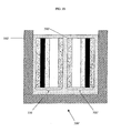
- FIG. 3A shows another embodiment of the present invention, having wire 300 that includes an HTS assembly including two bonded HTS inserts 310, 320, which may be the same as previously described, and a conductive outer structure.
- the conductive outer structure includes a first component 350 covering 3 sides of the HTS assembly, e.g., a three-walled trough, which can be assembled, a single part, or in a plurality of pieces, and electrically conductive non-porous filler 390.
- Filler 390 e.g., solder, surrounds inserts 310, 320 and bonds them together at their substrates as previously described.
- Filler 390 provides an electrical pathway between three-sided component 350 and HTS inserts 310, 320, and also between the inserts.
- Filler 390 seals inserts 310, 320 into three-sided component350.
- Three-sided component 350 is made from a flexible conductive material, e.g. metal, e.g. aluminum, copper, silver, nickel, iron, stainless steel, aluminum alloy, copper alloy, silver alloy, nickel alloy, nickel tungsten alloy, or iron alloy. As described above for stabilizer strips 250 and 270 in FIG. 2A , the material for three-sided component 350 is selected to provide electrical, thermal, and mechanical stability to the wire for the desired application.
- the walls of the three-sided component can have a thickness between, for example, 0.0001-0.5 mm, and can be thicker depending on the desired application (e.g. 0.0001-1 mm).
- Three-sided component 350 has a width that is wider than inserts 310 and 320, and a depth that is deeper than the thickness of the HTS assembly.
- Wire 300 is manufactured by first providing HTS inserts 310, 320, which can be slit from wide strips as described previously. Then in a bath of filler 390, e.g. solder, inserts 310, 320 are simultaneously bonded together, surrounded by filler 390, inserted into three-sided component 350, and sealed into the three-sided component.
- filler 390 e.g. solder
- FIG. 3B shows a wire having an alternate arrangement of two bonded HTS inserts 310', 320', which may be the same as previously described, that are sealed inside of three-sided component 350'.
- Electrically conductive non-porous filler 390' e.g., solder, substantially surrounds inserts 310' and 320' and bonds them together at their substrates.
- Filler 390' provides an electrical pathway to and between HTS inserts 310', 320'.
- Filler 390' seals inserts 310', 320' into three-sided component350', which may be the same as described previously.
- three-sided component 350' has a width that is wider than the thickness of the assembly, and a depth that is deeper than the width of the assembly. This allows for a sufficiently thick layer of filler 390' to substantially surround the assembly on all sides and to substantially seal wire 300'.
- Wire 300' may be manufactured as described for FIG. 3A .
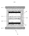
- FIG. 4A shows a wire 400 having HTS inserts 410, 420, which may be the same as previously described, that are sealed inside of a four-walled structure 450, which may provide additional mechanical stability over the three-walled trough of FIGS. 3A and 3B .
- Electrically conductive non-porous filler 490 e.g., solder, surrounds inserts 410, 420 and bonds them together at their substrates as previously described.
- Filler 490 provides an electrical pathway to and between HTS inserts 410,420.
- Filler 490 seals inserts 410, 420 into four-walled structure 450.
- the internal dimensions of structure 450 are larger than the appropriate dimensions of bonded HTS inserts 410 and 420.
- Wire 400 can manufactured by first providing the HTS inserts, which can be slit from wide strips as described previously. One of the walls of structure 450 is left open in order to leave an adequate space to receive HTS inserts 410 and 420. In a solder bath, the inserts are then simultaneously inserted into structure 450, bonded together, and surrounded by solder. The open wall of structure 450 is then mechanically folded over, enclosing the inserts and solder. Solder fills the gap left from the fold, as can be seen in the figure.
- FIG. 4B shows a wire 400' having an alternate arrangement of two bonded HTS inserts 410', 420', which may be the same as previously described, that are sealed inside of four-walled structure 450'.
- Electrically conductive non-porous filler 490' e.g., solder, surrounds inserts 410', 420' and bonds them together at their substrates as previously described.
- Filler 490' provides an electrical pathway to and between HTS inserts 410', 420'.
- Filler 490' seals inserts 410', 420' into four-walled structure 450'.
- the internal dimensions of structure 450' are larger than the appropriate dimensions of bonded HTS inserts 410', 420'. This allows for a sufficiently thick layer of solder to surround the inserts on all sides and seal the structure.
- Wire 400' may be manufactured as described for FIG. 4A .
- a thin conductive foil is wrapped around an HTS assembly.
- adhesive 580 bonds together HTS inserts 510, 520, which may be the same as previously described.
- Conductive foil 590 is tightly and contiguously wrapped around the bonded inserts. This places foil 590 in good electrical contact with inserts 510, 520, and provides a route for electrical communication between the inserts.
- FIG. 5B each consecutive wrap of foil 590' around inserts 510', 520' overlaps with the previous wrap, providing a seal around the wire.
- Substantially nonporous sealer 570 is coated on top of foil 590.
- Sealer 570 can be a electrically conductive material, in which case sealer 570 and foil 590 together provide an electrical pathway from the outside of the wire to HTS inserts 510, 520.
- sealer 570 can be a substantially nonporous non-conductive material, in which case the exterior of wire 500 is electrically insulated. In this case to make a conductive connection from the outside of wire 500 to HTS inserts 510, 520, sealer 570 must be stripped away.
- Wire 500 can be manufactured by providing and bonding HTS inserts 510, 520 as described previously, and then mechanically wrapping conductive foil 590 around the resulting assembly. Then wire 500 can be run through a bath of sealer 570, e.g. solder, which substantially surrounds and seals wire 500.
- sealer 570 e.g. solder
- wire 600 includes two HTS inserts 610, 620, which are bonded with adhesive 680 and may be the same as described previously, layer 690, and a two-tape structure like that shown in FIG. 2A .
- Layer 690 substantially surrounds and provides electrical contact between 610, 620, 680.
- Layer 690 is, for example, a metallic coating that is deposited onto assembly 610, 620, 680.
- Cu, Ag, Ti, TiN, and Sn are examples of metals that can be deposited onto the assembly.
- layer 690 is e.g, a coating of a conductive polymer, a polymer containing metallic powder, or conductive glue, to result in a conductive medium.
- conductive stabilizer strips 650, 660 are laminated to the assembly with filler 670 as described for the wire shown in FIG. 2 .
- Filler 670 may be the same as described for FIG. 2 .
- Stabilizer strips 650, 660, along with filler 670, provide structural, thermal, and electrical integrity to wire 600 beyond that provided by layer 690. Because wire 600 contains many features that enhance its strength and durability, it is useful for applications with harsh environmental conditions or excessive mechanical stress.
- the coated assembly 610, 620, 680, 690 can also be inserted in any of the above-described embodiments, for applications requiring additional stability.
- a wire in one or more embodiments of the present invention, as illustrated in FIG. 7 , includes two HTS inserts 710, 720, which are bonded with adhesive 780 and may be the same as described previously, and an electrically conductive layer 790.
- Layer 790 may substantially surround and seal the HTS assembly 710, 720, 780.
- Layer 790 provides electrical communication between HTS inserts 710, 720.
- Layer 790 can be a deposited metal coating. The metal can be deposited by an electroplating process, by a metal powder sintering process, or by an electroless plating process. Electroplating, powder sintering, and electroless plating methods are well known.
- layer 790 is a conductive polymer, or a polymer containing metallic powder.
- Polymer coatings can be applied through a reel-to-reel dip coating and curing process, with dies or wipes in-line to control the polymer layer thickness.
- Still other kinds of conductive materials can be used for layer 790. These materials have the property of providing good electrical contact between HTS inserts 710, 720 and/or between HTS inserts 710, 720 and an external conductive contact. These materials also can be substantially nonporous, and can be deposited with a thickness sufficient to substantially surround and seal the resulting wire 700.
- wires that include HTS inserts that are bonded together by their substrates, and inserted inside of different kinds of outer structures other HTS assemblies can be contemplated for use in any of the described wires.
- the coated wire 700 of FIG. 7 can itself be inserted into one or more of the described outer conductive structures.
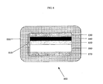
- wire 800 includes an HTS insert 810 that may be the same as described previously.
- Wire 800 also includes an outer structure 890, where outer structure 890 represents the outer conductive structure of any of the embodiments illustrated in FIGS. 2-7 .
- HTS insert 810 includes substrate 860, buffer layer 850, HTS layer 840, and cap layer 830, which may have the same components and characteristics as insert 110 in the configuration shown in FIG. 1 .
- Insert 810 also has a wetting layer 870 that is deposited on substrate 860.
- wetting layer 870 is selected such that it allows for good adhesion between substrate 860 and outer structure 890.
- Outer structure 890 is in electrical contact with HTS layer 840. Thus by simply contacting a current source to outer structure 890, current will flow into the HTS layer. Outer structure 890 substantially surrounds and seals HTS insert 810.
- the wires contain HTS inserts and assemblies having a substrate, one or more buffer layer (s), rare earth oxide superconductor, and cap layer, the wires are not constrained to using these specific kinds of superconductor inserts or assemblies.
- Any kind of HTS assembly can be used, provided that it contains an HTS layer.
- a mesh-type stabilizer having low conductivity in the weft (perpendicular to the wire axis) and high conductivity in the warp (along the wire axis) can be used in place of conductive stabilizer strips. This type of stabilizer has the advantage of reducing eddy current losses in alternating current applications. Further details of appropriate mesh-type stabilizers may be found in commonly-owned U.S. Patent Application, U.S.S.N. 60/667,001 and published as US 2006/0394917 A1 , entitled "Mesh-Type Stabilizer for Filamentary Coated Superconductors,".
- Fig. 9 illustrates a flow diagram of an exemplary process used to manufacture an HTS wire according to various embodiments of the present invention.
- a wire substrate is treated to obtain biaxial texture.
- the substrate surface has a relatively well defined crystallographic orientation.
- the surface can be a biaxially textured surface (e.g., a (113)[211] surface) or a cube textured surface (e.g., a (100)[011] surface or a (100)[001] surface).
- the peaks in an X-ray diffraction pole figure of the surface have a FWHM of less than about 20° (e.g., less than about 15°, less than about 10°, or from about 5° to about 10°).
- the surface can be prepared, for example, by rolling and annealing.
- Surfaces can also be prepared using vacuum processes, such as ion beam assisted deposition, inclined substrate deposition and other vacuum techniques known in the art to form a biaxially textured surface on, for example, a randomly oriented polycrystalline or amorphous surface.
- the surface of the substrate need not be textured (e.g., the surface can be randomly oriented polycrystalline, or the surface can be amorphous).
- the substrate can be formed of any material capable of supporting a buffer layer stack and/or a layer of superconductor material, and capable of providing the mechanical properties required for the final wire.
- substrate materials that can be used as the substrate include for example, metals and/or alloys, such as nickel, silver, copper, zinc, aluminum, iron, chromium, vanadium, palladium, molybdenum and/or their alloys.
- the substrate can be formed of a superalloy.
- the substrate can be in the form of an object having a relatively large surface area (e.g., a wire or a wafer). In these embodiments, the substrate is preferably formed of a relatively flexible material.
- the substrate is a binary alloy that contains two of the following metals: copper, nickel, chromium, vanadium, aluminum, silver, iron, palladium, molybdenum, tungsten, gold and zinc.
- a binary alloy can be formed of nickel and chromium (e.g., nickel and at most 20 atomic percent chromium, nickel and from about five to about 18 atomic percent chromium, or nickel and from about 10 to about 15 atomic percent chromium).
- a binary alloy can be formed of nickel and copper (e.g., copper and from about five to about 45 atomic percent nickel, copper and from about 10 to about 40 atomic percent nickel, or copper and from about 25 to about 35 atomic percent nickel).
- a binary alloy can contain nickel and tungsten (e.g., from about one atomic percent tungsten to about 20 atomic percent tungsten, from about two atomic percent tungsten to about 10 atomic percent tungsten, from about three atomic percent tungsten to about seven atomic percent tungsten, about five atomic percent tungsten).
- a binary alloy can further include relatively small amounts of impurities (e.g., less than about 0.1 atomic percent of impurities, less than about 0.01 atomic percent of impurities, or less than about 0.005 atomic percent of impurities).
- Ni-5wt.%W is a preferred material for the substrate.
- the substrate contains more than two metals (e.g., a ternary alloy or a quarternary alloy).
- the alloy can contain one or more oxide formers (e.g., Mg, Al, Mo, V, Ta, Ti, Cr, Ga, Ge, Zr, Hf, Y, Si, Pr, Eu, Gd, Tb, Dy, Ho, Lu, Th, Er, Tm, Be, Ce, Nd, Sm, Yb and/or La, with Al being the preferred oxide former), as well as two of the following metals: copper, nickel, chromium, tungsten, vanadium, aluminum, silver, iron, palladium, molybdenum, gold and zinc.
- oxide formers e.g., Mg, Al, Mo, V, Ta, Ti, Cr, Ga, Ge, Zr, Hf, Y, Si, Pr, Eu, Gd, Tb, Dy, Ho, Lu, Th, Er, Tm, Be, Ce, Nd, Sm, Yb and/or La,
- the alloy can contain two of the following metals: copper, nickel, chromium, tungsten, vanadium, aluminum, silver, iron, palladium, molybdenum, gold and zinc, and can be substantially devoid of any of the aforementioned oxide formers.
- the alloys can contain at least about 0.5 atomic percent oxide former (e.g., at least about one atomic percent oxide former, or at least about two atomic percent oxide former) and at most about 25 atomic percent oxide former (e.g., at most about 10 atomic percent oxide former, or at most about four atomic percent oxide former).
- the alloy can include an oxide former (e.g., at least about 0.5 aluminum), from about 25 atomic percent to about 55 atomic percent nickel (e.g., from about 35 atomic percent to about 55 atomic percent nickel, or from about 40 atomic percent to about 55 atomic percent nickel) with the balance being copper.
- the alloy can include an oxide former (e.g., at least about 0.5 atomic aluminum), from about five atomic percent to about 20 atomic percent chromium (e.g., from about 10 atomic percent to about 18 atomic percent chromium, or from about 10 atomic percent to about 15 atomic percent chromium) with the balance being nickel.
- the alloys can include relatively small amounts of additional metals (e.g., less than about 0.1 atomic percent of additional metals, less than about 0.01 atomic percent of additional metals, or less than about 0.005 atomic percent of additional metals).
- a substrate formed of an alloy can be produced by, for example, combining the constituents in powder form, melting and cooling or, for example, by diffusing the powder constituents together in solid state.
- the alloy can then be formed by deformation texturing (e.g, annealing and rolling, swaging, extrusion and/or drawing) to form a textured surface (e.g., biaxially textured or cube textured).
- deformation texturing e.g, annealing and rolling, swaging, extrusion and/or drawing
- the alloy constituents can be stacked in a jelly roll configuration, and then deformation textured.
- a material with a relatively low coefficient of thermal expansion e.g, Nb, Mo, Ta, V, Cr, Zr, Pd, Sb, NbTi, an intermetallic such as NiAl or Ni 3 Al, or mixtures thereof
- a material with a relatively low coefficient of thermal expansion e.g, Nb, Mo, Ta, V, Cr, Zr, Pd, Sb, NbTi, an intermetallic such as NiAl or Ni 3 Al, or mixtures thereof
- an intermetallic such as NiAl or Ni 3 Al, or mixtures thereof
- stable oxide formation at the surface can be mitigated until a first epitaxial (for example, buffer) layer is formed on the biaxially textured alloy surface, using an intermediate layer disposed on the surface of the substrate.
- Intermediate layers include those epitaxial metal or alloy layers that do not form surface oxides when exposed to conditions as established by PO 2 and temperature required for the initial growth of epitaxial buffer layer films.
- the buffer layer acts as a barrier to prevent substrate element(s) from migrating to the surface of the intermediate layer and forming oxides during the initial growth of the epitaxial layer. Absent such an intermediate layer, one or more elements in the substrate would be expected to form thermodynamically stable oxide(s) at the substrate surface which could significantly impede the deposition of epitaxial layers due to, for example, lack of texture in this oxide layer.
- Exemplary intermediate metal layers include nickel, gold, silver, palladium, and alloys thereof. Additional metals or alloys may include alloys of nickel and/or copper.
- Epitaxial films or layers deposited on an intermediate layer can include metal oxides, chalcogenides, halides, and nitrides. In some embodiments, the intermediate metal layer does not oxidize under epitaxial film deposition conditions.
- the deposited intermediate layer is not completely incorporated into or does not completely diffuse into the substrate before nucleation and growth of the initial buffer layer structure causes the epitaxial layer to be established. This means that after selecting the metal (or alloy) for proper attributes such as diffusion constant in the substrate alloy, thermodynamic stability against oxidation under practical epitaxial buffer layer growth conditions and lattice matching with the epitaxial layer, the thickness of the deposited metal layer has to be adapted to the epitaxial layer deposition conditions, in particular to temperature.
- Deposition of the intermediate metal layer can be done in a vacuum process such as evaporation or sputtering, or by electro-chemical means such as electroplating (with or without electrodes). These deposited intermediate metal layers may or may not be epitaxial after deposition (depending on substrate temperature during deposition), but epitaxial orientation can subsequently be obtained during a post-deposition heat treatment.
- sulfur can be formed on the surface of the substrate or intermediate layer.
- the sulfur can be formed, for example, by exposing the intermediate layer to a gas environment containing a source of sulfur (e.g., H 2 S, a tantalum foil or a silver foil) and hydrogen (e.g., hydrogen, or a mix of hydrogen and an inert gas, such as a 5% hydrogen/argon gas mixture) for a period of time (e.g., from about 10 seconds to about one hour, from about one minute to about 30 minutes, from about five minutes to about 15 minutes).
- a source of sulfur e.g., H 2 S, a tantalum foil or a silver foil
- hydrogen e.g., hydrogen, or a mix of hydrogen and an inert gas, such as a 5% hydrogen/argon gas mixture
- This can be performed at elevated temperature (e.g., at a temperature of from about 450°C to about 1100°C, from about 600°C to about 900°C, 850°C).
- the pressure of the hydrogen can be relatively low (e.g., less than about 133Pa (one torr), less than about 133 x 10 -3 Pa (1x10 -3 torr), less than about 133 x 10 -6 Pa (1x10 -6 torr)) or relatively high (e.g., greater than about 0.133kPa (1 torr), greater than about 13.3kPa (100 torr), greater than about 101.3kPa (760 torr)).
- exposing the textured substrate surface to a source of sulfur under these conditions can result in the formation of a superstructure (e.g., a c(2x2) superstructure) of sulfur on the textured substrate surface. It is further believed that the superstructure can be effective in stabilizing (e.g., chemically and/or physically stabilizing) the surface of the intermediate layer.
- a superstructure e.g., a c(2x2) superstructure
- the superstructure can be effective in stabilizing (e.g., chemically and/or physically stabilizing) the surface of the intermediate layer.
- a sulfur superstructure e.g., S c(2x2)
- S c(2x2) can be formed by applying an appropriate organic solution to the surface of the intermediate layer by heating to an appropriate temperature in an appropriate gas environment.
- formation of a sulfur superstructure on the surface of the intermediate layer has been described, it is believed that other superstructures may also be effective in stabilizing (e.g., chemically and/or physically stabilizing) the surface.
- an oxygen superstructure, a nitrogen superstructure, a carbon superstructure, a potassium superstructure, a cesium superstructure, a lithium superstructure or a selenium superstructure disposed on the surface may be effective in enhancing the stability of the surface.
- a buffer layer is formed on the textured substrate by epitaxial growth on a textured metal surface.
- a buffer layer can be formed on a polycrystalline, randomly textured metal surface using ion beam assisted deposition (IBAD).
- IBAD ion beam assisted deposition
- a buffer layer material is evaporated using, for example, electron beam evaporation, sputtering deposition, or pulsed laser deposition while an ion beam (e.g., an argon ion beam) is directed at a smooth amorphous surface of a substrate onto which the evaporated buffer layer material is deposited.
- the buffer layer can be formed by ion beam assisted deposition by evaporating a buffer layer material having a rock-salt like structure (e.g., a material having a rock salt structure, such as an oxide, including MgO, or a nitride) onto a smooth, amorphous surface (e.g., a surface having a root mean square roughness of less than about 100 Angstroms) of a substrate so that the buffer layer material has a surface with substantial alignment (e.g., about 13° or less), both in-plane and out-of-plane.
- a buffer layer material having a rock-salt like structure e.g., a material having a rock salt structure, such as an oxide, including MgO, or a nitride
- a smooth, amorphous surface e.g., a surface having a root mean square roughness of less than about 100 Angstroms
- the conditions used during deposition of the buffer layer material can include, for example, a substrate temperature of from about 0°C to about 750°C (e.g., from about 0°C to about 400°C, from about room temperature to about 750°C, from about room temperature to about 400°C), a deposition rate of from about 0.1nm (1.0 Angstrom) per second to about 0.44nm (4.4 Angstroms) per second, an ion energy of from about 200 eV to about 1200 eV, and/or an ion flux of from about 110 microamperes per square centimeter to about 120 microamperes per square centimeter.
- a substrate temperature of from about 0°C to about 750°C (e.g., from about 0°C to about 400°C, from about room temperature to about 750°C, from about room temperature to about 400°C)
- a deposition rate of from about 0.1nm (1.0 Angstrom) per second to about 0.44nm (4.4 Angstroms)
- the substrate when using IBAD, is formed of a material having a polycrystalline, non-amorphous base structure (e.g., a metal alloy, such as a nickel alloy) with a smooth amorphous surface formed of a different material (e.g., Si 3 N 4 ).
- a material having a polycrystalline, non-amorphous base structure e.g., a metal alloy, such as a nickel alloy
- a smooth amorphous surface formed of a different material e.g., Si 3 N 4
- a plurality of buffer layers can be deposited by epitaxial growth on an original IBAD surface.
- Each buffer layer can have substantial alignment (e.g., about 13° or less), both in-plane and out-of-plane.
- a buffer material can be prepared using solution phase techniques, including metalorganic deposition, such as disclosed in, for example, S.S. Shoup et al., J. Am. Cer. Soc., vol. 81, 3019 ; D. Beach et al., Mat. Res. Soc. Symp. Proc., vol. 495, 263 (1988 ); M. Paranthaman et al., Superconductor Sci. Tech., vol. 12, 319 (1999 ); D.J. Lee et al., Japanese J. Appl. Phys., vol. 38, L178 (1999 ) and M.W. Rupich et al., I.E.E.E. Trans. on Appl. Supercon. vol. 9, 1527 .
- solution coating processes can be used for epitaxial deposition of one or a combination of any of the oxide layers on textured substrates; however, they can be particularly applicable for deposition of the initial (seed) layer on a textured metal substrate.
- the role of the seed layer is to provide 1) protection of the substrate from oxidation during deposition of the next oxide layer when carried out in an oxidizing atmosphere relative to the substrate (for example, magnetron sputter deposition of yttria-stabilized zirconia from an oxide target); and 2) an epitaxial template for growth of subsequent oxide layers.
- the seed layer should grow epitaxially over the entire surface of the metal substrate and be free of any contaminants that may interfere with the deposition of subsequent epitaxial oxide layers.
- oxide buffer layers can be carried out so as to promote wetting of an underlying substrate layer.
- formation of metal oxide layers can be carried out using metal alkoxide precursors (for example, "sol gel" precursors).
- a precursor solution is deposited at deposition station 930 as described above.
- the precursor can be patterned. Additional equipment may be required to accomplish the patterning operation, for example, when laser ablation or ion bombardment are used to pattern the superconducting layer. If dropwise patterned deposition is used, then a single station equipped with a inkjet printer deposition apparatus can accomplish both deposition and patterning of the oxide precursor solution.
- solution chemistry is used to prepare barium fluoride and/or other superconductor precursors; and a solution (e.g., a solution containing metal salts, such as yttrium acetate, copper acetate, barium acetate and/or a fluorinated acetate salt of barium) is disposed on a surface (e.g., on a surface of a substrate, such as a substrate having an alloy layer with one or more buffer layers disposed thereon).
- the solution can be disposed on the surface using standard techniques (e.g., spin coating, dip coating, slot coating).
- the solution is dried to remove at least some of the organic compounds present in the solution (e.g., dried at about room temperature or under mild heat), and the resulting material is reacted (e.g., decomposed) in a furnace in a gas environment containing oxygen and water to form barium fluoride and/or other appropriate materials (e.g., CuO and/or Y 2 O 3 ).
- the reactors noted above can be used in any or all of these steps.
- Metal salt solutions are prepared using metal sources in the appropriate proportions desired in the resulting superconductor layer.
- the precursor solution may contain additive components, including soluble and insoluble metal compounds, that are used to modify the final superconductor composition.
- Such additives can include, for example, soluble compounds of metal compounds such as yttrium, neodymium, samarium, europium, gadolinium, terbium, dysprosium, holmium, erbium, thulium, ytterbium, and lutetium, alkaline earth metals, such as calcium, manganese, iron, cobalt, nickel, zirconium, cerium, silver, aluminum, and magnesium, that are capable of dissolving in the solvents contained in the precursor solution.
- Additive components may also include stoichiometric excesses of soluble compounds included in the precursor solution. For example, soluble yttrium salts or soluble copper salts may be included in the precursor solution in excess of that required to form YBCO. Insoluble additive components can also be added to the precursor solution.
- metal salt solutions that can be used are as follows.
- the metal salt solution can have a relatively small amount of free acid. In aqueous solutions, this can correspond to a metal salt solution with a relatively neutral pH (e.g., neither strongly acidic nor strongly basic).
- the metal salt solution can be used to prepare multi-layer superconductors using a wide variety of materials that can be used as the underlying layer on which the superconductor layer is formed.
- the total free acid concentration of the metal salt solution can be less than about 1x10 -3 molar (e.g., less than about 1x10 -5 molar or about 1x10 -7 molar).
- free acids that can be contained in a metal salt solution include trifluoroacetic acid, acetic acid, nitric acid, sulfuric acid, acids of iodides, acids of bromides and acids of sulfates.
- the precursor composition can have a pH of at least about 3 (e.g., at least about 5 or about 7).
- the metal salt solution can have a relatively low water content (e.g., less than about 50 volume percent water, less than about 35 volume percent water, less than about 25 volume percent water).
- the total amount of trifluoroacetate ion can be selected so that the mole ratio of fluorine contained in the metal salt solution (e.g., in the form of trifluoroacetate) to the alkaline earth metal (e.g., barium ions) contained in the metal salt solution is at least about 2:1 (e.g., from about 2:1 to about 18.5:1, or from about 2:1 to about 10:1).
- the metal salt solution can be prepared by combining soluble compounds of a first metal (e.g., copper), a second metal (e.g., an alkaline earth metal), and a rare earth metal with one or more desired solvents and optionally water.
- soluble compounds of the first, second and rare earth metals refer to compounds of these metals that are capable of dissolving in the solvent(s) contained in the metal salt solution.
- Such compounds include, for example, salts (e.g., nitrates, acetates, alkoxides, iodides, sulfates and trifluoroacetates), oxides and hydroxides of these metals.
- a metal salt solution can be formed of an organic solution containing metal trifluoroacetates prepared from powders of Ba(O 2 CCH 3 ) 2 , Y(O 2 CCH 3 ) 3 , and Cu(O 2 CCH 3 ) 2 which are combined and reacted using methods known to those skilled in the art.
- the metal trifluoroacetate powders can be combined in a 2:1:3 ratio in methyl alcohol to produce a solution substantially 0.94 M based on copper content.
- the metal salt solution can contain a Lewis base.
- the rare earth metal can be yttrium, lanthanum, europium, gadolinium, terbium, dysprosium, holmium, erbium, thulium, ytterbium, cerium, praseodymium, neodymium, promethium, samarium or lutetium.
- the rare earth metal salt can be any rare earth metal salt that is soluble in the solvent(s) contained in the metal salt solution and that, when being processed to form an intermediate (e.g., a metal oxyhalide intermediate), forms rare earth oxide(s) (e.g., Y 2 O 3 ).
- Such salts can have, for example, the formula M(O 2 C-(CH 2 ) n -CXX'X")(O 2 C-(CH 2 ) m -CX'"X""X""')(O 2 C-(CH 2 ) p -CX"""X"""') or M(OR) 3 .
- M is the rare earth metal.
- n, m and p are each at least one but less than a number that renders the salt insoluble in the solvent(s) (e.g., from one to ten).
- R is a carbon containing group, which can be halogenated (e.g., CH 2 CF 3 ) or nonhalogenated.
- halogenated e.g., CH 2 CF 3
- salts include nonhalogenated carboxylates, halogenated acetates (e.g., trifluoroacetate, trichloroacetate, tribromoacetate, triiodoacetate), halogenated alkoxides, and nonhalogenated alkoxides.
- nonhalogenated carboxylates examples include nonhalogenated actetates (e.g., M(O 2 C-CH 3 ) 3 ).
- the alkaline earth metal can be barium, strontium or calcium.
- the alkaline earth metal salt can be any alkaline earth metal salt that is soluble in the solvent(s) contained in the metal salt solution and that, when being processed to form an intermediate (e.g., a metal oxyhalide intermediate), forms an alkaline earth halide compound (e.g., BaF 2 , BaCl 2 , BaBr 2 , BaI 2 ) prior to forming alkaline earth oxide(s) (e.g., BaO).
- Such salts can have, for example, the formula M'(O 2 C-(CH 2 ) n -CXX'X")(O 2 C-(CH 2 ) m -CX"'X""X”"') or M'(OR) 2 .
- M' is the alkaline earth metal.
- n and m are each at least one but less than a number that renders the salt insoluble in the solvent(s) (e.g., from one to ten).
- Each of X, X', X", X"', X"" and X'”” is H, F, Cl, B or, I.
- R can be a halogenated or nonhalogenated carbon containing group.
- halogenated acetates e.g., trifluoroacetate, trichloroacetate, tribromoacetate, triiodoacetate.
- the transition metal is copper.
- the transition metal salt should be soluble in the solvent(s) contained in the metal salt solution.
- minimal cross-linking occurs between discrete transition metal molecules (e.g., copper molecules).
- Such transition metals salts can have, for example, the formula M"(CXX'X"-CO(CH) a CO-CX"'X"X""')(CX"""X"""'X""""-CO(CH) b CO CX"""'X"""""""""""), M"(O 2 C-(CH 2 ) n -CXX'X") (O 2 C-(CH 2 ) m -CX"'X""""') or M"(OR) 2 .
- M" is the transition metal.
- a and b are each at least one but less than a number that renders the salt insoluble in the solvent(s) (e.g., from one to five).
- n and m are each at least one but less than a number that renders the salt insoluble in the solvent(s) (e.g., from one to ten).
- Each of X, X', X", X"', X"", X"", X""', X""", X"""", X"""', X"""", X""""""" is H, F, Cl, Br or I.
- R is a carbon containing group, which can be halogenated (e.g., CH 2 CF 3 ) or nonhalogenated.
- salts include, for example, nonhalogenated actetates (e.g., M"(O 2 C-CH 3 ) 2 ), halogenated acetates, halogenated alkoxides, and nonhalogenated alkoxides.
- salts include copper trichloroacetate, copper tribromoacetate, copper triiodoacetate, Cu(CH 3 COCHCOCF 3 ) 2 , Cu(OOCC 7 H 15 ) 2 , Cu(CF 3 COCHCOF 3 ) 2 , Cu(CH 3 COCHCOCH 3 ) 2 , Cu(CH 3 CH 2 CO 2 CHCOCH 3 ) 2 , CuO(C 5 H 6 N) 2 and Cu 3 O 3 Ba 2 (O-CH 2 CF 3 ) 4 .
- the transition metal salt is a carboxylate salt (e.g., a nonhalogenated carboxylate salt), such as a propionate salt of the transition metal (e.g., a nonhalogenated propionate salt of the transition metal).
- a nonhalogenated propionate salt of a transition metal is Cu(O 2 CC 2 H 5 ) 2 .
- the transition metal salt is a simple salt, such as copper sulfate, copper nitrate, copper iodide and/or copper oxylate.
- n and/or m can have the value zero.
- a and/or b can have the value zero.
- Lewis bases includes nitrogen-containing compounds, such as ammonia and amines.
- amines include CH 3 CN, C 5 H 5 N and R 1 R 2 R 3 N.
- R 1 R 2 R 3 is independently H, an alkyl group (e.g., a straight chained alkyl group, a branched alkyl group, an aliphatic alkyl group, a non-aliphatic alkyl group and/or a substituted alkyl group) or the like.
- an alkyl group e.g., a straight chained alkyl group, a branched alkyl group, an aliphatic alkyl group, a non-aliphatic alkyl group and/or a substituted alkyl group
- the metal salt solution is applied to a surface (e.g., a buffer layer surface), such as by spin coating, dip coating, web coating, slot coating, gravure coating, or other techniques known to those skilled in the art, and subsequently heated.
- a surface e.g., a buffer layer surface
- the precursor components are decomposed.
- the first step of the heating step is performed to decompose the metalorganic molecules to one or more oxyfluoride intermediates of the desired superconductor material.
- the initial temperature in this step is about room temperature, and the final temperature is from about 190°C to about 210°C, preferably to a temperature to about 200°C.
- this step is performed using a temperature ramp of at least about 5°C per minute, more preferably a temperature ramp of at least about 10°C per minute, and most preferably a temperature ramp of at least about 15°C per minute.
- the partial pressure of water vapor in the nominal gas environment is preferably maintained at from about 666.6Pa (5 Torr) to about 6.67kPa (50 Torr), more preferably at from about 666.6Pa (5 Torr) to about 4kPa (30 Torr), and most preferably at from about 2.67kPa (20 Torr) to about 4kPa (30 Torr).
- the partial pressure of oxygen in the nominal gas environment is maintained at from about 13.3Pa (0.1 Torr) to about 101.3kPa (760 Torr) and preferably at about 97.3 - 98.7kPa (730 - 740 Torr).
- Heating is then continued to a temperature of from about 200°C to about 290°C using a temperature ramp of from about 0.05°C per minute to about 5°C per minute (e.g., from about 0.5°C per minute to about 1°C per minute).
- the gas environment during this heating step is substantially the same as the nominal gas environment used when the sample is heated to from the initial temperature to from about 190°C to about 215°C.
- Heating is further continued to a temperature of about 650°C, or more preferably to a temperature of about 400°C, to form the oxyfluoride intermediate.
- This step is preferably performed using a temperature ramp of at least about 2°C per minute, more preferably at least about 3°C per minute, and most preferably at least about 5°C per minute.
- the gas environment during this heating step is substantially the same as the nominal gas environment used when the sample is heated to from the initial temperature to from about 190°C to about 215°C.
- barium fluoride is formed by heating the dried solution from an initial temperature (e.g., room temperature) to a temperature of from about 190°C to about 215°C (e.g., about 210°C) in a water vapor pressure of from about 666.6Pa (5 Torr) to about 6.67kPa (50 Torr) water vapor (e.g., from about 666.6Pa (5 Torr) to about 4kPa (30 Torr) water vapor, or from about 1.3kPa (10 Torr) to about 3.3kPa (25 Torr) water vapor).
- the nominal partial pressure of oxygen can be, for example, from about 13.3Pa (0.1 Torr) to about 101.3kPa (760 Torr).
- heating is then continued to a temperature of from about 220°C to about 290°C (e.g., about 220°C) in a water vapor pressure of from about 666.6Pa (5 Torr) to about 6.67kPa (50 Torr) water vapor (e.g., from about 666.6Pa (5 Torr) to about 4kPa (30 Torr) water vapor, or from about 1.3kPa (10 Torr) to about 3.3kPa (25 Torr) water vapor).
- the nominal partial pressure of oxygen can be, for example, from about 13.3Pa (0.1 Torr) to about 101.3kPa (760 Torr).
- the nominal partial pressure of oxygen can be, for example, from about 13.3Pa (0.1 Torr) to about 101.3kPa (760 Torr).
- heating the dried solution to form barium fluoride can include putting the coated sample in a pre-heated furnace (e.g., at a temperature of at least about 100°C, at least about 150°C, at least about 200°C, at most about 300°C, at most about 250°C, about 200°C).
- the gas environment in the furnace can have, for example, a total gas pressure of about 101.3kPa (760 Torr), a predetermined partial pressure of water vapor (e.g.
- the furnace temperature can be increased (e.g., to at least about 225°C, to at least about 240°C, to at most about 275°C, to at most about 260°C, about 250°C) at a predetermined temperature ramp rate (e.g., at least about 0.5°C per minute, at least about 0.75°C per minute, at most about 2°C per minute, at most about 1.5°C per minute, about 1°C per minute).
- a predetermined temperature ramp rate e.g., at least about 0.5°C per minute, at least about 0.75°C per minute, at most about 2°C per minute, at most about 1.5°C per minute, about 1°C per minute.
- This step can be performed with the same nominal gas environment used in the first heating step.
- the temperature of the furnace can then be further increased (e.g., to at least about 350°C, to at least about 375°C, to at most about 450°C, to at most about 425°C, about 450°C) at a predetermined temperature ramp rate (e.g., at least about 5°C per minute, at least about 8°C per minute, at most about 20°C per minute, at most about 12°C per minute, about 10°C per minute).
- This step can be performed with the same nominal gas environment used in the first heating step.
- a metal salt solution can result in an oxyfluoride intermediate film in which the constituent metal oxides and metal fluorides are homogeneously distributed throughout the film.
- the precursor has a relatively low defect density and is essentially free of cracks through the intermediate thickness. While solution chemistry for barium fluoride formation has been disclosed, other methods can also be used for other precursor solutions.
- the superconductor intermediate film can then be heated to form the desired HTS layer at a further processing station 1050.
- this step is performed by heating from about room temperature to a temperature of from about 700°C to about 825°C, preferably to a temperature of about 740°C to 800°C and more preferably to a temperature of about 750°C to about 790°C, at a temperature ramp of about greater than 25°C per minute, preferably at a temperature rate of about greater than 100°C per minute and more preferably at a temperature rate about greater than 200°C per minute.
- This step can also start from the final temperature of about 400 - 650°C used to form the intermediate oxyfluoride film.
- a process gas is flowed over the film surface to supply the gaseous reactants to the film and to remove the gaseous reaction products from the film.
- the nominal gas environment during this step has a total pressure of about 13.3Pa (0.1 Torr) to about 101.3kPa (760 Torr) and is comprised of about 12Pa (0.09 Torr) to about 2.27kPa (50 Torr) oxygen and about 1.3Pa (0.01 Torr) to about 20kPa (150 Torr) water vapor and about 0Pa (0 Torr) to about 100kPa (750 Torr) of an inert gas (nitrogen or argon).
- the nominal gas environment has a total pressure of about 20Pa (0.15 Torr) to about 666.6Pa (5 Torr) and is comprised of about 13.3Pa (0.1 Torr) to about 133Pa (1 Torr) oxygen and about 6.67Pa (0.05 Torr) to about 533Pa (4 Torr) water vapor.
- the film is then held at a temperature of about 700°C - 825°C, preferably to a temperature of about 740°C to 800°C and more preferably to a temperature of about 750°C to about 790°C, for a time of about at least 5 minutes to about 120 minutes, preferably for a time of at least about 15 minutes to about 60 minutes, and more preferably for a time of at least about 15 minutes to about 30 minutes.
- a process gas is flowed over the film surface to supply the gaseous reactants to the film and to remove the gaseous reaction products from the film.
- the nominal gas environment during this step has a total pressure of about 13.3Pa (0.1 Torr) to about 101.3kPa (760 Torr) and is comprised of about 12Pa (0.09 Torr) to about 2.27kPa (50 Torr) oxygen and about 1.3Pa (0.01) Torr to about 20kPa (150 Torr) water vapor and about 0Pa (0 Torr) to about 100kPa (750 Torr) of an inert gas (nitrogen or argon).
- an inert gas nitrogen or argon
- the nominal gas environment has a total pressure of about 20Pa (0.15 Torr) to about 666.6Pa (5 Torr) and is comprised of about 13.3Pa (0.1 Torr) to about 133Pa (1 Torr) oxygen and about 6.67Pa (0.05 Torr) to about 533Pa (4 Torr) water vapor.
- the film is then cooled to room temperature in a nominal gas environment with an oxygen pressure of about 6.67Pa (0.05 Torr) to about 20kPa (150 Torr), preferably about 13.3Pa (0.1 Torr) to about 67Pa (0.5 Torr) and more preferably from about 13.3Pa (0.1 Torr) to about 26.7Pa (0.2 Torr).
- an oxygen pressure of about 6.67Pa (0.05 Torr) to about 20kPa (150 Torr), preferably about 13.3Pa (0.1 Torr) to about 67Pa (0.5 Torr) and more preferably from about 13.3Pa (0.1 Torr) to about 26.7Pa (0.2 Torr).
- filamentization can be performed at station 1060 by known processes, or by processes described in U.S. Patent Application 10/955,801, filed on September 29, 2004 . Further processing by noble metal deposition at station 1070, oxygen annealing at station 1080, and slitting at station 1090 complete the process.
- Example 1 Preparation of a multilayer conductor from double coated superconducting layers with different compositions
- a baseline YBCO precursor solution having a stoichiometry of Y:Ba:Cu of 1:2:3.23 was prepared by dissolving about 0.85 grams Y(CF 3 CO 2 ) 3 , about 1.45 grams of Ba(CF 3 CO 2 ) 2 and about 1.35 grams of Cu(C 2 H 5 CO 2 ) 2 in about 4.85 mL of methanol (CH 3 OH) and about 0.15 mL of propionic acid (C 2 H 6 CO 2 ). The final volume of the solution was adjusted to about 5 mL with methanol.
- a baseline YBCO precursor solution with 50% dysprosium addition having a stoichiometry of Y:Dy :Ba:Cu of 1:0.5:2:3.23 was prepared by dissolving about 1.70 grams Dy(CH 3 CO 2 ) 3 , and about 1.90 mL of methanol (CH 3 OH) in about 20 mL of baseline solution. The final volume of the solution was adjusted to about 25 mL with baseline solution.
- the 50% Dy added precursor solution was deposited on a biaxially textured oxide buffered metallic substrate with the structure Ni(5at%)W/Y 2 O 3 /YSZ/CeO 2 by slot die coating technique.
- the solution was coated on the buffered substrate with the amount targeted to form a 0.8 ⁇ m thick REBa 2 Cu 3 O 7-x film.
- the coated sample was decomposed to an intermediate metal oxyfluoride film by heating, in a 2.25" diameter tube furnace, from room temperature to about 200°C at a rate of about 15°C per minute, then from about 200°C to about 250 C at a rate of about 0.9°C per minute and then from about 250°C to about 400°C at a rate of about 5°C per minute in a flowing gas environment having a total gas pressure of about 101kPa (760 Torr) (water vapor pressure of about 3.2kPa (24 Torr) and balance oxygen).
- the metal oxyfluoride film was then coated with Cu(C 2 H 5 CO 2 ) 2 solution with targeted thickness of 0.1 ⁇ m.
- the coated film was dried at 95°C through a heated tunnel.
- the dried film was then coated again with baseline solution prepared as mentioned earlier with target final thickness of 0.6 ⁇ m YBa 2 Cu 3 O x .
- Coated tape was decomposed again to form the intermediate metal oxyfluoride by the same process as mentioned earlier except this time the H 2 O vapor pressure was controlled to about 867Pa (6.5 Torr).
- the decomposed tape was heat treated to form an oxide superconductor.
- the tape was joined with 4 m of similarly coated NiW leader tape both in front and in the back to establish the uniform and control environment during the reaction.
- the tape was then reacted at 785°C with the following parameters.
- the tape was ramped up to 785°C with average ramp rate of about 520°C/min.
- the total pressure during reaction was controlled to about 133Pa (1 Torr).
- the H 2 O partial pressure was about 106.7Pa (800 mTorr) and oxygen partial pressure was about 26.7Pa (200 mTorr).
- the reaction time was about 11 min.
- a total pressure of about 133Pa (1 Torr) was used with oxygen partial pressure at about 26.7Pa (200 mTorr) and N 2 partial pressure at about 106.7Pa (800 mTorr).
- the reacted film was coated on both sides with 3 ⁇ m of Ag protection layer and then annealed in a 101.3kPa (760 Torr) oxygen environment.
- the resulting film carried a critical current of about 350A/cm-width or a critical current density of about 2.5MA/cm 2 at 77K, self field.
- the Ag coated 4 cm wide tape which was nominally 4 m long, was slit into eight 4.1 mm wide strips using a roll slitter. These wires are referred to as "insert wires”. Two adjacent insert wires from one side of the 4 cm wide strip, channels 1 and 2, were then solder laminated together with copper lamina.
- the two insert wires were oriented so the Ag face covering the superconducting layer was facing away from each other. This orientation places the surfaces with the Ag face near the NiW substrate together.
- Continuous reel-to-reel solder lamination was used to form the 4-ply article.
- the lamination process joined 2 copper lamina to 2 insert wires using used a bath of 36Pb-62Sn-2Ag solder with a melting point of 179°C operating at 225°C and 4 m/min.
- the UNS type C15500 copper lamina was 4.3 mm wide and nominally 0.050 mm thick.
- the insert wires were 4.1 mm wide and nominally 0.083 mm thick.
- Both surfaces of each of the 4 lamina are fluxed in-line and wet to the solder before being aligned and pulled through a die in the lamination process.
- the final 4-ply article was nominally 4.3 wide and 0.27 mm thick.
- the critical current at 77K, self field measured in 0.5 m segments over 2 m was 237, 240, 239, and 235 Amperes, respectively.
Landscapes
- Engineering & Computer Science (AREA)
- Manufacturing & Machinery (AREA)
- Chemical & Material Sciences (AREA)
- Ceramic Engineering (AREA)
- Superconductors And Manufacturing Methods Therefor (AREA)
Applications Claiming Priority (2)
| Application Number | Priority Date | Filing Date | Title |
|---|---|---|---|
| US11/193,262 US7816303B2 (en) | 2004-10-01 | 2005-07-29 | Architecture for high temperature superconductor wire |
| PCT/US2006/029748 WO2007016492A2 (en) | 2005-07-29 | 2006-07-28 | Architecture for high temperature superconductor wire |
Publications (3)
| Publication Number | Publication Date |
|---|---|
| EP1911106A2 EP1911106A2 (en) | 2008-04-16 |
| EP1911106A4 EP1911106A4 (en) | 2012-04-11 |
| EP1911106B1 true EP1911106B1 (en) | 2015-04-22 |
Family
ID=37709281
Family Applications (1)
| Application Number | Title | Priority Date | Filing Date |
|---|---|---|---|
| EP20060800556 Active EP1911106B1 (en) | 2005-07-29 | 2006-07-28 | Architecture for high temperature superconductor wire |
Country Status (9)
Families Citing this family (112)
| Publication number | Priority date | Publication date | Assignee | Title |
|---|---|---|---|---|
| US7774035B2 (en) * | 2003-06-27 | 2010-08-10 | Superpower, Inc. | Superconducting articles having dual sided structures |
| US7622424B2 (en) * | 2004-10-01 | 2009-11-24 | American Superconductor Corporation | Thick superconductor films with improved performance |
| US7763343B2 (en) * | 2005-03-31 | 2010-07-27 | American Superconductor Corporation | Mesh-type stabilizer for filamentary coated superconductors |
| JP2009507358A (ja) * | 2005-07-29 | 2009-02-19 | アメリカン・スーパーコンダクター・コーポレーション | 高温超電導ワイヤ及びコイル |
| US7674751B2 (en) * | 2006-01-10 | 2010-03-09 | American Superconductor Corporation | Fabrication of sealed high temperature superconductor wires |
| JP4959213B2 (ja) * | 2006-03-31 | 2012-06-20 | 三菱重工業株式会社 | 遮熱コーティング部材及びその製造方法ならびに遮熱コート材料、ガスタービン及び焼結体 |
| US8030246B2 (en) * | 2006-07-21 | 2011-10-04 | American Superconductor Corporation | Low resistance splice for high temperature superconductor wires |
| WO2008100281A2 (en) * | 2006-07-24 | 2008-08-21 | American Superconductor Corporation | High temperature superconductors having planar magnetic flux pinning centers and methods for making the same |
| JP4775231B2 (ja) * | 2006-11-07 | 2011-09-21 | 富士電機株式会社 | 超電導コイルの製造方法 |
| US7879763B2 (en) * | 2006-11-10 | 2011-02-01 | Superpower, Inc. | Superconducting article and method of making |
| US20080191561A1 (en) * | 2007-02-09 | 2008-08-14 | Folts Douglas C | Parallel connected hts utility device and method of using same |
| US20080194411A1 (en) * | 2007-02-09 | 2008-08-14 | Folts Douglas C | HTS Wire |
| US7724482B2 (en) * | 2007-02-09 | 2010-05-25 | American Superconductor Corporation | Parallel HTS transformer device |
| US20080190646A1 (en) | 2007-02-09 | 2008-08-14 | Folts Douglas C | Parallel connected hts fcl device |
| US7893006B2 (en) * | 2007-03-23 | 2011-02-22 | American Superconductor Corporation | Systems and methods for solution-based deposition of metallic cap layers for high temperature superconductor wires |
| DE102007024166B4 (de) * | 2007-05-24 | 2011-01-05 | Zenergy Power Gmbh | Verfahren zum Bearbeiten eines Metallsubstrats und Verwendung dessen für einen Hochtemperatur-Supraleiter |
| EP2150961A1 (en) * | 2007-06-04 | 2010-02-10 | NKT Cables Ultera A/S | A power cable comprising hts tape(s) |
| JP5250795B2 (ja) * | 2007-08-07 | 2013-07-31 | ジャパンスーパーコンダクタテクノロジー株式会社 | テープ状超電導線材とテープ状安定化材とのハンダ付け方法 |
| US7815289B2 (en) * | 2007-08-31 | 2010-10-19 | Lexmark International, Inc. | Micro-fluid ejection heads and methods for bonding substrates to supports |
| US8195260B2 (en) * | 2008-07-23 | 2012-06-05 | American Superconductor Corporation | Two-sided splice for high temperature superconductor laminated wires |
| JP5405069B2 (ja) * | 2008-08-14 | 2014-02-05 | 公益財団法人国際超電導産業技術研究センター | テープ状酸化物超電導体及びそれに用いる基板 |
| JP2010129465A (ja) * | 2008-11-28 | 2010-06-10 | Sumitomo Electric Ind Ltd | 複合型超電導線 |
| KR100995907B1 (ko) * | 2008-12-03 | 2010-11-22 | 한국전기연구원 | 초전도 박막 선재를 이용한 원형 와이어의 제조방법 및 그 초전도 박막 선재를 이용한 원형 와이어 |
| JP5512175B2 (ja) * | 2009-06-22 | 2014-06-04 | 株式会社東芝 | 補強高温超電導線およびそれを巻線した高温超電導コイル |
| JP2011008949A (ja) * | 2009-06-23 | 2011-01-13 | Fujikura Ltd | 超電導線材及びその製造方法 |
| JP5096422B2 (ja) | 2009-07-10 | 2012-12-12 | 住友電気工業株式会社 | 基板および超電導線材の製造方法 |
| CN102473486B (zh) * | 2009-07-17 | 2013-07-17 | 东洋钢钣株式会社 | 氧化物超导线材用金属叠层基板的制造方法及氧化物超导线材用金属叠层基板 |
| DE102009043580B4 (de) * | 2009-09-30 | 2017-01-12 | Karlsruher Institut für Technologie | Verfahren zur Herstellung einer Verbindungsstruktur zwischen zwei Supraleitern und Struktur zur Verbindung zweier Supraleiter |
| JP5027895B2 (ja) * | 2010-01-26 | 2012-09-19 | 住友電気工業株式会社 | 薄膜超電導線材 |
| US8716188B2 (en) * | 2010-09-15 | 2014-05-06 | Superpower, Inc. | Structure to reduce electroplated stabilizer content |
| JP2014002833A (ja) * | 2010-09-24 | 2014-01-09 | Fujikura Ltd | 酸化物超電導線材およびその製造方法 |
| JP2012150914A (ja) * | 2011-01-17 | 2012-08-09 | Fujikura Ltd | 高抵抗材複合酸化物超電導線材 |
| US8938278B2 (en) | 2011-02-18 | 2015-01-20 | The Regents Of The University Of Colorado | Superconducting cables and methods of making the same |
| CN102146559B (zh) * | 2011-03-09 | 2012-05-30 | 西北有色金属研究院 | 一种涂层导体用NiW合金基带表面的硫化方法 |
| DE102011101035B4 (de) * | 2011-05-10 | 2014-07-10 | Infineon Technologies Ag | Ein Verfahren zum Herstelllen eines Anschlussgebiets an einer Seitenwand eines Halbleiterkörpers |
| RU2451766C1 (ru) * | 2011-05-16 | 2012-05-27 | Учреждение Российской академии наук Ордена Трудового Красного Знамени Институт физики металлов Уральского отделения РАН (ИФМ УрО РАН) | Способ изготовления биаксиально текстурированной подложки из бинарного сплава на основе никеля для эпитаксиального нанесения на нее буферного и высокотемпературного сверхпроводящего слоев для ленточных сверхпроводников |
| JP5775785B2 (ja) * | 2011-10-06 | 2015-09-09 | 株式会社フジクラ | 酸化物超電導線材及びその製造方法 |
| WO2013077387A1 (ja) | 2011-11-21 | 2013-05-30 | 株式会社フジクラ | 酸化物超電導線材と酸化物超電導線材の製造方法 |
| US8852959B2 (en) * | 2011-12-19 | 2014-10-07 | Northrup Grumman Systems Corporation | Low temperature resistor for superconductor circuits |
| KR101308674B1 (ko) * | 2012-02-14 | 2013-09-13 | 연세대학교 산학협력단 | 다중 도체 동시 접합 방법 및 장치 |
| WO2013125721A1 (ja) | 2012-02-23 | 2013-08-29 | 株式会社フジクラ | 超電導電流リード、超電導電流リード装置、および超電導マグネット装置 |
| US8791052B2 (en) | 2012-03-30 | 2014-07-29 | American Superconductor Corporation | Wide electrical conductor having high C-axis strength |
| KR101458513B1 (ko) * | 2012-08-29 | 2014-11-07 | 주식회사 서남 | 초전도 선재 제조방법 및 그에 의해 제조된 초전도 선재 |
| RU2518505C1 (ru) * | 2012-11-26 | 2014-06-10 | Общество с ограниченной ответственностью "Научно-производственное предприятие "НАНОЭЛЕКТРО" | Ленточный втсп-провод |
| WO2014104208A1 (ja) * | 2012-12-28 | 2014-07-03 | 株式会社フジクラ | 酸化物超電導線材 |
| WO2014109326A1 (ja) * | 2013-01-09 | 2014-07-17 | 株式会社フジクラ | 酸化物超電導線材、その接続構造、および超電導機器 |
| US10163549B2 (en) * | 2013-02-15 | 2018-12-25 | Fujikura Ltd. | Oxide superconducting wire |
| JP5591966B2 (ja) * | 2013-02-28 | 2014-09-17 | 公益財団法人国際超電導産業技術研究センター | 酸化物超電導体用組成物、及び酸化物超電導線材の製造方法 |
| EP2955727B1 (en) * | 2013-03-15 | 2019-04-10 | Furukawa Electric Co., Ltd. | Method for manufacturing superconducting conductor and superconducting conductor |
| US9972423B2 (en) | 2013-06-19 | 2018-05-15 | Sumitomo Electric Industries, Ltd. | Reinforced superconducting wire and method for manufacturing the same |
| KR101556562B1 (ko) * | 2013-06-28 | 2015-10-02 | 한국전기연구원 | 라미네이트 구조를 갖는 초전도 선재 그 제조방법 |
| EP2835838B1 (de) | 2013-08-08 | 2017-02-15 | Theva Dünnschichttechnik GmbH | Hochtemperatur-Supraleiter-Bandleitersystem |
| ES2559610T3 (es) | 2013-09-03 | 2016-02-15 | Nexans | Disposición de bobina superconductora |
| KR101459583B1 (ko) | 2013-09-11 | 2014-11-10 | 주식회사 서남 | 초전도체 및 이의 제조 방법 |
| US9916919B2 (en) | 2014-02-18 | 2018-03-13 | Ohio State Innovation Foundation | Superconducting wires and methods of making thereof |
| KR101637468B1 (ko) * | 2014-07-24 | 2016-07-07 | 한국전기연구원 | 하우징과 접합된 구조의 적층 고온초전도 선재 및 그 제조방법 |
| KR101631859B1 (ko) * | 2014-08-12 | 2016-06-20 | 한국전기연구원 | 적층 고온초전도 선재 및 그 제조방법 |
| KR102400643B1 (ko) | 2014-12-12 | 2022-05-19 | 한국전기연구원 | 양극산화 표면을 포함하는 다층 초전도 박막선재 및 그 제조방법 |
| KR102283210B1 (ko) | 2014-12-12 | 2021-07-29 | 한국전기연구원 | 양극산화 표면을 포함하는 초전도 박막선재 및 그 제조방법 |
| JP6419596B2 (ja) * | 2015-02-13 | 2018-11-07 | 株式会社東芝 | 薄膜線材の接続構造、その接続構造を用いた高温超電導線材およびその接続構造を用いた高温超電導コイル |
| KR102494710B1 (ko) * | 2015-09-04 | 2023-02-02 | 한국전기연구원 | 스마트 인슐레이션을 구비하는 고온 초전도 코일, 그에 사용되는 고온 초전도 선재 및 그 제조방법 |
| GB201515978D0 (en) * | 2015-09-09 | 2015-10-21 | Tokamak Energy Ltd | HTS magnet sections |
| JP6505565B2 (ja) | 2015-09-28 | 2019-04-24 | 株式会社東芝 | 高温超電導導体、高温超電導コイル及び高温超電導コイルの接続構造 |
| JP2017117772A (ja) * | 2015-12-18 | 2017-06-29 | 株式会社フジクラ | 酸化物超電導線材の製造方法及び超電導コイルの製造方法 |
| JP6853267B2 (ja) * | 2016-01-21 | 2021-03-31 | ブルックヘイブン テクノロジー グループ, インコーポレイテッド | 第2世代超伝導フィラメント及びケーブル |
| CN105810360A (zh) * | 2016-03-23 | 2016-07-27 | 苏州新材料研究所有限公司 | 一种rebco超导带材稳定层的制备方法 |
| EA031118B1 (ru) * | 2016-05-10 | 2018-11-30 | Общество С Ограниченной Ответственностью "С-Инновации" (Ооо "С-Инновации") | Установка для планаризации подложек сверхпроводящих лент и способ планаризации подложек |
| JP2018026233A (ja) * | 2016-08-09 | 2018-02-15 | 株式会社フジクラ | 酸化物超電導線材 |
| EP3510642B1 (en) | 2016-09-07 | 2025-02-19 | Brookhaven Technology Group, Inc. | Reel-to-reel exfoliation and processing of second generation superconductors |
| CN106653627B (zh) * | 2016-10-11 | 2019-02-05 | 天津大学 | 一种纳米银焊膏连接裸铜衬底或敷铜基板的烧结方法 |
| RU2666900C2 (ru) * | 2016-12-30 | 2018-09-13 | Российская Федерация, от имени которой выступает Государственная корпорация по атомной энергии "Росатом" | Устройство для перемотки ленточного сверхпроводника |
| EP3352303B8 (en) * | 2017-01-20 | 2020-01-01 | Karlsruher Institut für Technologie | Design of contacts for superconducting busbars and cables |
| DE112017007199T5 (de) * | 2017-03-09 | 2019-12-05 | Sumitomo Electric Industries, Ltd. | Supraleitendes Oxid-Dünnschichtmaterial, supraleitender Oxid-Dünnschichtdraht und Verfahren zur Herstellung einer supraleitenden Oxid-Dünnschicht |
| US10804010B2 (en) * | 2017-05-12 | 2020-10-13 | American Superconductor Corporation | High temperature superconducting wires having increased engineering current densities |
| WO2019160572A2 (en) | 2017-05-16 | 2019-08-22 | PsiQuantum Corp. | Gated superconducting photon detector |
| WO2019160573A2 (en) | 2017-05-16 | 2019-08-22 | PsiQuantum Corp. | Superconducting signal amplifier |
| EP3635754B1 (en) | 2017-06-09 | 2024-11-27 | Brookhaven Technology Group, Inc. | Flexible multi-filament high temperature superconducting cable |
| CN107336636B (zh) * | 2017-06-30 | 2023-06-09 | 西南交通大学 | 高温超导磁悬浮系统 |
| JP7043716B2 (ja) | 2017-07-20 | 2022-03-30 | 国立大学法人山梨大学 | 超伝導線材、及びコイルユニット |
| US10586910B2 (en) | 2017-07-28 | 2020-03-10 | PsiQuantum Corp. | Superconductor-based transistor |
| US10374611B2 (en) | 2017-10-05 | 2019-08-06 | PsiQuantum Corp. | Superconducting logic components |
| US10461445B2 (en) | 2017-11-13 | 2019-10-29 | PsiQuantum Corp. | Methods and devices for impedance multiplication |
| US20200343652A1 (en) * | 2017-11-28 | 2020-10-29 | Basf Se | Joined superconducting tape |
| WO2019157077A1 (en) | 2018-02-06 | 2019-08-15 | PsiQuantum Corp. | Superconducting photon detector |
| US10972104B2 (en) | 2018-02-14 | 2021-04-06 | PsiQuantum Corp. | Superconducting logic components |
| WO2019213147A1 (en) | 2018-05-01 | 2019-11-07 | PsiQuantum Corp. | Photon number resolving superconducting detector |
| KR102518606B1 (ko) * | 2018-06-15 | 2023-04-05 | 스미토모 덴키 고교 가부시키가이샤 | 초전도 선재, 적층 초전도 선재, 초전도 코일 및 초전도 케이블 |
| RU2696187C1 (ru) * | 2018-06-21 | 2019-07-31 | Общество С Ограниченной Ответственностью "С-Инновации" (Ооо "С-Инновации") | Установка для лужения высокотемпературных сверхпроводников второго поколения |
| US10984857B2 (en) | 2018-08-16 | 2021-04-20 | PsiQuantum Corp. | Superconductive memory cells and devices |
| US10573800B1 (en) | 2018-08-21 | 2020-02-25 | PsiQuantum Corp. | Superconductor-to-insulator devices |
| GB201814357D0 (en) * | 2018-09-04 | 2018-10-17 | Tokamak Energy Ltd | Alignment of HTS tapes |
| GB2576933A (en) * | 2018-09-07 | 2020-03-11 | Tokamak Energy Ltd | Flexible HTS current leads |
| US11101215B2 (en) | 2018-09-19 | 2021-08-24 | PsiQuantum Corp. | Tapered connectors for superconductor circuits |
| US11719653B1 (en) | 2018-09-21 | 2023-08-08 | PsiQuantum Corp. | Methods and systems for manufacturing superconductor devices |
| US10944403B2 (en) | 2018-10-27 | 2021-03-09 | PsiQuantum Corp. | Superconducting field-programmable gate array |
| US11289590B1 (en) | 2019-01-30 | 2022-03-29 | PsiQuantum Corp. | Thermal diode switch |
| US11569816B1 (en) | 2019-04-10 | 2023-01-31 | PsiQuantum Corp. | Superconducting switch |
| US11009387B2 (en) | 2019-04-16 | 2021-05-18 | PsiQuantum Corp. | Superconducting nanowire single photon detector and method of fabrication thereof |
| CN110544555B (zh) * | 2019-09-05 | 2024-05-28 | 上海肃菲电子科技有限公司 | 一种绝缘导线及其制造方法 |
| JP7515492B2 (ja) * | 2019-09-20 | 2024-07-12 | 住友電気工業株式会社 | 超電導線材保持構造 |
| US11380731B1 (en) | 2019-09-26 | 2022-07-05 | PsiQuantum Corp. | Superconducting device with asymmetric impedance |
| US11585695B1 (en) | 2019-10-21 | 2023-02-21 | PsiQuantum Corp. | Self-triaging photon detector |
| CN110673283B (zh) * | 2019-10-23 | 2021-01-12 | 杭州富通通信技术股份有限公司 | 一种光缆的制造工艺 |
| US11994426B1 (en) | 2019-11-13 | 2024-05-28 | PsiQuantum Corp. | Scalable photon number resolving photon detector |
| WO2021221238A1 (ko) * | 2020-04-29 | 2021-11-04 | 한국전기연구원 | 고온초전도 선재 제조장치 및 방법 |
| GB202006576D0 (en) * | 2020-05-04 | 2020-06-17 | Tokamak Energy Ltd | High temperature superconductor field coil |
| US12027361B2 (en) * | 2021-05-21 | 2024-07-02 | Microsoft Technology Licensing, Llc | High temperature superconductor-based interconnect systems with a lowered thermal load for interconnecting cryogenic electronics with non-cryogenic electronics |
| CN113436788B (zh) * | 2021-06-24 | 2022-04-29 | 上海交通大学 | 一种变结构的堆叠缆线拓扑的结构 |
| EP4246602A1 (de) * | 2022-03-14 | 2023-09-20 | Theva Dünnschichttechnik GmbH | Hermetisch dichter hochtemperatursupraleitender bandleiter |
| FR3142596A1 (fr) * | 2022-11-25 | 2024-05-31 | Marc Grosman | Fil Supraconducteur composé de métaux de base et d’un non métal tels que par exemple le Dysprosium, le Néodyme, l’Etain, le Sélénium, et des composés additifs éventuels, utilisé à température ambiante et à pression ambiante, et son procédé de fabrication. |
| CN116641037B (zh) * | 2023-07-27 | 2023-10-20 | 上海超导科技股份有限公司 | 双面镀制超导带材保护层的设备 |
| CN119069176B (zh) * | 2024-11-05 | 2025-02-25 | 清华大学 | 一种高温超导单元、接头及高温超导接头的制备方法 |
Family Cites Families (47)
| Publication number | Priority date | Publication date | Assignee | Title |
|---|---|---|---|---|
| US3983521A (en) * | 1972-09-11 | 1976-09-28 | The Furukawa Electric Co., Ltd. | Flexible superconducting composite compound wires |
| DE3048418C2 (de) * | 1980-12-22 | 1983-06-09 | Siemens AG, 1000 Berlin und 8000 München | Kabelförmiger, kryogen stabilisierter Supraleiter für hohe Ströme und Wechselfeldbelastungen |
| JPS6329415A (ja) * | 1986-07-21 | 1988-02-08 | 三菱電機株式会社 | 化合物超電導線の製造方法 |
| US5047389A (en) * | 1988-10-31 | 1991-09-10 | General Atomics | Substrate for ceramic superconductor |
| JP2889286B2 (ja) * | 1989-09-07 | 1999-05-10 | 古河電気工業株式会社 | 超電導々体及びその超電導々体を用いて形成した超電導コイル |
| US5231074A (en) | 1990-04-17 | 1993-07-27 | Massachusetts Institute Of Technology | Preparation of highly textured oxide superconducting films from mod precursor solutions |
| US5057489A (en) * | 1990-09-21 | 1991-10-15 | General Atomics | Multifilamentary superconducting cable with transposition |
| JPH06196766A (ja) * | 1992-12-24 | 1994-07-15 | Fujitsu Ltd | 超伝導トランジスタ |
| US5379020A (en) * | 1993-06-04 | 1995-01-03 | Abb Research Ltd. | High-temperature superconductor and its use |
| US6553646B1 (en) * | 1995-04-14 | 2003-04-29 | The United States Of America As Represented By The Secretary Of The Air Force | Method for enclosing a ceramic filament |
| US5987342A (en) * | 1996-08-30 | 1999-11-16 | American Superconductor Corporation | Laminated superconducting ceramic tape |
| NZ502030A (en) | 1997-06-18 | 2002-12-20 | Massachusetts Inst Technology | Controlled conversion of metal oxyfluorides into superconducting oxides |
| US6022832A (en) | 1997-09-23 | 2000-02-08 | American Superconductor Corporation | Low vacuum vapor process for producing superconductor articles with epitaxial layers |
| US6027564A (en) | 1997-09-23 | 2000-02-22 | American Superconductor Corporation | Low vacuum vapor process for producing epitaxial layers |
| WO1999017307A1 (en) | 1997-10-01 | 1999-04-08 | American Superconductor Corporation | Substrates with improved oxidation resistance |
| US6428635B1 (en) | 1997-10-01 | 2002-08-06 | American Superconductor Corporation | Substrates for superconductors |
| US6458223B1 (en) | 1997-10-01 | 2002-10-01 | American Superconductor Corporation | Alloy materials |
| US6002951A (en) * | 1997-11-12 | 1999-12-14 | International Business Machines Corporation | Multi-layer ceramic substrate having high TC superconductor circuitry |
| US6190752B1 (en) | 1997-11-13 | 2001-02-20 | Board Of Trustees Of The Leland Stanford Junior University | Thin films having rock-salt-like structure deposited on amorphous surfaces |
| EP1042820B1 (de) * | 1997-12-19 | 2003-03-12 | Siemens Aktiengesellschaft | SUPRALEITERAUFBAU MIT HOCH-T c?-SUPRALEITERMATERIAL, VERFAHREN ZUR HERSTELLUNG DES AUFBAUS SOWIE STROMBEGRENZEREINRICHTUNG MIT EINEM SOLCHEN AUFBAU |
| US6657533B2 (en) * | 1998-11-25 | 2003-12-02 | American Semiconductor Corporation | Superconducting conductors and their method of manufacture |
| JP2000268649A (ja) * | 1999-03-18 | 2000-09-29 | Mitsubishi Electric Corp | 酸化物超電導線材およびその製造方法 |
| US6475311B1 (en) | 1999-03-31 | 2002-11-05 | American Superconductor Corporation | Alloy materials |
| US6436317B1 (en) * | 1999-05-28 | 2002-08-20 | American Superconductor Corporation | Oxide bronze compositions and textured articles manufactured in accordance therewith |
| US6444917B1 (en) * | 1999-07-23 | 2002-09-03 | American Superconductor Corporation | Encapsulated ceramic superconductors |
| WO2001011428A1 (en) | 1999-07-23 | 2001-02-15 | American Superconductor Corporation | Superconductor articles, compositions, and methods for making same |
| US6828507B1 (en) * | 1999-07-23 | 2004-12-07 | American Superconductor Corporation | Enhanced high temperature coated superconductors joined at a cap layer |
| KR20020025957A (ko) | 1999-07-23 | 2002-04-04 | 아메리칸 수퍼컨덕터 코포레이션 | 개선된 고온 피복 초전도체 |
| WO2001015245A1 (en) | 1999-08-24 | 2001-03-01 | Electric Power Research Institute, Inc. | Surface control alloy substrates and methods of manufacture therefor |
| US6974501B1 (en) * | 1999-11-18 | 2005-12-13 | American Superconductor Corporation | Multi-layer articles and methods of making same |
| US6483685B1 (en) * | 1999-12-23 | 2002-11-19 | Mcgraw Edison Company | Compliant joint between electrical components |
| US6624122B1 (en) * | 2000-06-21 | 2003-09-23 | The Regents Of The University Of California | High critical current superconducting tapes |
| US20020056401A1 (en) | 2000-10-23 | 2002-05-16 | Rupich Martin W. | Precursor solutions and methods of using same |
| KR100719612B1 (ko) * | 2001-07-31 | 2007-05-17 | 아메리칸 수퍼컨덕터 코포레이션 | 초전도체 형성 방법 및 반응기 |
| JP4771632B2 (ja) * | 2001-10-12 | 2011-09-14 | 富士通株式会社 | 高温超伝導体膜の形成方法 |
| US6716545B1 (en) * | 2001-11-21 | 2004-04-06 | The Regents Of The University Of California | High temperature superconducting composite conductors |
| US6745059B2 (en) * | 2001-11-28 | 2004-06-01 | American Superconductor Corporation | Superconductor cables and magnetic devices |
| JP3725085B2 (ja) * | 2002-03-05 | 2005-12-07 | 株式会社東芝 | 超電導層及びその製造方法 |
| JP4521693B2 (ja) | 2002-12-04 | 2010-08-11 | 住友電気工業株式会社 | 高温超電導厚膜部材およびその製造方法 |
| US20050065035A1 (en) * | 2003-06-10 | 2005-03-24 | Rupich Martin W. | Superconductor methods and reactors |
| US20040266628A1 (en) * | 2003-06-27 | 2004-12-30 | Superpower, Inc. | Novel superconducting articles, and methods for forming and using same |
| US20050016759A1 (en) * | 2003-07-21 | 2005-01-27 | Malozemoff Alexis P. | High temperature superconducting devices and related methods |
| US7730410B2 (en) * | 2003-09-22 | 2010-06-01 | Sap Ag | System and method for customizing form elements in a form building application |
| US7496390B2 (en) * | 2004-08-20 | 2009-02-24 | American Superconductor Corporation | Low ac loss filamentary coated superconductors |
| US7463915B2 (en) * | 2004-08-20 | 2008-12-09 | American Superconductor Corporation | Stacked filamentary coated superconductors |
| US7622424B2 (en) * | 2004-10-01 | 2009-11-24 | American Superconductor Corporation | Thick superconductor films with improved performance |
| US7071148B1 (en) * | 2005-04-08 | 2006-07-04 | Superpower, Inc. | Joined superconductive articles |
-
2005
- 2005-07-29 US US11/193,262 patent/US7816303B2/en active Active
-
2006
- 2006-07-28 EP EP20060800556 patent/EP1911106B1/en active Active
- 2006-07-28 KR KR1020087003954A patent/KR101062808B1/ko active Active
- 2006-07-28 CN CN201510090484.8A patent/CN104795487B/zh not_active Expired - Fee Related
- 2006-07-28 RU RU2008107760/28A patent/RU2408956C2/ru active
- 2006-07-28 CN CNA2006800270343A patent/CN101292369A/zh active Pending
- 2006-07-28 AU AU2006275564A patent/AU2006275564B2/en active Active
- 2006-07-28 CA CA2617210A patent/CA2617210C/en active Active
- 2006-07-28 JP JP2008524263A patent/JP5697845B2/ja active Active
- 2006-07-28 WO PCT/US2006/029748 patent/WO2007016492A2/en active Application Filing
Also Published As
| Publication number | Publication date |
|---|---|
| EP1911106A2 (en) | 2008-04-16 |
| AU2006275564A1 (en) | 2007-02-08 |
| CN104795487A (zh) | 2015-07-22 |
| EP1911106A4 (en) | 2012-04-11 |
| RU2008107760A (ru) | 2009-09-10 |
| WO2007016492A2 (en) | 2007-02-08 |
| JP2009503794A (ja) | 2009-01-29 |
| AU2006275564B2 (en) | 2011-10-06 |
| KR20080066655A (ko) | 2008-07-16 |
| KR101062808B1 (ko) | 2011-09-07 |
| WO2007016492A3 (en) | 2008-02-07 |
| CN101292369A (zh) | 2008-10-22 |
| RU2408956C2 (ru) | 2011-01-10 |
| CA2617210C (en) | 2014-01-28 |
| CN104795487B (zh) | 2018-06-01 |
| CA2617210A1 (en) | 2007-02-08 |
| US20060073979A1 (en) | 2006-04-06 |
| JP5697845B2 (ja) | 2015-04-08 |
| US7816303B2 (en) | 2010-10-19 |
Similar Documents
| Publication | Publication Date | Title |
|---|---|---|
| EP1911106B1 (en) | Architecture for high temperature superconductor wire | |
| EP1925040B1 (en) | High temperature superconducting wires and coils | |
| US8263531B2 (en) | Low resistance splice for high temperature superconductor wires | |
| US6765151B2 (en) | Enhanced high temperature coated superconductors | |
| JP5016139B2 (ja) | 高温超伝導体積層ワイヤ用の2面接合部 | |
| US6828507B1 (en) | Enhanced high temperature coated superconductors joined at a cap layer | |
| WO2001008233A2 (en) | Joint high temperature superconducting coated tapes | |
| AU2009274080B2 (en) | Two-sided splice for high temperature superconductor laminated wires |
Legal Events
| Date | Code | Title | Description |
|---|---|---|---|
| PUAI | Public reference made under article 153(3) epc to a published international application that has entered the european phase |
Free format text: ORIGINAL CODE: 0009012 |
|
| 17P | Request for examination filed |
Effective date: 20080207 |
|
| AK | Designated contracting states |
Kind code of ref document: A2 Designated state(s): AT BE BG CH CY CZ DE DK EE ES FI FR GB GR HU IE IS IT LI LT LU LV MC NL PL PT RO SE SI SK TR |
|
| AX | Request for extension of the european patent |
Extension state: AL BA HR MK RS |
|
| RIN1 | Information on inventor provided before grant (corrected) |
Inventor name: SCHOOP, URS-DETLEV Inventor name: RUPICH, MARTIN, W. Inventor name: THIEME, CORNELIS, LEO, HANS Inventor name: THOMPSON, ELLIOTT, D. Inventor name: VEREBELYI, DARREN Inventor name: MALOZEMOFF, ALEXIS, P. |
|
| REG | Reference to a national code |
Ref country code: DE Ref legal event code: R079 Ref document number: 602006045233 Country of ref document: DE Free format text: PREVIOUS MAIN CLASS: H01L0039020000 Ipc: H01L0039140000 |
|
| A4 | Supplementary search report drawn up and despatched |
Effective date: 20120312 |
|
| RIC1 | Information provided on ipc code assigned before grant |
Ipc: H01L 39/14 20060101AFI20120306BHEP Ipc: H01L 39/24 20060101ALI20120306BHEP |
|
| DAX | Request for extension of the european patent (deleted) | ||
| 17Q | First examination report despatched |
Effective date: 20140402 |
|
| GRAP | Despatch of communication of intention to grant a patent |
Free format text: ORIGINAL CODE: EPIDOSNIGR1 |
|
| INTG | Intention to grant announced |
Effective date: 20141120 |
|
| GRAS | Grant fee paid |
Free format text: ORIGINAL CODE: EPIDOSNIGR3 |
|
| GRAA | (expected) grant |
Free format text: ORIGINAL CODE: 0009210 |
|
| AK | Designated contracting states |
Kind code of ref document: B1 Designated state(s): AT BE BG CH CY CZ DE DK EE ES FI FR GB GR HU IE IS IT LI LT LU LV MC NL PL PT RO SE SI SK TR |
|
| REG | Reference to a national code |
Ref country code: GB Ref legal event code: FG4D |
|
| REG | Reference to a national code |
Ref country code: CH Ref legal event code: EP |
|
| REG | Reference to a national code |
Ref country code: AT Ref legal event code: REF Ref document number: 723703 Country of ref document: AT Kind code of ref document: T Effective date: 20150515 |
|
| REG | Reference to a national code |
Ref country code: IE Ref legal event code: FG4D |
|
| REG | Reference to a national code |
Ref country code: DE Ref legal event code: R096 Ref document number: 602006045233 Country of ref document: DE Effective date: 20150603 |
|
| REG | Reference to a national code |
Ref country code: NL Ref legal event code: VDEP Effective date: 20150422 |
|
| REG | Reference to a national code |
Ref country code: AT Ref legal event code: MK05 Ref document number: 723703 Country of ref document: AT Kind code of ref document: T Effective date: 20150422 |
|
| REG | Reference to a national code |
Ref country code: LT Ref legal event code: MG4D |
|
| PG25 | Lapsed in a contracting state [announced via postgrant information from national office to epo] |
Ref country code: NL Free format text: LAPSE BECAUSE OF FAILURE TO SUBMIT A TRANSLATION OF THE DESCRIPTION OR TO PAY THE FEE WITHIN THE PRESCRIBED TIME-LIMIT Effective date: 20150422 |
|
| PG25 | Lapsed in a contracting state [announced via postgrant information from national office to epo] |
Ref country code: PT Free format text: LAPSE BECAUSE OF FAILURE TO SUBMIT A TRANSLATION OF THE DESCRIPTION OR TO PAY THE FEE WITHIN THE PRESCRIBED TIME-LIMIT Effective date: 20150824 Ref country code: LT Free format text: LAPSE BECAUSE OF FAILURE TO SUBMIT A TRANSLATION OF THE DESCRIPTION OR TO PAY THE FEE WITHIN THE PRESCRIBED TIME-LIMIT Effective date: 20150422 Ref country code: FI Free format text: LAPSE BECAUSE OF FAILURE TO SUBMIT A TRANSLATION OF THE DESCRIPTION OR TO PAY THE FEE WITHIN THE PRESCRIBED TIME-LIMIT Effective date: 20150422 Ref country code: ES Free format text: LAPSE BECAUSE OF FAILURE TO SUBMIT A TRANSLATION OF THE DESCRIPTION OR TO PAY THE FEE WITHIN THE PRESCRIBED TIME-LIMIT Effective date: 20150422 |
|
| PG25 | Lapsed in a contracting state [announced via postgrant information from national office to epo] |
Ref country code: GR Free format text: LAPSE BECAUSE OF FAILURE TO SUBMIT A TRANSLATION OF THE DESCRIPTION OR TO PAY THE FEE WITHIN THE PRESCRIBED TIME-LIMIT Effective date: 20150723 Ref country code: LV Free format text: LAPSE BECAUSE OF FAILURE TO SUBMIT A TRANSLATION OF THE DESCRIPTION OR TO PAY THE FEE WITHIN THE PRESCRIBED TIME-LIMIT Effective date: 20150422 Ref country code: IS Free format text: LAPSE BECAUSE OF FAILURE TO SUBMIT A TRANSLATION OF THE DESCRIPTION OR TO PAY THE FEE WITHIN THE PRESCRIBED TIME-LIMIT Effective date: 20150822 Ref country code: AT Free format text: LAPSE BECAUSE OF FAILURE TO SUBMIT A TRANSLATION OF THE DESCRIPTION OR TO PAY THE FEE WITHIN THE PRESCRIBED TIME-LIMIT Effective date: 20150422 |
|
| REG | Reference to a national code |
Ref country code: DE Ref legal event code: R097 Ref document number: 602006045233 Country of ref document: DE |
|
| PG25 | Lapsed in a contracting state [announced via postgrant information from national office to epo] |
Ref country code: DK Free format text: LAPSE BECAUSE OF FAILURE TO SUBMIT A TRANSLATION OF THE DESCRIPTION OR TO PAY THE FEE WITHIN THE PRESCRIBED TIME-LIMIT Effective date: 20150422 Ref country code: EE Free format text: LAPSE BECAUSE OF FAILURE TO SUBMIT A TRANSLATION OF THE DESCRIPTION OR TO PAY THE FEE WITHIN THE PRESCRIBED TIME-LIMIT Effective date: 20150422 |
|
| PLBE | No opposition filed within time limit |
Free format text: ORIGINAL CODE: 0009261 |
|
| STAA | Information on the status of an ep patent application or granted ep patent |
Free format text: STATUS: NO OPPOSITION FILED WITHIN TIME LIMIT |
|
| PG25 | Lapsed in a contracting state [announced via postgrant information from national office to epo] |
Ref country code: SK Free format text: LAPSE BECAUSE OF FAILURE TO SUBMIT A TRANSLATION OF THE DESCRIPTION OR TO PAY THE FEE WITHIN THE PRESCRIBED TIME-LIMIT Effective date: 20150422 Ref country code: CZ Free format text: LAPSE BECAUSE OF FAILURE TO SUBMIT A TRANSLATION OF THE DESCRIPTION OR TO PAY THE FEE WITHIN THE PRESCRIBED TIME-LIMIT Effective date: 20150422 Ref country code: RO Free format text: LAPSE BECAUSE OF NON-PAYMENT OF DUE FEES Effective date: 20150422 Ref country code: MC Free format text: LAPSE BECAUSE OF FAILURE TO SUBMIT A TRANSLATION OF THE DESCRIPTION OR TO PAY THE FEE WITHIN THE PRESCRIBED TIME-LIMIT Effective date: 20150422 Ref country code: PL Free format text: LAPSE BECAUSE OF FAILURE TO SUBMIT A TRANSLATION OF THE DESCRIPTION OR TO PAY THE FEE WITHIN THE PRESCRIBED TIME-LIMIT Effective date: 20150422 |
|
| REG | Reference to a national code |
Ref country code: CH Ref legal event code: PL |
|
| 26N | No opposition filed |
Effective date: 20160125 |
|
| PG25 | Lapsed in a contracting state [announced via postgrant information from national office to epo] |
Ref country code: LU Free format text: LAPSE BECAUSE OF FAILURE TO SUBMIT A TRANSLATION OF THE DESCRIPTION OR TO PAY THE FEE WITHIN THE PRESCRIBED TIME-LIMIT Effective date: 20150728 |
|
| REG | Reference to a national code |
Ref country code: IE Ref legal event code: MM4A |
|
| PG25 | Lapsed in a contracting state [announced via postgrant information from national office to epo] |
Ref country code: LI Free format text: LAPSE BECAUSE OF NON-PAYMENT OF DUE FEES Effective date: 20150731 Ref country code: CH Free format text: LAPSE BECAUSE OF NON-PAYMENT OF DUE FEES Effective date: 20150731 |
|
| REG | Reference to a national code |
Ref country code: DE Ref legal event code: R082 Ref document number: 602006045233 Country of ref document: DE Representative=s name: HERNANDEZ, YORCK, DIPL.-ING., DE |
|
| PG25 | Lapsed in a contracting state [announced via postgrant information from national office to epo] |
Ref country code: SI Free format text: LAPSE BECAUSE OF FAILURE TO SUBMIT A TRANSLATION OF THE DESCRIPTION OR TO PAY THE FEE WITHIN THE PRESCRIBED TIME-LIMIT Effective date: 20150422 |
|
| REG | Reference to a national code |
Ref country code: FR Ref legal event code: PLFP Year of fee payment: 11 |
|
| PG25 | Lapsed in a contracting state [announced via postgrant information from national office to epo] |
Ref country code: IE Free format text: LAPSE BECAUSE OF NON-PAYMENT OF DUE FEES Effective date: 20150728 |
|
| PG25 | Lapsed in a contracting state [announced via postgrant information from national office to epo] |
Ref country code: BE Free format text: LAPSE BECAUSE OF FAILURE TO SUBMIT A TRANSLATION OF THE DESCRIPTION OR TO PAY THE FEE WITHIN THE PRESCRIBED TIME-LIMIT Effective date: 20150422 |
|
| PG25 | Lapsed in a contracting state [announced via postgrant information from national office to epo] |
Ref country code: BG Free format text: LAPSE BECAUSE OF FAILURE TO SUBMIT A TRANSLATION OF THE DESCRIPTION OR TO PAY THE FEE WITHIN THE PRESCRIBED TIME-LIMIT Effective date: 20150422 Ref country code: HU Free format text: LAPSE BECAUSE OF FAILURE TO SUBMIT A TRANSLATION OF THE DESCRIPTION OR TO PAY THE FEE WITHIN THE PRESCRIBED TIME-LIMIT; INVALID AB INITIO Effective date: 20060728 |
|
| PG25 | Lapsed in a contracting state [announced via postgrant information from national office to epo] |
Ref country code: SE Free format text: LAPSE BECAUSE OF FAILURE TO SUBMIT A TRANSLATION OF THE DESCRIPTION OR TO PAY THE FEE WITHIN THE PRESCRIBED TIME-LIMIT Effective date: 20150422 Ref country code: CY Free format text: LAPSE BECAUSE OF FAILURE TO SUBMIT A TRANSLATION OF THE DESCRIPTION OR TO PAY THE FEE WITHIN THE PRESCRIBED TIME-LIMIT Effective date: 20150422 |
|
| REG | Reference to a national code |
Ref country code: FR Ref legal event code: PLFP Year of fee payment: 12 |
|
| PG25 | Lapsed in a contracting state [announced via postgrant information from national office to epo] |
Ref country code: TR Free format text: LAPSE BECAUSE OF FAILURE TO SUBMIT A TRANSLATION OF THE DESCRIPTION OR TO PAY THE FEE WITHIN THE PRESCRIBED TIME-LIMIT Effective date: 20150422 |
|
| REG | Reference to a national code |
Ref country code: FR Ref legal event code: PLFP Year of fee payment: 13 |
|
| REG | Reference to a national code |
Ref country code: DE Ref legal event code: R079 Ref document number: 602006045233 Country of ref document: DE Free format text: PREVIOUS MAIN CLASS: H01L0039140000 Ipc: H10N0060200000 |
|
| P01 | Opt-out of the competence of the unified patent court (upc) registered |
Effective date: 20230529 |
|
| PGFP | Annual fee paid to national office [announced via postgrant information from national office to epo] |
Ref country code: DE Payment date: 20240729 Year of fee payment: 19 |
|
| PGFP | Annual fee paid to national office [announced via postgrant information from national office to epo] |
Ref country code: GB Payment date: 20240729 Year of fee payment: 19 |
|
| PGFP | Annual fee paid to national office [announced via postgrant information from national office to epo] |
Ref country code: FR Payment date: 20240725 Year of fee payment: 19 |
|
| PGFP | Annual fee paid to national office [announced via postgrant information from national office to epo] |
Ref country code: IT Payment date: 20240719 Year of fee payment: 19 |