EP1908119B1 - Composant a semi-conducteurs comportant une zone de derive et une zone de commande de derive - Google Patents
Composant a semi-conducteurs comportant une zone de derive et une zone de commande de derive Download PDFInfo
- Publication number
- EP1908119B1 EP1908119B1 EP06776463A EP06776463A EP1908119B1 EP 1908119 B1 EP1908119 B1 EP 1908119B1 EP 06776463 A EP06776463 A EP 06776463A EP 06776463 A EP06776463 A EP 06776463A EP 1908119 B1 EP1908119 B1 EP 1908119B1
- Authority
- EP
- European Patent Office
- Prior art keywords
- zone
- drift
- region
- semiconductor
- drift control
- Prior art date
- Legal status (The legal status is an assumption and is not a legal conclusion. Google has not performed a legal analysis and makes no representation as to the accuracy of the status listed.)
- Not-in-force
Links
- 239000004065 semiconductor Substances 0.000 title claims abstract description 833
- 238000009825 accumulation Methods 0.000 claims abstract description 301
- 239000000463 material Substances 0.000 claims abstract description 77
- 239000000758 substrate Substances 0.000 claims description 132
- 230000000295 complement effect Effects 0.000 claims description 59
- 238000009413 insulation Methods 0.000 claims description 57
- 239000002019 doping agent Substances 0.000 claims description 40
- 230000002441 reversible effect Effects 0.000 claims description 21
- 210000000746 body region Anatomy 0.000 claims description 15
- 230000036961 partial effect Effects 0.000 claims description 5
- 230000009183 running Effects 0.000 claims description 3
- 230000007423 decrease Effects 0.000 claims 1
- 238000000034 method Methods 0.000 description 86
- 239000003990 capacitor Substances 0.000 description 74
- 230000000903 blocking effect Effects 0.000 description 63
- 238000004519 manufacturing process Methods 0.000 description 47
- 230000008569 process Effects 0.000 description 42
- 230000015556 catabolic process Effects 0.000 description 39
- 238000005530 etching Methods 0.000 description 35
- 239000002800 charge carrier Substances 0.000 description 33
- 238000012986 modification Methods 0.000 description 33
- 230000004048 modification Effects 0.000 description 32
- 238000003860 storage Methods 0.000 description 30
- 230000001965 increasing effect Effects 0.000 description 27
- 238000001465 metallisation Methods 0.000 description 26
- 230000005684 electric field Effects 0.000 description 20
- 230000015572 biosynthetic process Effects 0.000 description 19
- 229910052751 metal Inorganic materials 0.000 description 19
- 239000002184 metal Substances 0.000 description 19
- VYPSYNLAJGMNEJ-UHFFFAOYSA-N Silicium dioxide Chemical compound O=[Si]=O VYPSYNLAJGMNEJ-UHFFFAOYSA-N 0.000 description 16
- 230000000694 effects Effects 0.000 description 16
- 238000002955 isolation Methods 0.000 description 16
- 238000000151 deposition Methods 0.000 description 15
- 230000006870 function Effects 0.000 description 15
- XUIMIQQOPSSXEZ-UHFFFAOYSA-N Silicon Chemical compound [Si] XUIMIQQOPSSXEZ-UHFFFAOYSA-N 0.000 description 13
- 229910052710 silicon Inorganic materials 0.000 description 13
- 239000010703 silicon Substances 0.000 description 13
- 239000003989 dielectric material Substances 0.000 description 12
- 230000009467 reduction Effects 0.000 description 12
- 229910004298 SiO 2 Inorganic materials 0.000 description 11
- 238000002513 implantation Methods 0.000 description 11
- 230000001902 propagating effect Effects 0.000 description 11
- 238000009826 distribution Methods 0.000 description 10
- 229910021420 polycrystalline silicon Inorganic materials 0.000 description 10
- 229920005591 polysilicon Polymers 0.000 description 10
- 230000001419 dependent effect Effects 0.000 description 9
- 239000001301 oxygen Substances 0.000 description 9
- 229910052760 oxygen Inorganic materials 0.000 description 9
- 230000006399 behavior Effects 0.000 description 8
- 230000002829 reductive effect Effects 0.000 description 8
- 229910052814 silicon oxide Inorganic materials 0.000 description 8
- 230000008021 deposition Effects 0.000 description 7
- 230000003647 oxidation Effects 0.000 description 7
- 238000007254 oxidation reaction Methods 0.000 description 7
- 229910052581 Si3N4 Inorganic materials 0.000 description 6
- 238000005520 cutting process Methods 0.000 description 6
- 230000005669 field effect Effects 0.000 description 6
- 238000002161 passivation Methods 0.000 description 6
- HQVNEWCFYHHQES-UHFFFAOYSA-N silicon nitride Chemical compound N12[Si]34N5[Si]62N3[Si]51N64 HQVNEWCFYHHQES-UHFFFAOYSA-N 0.000 description 6
- 230000004913 activation Effects 0.000 description 5
- 239000008186 active pharmaceutical agent Substances 0.000 description 5
- 238000000407 epitaxy Methods 0.000 description 5
- 230000001976 improved effect Effects 0.000 description 5
- 238000005468 ion implantation Methods 0.000 description 5
- 230000015654 memory Effects 0.000 description 5
- IJGRMHOSHXDMSA-UHFFFAOYSA-N Atomic nitrogen Chemical compound N#N IJGRMHOSHXDMSA-UHFFFAOYSA-N 0.000 description 4
- QVGXLLKOCUKJST-UHFFFAOYSA-N atomic oxygen Chemical compound [O] QVGXLLKOCUKJST-UHFFFAOYSA-N 0.000 description 4
- 230000008901 benefit Effects 0.000 description 4
- 230000008878 coupling Effects 0.000 description 4
- 238000010168 coupling process Methods 0.000 description 4
- 238000005859 coupling reaction Methods 0.000 description 4
- 238000010586 diagram Methods 0.000 description 4
- 238000002347 injection Methods 0.000 description 4
- 239000007924 injection Substances 0.000 description 4
- 239000012212 insulator Substances 0.000 description 4
- -1 oxygen ions Chemical class 0.000 description 4
- 239000000377 silicon dioxide Substances 0.000 description 4
- 229910000577 Silicon-germanium Inorganic materials 0.000 description 3
- HEMHJVSKTPXQMS-UHFFFAOYSA-M Sodium hydroxide Chemical compound [OH-].[Na+] HEMHJVSKTPXQMS-UHFFFAOYSA-M 0.000 description 3
- LEVVHYCKPQWKOP-UHFFFAOYSA-N [Si].[Ge] Chemical compound [Si].[Ge] LEVVHYCKPQWKOP-UHFFFAOYSA-N 0.000 description 3
- 238000000137 annealing Methods 0.000 description 3
- 230000004888 barrier function Effects 0.000 description 3
- 230000009850 completed effect Effects 0.000 description 3
- 239000013078 crystal Substances 0.000 description 3
- 238000009792 diffusion process Methods 0.000 description 3
- 238000010438 heat treatment Methods 0.000 description 3
- 230000000670 limiting effect Effects 0.000 description 3
- 238000011068 loading method Methods 0.000 description 3
- 230000001603 reducing effect Effects 0.000 description 3
- 235000012239 silicon dioxide Nutrition 0.000 description 3
- BOTDANWDWHJENH-UHFFFAOYSA-N Tetraethyl orthosilicate Chemical compound CCO[Si](OCC)(OCC)OCC BOTDANWDWHJENH-UHFFFAOYSA-N 0.000 description 2
- 239000012141 concentrate Substances 0.000 description 2
- 230000003247 decreasing effect Effects 0.000 description 2
- 238000011049 filling Methods 0.000 description 2
- 239000007789 gas Substances 0.000 description 2
- 239000001257 hydrogen Substances 0.000 description 2
- 229910052739 hydrogen Inorganic materials 0.000 description 2
- 230000009021 linear effect Effects 0.000 description 2
- 238000005259 measurement Methods 0.000 description 2
- 229910052757 nitrogen Inorganic materials 0.000 description 2
- 230000003071 parasitic effect Effects 0.000 description 2
- BASFCYQUMIYNBI-UHFFFAOYSA-N platinum Chemical compound [Pt] BASFCYQUMIYNBI-UHFFFAOYSA-N 0.000 description 2
- 230000002028 premature Effects 0.000 description 2
- 230000007704 transition Effects 0.000 description 2
- 238000007514 turning Methods 0.000 description 2
- 238000009623 Bosch process Methods 0.000 description 1
- MYMOFIZGZYHOMD-UHFFFAOYSA-N Dioxygen Chemical compound O=O MYMOFIZGZYHOMD-UHFFFAOYSA-N 0.000 description 1
- UFHFLCQGNIYNRP-UHFFFAOYSA-N Hydrogen Chemical compound [H][H] UFHFLCQGNIYNRP-UHFFFAOYSA-N 0.000 description 1
- 241000237503 Pectinidae Species 0.000 description 1
- 238000002679 ablation Methods 0.000 description 1
- 230000001133 acceleration Effects 0.000 description 1
- 230000006978 adaptation Effects 0.000 description 1
- 238000013459 approach Methods 0.000 description 1
- 239000007864 aqueous solution Substances 0.000 description 1
- 239000012298 atmosphere Substances 0.000 description 1
- 230000005540 biological transmission Effects 0.000 description 1
- 239000000969 carrier Substances 0.000 description 1
- 239000011248 coating agent Substances 0.000 description 1
- 238000000576 coating method Methods 0.000 description 1
- 230000001427 coherent effect Effects 0.000 description 1
- 239000004020 conductor Substances 0.000 description 1
- 238000011161 development Methods 0.000 description 1
- 238000006073 displacement reaction Methods 0.000 description 1
- 238000005516 engineering process Methods 0.000 description 1
- 230000002349 favourable effect Effects 0.000 description 1
- 238000003475 lamination Methods 0.000 description 1
- 238000005224 laser annealing Methods 0.000 description 1
- 230000007774 longterm Effects 0.000 description 1
- 230000001590 oxidative effect Effects 0.000 description 1
- 150000002926 oxygen Chemical class 0.000 description 1
- 238000000059 patterning Methods 0.000 description 1
- 230000035515 penetration Effects 0.000 description 1
- 229910052697 platinum Inorganic materials 0.000 description 1
- 238000002360 preparation method Methods 0.000 description 1
- 230000006798 recombination Effects 0.000 description 1
- 238000005215 recombination Methods 0.000 description 1
- 230000000717 retained effect Effects 0.000 description 1
- 235000020637 scallop Nutrition 0.000 description 1
- 230000035945 sensitivity Effects 0.000 description 1
- 238000000926 separation method Methods 0.000 description 1
- 229910021332 silicide Inorganic materials 0.000 description 1
- FVBUAEGBCNSCDD-UHFFFAOYSA-N silicide(4-) Chemical compound [Si-4] FVBUAEGBCNSCDD-UHFFFAOYSA-N 0.000 description 1
- HBMJWWWQQXIZIP-UHFFFAOYSA-N silicon carbide Chemical compound [Si+]#[C-] HBMJWWWQQXIZIP-UHFFFAOYSA-N 0.000 description 1
- 230000006641 stabilisation Effects 0.000 description 1
- 238000011105 stabilization Methods 0.000 description 1
- 230000003068 static effect Effects 0.000 description 1
- 239000000126 substance Substances 0.000 description 1
- 230000002459 sustained effect Effects 0.000 description 1
- 230000005532 trapping Effects 0.000 description 1
- 238000011282 treatment Methods 0.000 description 1
- 230000005641 tunneling Effects 0.000 description 1
- 238000011144 upstream manufacturing Methods 0.000 description 1
Images


Classifications
-
- H—ELECTRICITY
- H10—SEMICONDUCTOR DEVICES; ELECTRIC SOLID-STATE DEVICES NOT OTHERWISE PROVIDED FOR
- H10D—INORGANIC ELECTRIC SEMICONDUCTOR DEVICES
- H10D62/00—Semiconductor bodies, or regions thereof, of devices having potential barriers
- H10D62/10—Shapes, relative sizes or dispositions of the regions of the semiconductor bodies; Shapes of the semiconductor bodies
- H10D62/13—Semiconductor regions connected to electrodes carrying current to be rectified, amplified or switched, e.g. source or drain regions
- H10D62/149—Source or drain regions of field-effect devices
- H10D62/151—Source or drain regions of field-effect devices of IGFETs
- H10D62/156—Drain regions of DMOS transistors
- H10D62/157—Impurity concentrations or distributions
-
- H—ELECTRICITY
- H10—SEMICONDUCTOR DEVICES; ELECTRIC SOLID-STATE DEVICES NOT OTHERWISE PROVIDED FOR
- H10D—INORGANIC ELECTRIC SEMICONDUCTOR DEVICES
- H10D12/00—Bipolar devices controlled by the field effect, e.g. insulated-gate bipolar transistors [IGBT]
- H10D12/411—Insulated-gate bipolar transistors [IGBT]
-
- H—ELECTRICITY
- H10—SEMICONDUCTOR DEVICES; ELECTRIC SOLID-STATE DEVICES NOT OTHERWISE PROVIDED FOR
- H10D—INORGANIC ELECTRIC SEMICONDUCTOR DEVICES
- H10D30/00—Field-effect transistors [FET]
- H10D30/01—Manufacture or treatment
- H10D30/021—Manufacture or treatment of FETs having insulated gates [IGFET]
- H10D30/028—Manufacture or treatment of FETs having insulated gates [IGFET] of double-diffused metal oxide semiconductor [DMOS] FETs
- H10D30/0291—Manufacture or treatment of FETs having insulated gates [IGFET] of double-diffused metal oxide semiconductor [DMOS] FETs of vertical DMOS [VDMOS] FETs
- H10D30/0297—Manufacture or treatment of FETs having insulated gates [IGFET] of double-diffused metal oxide semiconductor [DMOS] FETs of vertical DMOS [VDMOS] FETs using recessing of the gate electrodes, e.g. to form trench gate electrodes
-
- H—ELECTRICITY
- H10—SEMICONDUCTOR DEVICES; ELECTRIC SOLID-STATE DEVICES NOT OTHERWISE PROVIDED FOR
- H10D—INORGANIC ELECTRIC SEMICONDUCTOR DEVICES
- H10D30/00—Field-effect transistors [FET]
- H10D30/60—Insulated-gate field-effect transistors [IGFET]
- H10D30/64—Double-diffused metal-oxide semiconductor [DMOS] FETs
- H10D30/65—Lateral DMOS [LDMOS] FETs
- H10D30/657—Lateral DMOS [LDMOS] FETs having substrates comprising insulating layers, e.g. SOI-LDMOS transistors
-
- H—ELECTRICITY
- H10—SEMICONDUCTOR DEVICES; ELECTRIC SOLID-STATE DEVICES NOT OTHERWISE PROVIDED FOR
- H10D—INORGANIC ELECTRIC SEMICONDUCTOR DEVICES
- H10D30/00—Field-effect transistors [FET]
- H10D30/60—Insulated-gate field-effect transistors [IGFET]
- H10D30/64—Double-diffused metal-oxide semiconductor [DMOS] FETs
- H10D30/66—Vertical DMOS [VDMOS] FETs
- H10D30/668—Vertical DMOS [VDMOS] FETs having trench gate electrodes, e.g. UMOS transistors
-
- H—ELECTRICITY
- H10—SEMICONDUCTOR DEVICES; ELECTRIC SOLID-STATE DEVICES NOT OTHERWISE PROVIDED FOR
- H10D—INORGANIC ELECTRIC SEMICONDUCTOR DEVICES
- H10D62/00—Semiconductor bodies, or regions thereof, of devices having potential barriers
- H10D62/10—Shapes, relative sizes or dispositions of the regions of the semiconductor bodies; Shapes of the semiconductor bodies
- H10D62/102—Constructional design considerations for preventing surface leakage or controlling electric field concentration
- H10D62/103—Constructional design considerations for preventing surface leakage or controlling electric field concentration for increasing or controlling the breakdown voltage of reverse-biased devices
- H10D62/105—Constructional design considerations for preventing surface leakage or controlling electric field concentration for increasing or controlling the breakdown voltage of reverse-biased devices by having particular doping profiles, shapes or arrangements of PN junctions; by having supplementary regions, e.g. junction termination extension [JTE]
- H10D62/109—Reduced surface field [RESURF] PN junction structures
- H10D62/111—Multiple RESURF structures, e.g. double RESURF or 3D-RESURF structures
-
- H—ELECTRICITY
- H10—SEMICONDUCTOR DEVICES; ELECTRIC SOLID-STATE DEVICES NOT OTHERWISE PROVIDED FOR
- H10D—INORGANIC ELECTRIC SEMICONDUCTOR DEVICES
- H10D62/00—Semiconductor bodies, or regions thereof, of devices having potential barriers
- H10D62/10—Shapes, relative sizes or dispositions of the regions of the semiconductor bodies; Shapes of the semiconductor bodies
- H10D62/113—Isolations within a component, i.e. internal isolations
- H10D62/115—Dielectric isolations, e.g. air gaps
- H10D62/116—Dielectric isolations, e.g. air gaps adjoining the input or output regions of field-effect devices, e.g. adjoining source or drain regions
-
- H—ELECTRICITY
- H10—SEMICONDUCTOR DEVICES; ELECTRIC SOLID-STATE DEVICES NOT OTHERWISE PROVIDED FOR
- H10D—INORGANIC ELECTRIC SEMICONDUCTOR DEVICES
- H10D62/00—Semiconductor bodies, or regions thereof, of devices having potential barriers
- H10D62/10—Shapes, relative sizes or dispositions of the regions of the semiconductor bodies; Shapes of the semiconductor bodies
- H10D62/13—Semiconductor regions connected to electrodes carrying current to be rectified, amplified or switched, e.g. source or drain regions
- H10D62/141—Anode or cathode regions of thyristors; Collector or emitter regions of gated bipolar-mode devices, e.g. of IGBTs
- H10D62/142—Anode regions of thyristors or collector regions of gated bipolar-mode devices
-
- H—ELECTRICITY
- H10—SEMICONDUCTOR DEVICES; ELECTRIC SOLID-STATE DEVICES NOT OTHERWISE PROVIDED FOR
- H10D—INORGANIC ELECTRIC SEMICONDUCTOR DEVICES
- H10D62/00—Semiconductor bodies, or regions thereof, of devices having potential barriers
- H10D62/10—Shapes, relative sizes or dispositions of the regions of the semiconductor bodies; Shapes of the semiconductor bodies
- H10D62/17—Semiconductor regions connected to electrodes not carrying current to be rectified, amplified or switched, e.g. channel regions
- H10D62/393—Body regions of DMOS transistors or IGBTs
-
- H—ELECTRICITY
- H10—SEMICONDUCTOR DEVICES; ELECTRIC SOLID-STATE DEVICES NOT OTHERWISE PROVIDED FOR
- H10D—INORGANIC ELECTRIC SEMICONDUCTOR DEVICES
- H10D64/00—Electrodes of devices having potential barriers
- H10D64/111—Field plates
- H10D64/117—Recessed field plates, e.g. trench field plates or buried field plates
-
- H—ELECTRICITY
- H10—SEMICONDUCTOR DEVICES; ELECTRIC SOLID-STATE DEVICES NOT OTHERWISE PROVIDED FOR
- H10D—INORGANIC ELECTRIC SEMICONDUCTOR DEVICES
- H10D8/00—Diodes
- H10D8/60—Schottky-barrier diodes
-
- H—ELECTRICITY
- H10—SEMICONDUCTOR DEVICES; ELECTRIC SOLID-STATE DEVICES NOT OTHERWISE PROVIDED FOR
- H10D—INORGANIC ELECTRIC SEMICONDUCTOR DEVICES
- H10D84/00—Integrated devices formed in or on semiconductor substrates that comprise only semiconducting layers, e.g. on Si wafers or on GaAs-on-Si wafers
- H10D84/101—Integrated devices comprising main components and built-in components, e.g. IGBT having built-in freewheel diode
- H10D84/141—VDMOS having built-in components
- H10D84/143—VDMOS having built-in components the built-in components being PN junction diodes
-
- H—ELECTRICITY
- H10—SEMICONDUCTOR DEVICES; ELECTRIC SOLID-STATE DEVICES NOT OTHERWISE PROVIDED FOR
- H10D—INORGANIC ELECTRIC SEMICONDUCTOR DEVICES
- H10D84/00—Integrated devices formed in or on semiconductor substrates that comprise only semiconducting layers, e.g. on Si wafers or on GaAs-on-Si wafers
- H10D84/101—Integrated devices comprising main components and built-in components, e.g. IGBT having built-in freewheel diode
- H10D84/151—LDMOS having built-in components
-
- H—ELECTRICITY
- H10—SEMICONDUCTOR DEVICES; ELECTRIC SOLID-STATE DEVICES NOT OTHERWISE PROVIDED FOR
- H10D—INORGANIC ELECTRIC SEMICONDUCTOR DEVICES
- H10D30/00—Field-effect transistors [FET]
- H10D30/60—Insulated-gate field-effect transistors [IGFET]
- H10D30/67—Thin-film transistors [TFT]
- H10D30/6758—Thin-film transistors [TFT] characterised by the insulating substrates
-
- H—ELECTRICITY
- H10—SEMICONDUCTOR DEVICES; ELECTRIC SOLID-STATE DEVICES NOT OTHERWISE PROVIDED FOR
- H10D—INORGANIC ELECTRIC SEMICONDUCTOR DEVICES
- H10D62/00—Semiconductor bodies, or regions thereof, of devices having potential barriers
- H10D62/10—Shapes, relative sizes or dispositions of the regions of the semiconductor bodies; Shapes of the semiconductor bodies
- H10D62/124—Shapes, relative sizes or dispositions of the regions of semiconductor bodies or of junctions between the regions
- H10D62/126—Top-view geometrical layouts of the regions or the junctions
- H10D62/127—Top-view geometrical layouts of the regions or the junctions of cellular field-effect devices, e.g. multicellular DMOS transistors or IGBTs
-
- H—ELECTRICITY
- H10—SEMICONDUCTOR DEVICES; ELECTRIC SOLID-STATE DEVICES NOT OTHERWISE PROVIDED FOR
- H10D—INORGANIC ELECTRIC SEMICONDUCTOR DEVICES
- H10D64/00—Electrodes of devices having potential barriers
- H10D64/20—Electrodes characterised by their shapes, relative sizes or dispositions
- H10D64/23—Electrodes carrying the current to be rectified, amplified, oscillated or switched, e.g. sources, drains, anodes or cathodes
- H10D64/251—Source or drain electrodes for field-effect devices
- H10D64/256—Source or drain electrodes for field-effect devices for lateral devices wherein the source or drain electrodes are recessed in semiconductor bodies
Definitions
- the EP 1 073 123 A2 (Yasuhara ) describes a lateral power MOSFET having a plurality of auxiliary electrodes disposed in a drift zone of the device, which are isolated from the drift zone by a dielectric.
- auxiliary electrodes consist of a semi-insulating polysilicon (SIPOS) or a resistance material and are between a source and a drain terminal of the device connected.
- SIPOS semi-insulating polysilicon
- the auxiliary electrodes cause the formation of a depletion layer in the drift zone when the component is blocked.
- the WO 2005/063585 A2 shows in their FIGS. 10 to 13 a vertical power MOSFET having a diode string formed by alternately arranging p-doped and n-doped regions, connected between a drain zone and a source electrode.
- the semiconductor regions forming the diode chain are separated from a drift zone of the MOSFET by means of a dielectric layer.
- the semiconductor regions of the diode chain influence the electrical field in the drift zone in the case of a blocking-actuated component with the aim of increasing the dielectric strength of the component compared to conventional components.
- the object of the present invention is to provide a semiconductor device, in particular a power semiconductor device, with a drift zone / drift zone having a low on-resistance.
- the semiconductor component according to the invention has a drift zone and a drift control zone made of a semiconductor material in a semiconductor body, wherein the drift control zone is arranged at least partially adjacent to the drift zone and wherein an accumulation dielectric is arranged between the drift zone and the drift control zone.
- the drift control zone in this device serves to control a conductive channel in the drift zone along the accumulation dielectric.
- a drift zone and a drift control zone are arranged at least partially adjacent to one another in a semiconductor body and separated from one another by a dielectric layer.
- the region of this dielectric layer separating the drift zone and the drift control zone will be referred to hereinafter as the "accumulation dielectric".
- a device junction As a pn junction or a Schottky junction, be provided, starting from which, upon application of a reverse voltage between the drift zone and a first device zone, a space charge zone propagates in the drift zone.
- the device junction between the first device region and the drift region is a Schottky contact, and the first device region is a Schottky metal.
- the first device zone is in a Schottky diode whose existing of a Schottky metal anode zone.
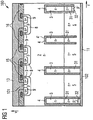
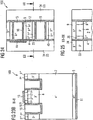
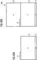
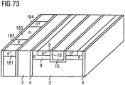
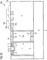
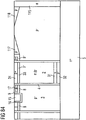
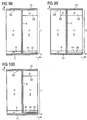
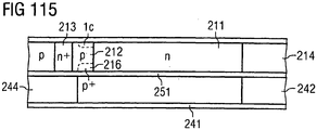
- FIG. 1 shows a cross section through a portion of an embodiment of a power semiconductor device.
- the illustrated device is designed as a planar MOSFET and has a drift zone 2, a source zone 9, and a body zone 8, which is arranged in a complementary manner to the source zone 9 and is arranged between the source zone 9 and the drift zone 2.
- a gate electrode 15 which is insulated from the semiconductor body by a gate dielectric 16.
- the gate electrode is arranged above a front side 101 of the semiconductor body 100 and extends in a lateral direction r of the semiconductor body 100 from the source zone 9 to the drift zone 2, which reaches the front side 101 in sections.
- the device further comprises a drain zone 5, which adjoins the Drift zone 2 connects, which is doped higher than the drift zone and which is contacted by a drain electrode 11.
- the drain zone 5 of the illustrated device can be realized, for example, by a semiconductor substrate, to which an epitaxial layer with a basic doping is applied. Portions of the epitaxial layer that have the basic doping form the drift zone 2. It should be noted that the dimensions of the semiconductor substrate and the epitaxial layer in FIG. 1 are not reproduced to scale.
- the illustrated MOSFET is n-type, the source region 9, the drift zone 2 and the drain zone 5 are n-doped, while the body zone is p-doped.
- the invention is of course also applicable to a p-type MOSFET, whose device zones are doped complementary to those of an n-type MOSFET.
- MOSFET is realized as a vertical MOSFET.
- the source zone 9, the body zone 8, the drift zone 2 and the drain zone 5 of this component are arranged successively in a vertical direction v of the semiconductor body 100.
- a conductively driven component ie when a positive voltage is applied between drain and source and a suitable drive potential is applied to the gate electrode 15, a current flows in the vertical direction through the drift zone between source and drain.
- the body zone 8 and the drain zone 5 form in this component first and second component zones between which the drift zone 2 is arranged, wherein, when a reverse voltage is applied between the body zone 8 and the drain zone 5, a space charge zone in the drift zone 2 starts from the semiconductor junction between the body zone 8 and the drift zone 2 propagates.
- the drift control zones 3 are coupled to one of the load terminal potentials of the MOSFET, which abut the drain 5 and / or source 9 during operation.
- the drift control zones 3 are connected to the drain zone 5 for this purpose.
- the connection of the drift control zones 3 to this drain zone 5 can take place in different ways. In FIG. 1 For this purpose, four different options are shown.
- the drift control zone 3 can be connected to the drain electrode 11 via a heavily doped first connection zone 31 of the same conductivity type as the drift control zone.
- the dielectric layer 4 extends as far as the drain electrode 11 and thereby dielectrically isolates the first connection zone 31 and the drain zone 5 from one another.
- a second connection zone 32 doped complementary to the first connection zone and doped weaker than the first connection zone 31 may be arranged between the highly doped first connection zone 31 and the drain electrode 11.
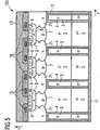
- the device according to FIG. 1 is cell-like and has a number of similar transistor cells, each having a source and a body zone 9, 8.
- the individual transistor cells are connected in parallel by connecting their source zones 9 to a common source electrode 13 and by connecting their gate electrodes 15 to a common gate terminal (not shown).
- the drift zone 2 is common to all transistor cells in the illustrated device.
- the drain zone 5 can be realized as a continuous semiconductor region common to all the transistor cells, or have a plurality of separate semiconductor sections which are connected to one another by the drain electrode 11.
- the drift control zone 3 can in particular be doped so that it can be cleared not only in sections but completely in a direction perpendicular or transversely to the direction of current flow.
- the quotient of the net dopant charge present in the drift control zone and the surface of the accumulation dielectric 4 extending in the current flow direction between the drift zone 2 and the drift control zone 3 is then smaller than the breakdown charge of the semiconductor material used for the drift control zone 3.
- drift control zones which are bounded by the dielectric layer 4 to two sides and upwards.
- the special case is also assumed below that the drift control zones 3 are each doped homogeneously.
- the aforementioned doping rule is equivalent to the fact that the integral of the ionized dopant concentration of the drift control zone 3 in a direction r perpendicular to the accumulation dielectric 4 and over the entire "width" of the drift control zone 3 is smaller than twice the breakdown charge of the semiconductor material the drift control zone 3.
- this breakdown charge is about 1.2 ⁇ 10 12 e / cm 2 , where e denotes the elementary charge.
- drift control zone Considering a homogeneous doped drift control zone, not shown, to which only on one side of a drift zone connected to the drift control zone by a dielectric layer, it is true for this drift control zone that the integral of the dopant concentration in the direction perpendicular to the dielectric layer is smaller than the breakdown charge. Such a drift control zone is then completely erasable by an electric field which is applied via the accumulation dielectric 4.
- the accumulation dielectric 4 can completely separate the drift control zone 3 from the drift zone 2 and thus form a completely closed area between the drift control zone 3 and the drift zone 2.
- the dielectric layer forming the accumulation dielectric 4 in sections as a so-called tunnel dielectric, in particular as tunnel oxide. This is in FIG. 1 for one of the drift control zones 3, in which the dielectric is formed above the drift control zone 3 as a tunnel dielectric 4 '. The function of this tunnel dielectric will be explained below.
- the drift control zone 3 preferably has the same doping profile in the current flow direction, ie in the vertical direction v, as the section of the drift zone 2 arranged transversely to the current flow direction adjacent to the drift control zone 3, which extends over the same region in the current flow direction (vertical direction v) as the drift control zone 3 extends.
- the drift control zones 3 are adapted to the grid of the cell array arranged in the region of the front side 101, wherein the drift control zones 3 are respectively arranged between two adjacent body zones 8 in the lateral direction of the semiconductor body 1.
- the drift control zones 3 can also be arranged under the body zones 8 (not shown).
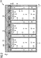
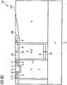
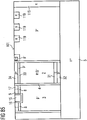
- FIG. 2 Another embodiment of a designed as a MOSFET device FIG. 2 , This component differs from the device according to FIG. 1 in that the drift control zones 3 extend as far as the front side 101 of the semiconductor body 1.
- the drift control zones 3 in the example in the area of the front side are also covered by the dielectric layer 4 forming the accumulation dielectric 4 or the tunnel dielectric 4 '.
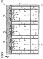
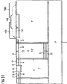
- FIG. 3 shows a further embodiment in which the dielectric layer forming the accumulation dielectric 4 is adjacent to the drift control zone 3 only in a lateral direction.
- a dielectric or an insulator is applied, which covers the drift control zone.
- the drift control zone 3 is covered by the gate dielectric 16.
- the drift control zone 3 of each cell is thereby electrically insulated in the region of the front side of the semiconductor body 1 (source side) from the gate electrodes 15 and the source electrode 13.
- the components of the Figures 2 and 3 in which the drift control zones 3 extend to the front side of the semiconductor body it is also possible to connect the drift control zone 3 to the source electrode 13 via a connection zone 35 doped complementary to the drift control zone 3 and a tunnel dielectric 4 ', as shown for the drift control zone 3 , in the FIG. 2 shown on the far right.
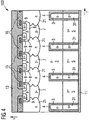
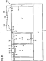
- the drift control zones 3 are respectively arranged between the intermediate zones 21 and the drain electrode 11.
- the drift control zones 3 surrounded by the dielectric 4 in the semiconductor body terminate in the vertical direction at a distance from the intermediate zones 21.
- the drift control zones 3 with the surrounding dielectric 4 can also extend as far as the intermediate zones 21 or extend into the intermediate zones 21.
- the drift control zones 3 can also extend as far as the front side of the semiconductor body (not shown).
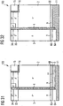
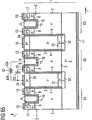
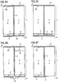
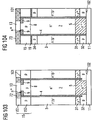
- FIG. 6 Another embodiment of a MOSFET with drift control zones 3 shows FIG. 6 , Here, a plurality of drift control zones 3, which are coupled to the drain zone, are arranged unevenly in the semiconductor body 100 in the lateral direction. The distance between adjacent drift control zones 3 in the area of the compensation zones 7 is chosen to be smaller than in other areas.
- the drift control regions 3 may be equidistant from each other in the lateral direction of the semiconductor body 1.
- FIGS. 1 to 7 show MOSFETs with planar gate electrodes.
- the concept of the present invention to provide a drift control zone 3 consisting of a semiconductor material which is insulated from a drift zone 2 by an accumulation dielectric 4 and whose net dopant charge related to the surface of the dielectric 4 is smaller than the breakdown charge, can of course also apply Trench MOSFETs with a vertical in a trench arranged gate electrode 15 are applied.
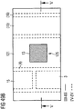
- FIG. 8 shows such a trench MOSFET with several drift control zones 3.
- the source zone 9 the body zone 8 doped to the source zone, the drift zone 2 and the heavily n-doped junction zone or drain zone 5 arranged in direct succession.
- the trench MOSFET has electrically conductive gate electrodes 15, which are made of, for example, a metal or a highly doped polycrystalline semiconductor material, for.
- Example, polysilicon which are electrically insulated by means of a gate dielectric 16, for example a semiconductor oxide, with respect to the other regions of the semiconductor body 100 and with respect to the source electrode 13.
- the gate electrode 15 is arranged in trenches which extend through the source zones 9 and body zones 8 to 13 into the drift zone.
- the drift control zone 3 is connected to the drain electrode 11 and thus to the drain zone 5, as in the preceding exemplary embodiments, by means of a heavily n-doped first connection zone 31.
- the drift control zones 3 may extend over the same area as the drift zone 2 in the vertical direction v.
- the third connection zone 33 extends in the vertical direction v over the same area as the body zone 8, the fourth connection zones 34 over the same vertical area as the source zone and the first terminal zone 31 over the same vertical area as the drain zone 5.
- the drift control zone 3 is connected by means of the heavily n-doped first Verbin Printergszone 31 to the drain electrode 11 and thus to the drain zone 5.
- the various, based on FIG. 1 explained ways to electrically connect the drift control zone 3 to the drain zone 5, also on the device according to FIG. 10 , to the components of the previously explained FIGS. 2 to 9 and to the below-explained device according to FIG. 11 are applicable.
- a heavily p-doped semiconductor zone 17 Adjacent to the dielectric layer forming the accumulation dielectric 4, a heavily p-doped semiconductor zone 17 can be arranged in the body zone 9 and in sections in the source zone 8, as is the case for one of the transistor cells in the right-hand part of FIG. 10 is shown.
- This zone 17 which is referred to below as a bypass zone, forms a very low-impedance bypass for holes to the source electrode 13 and thus prevents an early latency of the cell, in particular in the operating cases "avalanche" and "commutation" of the power semiconductor component.
- This zone 17 also prevents a controllable by the drift control zone 3 channel between the source zone 9 and the drift zone 2 is present.
- this semiconductor zone 17 effects a low-resistance connection of the source electrode 13 to the body zone 8.
- this zone 17 effects a low-resistance connection of the source electrode 13 to the body zone 8.
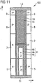
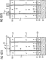
- FIG. 11 shows a possibility to reduce the sensitivity of the semiconductor body 1 with respect to mechanical stresses which can be produced by producing the drift control zones 3 with the accumulation dielectric 4 surrounding them.
- the dielectric 4 is made of dielectric partial layers 4a, 4b, between which there is a gap 4c which is filled with a compressible medium such as a gas, for example air.
- the sublayers 4a, 4b of the dielectric 4 may rest on the source side or may be integrally formed thereon. Furthermore, webs may be provided for stabilization between the sub-layers 4a, 4b, which may consist of the same material as the sub-layers 4a, 4b.
- the drift control zone 3 is thereby at a higher potential than the drift zone 2, wherein this potential difference increases with increasing distance from the drain zone 5 in the direction of the body zone 8.
- This potential difference causes an accumulation zone to form in the drift zone 2 adjacent to the accumulation dielectric 4, in which charge carriers, in the present case electrons, are accumulated.
- This accumulation zone causes a reduction of the on-resistance of the device compared to conventional devices.
- a space charge zone is also built up in the vertical direction in the blocking case, which results from the fact that the voltage drop across the accumulation dielectric 4 is limited to an upper maximum value due to the low doping of the drift control zone 3.
- the accumulation dielectric 4, together with the drift control zone 3 and drift zone 2, forms a capacitor for whose capacitance coating C 'the following applies: C ' ⁇ 0 ⁇ ⁇ r / d battery pack ⁇ 0 denotes the dielectric constant for the vacuum and ⁇ r denotes the relative dielectric constant of the dielectric used, which is about 4 for silicon dioxide (SiO 2 ).
- a space charge zone builds up in the drift control zone 3, the potential curve of which can differ from the potential curve of the drift zone 2 by the value of the voltage applied across the dielectric 4 and limited by the low doping of the drift control zone 3.
- the voltage across the accumulation dielectric 4 is always lower than its breakdown voltage.
- the semiconductor components explained so far and those explained below are n-conducting components, the majority charge carriers flowing in the drift zone 2 when the component is driven in a conductive manner are electrons in this case.
- the inventive concept is not limited to n-type components, but also applicable to p-type devices, wherein the semiconductor regions of a p-type device to be doped complementary to the semiconductor regions of the previously explained n-type devices.
- the drift control zones 3 are connected exclusively to the drain zone 5.
- holes can be accumulated in the drift control zones 3 which arise as a result of thermal generation of electron-hole pairs and which can not flow away. Over time, this amount of charge can increase so much that the maximum permissible field strength of the accumulation dielectric 4 is reached and the dielectric 4 breaks through.
- the accumulation dielectric forming dielectric layer 4 is partially formed as a tunnel dielectric 4 '. This tunnel dielectric allows the accumulated charge carriers to drain into the drift zone 2 as soon as the breakdown field strength of the tunnel dielectric 4 'is reached and even before the breakdown field strength of the accumulation dielectric 4 is reached.
- Suitable tunnel dielectrics are, for example, layers of silicon oxide (SiO 2 ) or silicon nitride (Si 3 N 4 ) or else multilayer layers of silicon oxide and silicon nitride. Also possible are mixed dielectrics made of silicon, oxygen and nitrogen. Typical tunnel field strengths are in the range of 1 ... 2V / nm. For a tunnel oxide 4 'with a thickness of 13 nm, this results in maximum voltages of 13... 26 V, which is above the voltage applied to the dielectric 4 during the normal blocking operation and that of a dielectric 4 made of silicon oxide with a thickness of, for example, 100 nm easily endured.
- the tunnel dielectric is arranged at the upper end of the drift control zone 3. It is particularly advantageous that the accumulated holes support the switching on of the component because they support the generation of an accumulation zone in the drift zone 2 until the difference between the potential of the drift zone 2 and the drain zone 5 has dropped below the value of the tunneling voltage. After that, excess holes flow out of the drift control zone 3 in the direction of the drain zone 5 or drain electrode 11.
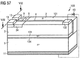
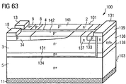
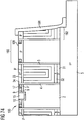
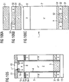
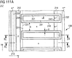
- FIG. 12 shows a detail of another embodiment of a device which is formed as an n-type trench MOSFET. Shown in side view in cross section one of a plurality of identical transistor cells of the device.
- the component has a component structure of a conventional vertical trench MOSFET 20 with a source zone 9, a body zone 8, a drift zone 2 and a drain zone 5 and a gate electrode 15 arranged in a trench.
- the source zone 9 is contacted by a source electrode 13 and the drain zone 5 is contacted by a drain electrode 11.
- the p-doped body zone 8 is connected via the heavily p-doped bypass zone 17 to the source electrode 13, which forms a very low-impedance bypass for holes to the source zone 9 and thus an early latency of the cell, especially in the operating cases “avalanche” and Prevents “commutation” of the power semiconductor device.
- This zone 17 also prevents a controllable by the drift control zone 3 channel between the source zone 9 and the drift zone 2 is present.
- a drift control zone 3 Adjacent to the drift zone 2, a drift control zone 3 is arranged, which is connected by means of a heavily n-doped first connection zone 31 to the rear-side drain electrode 11.
- the drift control zone 3 extends in this component in the vertical direction approximately to the front of the semiconductor body 1 and is thus arranged in sections adjacent to the body zone 8.
- a heavily n-doped further connection zone 133 which contacts a fourth electrode 19 arranged on the semiconductor body 1, adjoins the drift control zone 3. This fourth electrode 19 is separated from the source electrode 13 in the example.
- the drift control zone 3 forms, together with the first connection zone 31 and the further connection zone 133, a junction field-effect transistor (JFET) whose gate represents the body zone 8 or bypass zone 17.
- JFET junction field-effect transistor
- This junction field-effect transistor 31, 3, 33 can be switched off by a sufficiently high negative potential of the body zone 8.
- dielectric 4 present here does not hinder the pinch-off effect.
- the drift control zone 3 is connected via a first diode 41 to the source zone 9 or source electrode 13 connected.
- An anode 41a of this diode 41 is electrically conductively connected via the source electrode 13 to the source zone 9 and a cathode 41b via the fourth electrode 19 to the drift control zone 3 and the junction field effect transistor 31, 3, 133, respectively.
- the diode 41 no high demands are to be made with regard to the leakage current. Since the junction field effect transistor 31, 3, 133 in the off state of the MOSFET is turned off and no current can flow from it, it is irrelevant if the first diode 41 has a high leakage current.
- FIG. 12 shows only a section or a cell of the entire component. On the left side, this section is followed by another section of the dielectric 4 followed by another trench MOSFET structure (not shown).
- the illustrated MOSFET structure and the further MOSFET structure are mirror-symmetrical to one another in the vertical direction v and perpendicularly extending through the plane of representation symmetry plane.
- Locking the device by the gate electrode 15 is suitably controlled, so in the drift zone 2, starting from the pn junction, a space charge zone spreads, and the voltage across the drift path 2 increases.
- the potential of the drift control zone 3 initially follows the potential of the drain zone 5 or drain electrode 11.
- the barrier layer FET formed by the drift control zone 3 the dielectric 4 and the body zone 4 is increasingly pinched off until it completely locks and holds the potential in that region adjacent to the body zone at a value different from the potential of the body zone 8 by the value of the blocking voltage of the blocking FET.
- the barrier FET formed in the upper region of the drift control zone protects the diode 41 from excessively high voltages as the drain potential increases further.
- the voltage for the complete pinch-off of the junction FET is set so that it is less than the breakdown voltage of the diode 41st
- the voltage drop across the drift control zone 3 decreases in the lower region, ie in the region between the heavily doped connection zone 31 and the body zone 8, corresponding to the voltage drop across the drain Drift zone 2, whereby in the drift control zone 3 with increasing voltage, a space charge zone further propagates in the direction of the heavily doped connection zone 31.
- This space charge zone propagating in the drift control zone 3 and the space charge zone propagating in the drift zone 2 limit a maximum voltage present between the drift control zone 3 and the drift zone 2 via the accumulation dielectric 4.
- this voltage is approximately in the range of the turn-off voltage of the junction FET and is usually a few volts, so that the accumulation dielectric 4 is not subject to high voltage stress and are dimensioned correspondingly thin can.
- a thin dielectric 4 is again advantageous with respect to the accumulation of charge carriers in the drift zone 2 in the case of a conductively driven component, the better the accumulation behavior the thinner the dielectric 4 is at a given potential difference between drift control zone 3 and drift zone 2.
- the advantage of the arrangement according to FIG. 12 consists in that via the diode 41, a current path between the terminal electrodes and drain and source electrodes 11, 13 of the device is present, via which thermally in the drift control zone 3 generated charge carriers can flow, so that it is not in the blocking case to the previously described undesirable Accumulation of charge carriers in the drift control zone 3 or on the dielectric 4 comes.
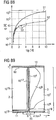
- FIGS. 13 and 14 are the electron distribution of a conventional MOSFET and the MOSFET according to FIG. 12 in a conducting state, each with a gate voltage of 10 V and each with a drain-source voltage of also 10 V compared.
- FIG. 13 shows the electron distribution of the conventional MOSFET
- FIG. 14 the electron distribution of the MOSFET FIG. 12 .
- FIG. 15 shows a characteristic curve 59, the course of the drain-source current I DS of a MOSFET according to the prior art in comparison to the corresponding characteristic curve 58 of a MOSFET according to the invention according to FIG. 12 as a function of the drain-source voltage U Ds .
- the load current I DS of the MOSFET according to the invention at a drain-source voltage of 4 V by a factor of 4, at a drain-source voltage of 10 V by a factor of 7 above the drain-source current I.
- DS of a MOSFET according to the prior art although the available for the current flow cross section is significantly reduced in the inventive MOSFET due to the required space for the drift control zone over the cross-sectional area of a MOSFET according to the prior art.
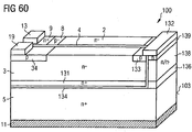
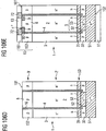
- FIG. 16 shows a trench MOSFET, which differs from the MOSFET according to FIG. 12 differs in that the drift control zone 3 via a weakly p-doped third connection zone 33 and a heavily p-doped fourth connection zone 34 with the fourth electrode 19 is electrically connected.
- the two-stage embodiment of the p-doped connection zone with a more heavily doped zone 34 and a weaker doped zone 33 is optional.
- the task of the higher-doped zone 34 is essentially to achieve a low-resistance connection of the connection electrode 19 to the weaker p-doped zone 33, which forms a pn junction with the drift control zone 3.
- the MOSFET is in the blocking state, in which a voltage of a few 10 V or even a few 100 V is applied between the drain and the source electrode 11, 13 or over the drift path 2 of the MOSFET structure, and that the source electrode 13 is at a reference potential, eg 0V.
- the potential at the fourth electrode 19 is then at most approximately the value of the breakdown voltage of the first diode 41, for example +15 V, above this reference potential.
- the remaining part of the reverse voltage, ie the difference between the drain potential and this potential at the fourth electrode 19, is essentially absorbed by the low-doped drift control zone 3, in which, starting from the pn junction between the drift control zone and the p-doped Zones 33, 34 forms a space charge zone.
- the space charge zones propagating in the drift zone 2 and in the drift control zone 3 in this case limit the voltage applied in the blocking case via the accumulation dielectric 4, since no accumulation or inversion layers can form on the accumulation dielectric 4 in the area of the space charge zones.
- this voltage corresponds to the maximum blocking voltage the diode 41.
- This diode 41 ensures that the p-zone 33 is in the blocking case in comparison to the body zone at a higher potential.
- the doping of the drift zone 2 and the drift control zone 3 can be different, in which case the voltage load of the accumulation dielectric can be greater in comparison to the same doping of the two zones.
- the doping of the drift control zone 3 should be matched to the doping conditions in the drift zone 2, the dielectric strength of the accumulation dielectric 4 and the desired dielectric strength of the component such that no avalanche breakdown occurs in the drift control zone 3 at a maximum permissible reverse voltage and a space charge zone occurs the drift control zone 3 propagates so far in the current flow direction that the electric field formed from the field strength components in the current flow direction and perpendicular to the current flow direction does not exceed the breakdown field strength of the semiconductor material.
- the diode 41 is optionally present in this device. This diode 41 supports a charge storage in the drift control zone 3 with the blocking element, so that less charge has to be re-supplied with conductive activation.
- the region of the drift zone 2 arranged close to the body zone 8 rapidly drops to potentials below the breakdown voltage of the first diode 41. This will cause holes from the top, i. withdrawn near the fourth electrode 19 located area of the drift control zone 3 and in lower, i. shifted in the direction of the drain electrode 11, areas. There, the holes on the opposite side of the dielectric 4, i. on the drift control zone 3 facing side of the drift zone 2, an accumulation of electrons. The charge shifts from the storage capacity into a lower "accumulation capacity".
- the drift zone 2 can be considered as a control electrode for a hole channel at the drift zone 2 side facing the highly n-doped junction zone 31. This hole channel must be absolutely prevented in order to maintain the necessary hole accumulation in the drift control zone 3.
- connection zone 31 in the lateral direction in the region particularly high, which adjoins directly to the dielectric 4 in order to avoid the formation of a hole channel; in the other regions of the connection zone 31, a lower doping can be selected. It may be sufficient, the doping of the connection zone 31 in the area subsequent to the dielectric 4 in the vertical direction not over the entire width of the connection zone 31 but only in sections to increase.
- thermally generated electrons can flow out of the drift control zone 3 via the arrangement with the first and second connection zones 31, 32.
- the holes required by the conductive component in the drift control zone 3 are thus displaced only between the lower n-doped "accumulation region" (opposite the drift zone 2) and the upper p-doped "memory region" 33, 34, so that only a charge shift takes place here the holes do not have to be fed from the drain-source current of the device at each turn-on.
- the switching losses of the device are thereby minimized.
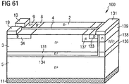
- FIG. 16 illustrated storage capacity does not necessarily have to be completely part of the semiconductor body 1.
- a further capacitance may also be present, which may also be arranged outside the semiconductor body.
- Capacitor is shown and is hereinafter referred to as external capacitance, which can be realized in any way inside or outside the semiconductor body.
- This further capacitance 50 is connected between the source electrode 13 and the fourth electrode 34, and thus between the drift control zone 3 and the source zone 9.
- connection zones 33, 34 doped complementary to the drift control zone 3 are arranged, which form an internal storage capacity.
- This p-doped memory area 33, 34 may, in providing the external capacitance 50 according to the device according to FIG. 12 be replaced by a heavily n-doped junction zone 33 (not shown).
- An advantage of the p-doped connection zones 33, 34 is their more favorable leakage current behavior.
- the memory capacity be it an internal capacity as in FIG. 16 or an internal and external capacity as in Figure 17A , is charged when the device is switched on and that the charges that are lost due to leakage currents are re-supplied.
- a second diode 42 is provided, which is connected between the gate electrode 15 and the drift control zone 3.
- an anode 42a of the diode 42 is connected to the gate electrode 15, and a cathode 42b is connected to the fourth electrode 19 and to the terminal of the external capacitance facing away from the source electrode 13.
- the p-doped zone 34 should have a sufficiently high doping above the drift control zone.
- An external capacitor 50 and a second diode 42 can also be used in the device according to FIG. 12 be provided, as shown in dashed lines there.
- the memory capacity of the components of the Figures 12 and 17A, 17B is formed by an internal and / or external capacitance, charged via the second diode 42 from the gate circuit, if it has not already been charged by the thermal reverse current from the drift control zone 3.
- lost holes are immediately re-supplied from the gate circuit.
- the dynamic transhipment of storage and accumulation capacity while the external control terminals, ie the gate electrode 15, in the steady state no or only very little power withdrawn.
- a pn junction between the Drift deviszone 3 and the drain electrode 11 may be provided, which in the device according to Figure 17A is formed by the n-doped first connection zone 31 following the drift control zone 3 and a weaker p-doped second connection zone 32, which adjoins the drain electrode 11.
- the diode formed by the first and second connection zones 31, 32 should have a reverse voltage higher than a maximum allowable gate voltage applied to conductively drive the device between the gate and source.
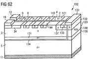
- Figure 17B shows one opposite Figure 17A modified component in which the drift control zone 3 via an optional highly doped first connection zone 31, the doping of which doping may correspond to the drain zone 5, and a tunnel dielectric 4 'is connected to the drain electrode 11.
- the tunnel dielectric 4 ' prevents in the case of passage that accumulated holes in the drift control zone 3 can drain to the drain electrode 11 and allows in the case of blocking the outflow of a thermally generated leakage current to the drain electrode 11.
- the dielectric strength of the tunnel dielectric 4' only has to be so high that it can lock the gate voltage.
- the tunnel dielectric 4 'monocrystalline semiconductor material is located above the tunnel dielectric 4 'monocrystalline semiconductor material.
- Such a device may be manufactured by epitaxially growing the semiconductor material on the tunnel dielectric.
- the drain zone 5 represents the substrate onto which the tunnel oxide is applied, on which the epitaxial layer is then grown.
- the tunnel dielectric 4 ' between the drift control zone 3 and the high-n doped drain zone 5 (not shown).
- FIG. 18 shows a further possibility of how a discharge of the (hole) storage capacity in the direction of the drain zone 5 can be prevented.
- the drift control zone 3 is connected via a highly doped connection zone to a second electrode 12 which is separate from the drain electrode 11.
- a third diode 43 is connected, which can also be realized as an external component and whose anode 43a is connected to the drain electrode 11 and the cathode 43b to the second electrode 12.
- the blocking capability of the third diode 43 should be higher than the maximum gate voltage for turning on the MOSFET and may be lower than the allowable potential difference across the accumulation dielectric 4.
- the drift control zone 3 When the MOSFET is first turned on, the drift control zone 3 is charged from the gate circuit to a maximum gate voltage, for example, 10V. Turning off the MOSFET shifts the charge from the accumulation capacity to storage capacity.
- the storage capacity should be chosen so large that the reverse voltage of the second diode 42, for example, 15 V, is not exceeded.
- the storage capacity is preferably 2 to 3 times the accumulation capacity between the drift control zone 3 and the drift zone 2 and consists of the sum of the internal capacity formed by the connection zones 33, 34 and the bypass zone 17 and the optional external accumulation capacity 50.
- such a capacitance can also be integrated into the component, for example into the semiconductor body 1.
- the storage capacity can be increased towards the bypass zone 17 through a dielectric 4 having a higher dielectric constant and / or by enlarging the interface between the hole bypass 17 and the dielectric 4 (not shown).
- drift control zone 3 complementary to the drift zone 2, in the example according to FIG. 18 So to provide a p-doped drift control zone 3.
- These space charge zones propagating from different directions cause a voltage drop across the accumulation dielectric, which causes space charge zones in this component also to propagate laterally in the drift zone 2 and the drift control zone 3.
- this results in a compensation effect that allows a higher basic doping of the drift zone 2 with the same dielectric strength.
- the doping of the drift zone 2 and the drift control zone 3 with the same doping type is for example in the range of 10 14 cm -3 , while in a complementary doping of drift zone 2 and drift control zone 3 doping in the range of 10 15 cm -3 to 10 16 cm -3 possible are.
- FIG. 19 shows a further possibility for connecting the drift control zone 3 to the drain zone 5.
- the drift control zone 3 is connected via the complementarily doped connection zones 31, 32 directly and without interposition of the drain electrode 11 with the drain zone 5. This is achieved in that the dielectric layer forming the accumulation dielectric 4 starts at a distance from the drain electrode 5 and that the drain zone 5 extends in a lateral direction as far as below the drift control zone 3.
- a plurality of individual cells in the present case a plurality of MOSFET cells, can be arranged in the same semiconductor body and connected in parallel with one another.
- two adjacent cells of the component can use an intermediate, common drift control zone 3.
- a capacitance connected to the source zone 9 is either in FIG. 19 shown as an external device capacitance 50 or an internal capacitance formed by the heavily doped junction zone 34, the heavily doped junction zone 17 of the body zone 8 and the intervening dielectric.
- a center tap of the capacitive voltage divider formed by these two capacitances forms the connection electrode 19 of the drift control zone 3.
- a signal which is related to the load path voltage of the power semiconductor component can thus be tapped directly.
- FIG. 20 shows a modification of the in FIG. 19 illustrated vertical power device.
- a higher than the drift zone 2 doped intermediate zone 22 of the same conductivity type as the drift zone 2 is present between the body zone 8 and the drift zone 2.
- This intermediate zone 22 extends in the lateral direction r of the semiconductor body 100 from the gate dielectric 16 to the accumulation dielectric 4.
- the object of this intermediate zone 22 is, in the case of a conductively driven component, the transverse conductivity between the inversion channel which forms in the body zone 8 along the gate dielectric 16 , and to increase the accumulation channel, which forms along the accumulation dielectric 4 in the drift zone 2, or to reduce the electrical resistance between the lateral direction of the semiconductor body r spaced from the accumulation channel arranged inversion channel.
- the path of the charge carriers through the device between the source zone 9 and the drain zone 5 is in FIG. 20 illustrated by dashed lines.
- the doping concentration of this intermediate zone 22 is, for example, in the range between 10 15 cm -3 and 10 17 cm -3, and thus one to two orders of magnitude above the doping concentration of the drift zone second
- the higher doped intermediate zone 22 increases at a constant doping concentration of the drift zone 2, the number of dopant atoms between the body zone 8 and the drain zone 5, which basically leads to a reduction in the dielectric strength of the device.
- the doping concentration of the drift zone 2 can be reduced by providing a more highly doped intermediate zone 22.
- FIG. 21 a Field electrode 23 may be provided, which is disposed adjacent to the higher doped intermediate layer 22 and which is dielectrically insulated by a dielectric layer 24 with respect to the intermediate zone 22 and the drift zone 2.
- the field electrode 23 is arranged in the illustrated embodiment in the vertical direction v of the semiconductor body 100 immediately adjacent to the gate electrode 15.
- the field electrode 23 is for example electrically connected to the source electrode 13 and is thus at source potential of the semiconductor device.
- the task of this field electrode 23 is to compensate at least a portion of the dopant charge present in the intermediate zone 22 when the semiconductor component is driven in the off state, that is to say when a space charge zone is formed starting from the pn junction between the body zone 8 and the higher doped intermediate zone 22.
- the intermediate zone 22 can thereby be doped higher with respect to a component without field electrode 23 with the same dielectric strength of the component.
- the drift control zone 3 is connected via the already explained connection zones 31, 32 to the drain zone 5 and also the connection zones 33, 34 already explained to the connection electrodes 19. It should be noted that the drift control zone course also according to the comments on the Figures 12 . 17 and 18 may be connected to the drain zone 5 and the connection electrode 19.
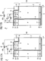
- FIG. 22 shows a cross section through the in the FIGS. 20 and 21
- the gate electrode 15 runs in the lateral direction of the semiconductor body 100 essentially parallel to the drift control zone 3 FIGS. 20 and 21
- the higher doped intermediate zones 22 increase the transverse conductivity between the inversion channel along the gate electrode 15 and the accumulation channel along the accumulation dielectric 4.
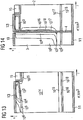
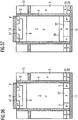
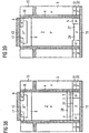
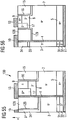
- Figure 23A shows in one of the sectional plane II corresponding sectional plane opposite to the components of FIGS. 20 and 21 modified component.
- a cross section through this device in an in Figure 23A shown section plane II-II is in FIG. 23B shown.
- the sectional view in Figure 23A shows the highly doped connection zones 17 and the source zones 9, the body zones 8 are arranged below these connection zones 17 and the source zones 9.
- the gate electrodes 15 are insulated from the body zones by the gate dielectric 16 and also insulated from the drift control zone 3 by means of a dielectric layer.
- the gate dielectric 16, the accumulation dielectric 4 and the dielectric 25 insulating the gate electrode 15 with respect to the drift control zone 3 can in this case consist of the same material or a material with the same dielectric properties.
- FIGS 23A and 23B illustrated component extend a surface of the gate dielectric 16, along which the inversion channel in the body zone 8 is formed at leited driven device, and a surface of the accumulation dielectric 4, along which the accumulation channel in the drift zone 2 forms, perpendicular to each other.
- the inversion channel forming in the upper region of the semiconductor body along the gate dielectric 16 extends in this component in a lateral direction as far as the accumulation channel forming in the lower region of the semiconductor body 100 along the accumulation dielectric 4.
- the source zones 9 are arranged such that they extend in the lateral direction of the semiconductor body 100 do not extend to the accumulation dielectric 4, which in Figure 23A is shown. If, for reasons of process technology, the source zones 9 should extend as far as the accumulation dielectric 4 in the lateral direction of the semiconductor body, different types exist FIG. 24 shown ways to prevent the formation of a no longer disconnectable channel.
- One possibility is to realize the accumulation dielectric 4 thicker in the regions in which the source zone 9 extends as far as the accumulation dielectric 4 than in other regions. This is in FIG. 24 by the provision of an additional dielectric layer 44 immediately following the accumulation dielectric 4.
- the accumulation dielectric 4 in such a way that its dielectric constant is lower in the regions in which the source zone 9 extends as far as the accumulation dielectric 4 than in other regions, in particular in those regions in which the accumulation dielectric is present 4 is to form an accumulation channel in the drift zone 2 in the case of a conductive component.
- This channel stop zone 26 is doped complementary to the source zone 9 and higher than the body zone 8 and serves to prevent a channel controlled by the drift control zone along the accumulation dielectric 4 between the source zone 9 and the drift zone 2.
- a cross section in a sectional plane III-III in the region of this channel stop zone 26 is in FIG. 25 shown.
- the gate electrode 15 is arranged in such extension of the drift control zone 3, that at regardedd controlled Component forms an along the gate dielectric 16 forming inversion channel directly into an accumulating along the Akkumulationsdielektrikum 4 accumulation channel.
- the gate electrode 15 is arranged in the vertical direction of the semiconductor body 100 above the drift control zone 3.
- a common dielectric layer may be provided which forms the gate dielectric 16 in the region between the gate electrode 15 and the body zone 8 and the accumulation dielectric 4 in the region between the drift control zone 3 and the drift zone.
- the gate electrode 15 and the drift control zone 3 are dielectrically insulated from one another by a dielectric, which with regard to its dielectric properties can correspond to the gate dielectric 16 and / or the accumulation dielectric 4.
- the drift control zone 3 can according to one of the previously with reference to the Figures 12 and 17 to 19 explained options to the source electrode 13 or the gate electrode 15 may be coupled.
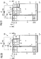
- the illustration of such electrical connections and optionally additionally required components, such as diodes or capacitors, is omitted in FIGS. 26 and 27 for reasons of clarity.
- the gate electrode 15 completely overlaps the region above the drift control zone 3 in sections, ie, the drift control zone 3 does not extend in sections to the front of the semiconductor body 100.
- sections are present in a manner not shown in which the drift control zone 3 reaches the front side of the semiconductor body 100 is enough to be contacted there. These sections are offset in a direction perpendicular to the plane of the drawing shown in FIG FIG. 26 shown portion of the drift control zone. 3
- the gate electrode 15 is formed narrower in a direction perpendicular to the gate dielectric 16 than in the semiconductor device according to FIG. 26 such that the drift control zone 3 in this component past the gate electrode 15 and insulated by a dielectric layer with respect to the gate electrode 15, reaches as far as the front side 100 of the semiconductor body.
- the intermediate layers or contact layers 33, 34 already explained above can be provided, which in FIG. 27 are shown in dashed lines.
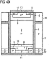
- FIGS. 26 and 27 When the gate electrode 15 is provided in the immediate extension of the drift control zone 3, it can lead to peaks of the electric field propagating in the drift zone 2 at the transition region between the gate electrode 15 and the drift control zone 3 or between the regions in which the inversion channel and the accumulation channel form when the component is turned on in a conductive manner. Such voltage spikes can lead to a premature voltage breakdown in this region of the component. In order to prevent such premature voltage breakdown, reference may be made to FIG. 28 following the body zone 8, a semiconductor zone 81 of the same conductivity type as the body zone 8 is provided. This semiconductor zone 81 is referred to below as the lower body zone or body extension.
- This deeper body zone 81 extends in the vertical direction of the semiconductor body 100 up to the level of the drift control zone 3, but not in the lateral direction of the semiconductor body 100 as far as the accumulation dielectric 4.
- the deeper body zone thereby does not affect the formation of the accumulation channel along the accumulation dielectric 4 in the case of a conductively driven semiconductor component, but in the blocking case shields the electric field from that between the lower body zone 81 and the accumulation dielectric 4 lying area of the drift zone 2 from. This prevents the occurrence of field peaks in this region of the drift zone 2 near the accumulation dielectric 4.
- the lower body zone is relatively low doped, ie, for example, according to the body zone 8 or lower doped.
- the deeper body zone in this case provides a compensation charge to the complementary dopant charge at the upper end of the drift zone 2, ie in the region of the drift zone 2, which is immediately adjacent to the lower lying body zone 81.
- the voltage pickup in the transition region between the lower-lying body zone 81 and the drift zone 2 is thereby increased due to a lower gradient of the electric field, so that field peaks are avoided.
- the deeper-lying body zone 81 in such a way that field-locking peaks in the region of the lower-lying body zone 81 are generated in the case of a blocking component in order to concentrate a voltage breakdown on the lower-lying body zone.
- This can be achieved in that a pn junction between the lower body zone 81 and the drift zone 2 has comparatively strong edges, as for example for the deeper body zone 81 in accordance with FIG FIG. 28 is shown.
- there is the possibility of realizing the deeper body zone 81 such that it extends locally particularly deeply into the drift zone 2, wherein a voltage breakdown then occurs in the regions of the semiconductor body 100 reaching deep into the drift zone 2.
- Such a locally particularly deep course of the deeper body zone 81 is in FIG. 28 shown in dashed lines.
- the deeper body zone 81 is comparatively highly doped, ie, for example, higher than the body zone. 8
- lower-lying body zone 81 can both n-type devices with an n-doped drift zone 2 (as in FIG. 28 shown), as well as in an n-type device with p-doped drift zone, which will be described below with reference to the FIGS. 41 to 43 will be explained.
- the drain zone 5 of the device via a rectifier element, in this case a diode, or a tunnel dielectric to the drift control zone 3 is connected.
- This diode can be referred to the Figures 16 . 17A and 19 be formed by a pn junction between two complementary doped connection zones 31, 32, which are arranged in the direction of the back of the semiconductor body 100 successively following the drift control zone 3.
- Such a pn junction between the drain zone 5 and the drain electrode 11 and the drift control zone 3 can be referred to FIG. 29 be replaced by a Schottky junction.
- a Schottky contact is present between a Schottky metal 64, such as platinum, and an intermediate zone 65 doped higher than the drift control zone 3.
- This intermediate zone 65 is not required for the formation of a Schottky contact, but serves as a stop zone, which prevents a drainage of holes from the drift control zone 3 to the drain electrode 11.
- FIG. 30 shows the device according to FIG. 29 during a possible manufacturing process.
- this method after making the hole stop zone 65 and applying the Schottky metal 64 to this hole stop zone 65, an ion implantation over the exposed backside of the semiconductor body 100 performed.
- n-dopant atoms are implanted into the drift zone 2 via the rear side of the semiconductor body 100.
- the Schottky metal 64 in this case acts as a mask, which prevents implantation of the dopant atoms into the drift control zone 3.
- a semiconductor region of the drift zone 2, in which the n-type dopant atoms are implanted, is in FIG. 30 denoted by the reference numeral 5 '.
- the semiconductor device is completed by applying a backside metallization forming the drain electrode 11 and an annealing step by heating the semiconductor body 100 in the back region to electrically activate the dopant atoms implanted in the semiconductor region 5 'and thereby deliver the heavily doped drain region 5 form, which simultaneously produces a low-resistance electrical contact between the drain electrode 11 and the drift zone 2.
- the activation of the dopant atoms implanted for producing the hole stop zone 65 and / or production of the drain zone 5 can be effected by heating the rear side of the semiconductor body 100 by means of a laser beam (laser annealing).
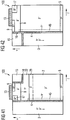
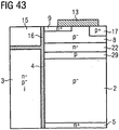
- FIG. 31 shows a variant of in FIG. 29 illustrated semiconductor device.
- the drift zone 2 for example at the same height as the hole stop zone 65, there is a field stop zone 66, which is doped higher than the drift zone 2.
- This field stop zone 66 can be produced, for example, before applying the backside metallization forming the drain electrode 11 by means of an ion implantation and a subsequent annealing process.
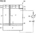
- FIGS. 29 to 32 explained semiconductor structure with the drift control zone 3, the accumulation dielectric 4 and the drift zone 2 as well as with the arranged in the front side of the semiconductor body further device structures can reference to FIG. 33 first on one p-doped semiconductor substrate prepared before forming the Schottky metal (64 in the FIGS. 29 to 32 ) and backside metallization (11 in the FIGS. 29 to 32 ) is to be removed.
- the removal of this p-substrate takes place for example by means of an electrochemical etching process in a basic etching medium, such as NH 4 OH, NaOH, KOH in aqueous solution.
- an electrical voltage is applied by means of a voltage source 68, whereby the p-substrate is electrochemically etched back.
- the current supplied by the voltage source 68 is measured by a current measuring arrangement 69. It makes use of the fact that the flowing current then increases abruptly when the substrate 67 is completely etched back and the etching medium then acts on the n-doped epitaxial layer.
- the flowing current is used in this method as an etching control, wherein the etching process is terminated when the current rises abruptly upon reaching the n-doped epitaxial layer.
- the illustrated method in which the p-type substrate 67 is removed by an electrochemical etching process, is more controllable than a chemical or mechanical ablation process, which method can be combined with such a process by first chemically or mechanically thinning the semiconductor substrate 67 and only then the electrochemical process, which allows an exact end point control is performed.
- FIG. 34 shows a power device, which is improved in terms of its turn-on, turn-off and overcurrent behavior compared to the previously discussed semiconductor devices.
- a complementary to the drift zone doped semiconductor zone 27 is present following the drift zone 2, which is connected together with the drain zone 5 to the drain electrode 11. In the lateral direction, this extends p-zone 27 between the drain zones 5 over the entire width of the drift zone 2 between the accumulation dielectrics 4 of two adjoining the drift zone 2 drift control zones 3.
- the drift control zone 3 is in this device via a formed by the connection zones 31, 32 diode the drain electrode 11 is connected.
- a Schottky diode can also be used to connect the drift control zone 3 to the drain electrode 11.
- FIG. 35 shows a modification of the in FIG. 34 illustrated semiconductor device.
- the p-zone 27 is preceded by a field stop zone 28 of the same conductivity type as the drift zone 2.
- This field stop zone 28, which is doped higher than the drift zone 2 extends in a lateral direction between the two accumulation dielectrics 4 bounding the illustrated drift zone 2 in the lateral direction.
- FIG. 36 Another variant of in FIG. 34 shown semiconductor device is in FIG. 36 shown.
- the dimensions of the p-zone 27 in the vertical direction of the semiconductor body 100 correspond to the dimensions of the drain zone 5.
- the p-zone 27 thus does not extend in the lateral direction of the semiconductor body to the accumulation dielectric 4, so that in the region of the accumulation dielectric 4 the drift zone 2 directly adjoins the drain zone 5.
- FIG. 37 illustrated modification of the FIG. 36 shown component joins the drain zone 5 and the p-zone 27 directly to the field stop zone 28 at.
- this field stop zone 28 may also be spaced from the drain zone 5 and the p-zone 27, as shown in FIG Figure 38 is shown.
- a portion of the drift zone 2 is present between the field stop zone 28 and the drain zone 5 or the p-zone 27.
- FIG. 39 Another variant of in FIG. 36 shown semiconductor device is in FIG. 39 shown.
- the dimensions of the p-zone 27 in the vertical direction compared to the dimensions of the drain zone 5 are smaller, so that the p-zone 27 in the direction of the drain electrode opposite the drain zone 5 is reset.
- FIG. 40 shows the device according to FIG. 39 with additional, the drain zone and the p-zone 27 upstream field stop zone 28th
- FIG. 41 A further exemplary embodiment of a power semiconductor component according to the invention with a drift zone 2, a drift control zone 3 and an accumulation dielectric 4 arranged between the drift zone 2 and the drift control zone 3 is shown in FIG. 41 shown.
- the illustrated device is an n-type MOSFET with an n-doped source zone 9 and an n-doped drain zone 5, but one at least in sections realized p-doped drift zone 2.
- FIG. 41 the connection of the drift control zone 3 to the drain zone 5, the source zone 9 and optionally the gate electrode 15 is not detailed. This connection of the drift control zone 3 to these semiconductor zones can be made using any of the options discussed so far.
- an inversion channel is formed along the accumulation dielectric 4 in the illustrated device in the p-doped drift zone 2.
- the accumulation dielectric 4 thus has the function of an "inversion dielectric" in this component.
- the term “accumulation dielectric” is also used herein for a dielectric along which an inversion channel is formed in a p-doped drift zone 2.
- the gate electrode 15 is arranged in the illustrated component in the lateral direction r of the semiconductor body 100 at a distance from the drift control zone 3.
- a inversion channel forming in the body zone 8 along the gate dielectric 16 in the body zone 8 and the inversion channel forming along the accumulation dielectric 4 in the p-drift zone 2 are thus arranged at a distance from one another in the lateral direction.
- an n-doped intermediate zone 22 is arranged between the body zone 8 and the p-drift zone 2, which increases the transverse conductivity between these two channels, or in the present case enables an electron flow between these two channels.
- Figure 42 shows a modification of the in FIG. 41 illustrated component.
- the gate electrode 15 in the vertical direction v of the semiconductor body above the Drift control zone 3 is arranged.
- the p-drift zone 2 adjoins in this component directly to the p-doped body zone 8.
- the wiring of the drift control zone 3 with the drain zone 5 and the source zone 9 or the gate electrode 15 is not shown in detail. This interconnection can be done in any manner previously explained.
- the doping concentration of the p-drift zone 2 is, for example, in the range of 10 14 cm -3 to 5 ⁇ 10 5 / cm -3 , and thus significantly lower than that of the body zone 8.
- a higher p-doped zone 29 are provided in the in FIG. 41 represented component between the drift zone 2 and the transverse intermediate zone 22 .
- the task of this p-zone 29 is to reduce the electric field strength below the body zone 8 and the gate electrode 15 when the component is driven in a blocking manner.
- a weakly n-doped semiconductor zone 45 can also be provided in the p-drift zone 2 along the accumulation dielectric 4, in which an accumulation channel is formed when the component is driven in a conductive manner.
- the doping concentration of this zone 45 is for example in the range of 10 15 cm -3 to 5 ⁇ 10 16 cm -3 , the width / dimension of this zone in the lateral direction is for example in the range between 0.2 .mu.m - 2 .mu.m.
- This very thin n-doped semiconductor zone 45 has little effect on the blocking behavior of the component, but provides for improved switch-on behavior since a conducting channel for majority charge carriers is always present along the accumulation dielectric 4.
- This n-zone 45 extends in a vertical direction from the n-type intermediate zone 22 to the drain zone 5.
- Such an n-zone can also in the device according to Figure 42 be provided. In this device, the n-zone extends from the body zone 8 to the drain zone 5.
- such a thin and weakly n-doped region 45 may also be dimensioned so that it extends in the vertical direction only from the gate electrode 15 via the gate electrode 15 and the drift control zone 3 separating dielectric up to the level of the drift control zone 3 thereby bridging in the p-drift zone 2 the portion between the inversion channel formed along with the conductive component along the gate dielectric 16 and the accumulation channel propagating along the accumulation dielectric 4.
- FIG. 43 shows a modification of the in Figure 42 illustrated component.
- the p-drift zone 2 is followed by a higher p-doped zone 29, the function of which is to reduce the field strength loading in the upper region of the drift zone 2.
- a weakly n-doped zone 22 is provided, which serves to form the semiconductor region between the gate dielectric 16, along which an inversion channel is formed in the body zone 8 when the component is turned on, and along of the accumulation dielectric 4, along which an accumulation channel is formed in the case of a conductive component, to be "bridged".
- the doping of the p-zone 29 must of course not be so high that the channel along the accumulation dielectric 4 is pinched off.
- the drift control zone 3 does not necessarily have to be n-doped in order to realize an n-type semiconductor device. As explicitly in the FIGS. 41 to 43 Alternatively, the drift control zone 3 may alternatively be weakly p-doped or intrinsic. This applies to all power semiconductor components according to the invention which have been explained above and below.
- FIG. 44 shows another power semiconductor device.
- the illustrated device is realized as a vertical n-type MOSFET.
- the drift control zone 3 is arranged only in sections adjacent to the drift zone 2, ie, does not extend completely along the drift zone 2 in the vertical direction v of the semiconductor body 100.
- the drift control zone 3 is spaced apart from the drain zone 5 in the upper region of the illustrated component
- Semiconductor body 100 is arranged, wherein between the drift control zone 3 and the drain zone 5, a portion of the drift zone 2 is arranged.
- the drift control zone 3 is dielectrically insulated from the drift zone 2 in the illustrated component in the lateral direction r of the semiconductor body by the accumulation dielectric 4.
- the drift control zone 3 can be connected to the source zone 9 and optionally the gate electrode 15 via a heavily doped connection zone 34 as well as diodes and a capacitor (shown in dashed lines) in the manner already explained.
- the device according to FIG. 44 is based on the basic structure of a trench MOSFET, wherein additionally the drift control zone 3 is present along the drift zone 2.
- the gate electrode 15 is arranged in a trench which extends from the front side 101 into the semiconductor body.
- An inversion channel in the body zone 8 is formed in this component in the vertical direction between the source zone 9 arranged in the region of the front side 101 and the drift zone 2 adjoining the body zone 8 in the vertical direction.
- FIG. 45 shows a modification of the in FIG. 44 illustrated component.
- the illustrated device is based on the basic structure of a planar MOSFET.
- the gate electrode 15 is above the Front side 101 of the semiconductor body 100 is arranged and isolated by the gate dielectric 16 with respect to the semiconductor body 100.
- the gate electrode 15 extends as far as the accumulation dielectric 4 extending in the vertical direction v into the semiconductor body 100.
- the gate electrode 15 may end in the lateral direction even before the accumulation dielectric 4 (not shown), but should extend in a lateral direction from the source zone 9 to a section of the drift zone 2 extending to the front side 101.
- An inversion channel is formed in the illustrated component in a conductive state in the lateral direction in the body zone 8 between the source zone 9 and the section of the drift zone 2 extending up to the front side 101.
- the body zone 8 is furthermore designed such that it surrounds the source zone 9 in the lateral and vertical directions of the semiconductor body 100.
- FIG. 46 shows a relative to the component in FIG. 45 modified component.
- the drift zone 2 comprises two differently doped semiconductor sections, namely a first, less heavily doped semiconductor section 91 adjacent to the accumulation dielectric 4 and a second, more highly doped semiconductor section 92 in the region between the drift control zone 3 and the drain zone 5 Drift zone 2 doped compensation zones 93, 94 available.
- a first 93 of these compensation zones is in the lateral direction r of the semiconductor body following the less doped drift zone section 91, and a second 94 of these compensation zones is arranged in the lateral direction r subsequent to the higher-doped drift zone section 92.
- the doping concentration of the first compensation zone section 93 is less than that of the second compensation zone section 94.
- the drift zone 2 may be referred to FIG. 46 be realized so that a portion of the higher-doped Driftzonenabitess 92 between the compensation zone portion 94 and the drain zone 5 is arranged.
- the compensation zone sections 93, 94 are arranged directly adjacent to one another in the vertical direction v of the semiconductor body.
- the first compensation zone section 93 also adjoins the body zone 8 in the vertical direction v beyond.
- the task of the compensation zone sections 93, 94 is to compensate n-dopant atoms of the drift zone 2 by p-dopant atoms in the compensation zones 93, 94 in the case of a blocking-actuated component.
- This compensation effect occurs in particular in the lower region of the semiconductor body, in which the higher-doped drift zone section 92 and the higher-doped compensation zone section 94 adjoin one another.
- the explained compensation effect makes it possible, with the same dielectric strength as a corresponding component without compensation zones, to dope the drift zone higher, resulting in a reduction in the on-resistance.
- FIG. 47 shows a variant of in FIG. 46 illustrated component in which the weaker doped compensation zone portion 93 in the lateral direction of the semiconductor body has smaller dimensions than the higher doped compensation zone portion 94.
- the lower-doped compensation zone section 93 serves in this component less for compensation of the dopant atoms in the less-doped drift zone section 91, but essentially for connecting the higher-doped compensation zone section 94 to the body zone 8.
- a semiconductor substrate which forms the later drain zone 5 of the semiconductor component and onto which a semiconductor layer 2 'which forms part of the later drift zone 2 of the semiconductor component is then applied by means of an epitaxy process.
- the semiconductor substrate 5 is n-doped
- the epitaxial layer 2 ' can be n-doped or p-doped.
- a tunnel dielectric 4 ' is applied in sections on the epitaxial layer 2', which serves for later separation of the drift control zone 3 and the drift zone 2.
- the result of these previously explained method steps is in Figure 48A shown.
- a trench 110 is etched proceeding from a front side 101 of the semiconductor body 100 present after depositing the second epitaxial layer 2 ', which extends in the vertical direction to the level of the tunnel dielectric 4' and which reaches in the lateral direction as far as the tunnel dielectric 4 ' subsequently filled with a material suitable for the realization of the accumulation dielectric 4, which results in Figure 48D is shown.
- the accumulation dielectric for example, a thermal semiconductor oxide - eg silica in a semiconductor body 100 made of silicon - which can be produced by heating the semiconductor body 100.
- the drift control zone 3 and the accumulation dielectric 4 can basically further known method steps for the realization of the transistor structure in the front side 101 of the semiconductor body, ie process steps for producing the source zone 9, the body zone 8, the gate electrode 15 and the gate dielectric 16, connect.
- the epitaxial layers 2 ', 2 "explained above can be doped to different degrees in order to produce in this way the differently heavily doped drift zone sections 91, 92.
- the compensation zone sections 93, 94 can already be produced during the epitaxy process, in each case by epitaxially depositing one layer At a certain thickness, locally doped p atoms are introduced into the epitaxially deposited layer . These introduced dopant atoms are finally diffused into the semiconductor body by means of a diffusion process and then form the coherent compensation zones 93, 94.
- a capacitor 50 may be provided, which is used for locking the charge carriers in the case of a blocking-actuated component, that in the drift control zone when the component is driven in a conducting manner 3 are needed to form an accumulation channel along the accumulation dielectric 4.
- a capacitor 50 is described below with reference to Figures 49A and 49B explained.
- Figure 49A shows a section of the semiconductor device in a side view in cross section.
- Figure 49B shows a cross section through the device in two in Figure 49A Sectional planes III-III and IV-IV shown.
- the component structures of the sectional plane III-III are in Figure 49B in solid lines, the component structures of the section plane IV-IV are shown in dashed lines.
- the numbers in parentheses in this case denote the reference numerals of the component structures of the section plane IV-IV.
- the capacitor 50 comprises a dielectric layer 121, which is arranged between two metallization layers 122, 124.
- a first 122 of these metallization layers is arranged with respect to the semiconductor body 100 below the capacitor dielectric layer 121, ie, between the capacitor dielectric layer 121 and the semiconductor body 100.
- This first metallization layer 122 is here either to the drift control zone 3 either directly or as in Figure 49A represented via at least one of the previously described connection zones 33, 34 connected.
- the first metallization layer 122 has metallization sections, which extend in sections as far as the front side 101 of the semiconductor body in order to directly or indirectly contact the drift control zone 3 there.
- the section of the first metallization layer 122 extending in the direction of the front side 101 forms the basis of FIGS. 17 to 19
- the second terminal 124 of the metallization layers is arranged above the capacitor dielectric 121 and thus dielectrically insulated by the capacitor dielectric 121 from the first metallization layer 121.
- the capacitor dielectric 121 and the first metallization layer 122 have recesses 125, through which the metallization layer 124 extends to the front side 101 of the semiconductor body, where it contacts the source zone 9 and via a heavily doped connection zone 17 the body zone 8.
- the second metallization layer 124 is insulated from the first metallization layer 122 by means of an insulating layer 127, for example an oxide.
- the second metallization layer 124 simultaneously forms the source electrode 13 of the component in this component.
- the illustrated transistor is implemented as a trench transistor whose gate electrode 15 is arranged in a trench which extends from the front side 101 into the semiconductor body.
- the gate electrode 15 is arranged in this component in the vertical direction v above the drift control zone 3, wherein the drift control zone 3, as in the left part of the Figures 49A and 49B is shown, sections extends to the front 101 and is connected there to the connection electrode 19.
- a further insulating layer 123 for example an oxide layer, is arranged.
- the gate electrode 15 may of course also be arranged in the lateral direction at a distance from the drift control zone 3.
- the drift control zone 3 can adjoin the front side 101 of the semiconductor body over its entire length directly or indirectly via connection zones 33, 34.
- Figure 50A shows an embodiment of the semiconductor device according to the invention in fragmentary perspective view.
- FIG. 12 -01B shows a capacitor structure of the device in plan view of the front side 101 of the semiconductor body 100.
- This device is according to the device in Figure 17A realized as a trench MOSFET and differs from that in Figure 17A in that the storage capacitor 50 is integrated between the source zone 9 and the drift control zone 3 in the semiconductor body above the drift control zone 3.
- the capacitor 50 has a first capacitor electrode 128, which is arranged in a trench above the drift control zone 3 in the semiconductor body 100. In the exemplary embodiment illustrated, this trench is bounded in a lateral direction by the dielectric layer 4 forming the accumulation dielectric 4.
- the first capacitor electrode 128 is dielectrically insulated from the drift control zone 3 and the connection zones 33, 34, which may be adjacent to the drift control zone 3, by means of a capacitor dielectric 129.
- the heavily doped connection zone 34 in the region of the front side 101 of the semiconductor body forms the second capacitor electrode in this component.
- the capacitor electrode 128 is on the Accumulation dielectric layer 4 opposite side formed finger-shaped.
- the source electrode may be connected directly to the first capacitor electrode 128 in this device.
- the source electrode and the gate electrode 15 in the already with reference to Figure 17A explained manner via diodes to the drift control zone 3 and its connection zone 34 may be connected.
- FIG. 51 shows in plan view a variant of the already explained, integrated in the semiconductor body 100 capacitor structure.
- the first capacitor electrode 128 has a meandering structure in sections, whereby the boundary surface, and thus the surface of the capacitor dielectric 129 between the first and the second capacitor electrode Kondenstorelektrode 34 opposite the finger-shaped structure according to FIG. 50 is further increased.
- the first capacitor electrode 128 may be made of highly doped polysilicon.
- the source electrode 13 extends in the lateral direction r of the semiconductor body 100 from the source zone 9 via the heavily doped body connection zone 17 to the first capacitor electrode 128.
- FIGS. 53A and 53B show a variant for the realization of the storage capacitor 50.
- Figure 53A shows a section of an embodiment of the semiconductor device according to the invention in side view in cross section.
- FIG. 53B shows a cross section through the semiconductor device in the region of the capacitor structure in an in Figure 53A sectional plane VI-VI shown.
- the capacitor structure includes a number in this device columnar electrode portions which extend from the front side 101 in the vertical direction v in the semiconductor body and are insulated in each case by the capacitor dielectric to surrounding areas.
- the individual electrode sections are electrically conductively connected to one another by means of a connection electrode 130, which is arranged above the semiconductor body 100 and is insulated by an insulation layer 131 from semiconductor regions of the semiconductor body 100.
- the electrical connection of the source zone 9 to this capacitor structure is carried out according to the basis of FIG. 52 illustrated embodiment by the source electrode 13, which extends in a lateral direction to over the capacitor structure.
- FIG. 54 shows a cross-sectional side view of an embodiment of a semiconductor device in which the doped semiconductor zone 34 forming the second capacitor electrode extends deeper into the semiconductor body in order to increase the capacitance of the capacitor structure than in the exemplary embodiments according to FIG Figures 50 to 53 ,
- the highly doped zone 34 extends in the vertical direction of the semiconductor body to below the body zone 8.
- the first capacitor electrode 128 extends in this component in the vertical direction v of the semiconductor body to below the body zone 8.
- Capacitor structures shown can be based on the FIGS. 50B and 51 correspond explained capacitor structures. Alternatively, one may also be based on FIG. 53B explained capacitor structure can be realized.
- FIG. 56 shows an embodiment of the power semiconductor device according to the invention, in which an integrated capacitor structure is present, which unlike with reference to the Figures 50 to 55 illustrated embodiments is realized above the drift zone 2 in the semiconductor body. Geometrically, this goes in FIG. 56 shown capacitor structure of the basis of the Figures 50 to 55 explained capacitor structures by mirroring on the Akkumülationsdielektrikums Mrs 4 forth.
- the first capacitor electrode 128 may be realized corresponding finger-shaped, meandering or columnar with multiple columns.
- the second capacitor electrode is formed by the heavily doped connection zone 17, which serves to connect the source electrode 13 to the body zone 8 in a low-resistance manner.
- This connection zone 17 adjoins the capacitor dielectric 129 in the lateral direction r.
- the capacitor structure is limited by the accumulation dielectric 4.
- the connection of the capacitor to the drift control zone 3 takes place through the connection electrode 19 of the drift control zone, which extends in the lateral direction via the accumulation dielectric 4 to beyond the first connection electrode 128 of the capacitor structure.
- a diode are provided which prevents the present in the drift control zone 3 with conductive component charge carriers, which serve along the accumulation dielectric 4 to control an accumulation channel in the drift zone, in the direction of the drain zone 5 and the drain electrode 11 drain.
- This diode can be realized in the semiconductor body by providing between the drift control zone 3 and the drain zone 5 or the drift control zone 3 and the drain electrode 11 two complementary doped connection zones 31, 32 which form a pn junction and thus provide a diode function.
- Figure 57 1 shows an exemplary embodiment of a power semiconductor component according to the invention, in which the diode between the drain zone 5 and the drift control zone 3, which is referred to below as the drain drift control zone diode, is connected to the semiconductor body 100 in a lateral direction at a distance from the cell array.
- the cell array with the MOSFET structure and that adjacent to the drift zone of the MOSFET structure drift control zone 3 is in Figure 57 only schematically illustrated on the left in the image by the source zone 9, the source electrode 13 and a portion of the body 9 enclosing the source zones 9 in the lateral direction.
- the source region 9 is through the source electrode 13, a connection zone 34 of the drift control zone 3 through the drift control zone connection electrode 19 contacted.
- the MOSFET structure with the drift control zone 3 can be found in an in Figure 57 Section VII-VII shown have any of the previously described transistor structures.
- the MOS transistor can be realized in particular as a planar transistor or as a trench transistor. In the illustration of a gate electrode of the MOS transistor is in Figure 57 omitted for the sake of clarity.
- an insulating layer 134 is arranged in the example.
- the diode 43 is connected to the front side 101 of the semiconductor body, the cathode of the diode 43 being connected to the drift control zone 3 via a drift control zone connection contact 132 and an anode of the diode 43 being connected to the drain electrode 11.
- a semiconductor zone 131 of the same conductivity type doped higher than the drift control zone 3 is present between the drift control zone 3 and the insulation layer 134 in the case of this component. This zone 131 is intended to ensure that a reverse current generated in the case of blocking in the drift control zone 3 reaches the diode 43. This behavior can be further improved by realizing the higher-doped zone 131 in such a way that it extends in the edge region of the component as far as the diode 43 or the connection zone 132 (not illustrated).
- FIG. 58 shows a modification of the in Figure 57 illustrated semiconductor device.
- the diode is integrated in the semiconductor body and comprises a p-doped junction zone 133 below the drift control zone terminal contact 132.
- This p-zone 133 forms a pn junction with the drift control zone 3, which forms the diode 43.
- FIG. 59 shows a modification of the device according to FIG. 58 ,
- the diode 43 is connected to the drain potential via the front side 101 of the semiconductor body.
- a connection zone 135 of the same conductivity type as the drift zone 2, to which the drift control zone connection electrode 132 5960 is connected, is provided in the lateral direction at a distance from the cell field.
- a semiconductor zone 136 of the same conductivity type doped higher than the drift zone 2 of the same conduction type as the drift zone 2 is provided below the drift zone 2 and at the level of the zone 131 adjoining the drift control zone 3.
- This semiconductor zone 136 limited in the case of blocking a propagating space charge zone in the vertical direction to the same depth as the zone 131 below the drift control zone 3. This avoids field strength peaks.
- the drift control zone terminal electrode 132 and the heavily doped zone 135 are in the device according to FIG. 59 arranged in the edge region of the semiconductor body 100. It makes use of the fact that in the edge region of the semiconductor body and the front side 101 of the semiconductor body is at drain potential, so that this drain potential can be tapped via the highly doped junction zone 135 of the drift control zone 2.
- n-doped semiconductor zone 138, 139 which is likewise contacted by the drift control zone connection electrode 132, is present between the edge 103 of the semiconductor body 100 and this pn junction.
- a dielectric layer is present between the drift control zone 3 and the semiconductor zone 133, which forms the pn junction with the drift control zone 3, and the n-zone 138, 139.
- the n-zone 138, 139 may include two differently doped semiconductor zones, a higher doped zone adjacent to the drift control zone pad electrode 132, and an underlying lower doped semiconductor zone 138.
- the blocking capability of the diode and the long term stability of the device can be referenced FIG. 61 in that between the p-zone 133 and the drift control zone 3 a higher doped zone 137 of the same conductivity type as the drift control zone 3 is arranged, which prevents the formation of a parasitic p-channel by charges on the semiconductor surface.
- the front side 101 is also at drain potential.
- the source and body zones 9, 8, which are arranged at a distance from the edge region 103 in the lateral direction, and the connection zone 34 of the drift control zone 3 can be set to source potential during the operation of the component.
- VLD zones are doped semiconductor zones, which are doped in a complementary manner to the drift zone 2 and the drift control zone 3 and whose doping concentration decreases starting from the cell field in the direction of the edge 103.
- the p-doping of the p-drift zone 2 and the p-drift control zone 3 takes over the VLD zone function, so that these zones are not required.
- a vertically extending n-doped semiconductor zone should then be present.
- Another variant for reducing the voltage difference between the edge 103 and the cell field consists in the provision of so-called field ring structures 143, 144. These field ring structures surround the cell field of the power semiconductor component annularly. In the device according to FIG. 62 three such field rings are provided, which are arranged spaced apart in the lateral direction of the semiconductor body 100 and which are each doped in a complementary manner to the drift zone 2 and the drift control zone 3.
- FIG. 64 1 shows a cross-section through a portion of a MOSFET-formed device having a plurality of MOSFET cells 61, 62, 63.
- Each of the MOSFET cells 61, 62, 63 has a source region 9, a body zone 8, a drift zone 2, a bypass region. Zone 17, a gate electrode 15, a gate insulation 16 and a source electrode 13 on.
- the drain zone 5 and the drain electrode 11 are common to all MOSFET cells 61, 62, 63.
- a respective drift control zone 3 is arranged, which is connected to the drain zone 5 via a diode 31, 32 formed from the first and second connection zones 31, 32.
- the dielectric layer forming the accumulation dielectric should extend at least as far as the third connection zone 32, as in the left part of FIG. 64 or may extend into the third connection zone 32, as in the right part of FIG. 64 is shown.
- the dielectric can also be produced so that it ends in the vertical direction only in the drain zone 5 (not shown).
- each of the drift control zones 3 is connected to a fourth electrode 19 via a heavily p-doped fourth connection zone 34.
- the storage capacity here is predominantly formed by an external capacity 50.
- the third connection zone 33 may be formed between the fourth connection zone 34 and the Drift control zone 3.
- the source electrodes 13, the gate electrodes 15 and the fourth electrodes 19 of the individual cell are each interconnected.
- the electrical connection is preferably carried out by at least one, in FIG. 64 not shown structured metallization layer, which is arranged above the front side or source side of the semiconductor body 1.
- a dielectric 4 is arranged at least in sections.
- the dielectric 4 between each adjacent drift and drift control zones 2, 3 formed closed over the entire surface.
- the dielectric 4 preferably extends on the drain side at least as far as the drain zone 5. However, it may also extend as far as the drain-side surface of the semiconductor body 1.
- the drift zones 2 and the drift control zones 3 can have the same doping profile in the region in which they extend in the vertical direction v, whereby a similar potential distribution in the drift control zone and the drift zone is achieved in the case of blocking, so that the voltage load of the dielectric 4 is low.
- the drain-side blocking pn junctions 31, 32 for connecting the drift control zones 3 to the drain zone 5 are in the embodiment according to FIG. 64 arranged in the vertical direction v within the drain zone 5.
- the MOSFET shown represents the first connection zone 31 in the vertical direction v in the region of the drift zones 2 and the second connection zone 32 in FIG the vertical direction v in the region of the drain zone 5 is arranged.
- the individual cells can have a multiplicity of different geometries.
- FIGS. 66, 67 . 68, 69 horizontal sections are shown by components with different cell geometry.
- FIG. 66 shows a vertical direction v perpendicular cross-section in a plane EE 'by a MOSFET according to FIG. 65 whose transistor cells are realized as stripe cells.
- the individual regions of the MOSFET cells 61, 62 are strip-shaped in cross-section in a first lateral direction r and spaced apart from each other in a second lateral direction r ', wherein between each adjacent MOSFET cells 61, 62 in each case a drift control zone 3 with the associated accumulation dielectrics 4 is arranged.
- FIG. 67 shows a cross section through a MOSFET with a rectangular cell structure. Between adjacent MOSFET cells 61, 62, 63 arranged drift control zones 3 are formed contiguous. Alternatively, however, the individual drift control zones 3 arranged between two adjacent MOSFET cells may also be non-contiguous.
- Figure 68 shows a cross section through a MOSFET, the MOSFET cells in cross section not as in FIG. 67 rectangular but round are formed.
- FIG. 69 A modification of the strip-like layout according to FIG. 66 is in Figure 69 shown.
- the individual regions of the MOSFET cells are elongated, but have at certain intervals meandering bulges.
- the semiconductor device according to the invention has hitherto been explained with reference to embodiments which relate to self-blocking MOS transistors. These transistors lock when none is sufficient to form an inversion channel in the body zone 8. Anberichtpotential applied to the gate electrode 15. These self-blocking transistors only conduct when a suitable drive potential is present at the gate electrode 15, through which an inversion channel is formed in the body zone 8 along the gate dielectric 16. However, the provision of a drift control zone 3 adjacent a drift zone and an accumulation dielectric between the drift zone and the drift control zone is not limited to normally-off MOS transistors.
- Reference numeral 140 is in FIG. 70 a semiconductor region within the semiconductor body 100, in which transistor cells of such a self-conducting transistor are integrated. These transistor cells are realized as trench transistor cells and each have a gate electrode 144, which extends from the front side 101 in the vertical direction v into the semiconductor body and which is insulated from the semiconductor body by means of a gate dielectric 145.
- the in FIG. 70 The depletion transistor shown is realized as an n-type transistor and has an n-doped source zone 142, a p-doped body zone 141 and a drift zone 146.
- the body zone 141 is in this case arranged between the source zone 142 and the drift zone 146, wherein in the body zone 141, a thin channel region 148 of the same conductivity type as the source region 142, but with weaker doping, is realized along the gate dielectric 145.
- This channel zone 148 along the gate dielectric 145 allows a conductive connection between the source zone 142 and the drift zone 146 even when the gate electrode 144 is not driven.
- the blocking drive of this component is connected to the gate electrode 144 to create a suitable drive potential through which the channel zone 148 depleted of charge carriers. This potential is a negative potential with respect to the potential of the source zone 142 in the case of an n-type transistor.
- drift control zone 3 is provided, which is dielectrically insulated by an accumulation dielectric 4 with respect to the drift zone 146.
- the drift control zone 3 is realized in accordance with the previous embodiments and can be connected to the drain zone 5 using one of the connection possibilities explained above.
- the drift control zone 3 can also be connected in a manner not shown to the source electrode 147 of the depletion transistor.
- the component also realized transistor cells of a self-locking transistor.
- the transistor structure of this normally-off transistor may correspond to one of the already-explained transistor structures of the normally-off transistor.
- the normally-off transistor shown in FIG. 70 is implemented so that its gate electrode is arranged in the same trench as the drift control zone 3 above the drift control zone 3.
- the drift zone 146 of the normally-on transistor may be p-doped or n-doped irrespective of the doping mode of the drift control zone 3 and the doping mode of the drift zone 146 of the normally-on transistor. Accordingly, the drift control zone 3 can be p-doped or n-doped independently of the doping of the drift zones 2 and 146. Likewise, the drift zone 146 for realizing an n-type Depletion transistor p- or n-doped.
- an n-doped semiconductor zone 149 is provided in the illustrated example between the drift zone 146 and the body zone 141, which enables a charge carrier flow from the channel zone 148 in the lateral direction r up to the accumulation dielectric 4.
- the weakly p-doped connection zone 33 of the drift control zone 3 shown in FIG. 70 can be dispensed with if the drift control zone 3 is p-doped.
- the semiconductor component according to the invention can be realized in a cell-like manner with a large number of similar component structures, for example transistor structures.
- the cell field of the component can be modified such that individual transistor cells, in the example a transistor cell 160, can be contacted separately, ie independently of the remaining transistor cells.
- a source electrode 166 of this transistor cell 160 and optionally a gate electrode 163 of this transistor cell 160 can be contacted independently of the gate electrodes 15 and the source electrodes 13 of the remaining transistor cells.
- the drain electrode 11 is common to all transistor cells in the example.
- Such a separately contactable transistor cell 160 can be used in a known manner, for example, for current measurement by the device.
- This cell which is referred to below as the measuring cell, is in this case operated during the operation of the device in the same operating point as the other transistor cells, and the current through this measuring cell is determined.
- several such measuring cells can be connected in parallel.
- the current through the measuring cell or the plurality of measuring cells connected in parallel is then proportional to the current flowing through the remaining transistor cells, which are referred to below as load cells.
- the proportionality factor between the measuring current and the load current corresponds to this the ratio between the number of measuring cells and the load cells.
- the illustrated measuring cell is realized as a self-blocking transistor cell, and has a source zone 161, a drift zone 167, a body zone 162, which is arranged between the source zone 161 and the drift zone 167 and is complementarily doped to the source zone 161.
- the measurement cell also has a drift control zone 171 defined by an accumulation dielectric 172 of FIG the drift zone 167 is separated. This drift control zone 171 can be connected to the drain zone 5 as well as the source zone 161 and optionally to the gate electrode 163 in the manner already explained. The connection between this drift control zone 171 and the remaining device zones of the transistor structure is in FIG. 71 for reasons of clarity, however, not shown in detail.
- an intermediate zone 173 can be provided between the drift control zone 171 of the measuring cell and the drift control zone 3 of the adjacent load cell.
- this intermediate zone may be a "dead-centered" transistor cell, i. a transistor cell that has no source zone and no source metallization, and possibly no gate.
- a drift control zone can be dispensed with if the measuring cell is completely surrounded by a drift control zone.
- FIG. 72 shows a power semiconductor device according to the invention, in which between two transistor cells, in the example self-blocking transistor cells, a temperature sensor is integrated.
- the temperature sensor is implemented as a diode with a p-type emitter 181, 182, an n-type base 183 and an n-type emitter 184. These component zones are in the vertical direction v of the semiconductor body 100 adjacent to each other.
- the p-emitter comprises a heavily p-doped zone to which a connection electrode 185 is connected, and optionally a weaker p-doped zone 182 adjoining the heavily doped zone in the direction of the n-base 183.
- a voltage supply the sensor is made via the rear drain electrode 11, to which the n-type emitter 184 is connected.
- the temperature signal can be tapped off as measuring current at the connection electrode 185.
- the temperature sensor can also be integrated in the semiconductor conductor in the lateral direction.
- the component zones 181-184 of the temperature sensor are in this case arranged adjacent to one another in the lateral direction r.
- edge structures for a semiconductor component according to the invention are used in a basically known manner to achieve a sufficient dielectric strength of the semiconductor component in the edge region of the semiconductor chip or in the edge region of the cell field.
- Figure 74 shows an example of a power semiconductor device according to the invention with an edge structure according to a first embodiment.
- the device comprises a semiconductor substrate 5, which forms the drain zone of the device realized in the example as a transistor.
- a semiconductor layer for example an epitaxial layer, in which the active component structures, ie the transistor structures and the drift control zones 3, are realized.
- the edge structure of this Component is realized in that in the edge region of the semiconductor body or the cell array, starting from the front side 101, the semiconductor layer arranged on the substrate 5 is etched back to the semiconductor substrate 5.
- a passivation layer 191 is applied, which extends from the front side 101 to the semiconductor substrate 5.
- the etching for the production of the edge takes place here in the region of a component structure that corresponds to the drift control zone 3 within the cell field.
- This component structure is designated by reference numeral 192 in FIG.
- a non-active transistor structure 190 in the example a transistor structure having no gate electrode and no source zone.
- the drift control zone 3 comprises a plurality of semiconductor layers, which are deposited epitaxially successively in a trench bounded by the accumulation dielectric 4 during the production process, until the trench is filled up.
- These layers may be p-doped, but may also be weakly n-doped, it being possible to specifically modulate the course of the electric field at the surface via the type of doping.
- Figure 75 shows a relative to the component in Figure 74 modified component.
- the drift control zone 3 is also realized in multiple layers, wherein the individual layers are arranged adjacent to each other in the lateral direction only in the example.
- Such a structure is achieved in that the deposited layer at the bottom of the trench is anisotropically etched back in each case after depositing a semiconductor layer into a trench bounded by the accumulation dielectric 4.
- Figure 76 shows a further embodiment of a power semiconductor device according to the invention with an edge structure.
- the drift zone 2 in a lateral direction r of the semiconductor body differently doped semiconductor layers, namely a weakly doped semiconductor layer 301 subsequent to the accumulation dielectric 4 and a higher doped semiconductor layer 302 subsequent to the weaker doped semiconductor layer 301 on.
- the drift control zone 3 also has a weakly doped semiconductor layer 303 following the accumulation dielectric 4 and a more highly doped semiconductor layer 304 following the less heavily doped semiconductor layer 303.
- Figure 77 shows a variant of the device according to 76.
- the passivation layer 191 is applied directly to the non-active transistor cell 190, wherein between the passivation and this transistor cell, a dielectric layer 305 may be arranged, which corresponds to the Akkumulationsdielektrikum 4 in the cell array.
- FIG. 78 shows a further embodiment of a semiconductor device according to the invention with edge structure.
- the drift control zone 3 is p-doped. Accordingly, between the non-active transistor cell 190 and the passivation layer 191 there is a p-doped semiconductor section which has been formed by partial etching of a drift control zone structure in the edge region.
- edge structures require etching back of the epitaxial layer except for the semiconductor substrate 5.
- Referring to Figure 79 can be dispensed with such an etching back of the epitaxial layer.
- the field rings may be contacted by field electrodes 195.
- These field electrodes or field plates 195 are insulated by insulating layers against ground-doped regions of the epitaxial layer.
- VLD zone 196 may be provided in the edge region of the semiconductor body.
- Figure 82 1 shows an edge termination for an n-type semiconductor converter with a p-doped epitaxial layer and thus a p-doped drift zone 2.
- the edge structure in this component comprises an n-doped semiconductor zone 115 at the edge of the semiconductor body 100.
- this n-type semiconductor region 115 may be combined with a field plate structure 199, with one of the field plates 199 connected to the n-type region 115 and another of the field plates 199 connected to a ground-doped portion of the epitaxial layer is.
- the connection of this other field plate to the ground-doped section can be made via a connection zone 116 of the same conductivity type as the epitaxial layer.
- two VLD regions 117, 118 are present, one of which 117 extends from the direction of the cell field in the direction of the edge and another 118 extends from the direction of the edge in the direction of the cell array.
- the "extension direction” here denotes the direction in which the doping of the respective VLD zone decreases.
- the n-doped edge zone 115 can also be combined with n-doped field rings 119, which are arranged below the front side 101 of the semiconductor body in the edge region of the p-epitaxial layer.
- FIG. 86 shows a Schottky diode with a metallic anode 13, which contacts a weakly n-doped drift zone 2 and forms a Schottky junction 60 with this.
- a heavily n-doped junction zone 5 is arranged, which contacts a cathode electrode 11.
- drift control zone 3 Adjacent to the drift zone 2, a weakly n-doped, single-crystal drift control zone 3 is provided which is separated from the drift zone by a dielectric layer 4. In the case of the component according to FIG. 86, the drift control zone 3 is followed by a connection zone doped higher than the drift control zone 3 31, which connects the drift control zone 3 on the cathode side electrically to a second electrode 12.
- the drift zone 2 and the drift control zone 3 extend in the vertical direction v over the same area and preferably have the same doping profile in the vertical direction v.
- the connection zone 5 and the first connection zone 31 extend in the vertical direction v over the same area and preferably have the same doping profile in the vertical direction v.
- the cathode electrode 11 and the second electrode 12 are electrically isolated from each other.
- the latter case of a cathode electrode 11 short-circuited to the second electrode 12 corresponds, apart from the accumulation dielectric 4, to that of a conventional Schottky diode without a drift control zone.
- the drift control zone 3 should be connected to the connection zone 5 on the cathode side, preferably with high resistance, so that an electrical potential profile can be established in the drift control zone, which leads to the formation of an accumulation channel along the accumulation dielectric in the drift zone 2.
- the Figures 87 and 88 show the diode current I D as a function of the diode voltage U D in linear or logarithmic plot.
- the characteristic curve 51 sets the current-voltage characteristic of the diode according to figure 86 in which the second electrode 12 is connected to the cathode electrode 11 with high resistance. Plotted against the characteristic 51 is the current-voltage characteristic 52 of the same diode in the event that the cathode electrode 11 and the second electrode 12 are short-circuited.
- the operating points 53 show the conditions in a conventional Schottky diode without drift control zone and without dielectric, the drift zone of which also extends in the lateral direction over the region of the dielectric 4 and the drift control zone 3 of the Schottky diode according to FIG. 86 extends and thus has a larger cross-sectional area than the stationary current leading drift zone 2 of the Schottky diode of Figure 86.
- the operating points 53 are in a very good approximation on the characteristic curve 52 of a conventional Schottky diode. It can be seen that the short circuit between the cathode electrode 11 and the second electrode 12, a Schottky diode with the properties of a conventional Schottky diode of the same width is formed. A possibly resulting from the additional existing dielectric 4 deviation of the operating points 53 of the characteristic 52 is negligible because of the small dimensions of the dielectric 4.
- Figure 89 shows such an electron distribution at a voltage between the cathode electrode 11 and the anode electrode 13 in the amount of 5 V. It can be seen that on the drift control zone 3 facing Side of the drift zone 2 forms a zone with increased electron concentration with an electron density of about 10 17 electrons / cm 3 . The reason for this is the electric field in the accumulation dielectric 4, which is established as a result of the high-resistance connection of the drift control zone 3 to the connection zone 5.
- connection resistance for connecting the drift control zone 3 to the connection zone 5 should be small enough to dissipate the hot leakage current from the cathode-electrode-near region of the connection zone 5 with blocking Schottky diode without significant voltage drop to the cathode electrode 11.
- the connection resistance must be significantly higher than the track resistance of this electrode-near region of the connection zone 5 in order to allow accumulation in the forward-biased Schottky diode.
- a Schottky diode with a reverse voltage capability of 600 V reasonable values for the cathode-side specific terminal resistance between the terminal zone 5 and the drift control zone 3 are in the range of 1 to 10 4 ⁇ ⁇ cm 2 .
- a weakly p-doped first connection zone 31 is provided, which connects the drift control zone 3 on the cathode side via the cathode electrode 11 and the heavily n-doped connection zone 5 with the drift zone 2.
- the Schottky diode according to FIG. 91 has the same structure as the Schottky diode according to Figure 90 , With the difference that the first connection zone 31 does not weakly p-doped, but as an intrinsic, ie n as undoped semiconductor region or less than the drift control zone 3 - doped semiconductor region is formed.
- the first connection zone 31 can be coupled to the drift zone 2 under the surroundings of the cathode electrode 11 via the heavily doped connection zone 5.
- the first connection zone 31 contacts the heavily doped connection zone 5 directly.
- the dielectric 4 is at least partially spaced from the cathode-side surface of the semiconductor body 1.
- the dielectric 4 must be designed such that there is no immediate connection between the drift zone 2 and the drift control zone 3 at any point.
- the drift control zone 3 directly contacts the heavily doped connection zone 5.
- the dielectric 4 does not extend at least in sections to the cathode-side surface of the semiconductor body 1.
- a portion 56 of the drift control zone 3 extends to the heavily doped junction zone 5 and contacts them.
- the electrical connection resistance between the drift control zone 3 and the drift zone 2 can be set in particular via the geometric dimensions of this extension 56.
- drift control zone 3 instead of a portion 56 of the drift control zone 3, however, another electrically resistive material may be introduced, which electrically connects the drift control zone 3 to the connection zone 5.
- the cathode-side connection of the drift control zone 3 to the connection zone 5 takes place by means of a layer-like resistor 55 applied to the semiconductor body 1 on the cathode side.
- the resistor 55 contacts both a first heavily n-doped connection zone 31 and the heavily doped connection zone 5.
- the dielectric 4 also extends in sections between the cathode-side end of the drift control zone 3 and the cathode electrode 11 extending in a lateral direction below the drift control zone 3.
- the dielectric 4 has one or more recesses 57 which are filled with resistive material.
- the connection resistance between the drift control zone 3 and the connection zone 5 can be set in a targeted manner.
- n-doped, p-doped or intrinsic semiconductor material is also suitable as the resistive material.
- a special feature shows the embodiment according to Figure 96 ,
- the drift control zone 3 is connected on the anode side via a weakly p-doped third connection zone 33 to the metal 13 of the Schottky junction 60.
- the high-impedance cathode-side connection of the drift control zone 3 to the drift zone 2 no bipolar charge carrier injection occurs due to this weakly p-doped third connection zone 33.
- the weak p-doped third Verbiridungszone 33 acts similar to the corresponding p-doped regions of a merged pin Schottky diode field shielding and thus reduces the electric field strength at the Schottky junction 60.
- the injection behavior which is undesirable even in the case of a merged pin Schottky diode and thus an undesirable increase in the turn-off losses by clearing out injected charge carriers from the drift control zone 3.
- the drift zone 2 and the drift control zone 3 are electrically connected on the cathode side via a symbolically represented resistor 55.
- the way of realizing this resistance is in principle arbitrary.
- the electrical connection can in particular according to those in the Figures 89 to 95 and 97 to 100 embodiments shown are realized.
- FIG. 97 shows an embodiment in which the ohmic connection of the drift control zone 3 to the connection zone 5 takes place in that the cathode electrode 11 in a section 11 'overlaps the drift control zone 3 in sections.
- the value of the contact resistance can be set via the width of the contact surface 11 '.
- the ohmic resistance between the drift control zone 3 and the connection zone 5, which can be realized in different ways, can be replaced by a tunnel dielectric, in particular a tunnel oxide, as will be explained with reference to the following figures.
- connection electrode 11 completely covers the area of the drift control zone 3 and the drift zone 2, the drift control zone 3 being connected to the connection electrode 11 via an optional heavily doped connection zone 31 and a tunnel dielectric 4 '.
- the drift control zone 3 is connected to the anode electrode 13 via the third connection zone 33.
- the device according to Figure 99 is formed as a merged-pin Schottky diode and has in the drift zone 2 in sections a p-doped injection zone 33 ', which adjoins the anode electrode 13.
- the injection zone 33 ' can be as in Figure 99 shown adjacent to the dielectric 4 or be laterally spaced therefrom. The latter variant (not shown) facilitates the connection of the Schottky junction 60 to the accumulation channel formed at the boundary of the drift zone 2 to the dielectric 4.
- the device according to Figure 100 differs from the device according to Figure 98 in that the dielectric 4 does not extend as far as the cathode electrode 11 and that the connection zone 5 extends below the tunnel dielectric 4 ', so that the drift control zone 3 is connected to the connection zone 5 via the optional heavily doped connection zone 31 and the tunnel dielectric 4' ,
- FIG. 101 shows a further example of a designed as a MOSFET power semiconductor device.
- the gate electrode 15 and the drift control zone 3 are arranged adjacent to one another in the vertical direction of the semiconductor body 1, the gate electrode 15 being connected directly to the drift control zone 3.
- the gate electrode 15 is constructed in two parts in this component and comprises a connection electrode 151, which is arranged above the front side of the semiconductor body 1 and which is insulated by means of an insulating layer 72 with respect to the source electrode 13.
- Adjoining this connection electrode 151 in the vertical direction is a p-doped semiconductor section 152, which is arranged in the lateral direction of the semiconductor body 1 adjacent to the body zone 8 and which is separated from the body zone 8 by the gate dielectric 16.
- This semiconductor zone 152 fulfills the actual function of the gate electrode and, when a suitable drive potential is applied, serves to form a conductive channel between the source zone 9 and the drift zone 2 in the body zone 8 along the gate dielectric 16.
- the semiconductor region 152 of the gate electrode 15 is in the in FIG. 101 illustrated n-type MOSFET p-doped.
- the directly adjoining this semiconductor zone 152 Drift control zone 3 is either n-doped or p-doped, with its doping concentration being less than the doping concentration of the semiconductor zone 152.
- the doping of the drift control zone is, for example, in the range of 1 ⁇ 10 14 cm -3 and may correspond to the doping concentration of the drift zone 2. In this case, the doping concentration of the semiconductor zone 152 may correspond to the doping concentration of the body zone 8.
- FIG. 101 illustrated n-MOSFET conducts when a positive voltage between the drain zone 5 and the source region 9 is applied, and when applied to the gate electrode 15 with respect to the potential of the source and body zone 9, 8 higher driving potential.
- This positive drive potential of the gate electrode 15 results in the formation of an inversion channel in the body zone 8 between the source zone 9 and the drift zone 2.
- the drift control zone 3 is approximately at the potential of the gate electrode 15 in the case of a conductively driven component, which results in the formation of an accumulation channel in the drift zone 2 leads along the accumulation dielectric 4.
- the potential of the drain zone 5 is usually lower than the potential of the gate electrode 15, so that the accumulation channel is formed completely vertically along the accumulation dielectric 4 between the body zone 8 and the drain zone 5 in the vertical direction.
- a diode 43 connected between the connection electrode 12 of the drift control zone 3 and the drain zone 5 or the drain electrode 11 prevents the holes in the drift control zone 3 from flowing away in the direction of the drain zone 5 and the drain electrode 11, respectively.
- This diode 43 from the in FIG. 101 only the switching symbol is shown, can be realized as an external diode. Referring to Figure 102 it is also possible to integrate this diode 43 in the drift control zone by switching between the heavily doped junction zone 31 of the drift control zone 3 and the drain electrode 11 is a complementary to the connection zone 31 and complementary to the drain zone 5 doped semiconductor zone 32 is provided. Task of this diode 43 is - as already in connection with FIG. 16 explains - to prevent holes from the drift control zone 3 to drain the drain zone 5.
- the gate dielectric 16 and the accumulation dielectric 4 may be used in the ones shown in FIGS FIGS. 101 and 102 components are realized as a common dielectric layer extending in the vertical direction of the semiconductor body 100. In the in the FIGS. 101 and 102 Components shown extend these dielectric layers in the vertical direction over the entire depth of the device, ie, these dielectric layers extend from the front to the back of the semiconductor body. 1
- FIG. 103 shows a relative to the component in Figure 102 modified component in which the accumulation dielectric 4 ends in front of the rear side 102 of the semiconductor body 1, so that the drain zone 5 and the p-doped connection zone 32 in sections adjoin one another in a lateral direction. However, the n-doped junction zone 31 and the drain theory 5 are completely separated from each other by the accumulation dielectric 4 in the lateral direction of the semiconductor body.
- FIG. 104 shows a further compared to the component in Figure 102 modified component.
- the drift control zone 3 has, in the direction of the gate electrode 15, a connection zone 34 which is doped higher than the drift control zone 3 and which is p-doped in the example.
- This connection zone 34 is connected to the gate electrode 15 via a connection electrode 19, which consists for example of a silicide or a metal.
- the gate electrode 15 may consist of a metal or a highly doped polysilicon in this device.
- connection electrode 19 is, when using n-doped polysilicon for the gate electrode 15, to connect the gate electrode 15 to the p-doped connection zone 34 of the drift control zone 3 in an electrically conductive manner. Without the presence of this connection electrode 19, there would otherwise be a pn junction between the gate electrode 15 and the drift control zone 3, which would impede the charge carrier transport from the gate electrode 15 to the drift control zone 3.
- the provision of the connection electrode 19 can be dispensed with if the gate electrode 15 consists of a p-doped polysilicon.
- FIG. 105 shows a modification of the in FIG. 104 illustrated MOSFET.
- the gate electrode 15 and the drift control region 3 are insulated from each other by providing another insulating layer 74 between the gate electrode 15 and the drift control region 3.
- the subsequent to the insulating layer 74 terminal electrode 19 of the drift control zone 3 can be placed in this device in a manner not shown on a separate from the gate potential driving potential.
- This drive potential is to be selected to form an accumulation channel in the drift zone 2 so that it is at least greater than the source potential, ie the potential of the source electrode 13 and the source and body zone 9, 8.
- This drive potential can also be greater than the drain potential, ie the potential of the drain zone 5, whereby the drift control zone 3 is due to the poled in the reverse direction between the drift control zone 3 and the drain zone 5 diode 31, 32 at a common potential. If the drive potential of the connection electrode 19 is smaller than the potential of the drain zone 5, there is a voltage drop over the drift control zone 3 in the vertical direction, the formation of an accumulation channel in the drift zone 2 along the accumulation dielectric 4 is not in this case over the entire length of the accumulation dielectric 4, but in sections in one possible to the body zone 8 subsequent area, resulting in a reduction of the on-resistance.
- a section 52 of the drain zone 5 adjoins the p-doped connection zone 32 of the drift control zone 3 in this component in a lateral direction.
- the semiconductor zone 51 serves essentially as a substrate for the component structures arranged above it and ensures a low-resistance, electrically conductive connection between the drain electrode 11 and the drain zone 5.
- the starting point of this method is the provision of a semiconductor substrate 51 which is, for example, a highly n-doped semiconductor substrate.
- a semiconductor substrate 51 which is, for example, a highly n-doped semiconductor substrate.
- the dimensions of the semiconductor substrate in the vertical direction and the dimensions of the component zones of the semiconductor component which will be explained below are not shown to scale.
- the dimensions of the substrate 51 in the vertical direction are Usually much larger than the dimensions of the further to be explained component zones or semiconductor layers.
- the semiconductor substrate 51 will be referred to Figure 106B a semiconductor layer is applied, which has alternately n-doped and p-doped semiconductor zones 52, 32 in the lateral direction.
- the p-doped zones form part of the later diode, via which the drift control zone 4 is connected to the drain zone or drain electrode.
- the n-doped semiconductor zones 52 form part of the later drain zone of the device.
- the semiconductor layer deposited on the semiconductor substrate 51 is produced, for example, by means of an epitaxial process as a uniformly doped layer of a conductivity type or as an intrinsically doped semiconductor layer.
- the different doping of the semiconductor zones 32, 52 can subsequently be produced by means of an implantation method by which dopant atoms are introduced into the semiconductor layer.
- three further semiconductor layers 53 ', 2', 9 ', of which a first layer 53' in the example is n-doped, are subsequently deposited on this semiconductor layer with the semiconductor zones 32, 52 complementarily doped with one another 2 'is weaker than the first layer 53' n-doped, and a third layer 9 'is p-doped.
- the third layer 9 forms a front side 101 of a semiconductor body 1 present after deposition of these semiconductor layers.
- trenches are produced which extend in the vertical direction of the semiconductor body into the p-doped semiconductor zones 32 of the first deposited semiconductor layer. These trenches are then filled with a dielectric material, for example, a semiconductor oxide, which forms the accumulation dielectric 4 in the region of the second layer 2 'and the gate dielectric 16 in the region of the third layer 9'.
- a dielectric material for example, a semiconductor oxide
- the trenches with the dielectric disposed therein divide the three semiconductor layers 53 ', 2', 9 'into individual semiconductor sections.
- the semiconductor sections of these semiconductor layers 53 ', 2', 9 ' form in a region above the n-doped semiconductor zones 52 of the first semiconductor layer a portion 53 of the drain zone 5, the drift zone 2 and the body zone 8.
- Above the p-doped semiconductor zones 32 of the first Layer these three semiconductor layers form a part 31 of the integrated diode, the drift control zone 3 and a part 152 of the gate electrode 15.
- the fabrication of the device is completed by making the source zone 9 in the body zone.
- 8 dopant atoms of a line type complementary to the doping of the body zone are introduced in a region of the body zone close to the surface.
- the source electrode 13 and terminal electrodes 151 of the gate electrode 15 are produced above the front side 101.
- the production of these electrodes 13, 151 can be effected by depositing a metal layer or heavily doped polysilicon layer and then structuring this layer. In this case, the structuring comprises the subdivision of this semiconductor layer into individual electrode sections and the production of an insulation layer 72 between the individual electrode sections.
- the integrated diode which connects the drift control zone 3 to the drain zone 5, is in accordance with the device Figure 106E formed by the p-doped portions 32 of the first deposited semiconductor layer and by the portion 31 of the subsequently deposited n-doped semiconductor layer.
- the drain zone 5 is in this device by the n-doped portions 52 of the first deposited semiconductor layer and formed by portions 53 of the subsequently deposited n-doped semiconductor layer.
- FIGS. 106A to 106E modified method An opposite to the procedure of FIGS. 106A to 106E modified method is described below with reference to FIGS. 107A to 107D explained.
- This method differs from the method according to FIG. 106 by the method steps for producing the source zone of the MOSFET.
- a heavily n-doped semiconductor layer 9 " which forms the later source zone of the component in sections, is produced over the whole area from the front side 101.
- the production of this semiconductor zone 9" takes place, for example, by ion implantation over the front side 101 of the semiconductor body.
- Insulation regions 72 are subsequently produced above the trenches with the dielectric material.
- the production of these isolation regions can be done by depositing an insulating layer and then structuring this insulating layer.
- the task of these isolation regions 72 is to electrically isolate the later source electrodes and gate electrodes of the component against each other in the manner already explained.
- the dimensions of the isolation regions 72 above the trenches are selected such that these isolation regions 72 in the lateral direction of the semiconductor body partially overlap the heavily doped semiconductor zone 9 "on both sides of the trenches.
- the highly n-doped semiconductor layer 9 " is subsequently removed in the regions not covered by the insulation sections 72.
- This can be done by means of an anisotropic etching process in which a After the etching process has been completed, the body zones 8 and the semiconductor zones 152 forming part of the later gate electrode are exposed in sections in the region of the front side 101 of the semiconductor body remain with the basis of the Figure 107 9, 154 of the heavily doped semiconductor layer 9 "below the insulation sections 72.
- the n-doped regions 9 remaining above the body zone 8 form the source zones of the later device in the example only from the manufacturing process.
- source electrodes 13 are produced above the body zones 8 and connection zones 151 of the gate electrodes 15 above the p-doped semiconductor zones of the gate electrodes 15.
- semiconductor cells 81, 153 doped in the body zones 8 and the semiconductor zones 152 are produced in greater height than the body zones 8 and the semiconductor zones 152 before producing these electrodes 13, 151.
- These higher-doped zones 81, 153 provide for a low-resistance connection contact of the electrodes 13, 151 to the body zones 8 and the p-type semiconductor zones 152.
- the contacting of the source zones 9 by the source electrode 13 takes place at the in Figure 107D illustrated semiconductor device in areas in which the source zones 9 connect in the lateral direction of the source electrode 13.
- FIGS. 108A to 108F Another method of producing an in Figure 107D is shown below with reference to the FIGS. 108A to 108F explained.
- a semiconductor body 100 is made available whose highly doped semiconductor substrate 51, for example an n-type substrate, and a weakly doped semiconductor layer 2 'applied to the semiconductor substrate. has, which partially forms the later drift zone of the device.
- a more heavily doped semiconductor layer 53 ' is applied to the semiconductor substrate 51 before the weaker doped semiconductor layer 2' is produced.
- trenches 10 are subsequently produced, which extend in a vertical direction into the semiconductor substrate 51.
- the production of these trenches takes place in a basically known manner by producing a mask 200 above the front side 101 and then selectively etching the semiconductor body into areas exposed by the mask 200.
- FIG. 108C subsequently dielectrics are produced which later form the gate dielectric 16 and the accumulation dielectric 4.
- the production of this dielectric on the side walls of the trenches 10 takes place, for example, by thermal oxidation of the semiconductor body and subsequent removal of the resulting oxide layer from the bottom of the trenches 10.
- the removal of the oxide layer or dielectric layer from the bottom of the trenches 10 can be effected by means of an anisotropic etching process.
- a single-crystal semiconductor material comprising differently doped portions.
- the production of this semiconductor material can take place by means of an epitaxy process.
- p-type semiconductor portions 32 are formed, which immediately adjoin the semiconductor substrate 51.
- a weakly n-doped semiconductor material is produced, which forms the later drift control zone 3 in sections.
- a semiconductor zone 31 which is n-doped more strongly than the drift control zone 3 can be produced, which forms part of the later integrated diode.
- p-doped semiconductor zones 8, 152 are produced which form the body zones 8 above the drift zone 2 and parts of the gate electrodes of the later MOSFET above the drift control zone 3.
- the production of these p-zones 8, 152 takes place, for example, by implantation of p-dopant atoms followed by a corresponding annealing step.
- FIG. 109 shows in cross section a modification of the in Figure 107D illustrated MOSFETs.
- the dielectric layer which forms the accumulation dielectric 4 in the region between the drift control zone 3 and the drift zone 2 and which forms the gate dielectric in the region between the gate electrode 15 and the body zone 8 has a multilayer structure.
- This layer structure comprises, for example, two oxide layers 4A, 4C which directly adjoin the drift zone 2 on one side of the trench and the drift control zone 3 on the other side of the trench, and a dielectric layer 4B arranged between the oxide layers, which preferably has a higher dielectric constant than the two Oxide layers 4A, 4C has.
- the advantage of realizing the dielectric layer as a layer stack with multiple dielectric layers is that using a high dielectric constant dielectric material, such as a dielectric constant greater than 15, may provide a wider trench for dielectric layer formation than merely using an oxide layer. without the capacitive coupling between the drift control zone 3 and the drift zone 2 to deteriorate.
- a high dielectric constant dielectric material such as a dielectric constant greater than 15
- FIG. 110 shows a modification of the in FIG. 109 illustrated component.
- the multilayer dielectric layer extends from the front side 101 to the rear side 102 of the semiconductor body 100.
- the amount of charge carriers accumulated in the drift zone 2 is, for a given voltage difference between the drift control zone 3 and the drift zone 2, dependent on the accumulation capacity formed by the drift zone 2, the drift control zone 3 and the accumulation dielectric 4.
- the accumulated charge is greater, the larger this capacity is.
- this capacitance is greater the larger the dielectric constant of the accumulation dielectric. for a given accumulation capacity, the lower the dielectric constant, the smaller the required thickness of the accumulation dielectric.
- silicon dioxide (SiO 2 ) as a material for the accumulation dielectric, a thickness for the accumulation dielectric of typically 200 nm or less is required to obtain a sufficient accumulation effect. Such thin and, moreover, depth dielectric layers are difficult to manufacture.
- a so-called medium K material a material having an average dielectric constant
- a so-called medium K material is characterized by a relative dielectric constant or dielectric constant of about 7 to 25.
- Suitable materials are, for example, silicon nitride (SiN), whose dielectric constant with 7.5 is about twice as large as that of SiO 2 , or silicon carbide (SiC), the dielectric constant of 9.7 is about 2.5 times as large as that of SiO 2 .
- SiN silicon nitride
- SiC silicon carbide
- the dielectric constant of 9.7 is about 2.5 times as large as that of SiO 2 .
- the aforementioned medium-K materials can be produced by processes that are standard processes in the manufacture of semiconductor devices.
- the accumulation dielectric 4 can consist entirely of a medium K material.
- the middle 4b of the dielectric layers may be made of a medium K material, and the two outer layers 4a, 4c may be made of a lower dielectric constant material, such as SiO 2 .
- the middle layer 4b can be significantly thicker, for example by a factor of 5 to 10 thicker, than the outer layers 4a, 4c.
- the accumulation dielectric 4 between the drift zone 2 and the drift control zone 3 of a medium K material it is also possible to realize the accumulation dielectric 4 between the drift zone 2 and the drift control zone 3 of a medium K material and to realize a dielectric which separates further regions of the component from a material with a lower dielectric constant.
- Such other areas are in a device according to FIG. 19
- the body zone 8 and the connection zone 33 which may be separated by a dielectric having a lower dielectric constant, or in the device according to FIG. 101 the connection zone 31 and the drain zone 5, which may be separated by a dielectric having a lower dielectric constant.
- the accumulation dielectric 4 between the drift zone 2 and the drift control zone 3 in this case consists of a material with a lower dielectric constant.
- the accumulation dielectric 4 could also be realized by a medium K material, to increase the internal storage capacity it would then be necessary to provide a high-K material for the dielectric layer between the p-doped semiconductor zones 33, 34 and the body zone 8 and the short-circuit zone 17.
- the semiconductor device according to the invention has hitherto been explained on the basis of vertical power components, ie on the basis of such components in which a current flow direction in the drift zone extends in a vertical direction.
- the drift zone is in this case in a vertical direction of the semiconductor body 100 between a first component zone, which corresponds to the Schottky metal in the case of a MOSFET of the source zone and a Schottky diode, and a second component zone, which in the case of a MOSFET of the drain zone and in the case of a Schottky barrier.
- Diode of the cathode zone corresponds, arranged.
- the inventive concept of providing an accumulation dielectric and a drift control zone adjacent to a drift zone of a semiconductor device is, of course, also applicable to lateral devices.
- Embodiments of lateral semiconductor components are explained below with reference to sectional views of a semiconductor body 100 having a first side 101, which is referred to as the front side, and a second side 102 opposite the first side, which is referred to below as the rear side.
- a vertical direction v of these semiconductor bodies is perpendicular to the front and rear side 101, 102 between these two sides 101, 102.
- Lateral directions of the semiconductor bodies each extend parallel to the front and rear sides 101, 102 and thus perpendicular to the vertical direction v.
- Lateral cutting planes hereinafter denote cutting planes parallel to the front and back sides 101, 102, while vertical cutting planes below denote cutting planes perpendicular to the front and back sides 101, 102.
- n-channel MOSFETs comprising an n-doped drift zone 211, a p-doped body zone 212 and n-doped source and drain zones 213, 214.
- drift zone 211 of an n-channel MOSFET can also be doped or doped intrinsically.
- the invention is, of course, also applicable to a p-channel MOSFET (p-MOSFET), wherein the device zones explained below for an n-MOSFET, including the semiconductor substrate 103 explained below, are to be doped complementarily in a p-MOSFET.
- p-MOSFET p-channel MOSFET
- FIGS. 111A to 111D show a formed as a MOSFET lateral power semiconductor device based on different cross-sections of a semiconductor body 100, are integrated in the device structures of the MOSFETs.
- Figure 111A shows the semiconductor body 100 in a lateral sectional plane ZZ
- the Figures 111B and 111C show the semiconductor body 100 in different vertical sectional planes AA, BB, whose lateral position in Figure 111A is shown.
- Figure 111D shows a detail of a perspective sectional view of the semiconductor body 100.
- the in FIG. 111 Power MOSFET shown has a source region 213 and a drain region 214, which are arranged in a first lateral direction x of the semiconductor body 100 spaced from each other and each of which is n-doped.
- the drain region 214 is followed by a drift zone 211, which in the example is of the same conductivity type as the drain region 214, but which is doped weaker than the drain region 214, but which may also be undoped.
- a body zone 212 doped complementary to the source zone 213 and the drift zone 211 is arranged, which forms a pn junction with the drift zone 211, starting from which a space charge zone (depletion zone, depletion zone ) in the drift zone 211.
- This body zone 212 is also arranged in the first lateral direction x at a distance from the drain zone 214.
- a gate electrode 221 which is arranged insulated from the semiconductor body 100 by means of a gate dielectric 222.
- This gate electrode 221 is arranged adjacent to the body zone 212 and extends from the source zone 213 to the drift zone 211.
- an inversion channel is formed in the body zone 212 along the gate dielectric 222 between the source zone 213 and Drift zone 211 off.
- the gate electrode 221 is arranged above the front side 101 of the semiconductor body 100, so that the inversion channel 215 in the body zone 212 extends in the first lateral direction x along the front side 101 of the semiconductor body 100.
- this gate electrode in the perspective view in Figure 111D not shown.
- the source region 213 is contacted by a source electrode 231 and the drain region 214 is contacted by a drain electrode 232, which in the example are each arranged above the front side and whose position relative to the individual semiconductor zones in FIG Figure 111A is shown by dash-dotted lines.
- the source electrode 231 additionally contacts the body zone 212, thereby short-circuiting the source zone 213 and the body zone 212.
- the source zone 213, the body zone 212, and the drain zone 214 are disposed in the example in a n-type underlying semiconductor layer 104 and extend with respect to Figure 111A strip-shaped in a direction perpendicular to the first lateral direction x extending second lateral direction y.
- the gate electrode 221 and the source and drain electrodes 231, 232 also extend in a strip shape in the second lateral direction y.
- the power MOSFET includes a plurality of doped or undoped semiconductor material drift control regions 241 disposed adjacent the drift zone 211 in the semiconductor body 104 and insulated from the drift zone 211 by a first dielectric layer.
- the drift control zones 241 are each those zones which adjoin the accumulation dielectric 251 in a direction perpendicular to the surface of the accumulation dielectric 251 and which are thus suitable for controlling an accumulation channel in the drift zone 211 in a manner yet to be explained.
- the drift control zones 241 are coupled to the drain zone 214, which in the illustrated example is achieved by connecting the drift control zones 241 to the drain electrode 232 via junction zones 242 that are doped of the same conductivity type as the drift control zones 241 are.
- the connection zones 242 in this case bring about a low-resistance connection contact between the drift control zones 241 and the drain electrode 232.
- the drift control zones 241 can also be connected to the drain electrode 232 via a respective diode.
- This diode is poled in the flow direction in an n-channel MOSFET from the drain electrode 232 to the drift control zone 241 and may be referred to Figure 111C may be formed by a pn junction between the drift control zone 241 and a terminal zone 243 doped complementary to the drift control zone 241.
- the drain electrode 232 in this case makes contact with the complementarily doped connection zone 243.
- connection zone 243 can be arranged in an in Figure 111C in the manner shown in the connection zone 242 of the same conductivity type as the drift control zone be embedded, wherein the pn junction is formed in this case between the two connection zones 242, 243.
- the drift control zone 241 is of the same conductivity type as the body zone 212, but lower than this doped or even undoped (intrinsic).
- the drift control zones 241 have a plate-shaped or strip-shaped geometry in the example and are arranged at a distance from one another in the second lateral direction y and in each case adjacent to sections of the drift zone 211. In the second lateral direction, a layer structure or plate structure is present in which drift zones 211 and drift control zones 241 alternate in each case separately by an accumulation dielectric.
- the drift control zones 214 extend from the front side 101 into the semiconductor body 100, and in the illustrated example extend as far as the semiconductor substrate 103, opposite which they pass through a further insulation layer 252. For example, an oxide layer are isolated.
- the substrate 103 is of a conductivity type complementary to the drift zone 211 conductivity type.
- the drift control zones extend from the drain zone 214, to which they are electrically coupled, in the direction of the body zone 212.
- the drift control zones 241 may terminate in front of the body zone 212 in the first lateral direction x or may terminate in the first lateral direction x Direction extend into the body zone 212 inside (not shown).
- the drift control zones 214 serve to control an accumulation channel in the drift zone 211 along with the accumulation dielectric 251 in the case of a conductive component.
- the drift control zones 241 are designed so that they approach as close as possible to the region in which they pass through Gate electrode 221 controlled inversion channel 215 (FIG. Figure 111B ) of the body zone 212 merges into the drift zone 211.
- This inversion channel 215 is formed in the device according to FIG. 111 below the front side 101 of the semiconductor body 100, the drift control zones therefore extend in the vertical direction v as far as the front side 101 and in the first lateral direction x approximately as far as the body zone 212.
- the inversion channel 215 propagates along the front side 101 of the semiconductor body 100, while the accumulation channels 216 form along the vertically extending "sidewalls" of the drift control zones 241 on the accumulation dielectric in the drift zone 211.
- a current flow direction in this component corresponds to the first lateral direction x of the semiconductor body.
- the drift control zones 241 consist of a doped or undoped, preferably monocrystalline, semiconductor material which may be of the same conductivity type as the doping of the drift zone 211 or of a conductivity type complementary to this doping.
- the drift control zone 241 points in the direction in which the drift control zone 241 and the drift zone 211 run parallel to each other between the drain zone 214 and the body zone 212 - ie in FIG FIG. 111 in the first lateral direction x - preferably has the same doping profile as the portion of the drift zone 211 extending in this direction over the same region as the drift control zone 241.
- the drift control zones 241 are doped such that they have at least one semiconductor section which extends in a direction transverse to the current flow direction - in the example in the second lateral direction y - over the entire width of the drift control zone 241 and by an electric field in This direction is completely aus Hurmbar.
- the drift control zones 241 can in particular be completely cleared out. This is satisfied when a quotient of the net dopant charge of the drift control zone 241 and the surface of the accumulation dielectric 251 is less than the breakdown charge of the semiconductor material of the drift control zone 241.
- the net dopant charge refers to the integral of the net dopant concentration of the drift control zone 241 to the volume of the drift control zone 241.
- drift control zones 241 delimited in the second lateral direction y on two sides and in the direction of the body zone 212 of the accumulation dielectric-forming dielectric layer 251.
- the special case is further assumed below that the drift control zones 241 are each homogeneously doped and of the same conductivity type as the drain zone 214, and that the area of a portion 254 of the dielectric layer 251 that bounds the drift control zone 241 in the direction of the body zone 212 is small is compared to "side surfaces" of the dielectric layer 251 separating the drift control zone 241 in the second lateral direction y from the drift zone 211.
- the aforementioned doping rule is equivalent to having the integral of the ionized dopant concentration of the drift control zone 241 in a direction r (corresponding to the second lateral direction y) in the direction perpendicular to the dielectric layer 251 and over the entire dimension of the drift control zone 241 is less than twice the breakdown charge of the semiconductor material of the drift control zone 241.
- this breakdown charge is about 1.2 ⁇ 10 12 e / cm 2 , where e denotes the elementary charge.
- the integral of the dopant concentration in the direction perpendicular to the dielectric layer is smaller for this drift control zone is considered the simple value of breakthrough charge.
- Adhering to the above-described doping rule for the drift control zone 241 causes an electric field to build up in the drift control zone 241 in the direction of the dielectric layer 251 independently of an electrical potential present in the drift zone 211 whose field strength is always below the breakdown field strength of the semiconductor material of the drift control zone 241 lies.
- the drift control zones 241 are made of the same semiconductor material as the drift zone 211 and have the same doping concentration, the dimensions of which are chosen, in particular in the second lateral direction y, such that the above-mentioned condition regarding the net dopant charge with respect to the surface of the dielectric layer 251 is satisfied is.
- the mode of operation of the illustrated lateral power MOSFET will be explained below first for a conductive activation and then for a blocking activation of the component.
- the MOSFET is turned on when a suitable drive potential is applied to the gate electrode 221 and by applying a suitable voltage between drain zone 214 and source zone 212 or between drain electrode 232 and source electrode 231, in the case of an n-channel MOSFET.
- Channel MOSFET are the voltages or potentials to invert accordingly.
- the electrical potential of the drift control zones 241, which are connected to the drain electrode 232 in this case follows the electrical potential of the drain zone 214, wherein the electrical potential of the drift control zone 241 may be lower than the potential of the drain zone 214 by the value of the forward voltage of a pn junction. when the drift control zone 241 is connected to the drain region 214 via a pn junction.
- the potential in the drift zone 211 decreases in the direction of the body zone 212 when the component is driven in a conductive manner.
- the drift control zone 241 connected to the drain electrode 232 is thereby at a higher potential than the drift zone 211, wherein the potential difference applied across the accumulation dielectric 251 increases with increasing distance from the drain zone 214 in the direction of the body zone 212.
- This potential difference causes an accumulation zone or an accumulation channel to form in the drift zone 211 adjacent to the accumulation dielectric 251 in which charge carriers are accumulated.
- These charge carriers are electrons when the drift control zone 241 is at a higher electrical potential than the drift zone 211, as in the example, and holes in the reverse case.
- the accumulation channel brings about a reduction in the on-resistance of the component in comparison to a conventional component which has a drift zone doped corresponding to the drift zone 211 but no drift control zone.
- the accumulation effect achieved on the device is other than the voltage difference between the drift control zone 241 and the drift zone 211 of thickness (d in FIG Figure 111A ) of the accumulation dielectric 251 in the second lateral direction y and dependent on its (relative) dielectric constant.
- the accumulation effect increases with decreasing thickness d of this accumulation dielectric 251 and with increasing dielectric constant.
- a minimum possible thickness of this dielectric results in the case of a conductively driven component from a maximum potential difference between the drift control zone 241 and the drift zone 211 and thus from the maximum permissible permanent field strength loading of the accumulation dielectric.
- the accumulation dielectric 251 for example, a semiconductor oxide is suitable for the realization of Drift zone 211 or the drift control zone 241 used semiconductor material, such as silicon.
- the thickness d of the dielectric 251 is less than about 500 nm, and is preferably in the range of about 25 nm to about 150 nm.
- the device is off-state driven when no suitable drive potential is applied to the gate electrode 221 and when a drain-source voltage, i.e., positive in the case of an n-channel MOSFET, i. a - in the case of an n-channel MOSFET positive - voltage between the drain zone 214 and source 213 is applied.
- a drain-source voltage i.e., positive in the case of an n-channel MOSFET, i. a - in the case of an n-channel MOSFET positive - voltage between the drain zone 214 and source 213
- the pn junction between the drift zone 211 and the body zone 212 is thereby poled in the reverse direction, so that in the drift zone 211, starting from this pn junction in the direction of the drain zone 214, a space charge zone is formed.
- the applied blocking voltage is thereby reduced in the drift zone 211, i. the voltage applied across the drift zone 211 approximately corresponds to the applied blocking voltage.
- a space charge zone Due to the space charge zone propagating in the drift zone 211, in the case of blocking, a space charge zone also propagates in the drift control zone 241 of the component, which is essentially due to the low doping concentration of the drift control zone which results if the doping rule for the drift control zone 241 is adhered to , The voltage drop across the accumulation dielectric 251 is limited to an upper maximum value, which is subsequently derived.
- the accumulation dielectric 251 with its thickness d accumulator together with the drift control zone 241 and the drift zone 211, forms a capacitor for whose area-related capacitance amount C ':
- C ' ⁇ 0 ⁇ ⁇ r / d battery pack
- ⁇ 0 denotes the dielectric constant for the vacuum
- ⁇ r denotes the relative dielectric constant of the dielectric used, which is about 4 for silicon oxide (SiO 2 ).
- the maximum voltage applied across the dielectric 251 therefore increases linearly with the thickness d of the battery, and thus to a first approximation about as great as its savings-resistance.
- ⁇ r of about 4 and 100nm thickness results in a maximum stress U of 6.8V, which is well below the allowable continuous load of such an oxide of about 20V.
- the breakdown charge of silicon is approximately 1.2 ⁇ 10 12 / cm 2 .
- a space charge zone builds up in the drift control zone 241, the potential curve of which is dependent on the potential profile of the drift zone 211 can differ a maximum by the value of the voltage applied across the dielectric 251, limited by the low doping of the drift control zone voltage.
- the voltage across the accumulation dielectric 251 is always lower than its breakdown voltage.
- the dielectric strength of the component is decisively determined by the doping concentration of the drift zone 211 and by its dimensions in the direction in which the space charge zone propagates, ie the first lateral direction x in the component according to FIG. 111 , This dimension is hereinafter referred to as "length" of the drift zone 211.
- the dielectric strength is in this case with sufficiently weak doping the greater, the greater this length and is approximately linearly dependent on this length, with the use of silicon as a semiconductor material, a length of about 10 microns at a desired dielectric strength of 100V is needed. The dielectric strength in turn decreases with increasing doping of the drift zone 211.
- the on-resistance of the device according to the invention is dependent on the formation of the accumulation channel and only to a small extent on the doping concentration of the drift zone 211 dependent.
- the drift zone 211 can be low-doped in the device according to the invention in favor of a high dielectric strength, while a low on-resistance is achieved thanks to the accumulation channel controlled by the drift control zone 241.
- the maximum dopant concentration N in the drift region 211 depends on the to lock voltage U max and the critical electric field strength E crit from where in the semiconductor material in the state case using the breakthrough due to avalanche multiplication (avalanche breakdown) and which in silicon at about 200 kV / cm is located.
- U max the critical electric field strength
- E crit the critical electric field strength
- the donor or acceptor doping N of the drift zone 211 must therefore be less than about 2 ⁇ 10 14 / cm 3 .
- the accumulation dielectric 251 Since the voltage load of the accumulation dielectric 251 for the reasons explained above is always below the maximum permissible voltage load of the accumulation dielectric 251, the accumulation dielectric 251 does not limit the dielectric strength of the component in the above-mentioned typical dimensions - unlike in the case of known field plate components.
- the drift control zones 241 are connected exclusively to the drain zone 214.
- holes can be accumulated in the drift control zones 241 which are n-doped in the example as a result of a thermal generation of electron-hole pairs which can not flow away. Over time, a charge amount accumulated thereby can increase so much that the maximum permissible field strength of the accumulation dielectric 251 is reached and this dielectric 251 breaks through.
- FIG. 112 that is a modification of the device according to FIG. 111
- the tunnel dielectric 253 in the region of the Bodyzone 212 facing the end of the drift control zones 241 arranged.
- tunnel dielectric for example, layers of silicon oxide (SiO 2 ) or silicon nitride (Si 3 N 4 ) or multi-layer layers of silicon oxide and silicon nitride are suitable. Also possible are mixed dielectrics made of silicon, oxygen and nitrogen. Typical tunnel breakdown field strengths are in the range of 1 ... 2V / nm. For a tunnel oxide 253 having a thickness of 13 nm, this results in maximum voltages of 13... 26 V, which is above the voltage applied to the accumulation dielectric 251 during the normal blocking operation and that of an accumulation dielectric 251 made of silicon oxide with a thickness of, for example, 100 nm is endured.
- FIG. 113 shows a relation to the device according to FIG. 111 modified component fragmentary in perspective view. As shown in Figure 111D For clarity, the drain and source electrodes that contact the drain and source regions 214, 213 are in the device in FIG FIG. 113 not shown.
- the semiconductor body 100 is realized in this component as a so-called SOI substrate and comprises a continuous insulation layer 105 between the semiconductor substrate 103 and the semiconductor layer 104, in which the drift zone 211 and the drift control zone 241 and the source and drain zones 213, 214 are integrated.
- This insulating layer which consists for example of a semiconductor oxide, in this case isolates both the drift zone 211 and the drift control zone 241 with respect to the substrate 103.
- the semiconductor substrate 103 may be of the same conductivity type as the semiconductor layer 104 or of a conductivity type complementary to the conductivity type of the semiconductor layer 104.
- recesses 106 may be provided in the insulating layer 105 below the source zone 213 and / or under the drain zone 214. These recesses 106 are filled with a doped or undoped semiconductor material which forms a connection zone 226 between the drift zone 211 and the substrate 103.
- the connection zone 226 below the drain zone 214 or drain electrode is suitable for removing electrons accumulated in the substrate 103 at the interface with the insulation layer 105 to the drain zone 214.
- the junction zone 226 under the source zone 213 is adapted to dissipate these holes to the source zone 213.
- the gate electrode 221 is according to the device FIG. 113 according to the component in FIG. 111 arranged above the front side 101 of the semiconductor body 100.
- This gate electrode 221 and the underlying gate dielectric are strip-shaped and extend in the example in the second lateral direction y only over the width b of the individual sections of the drift zone.
- This width b of the drift zone 211 is given by the mutual distance between two immediately adjacent drift control zones 241.
- the gate electrode 221 may extend in the second lateral direction y over the entire area of the semiconductor body 100 or parts thereof in the drift control zones 241 and portions of the drift zone 211 are arranged.
- FIGS. 111A to 111D show Figure 114A the component in a near the front side 101 located lateral sectional plane or in plan view of the front side 101
- the Figures 114B and 114C show the device in two different vertical sectional planes CC and DD
- Figure 114D shows the component in a perspective sectional view.
- drift control zones 241 in the component according to FIG. 111 have only one connection zone 242 for connection to the drain zone 214 or the drain electrode 232
- the drift control zones 241 of the component are shown in FIG FIG. 114 in each case a second connection zone 244, which is arranged in the first lateral direction x spaced from the first connection zone 242.
- These second connection zones 244 may be of the same conductivity type as the doping of the drift control zone 241, however, the second connection zones 244 may also be doped complementary to the doping of the drift control zone 241.
- the geometrical dimensions of the second connection zones 244 coincide with the geometric dimensions of the body zones 212, which are each adjacent in the second lateral direction y.
- the second connection zones 244 thus begin at the level of the body zones 212 in the first lateral direction x and extend as deeply into the semiconductor body 100 in the vertical direction v as the body zones 212. This can be achieved by the body zones 212 and the body zones 212 second connection zones 244 by the same process steps, ie the same implantation and / or diffusion steps are produced.
- the dimensions of the second connection zones 244 in the lateral and vertical directions of the semiconductor body 100 need not, however, coincide with the dimensions of the body zones 212.
- the Possibility that the drift control zone 241 and the body zone 212 overlap in the first lateral direction x of the semiconductor body 100 as shown in FIG. 115 in one of the sectional view according to Figure 114A corresponding sectional view is shown.
- highly doped semiconductor zones 216 which are of the same conductivity type as the body zone 212, are present in the body zone 212 adjacent to the drift control zone 241.
- the boundaries of the second connection regions 244 and the heavily doped semiconductor regions 216 may also be different in the first lateral direction x than in FIG FIG. 115 represented, offset from each other.
- the source region 213 and the body region 212 are contacted in common by the source electrode 231, while the drain region 214 and the plurality of drain zone portions are contacted by a drain electrode and drain electrode portions 232, respectively.
- the first connection zones 242 of the drift control zones 241 are each connected to first connection electrodes 233, whose connection to the drain electrodes 232 will be explained later.
- the second connection zones 244 of the drift control zones 241 are connected to second connection electrodes of the drift control zones 241, whose further connection will also be explained later.
- the gate electrode 221 a plurality of gate electrode portions which extend in the second lateral direction y each only over the width of the individual drift zones 211.
- the gate dielectric 222 may refer to FIG Figure 114D be formed as a continuous strip-shaped dielectric layer.
- the reference numeral 223 denotes in the Figures 114B and 114C an isolation or passivation layer, which isolates the gate electrode 221 from the source electrode 231 and covers the drift regions 211 and the drift control regions 241 above the front side 101 of the semiconductor body.
- the dimensions of the gate electrodes 221 and / or of the gate dielectric 222 in the second lateral direction y can also deviate from the dimensions of the drift zones 211 in this direction.
- a common gate electrode 221 may be provided which, corresponding to the gate dielectric 222 in FIG Figure 114D - Is realized as a continuous electrode layer.
- FIG. 116 which is a respect to the device according to FIG. 114 modified component shows the gate electrode 221 in the second lateral direction y may also be realized as a continuous strip-shaped electrode 221 in this second lateral direction y thus both on the body zones 212 and the drift control zones 241 and their second connection zones (in according to the representation FIG. 116 not visible) runs.
- FIG. 117 shows a further modification of the in FIG. 114 illustrated power MOSFET.
- the semiconductor body is according to the device in FIG. 113 as SOI substrate and has a semiconductor substrate 103, an insulating layer 105 arranged on the semiconductor substrate 103 and a semiconductor layer 104 arranged on the insulating layer, in which the drift zones 211, the drift control zones 241, the source zones 213, the body zones 212, the drain zones 214 and the connection zones 242, 244 of the drift control zones 241 are arranged.
- the gate electrode 221 extends according to the device FIG. 117 but only over the width of a drift zone 211, but may vary arbitrarily from the width of the drift zone 211 and may according to the device according to FIG. 116 especially as a continuous be realized strip-shaped gate electrode (not shown).
- the drift control zone 241 or its first and second connection electrodes 233, 234 can be contacted in different ways, as will be explained below.
- the drift control zone 241 is connected at its drain-side end via a first diode 261 to the drain zone 214 and the drain electrode 232 and at its source-side end via a second diode 262 to the source zone or the source electrode 231.
- the first diode 261 is associated with FIG. 111 formed terminal zones 242, 243, of which a 242 of the same conductivity type as the Drift deviszone 241 and a 243 is doped complementary to the Drift horrzone 241.
- the drain electrode 232 and the first connection electrode 233 are realized in this component as a common electrode which is strip-shaped and contacts the drift zones 214 and the connection zones 243 doped complementary to the first connection zones 242.
- the first diode 261 may also be implemented as an external diode (not shown) between the drain electrode 232 and the first terminal electrode 234.
- the second diode 262 is realized in the example in that the second connection zone 244 of the drift control zones 241 is realized as semiconductor zones doped in a manner complementary to the drift control zones 241.
- the source electrode 231 and the second connection electrode 234 are electrically conductively connected to each other and can according to the in Figure 118B shown drain electrode 232 may be realized as a common strip-shaped electrode (not shown).
- a more highly doped semiconductor zone 245 may optionally be present within the second connection zone 244, which is contacted by the second connection electrode 234.
- the illustrated n-channel MOSFET upon application of a suitable drive potential, conducts to the gate electrode 221, through which an inversion channel propagates in the body zone 212 between the source zone 213 and the drift zone 211, and when a drain-source positive voltage is applied between the drain electrode 232 and the source electrode 231.
- the first diode 261 is polarized during this operating state in the flow direction, while the second diode 262 is reverse-biased.
- the second diode 262 is dimensioned such that its dielectric strength is higher than the voltage applied to conductively driven component drain-source voltage.
- the electrical potential of the drift control zone 241 corresponds to the drain potential minus the forward voltage of the first diode 261.
- This potential of the drift control zone 241 is due to the load current flowing in the drift zone 211 and thus to The drift zone 211 generated web voltage drop over wide areas of the drift zone 211 greater than the electrical potential in the drift zone 211, whereby the voltage across the accumulation dielectric 251 voltage drop causes the formation of the accumulation channel along the accumulation dielectric 251 in the drift zone 211.
- a space charge zone spreads in the drift control zone 211.
- the voltage across the accumulation dielectric 251 is limited in an already explained manner by the small dopant amount in the drift control zones 241 in the second lateral direction y upwards.
- the second diode 262 is also poled in the reverse direction during this operating state, whereby the space charge zone propagating through the drift zone 211 when the component is blocking in the drift control zone 241 protects the second diode 262 against voltage breakdown.
- the second diode 262 against the drift control zone 241 and the body zone 212 against the drift zone 211 have a similar high blocking capability, in particular when the second diode 262 and the body zone 212 have been produced during the same process steps.
- the second diode 262 via which the drift control zone 241 is connected to the source zone or source electrode 231, allows in the in the Figures 118A and 118B illustrated component in the blocking operation, a flow of thermally generated charge carriers from the drift control zone 241, whereby a voltage breakdown of the accumulation dielectric 251 is prevented due to accumulated thermal charge carriers.
- a second function i.e., trapping of the charge, see below
- trapping of the charge does not occur here because generated holes can always drain off the p-region. If, as in the illustrated case, the p-region is directly connected to the source, there is no charge storage. However, if the p-type region is connected to the source via an external diode or with a capacitor and possibly another diode for limiting the voltage across the capacitor, the described effect occurs.
- a "lock-in" of the charge in the drift control zone 241 works in a manner explained below, when a circuit according to the Figures 120 or 121 is present.
- the diodes 261 and / or 266 can be either integrated or external to be built in. In the lower or right-hand part of the drift control zone 241, only the n + -doped zone 242 has to be present.
- the first diode 261 prevents the holes from the drift control zone 241 from flowing to the drain electrode 232 in the case of a component which is driven in a conductive manner.
- this further diode 265 can be implemented as an internal or external component corresponding to the diode 261 and makes it possible for p-type charge carriers, ie holes, in such regions of the accumulation dielectric 251 to be provided in the second connection zone doped complementary to the drift control zone 241 in the case of a blocking-actuated component which are adjacent to the body zone 212 (whose position is shown in phantom). These holes are needed in a subsequent conductive drive of the device in the drift control zone 241 to control the accumulation channel in the drift zone 211 along the accumulation dielectric 251.
- these holes When so turned on, these holes are withdrawn from the region of the drift control zone proximate the body zone 212 and translated toward the drain zone 214 and the first junction zone 242 of the drift control zone, respectively.
- the hole charge from the second diode 262, which functions as a storage capacity in the case of a blocking-actuated component, becomes the subsequently conductively driven component is shifted to the "accumulation capacity" formed by the drift zone 211, the accumulation dielectric 251 and the drift control zone 241.
- FIG Figure 120 The charge storage effect explained above can be made with reference to FIG Figure 120 can also be achieved by a capacitance 263 which is connected between the source electrode 231 and the second connection electrode 233.
- This capacity which in Figure 120 is shown schematically as a capacitor 263, can be realized in any way inside or outside the semiconductor body.
- a diode 266 may be provided in parallel with the capacitor 263, whose breakdown voltage is matched to the withstand voltage of the capacitor 263.
- the first diode 261 is optionally present between the drain-side end of the drift control zone 241 and the drain zone 214 and drain electrode 232, respectively, and is therefore shown in phantom in the figures.
- This diode 261 may in particular - like the diode 266 - be connected via interconnects to the connection electrodes 233 and 234, respectively, and preferably arranged as a diode structure in the monocrystalline semiconductor material or as a so-called "polysilicon diode" above the monocrystalline semiconductor body 100.
- FIG. 122 illustrated embodiment is provided to connect the external storage capacity 263 via a further diode 264 to the gate electrode 221.
- the anode of this further diode 264 is connected to the gate electrode 221 and the cathode is connected to the second connection electrode 233 or to the connection of the capacitance 263 facing this second connection electrode 233.
- the further diode 264 causes p-type charge carriers be replenished from the gate drive circuit. Even in the presence of the first diode 261, which prevents leakage of holes from the drift control zone 241 to the drain electrode 232, p-type carriers are inevitably lost by recombination or leakage currents and therefore must be recharged.
- the further diode 264 causes the capacitance 263 to be charged from the gate circuit during the first conducting of the MOSFET, provided that it has not been previously charged by a reverse current generated thermally in the drift control zone 241.
- the voltage limiting diode 265 can optionally be connected in parallel with the capacitor 263.
- FIG. 123 shows a detail of a perspective cross section through a semiconductor body with a transistor structure of a lateral MOSFET integrated therein.
- the capacitance 263 is formed by a dielectric layer 271 applied to the rear side 102 of the semiconductor body 100 or the semiconductor substrate 103, the semiconductor substrate 103 and an electrode layer 272 applied to the dielectric layer 271.
- the electrode layer 272 is in this case connected in a manner not shown to the source electrode of the MOSFET, whereby a connection of the capacitor 263 is at source potential.
- the semiconductor substrate 103 may directly adjoin the drift control zone 241, with the drift control zone 241 and the semiconductor substrate 103 being of the same conductivity type in this case.
- a second connection of the capacity is through the Substrate 103 formed and connected directly to the drift control zone 241.
- a dielectric layer 252 may be disposed between the semiconductor substrate 103 and the drift control zone 241.
- the second terminal of the capacitance is connected via a connecting line, not shown, to the drift control zone 241.
- a semiconductor layer 273 doped higher than the substrate 103 may be present on the side of the substrate 103, which immediately adjoins the accumulation dielectric 271 and prevents the expansion of a space charge zone from the dielectric 271 into the substrate 103 and thus ensures a constant storage capacity.
- the doping concentration of the substrate 103 may correspond to the doping concentration of the drift control zone 241. It must be so low in any case, that under the drain region of the transistor in about the entire blocking voltage of the device can be accommodated.
- the optional higher-doped zone 273 may follow the structure of the dielectric 271 ( Figure 125 ) or so that a substantially planar interface to the semiconductor substrate 103 is present.
- the external capacity 263 may refer to FIG. 126 also be realized by a wafer bonding method.
- a semiconductor body, to which a dielectric layer 271 is applied is bonded to the back side of the semiconductor substrate by means of a bonding method, which comprises, for example, a temperature treatment.
- the substrate may be doped higher in the region of the rear side in order to obtain the higher doped intermediate zone 273.
- An electrode layer 272 on the side facing away from the substrate 103 of the bonded semiconductor body ensures a good electrical connection of the storage capacity.
- the inversion channel runs in the body zone 212 below the gate dielectric 222 in the region of the front side 101 of the semiconductor body 100.
- the effective channel width is approximately determined by the total width of the drift zone 211, ie the sum of the widths b ( Figure 111A ) of the individual located between two drift control zones 241 drift zone sections 211.
- this accumulation zone are very small in a direction perpendicular to the accumulation dielectric 251, that is to say in the second lateral direction y in the above-described components, so that in the component according to the invention the mutual spacing of two drift control zones 214 and the width b of the individual drift zone sections 211 chosen very low and can be reduced to almost twice the value of the dimensions of the accumulation channel, without significantly affecting the on-resistance of the device.
- the channel width also decreases in the case of the previously explained components for the respective drift zone section 211 effective inversion channel of the body zone 212 and thus increase the on-resistance:
- the dimensions of the accumulation channel in the second lateral direction are for example in the range of less than 50 nm.
- FIG. 127A . 128A and 129A show the components in each case in plan view of the front of the semiconductor body 100, in which they are respectively integrated, while the Figures 127B . 128B . 129B the components in a first vertical section plane and the Figures 127C . 128C . 129C show the components in a second vertical section plane.
- the source zone 213 is arranged within the body zone 212 and the gate electrode 221 extends in a vertical direction through the source zone 213, the body zone 212 into the drift zone 211.
- the gate electrode 221 is in the first lateral direction x in extension of the drift zone 211 and the second lateral direction y, each spaced from the accumulation dielectric 251.
- an inversion channel runs in the vertical direction along the gate dielectric 221 from the source zone 213 through the body zone 212 to the drift zone 211.
- the channel length of this inversion channel is determined by the dimensions of the body zone 212 in the vertical direction v between the source zones 213 and the drift zone 211.
- Figure 127B shows a vertical cross section through the semiconductor body 100 in the region of the gate electrode 221, while Figure 127C a cross section through the semiconductor body 100 in one area between the gate electrode 221 and the accumulation dielectric 251.
- FIG Figure 127 The representation of a cross section of the drift control zone and its connection zones 242, 244 is shown in FIG Figure 127 waived.
- This cross-section corresponds to that of Figure 114C already explained cross-section, wherein the drift control zone 241 in a manner not shown corresponding to the comments on the FIGS. 118 to 122 can be connected to the source and drain electrode or according to the comments to FIG. 111 can only be connected to the drain zone 214.
- the semiconductor body 100 of in Figure 127 shown component may in a manner not shown corresponding to the semiconductor body in FIG. 111 in which a semiconductor layer 104 is applied directly to a semiconductor substrate 103, while the drift control zone 241 is insulated from the semiconductor substrate 103 by a further insulation layer 252.
- the device according to Figure 127 according to the component in FIG. 113 in an SOI substrate in which a continuous insulation layer 105 is present between a semiconductor substrate 103 and a semiconductor layer 104.
- FIG. 128 shows a modification of the in Figure 127 represented, designed as a power MOSFET semiconductor device.
- the illustrated component is a length of the inversion channel determined by the distance between the source zone 213 and the drift zone 211 in the first lateral direction x.
- the gate electrode 221 extends in the vertical direction v into the semiconductor body and is arranged so that it extends in the first lateral direction x isolated through the gate dielectric 222 from the source zone 213 through the body zone 212 into the drift zone 211.
- the inversion channel which has a length 1, runs in the first lateral direction x along the gate dielectric 222.
- the source zone 213 is referenced to FIGS Figures 128B and 128C arranged in the body zone 212 and thus separated in both the first lateral direction x and in the vertical direction v by the body zone 213 of the drift zone 211. As in the Figures 128B and 128C It is also possible to realize the source zone 213 and the body zone 212 in such a way that they extend in the vertical direction v from the front side 101 of the semiconductor body 100 to a semiconductor substrate 103 arranged below the semiconductor layer 104 or to an insulation layer 105 , when using an SOI substrate.
- the gate electrode 221 analogous to a device according to Figure 127 in the vertical direction v reach deeper than the Hody with 212, so that in the on state, an inversion channel can form both in the first lateral direction x, and in the vertical direction v.
- Figure 129 shows a modification of the in FIG. 128 illustrated component.
- the gate electrode 221 is arranged in the extension of the drift control zone 241 in the first lateral direction x and adjacent to the body zone 212 in the second lateral direction y.
- the accumulation dielectric 251 and the gate dielectric 222 are formed in this component by a common dielectric layer that separates the drift zone 211 from the drift control zone 241 and the body zone 212 as well as sections of the source zone 213 and the drift zone 211 from the gate electrode 221 in the second lateral direction y.
- the gate electrode 221 is separated from the drift control zone 241 by a further dielectric layer or insulation layer 224.
- the semiconductor body 100 of this component is realized as an SOI substrate with a semiconductor substrate 103, an insulation layer 105 and a semiconductor layer 104.
- the body and source zones 212, 213 extend in the vertical direction v of the semiconductor body 100 as far as the insulation layer 105.
- An inversion channel is formed in this element in the first lateral direction x in the body zone 212 between the source zone 213 and the drift zone 211 along the gate dielectric 222.
- the body zone 213 may also end above the insulating layer 105 and the source zone 213 may be disposed entirely within the body zone 212, thereby according to the device according to Figure 127 a power MOSFET having a vertically extending v. To obtain inversion channel.
- the drift control zone 241 of the device according to Figure 129 may according to the explanations given to the FIGS. 118 to 122 be interconnected.
- a second connection zone 244 of the drift control zone 241 can in this case be arranged in the first lateral direction x adjacent to the further insulation layer 224 of the gate electrode 221 in the drift control zone 241.
- the second connection zone 244 may extend in a manner not shown in the vertical direction v over the entire depth of the body region 212 and / or may extend in this vertical direction to the insulating layer 105.
- the Figures 130 and 131 show further embodiments of an SOI substrate-based lateral power MOSFET.
- the semiconductor body 100 in which the MOSFET is integrated, in this case has in each case a semiconductor substrate 103, an insulating layer 105 arranged on the semiconductor substrate 103 and a semiconductor layer 104 arranged above the insulating layer 105, in which the active device zones of the MOSFET are integrated.
- this insulation layer 105 has a recess 106, through which a connection zone 217 adjacent to the body zone 212 extends through the insulation layer 105 into the semiconductor substrate 103.
- This connection zone is of the same conductivity type as the body zone 212.
- the semiconductor substrate 103 is doped complementary to the connection zone 217.
- field regions 218A, 218B, 218C, 218D doped in a manner complementary to the substrate are arranged, which are arranged at a distance from one another in the first lateral direction x and adjoin the insulation layer 105 directly.
- these field zones 218A-218D are strip-shaped in a manner not shown.
- the field zone 218A closest to the connection zone 217 is in this case connected directly to the connection zone 217.
- the lateral distance of two adjacent field zones 218A-218D preferably increases with increasing distance to the connection zone 217.
- the field zones 218A-218D perform the function of field rings, as known from edge terminations in power semiconductor devices, and affect through the dielectric isolation layer 105, the field distribution in the drift zone 211 with the aim of reducing the voltage stress of the insulating layer 105 at a lying at a given potential semiconductor substrate 103.
- This potential may be a ground potential or reference potential, but may also correspond to the drain potential.
- VLD Variation of Lateral Doping
- a recess 106 can be provided in the insulation layer 105 below the drain zone 214, through which a connection zone 228 extends from the drain zone 214 to the semiconductor substrate 103.
- a semiconductor zone 227 is optionally present, which extends in the first lateral direction below the insulating layer 105 and which is contacted by the connection zone 228.
- 214 field rings 229 A, 229 B may be provided in the substrate in the region below the drain zone, whose function of the function of the field rings in FIG. 130 equivalent.
- the junction zone 228, the semiconductor zone 227 in the substrate 227 and the field rings are preferably of the same conductivity type as the drain zone 214. Preferably, these zones are doped higher than the drift zone 211.
- the gate electrode 221 is arranged as a planar electrode above the front side 101 of the semiconductor body.
- this gate electrode in a manner not shown also as trench electrode according to the embodiments in the Figures 127 to 129 will be realized.
- the drift control zone 241 is connected to the drain electrode 232 via a diode formed by the pn junction between the first junction zone 242 and the semiconductor zone 243 complementary to this doped semiconductor zone 243.
- the drift control zone 241 is also contacted via the second terminal electrode 234.
- the interconnection of the drift control zone 241 can be arbitrary, based on the FIGS. 118 to 122 already explained way.
- an insulating layer 252 is required in the illustrated manner, the drift control zone 241 isolated from the semiconductor substrate 103 (see, for example Figure 111D ).
- These components are based on a basic structure which has a semiconductor substrate 103, drift zones 211 arranged on the semiconductor substrate 103 and drift control zones 241 arranged laterally adjacent to the drift zones 211, the drift control zones being separated by an accumulation dielectric 251 from the drift zones 211 and by a further insulation layer. or dielectric layer 252 are insulated from the semiconductor substrate 103.
- the starting point of the method is the provision of a semiconductor substrate 103.
- an insulating layer 252 ' is produced.
- This insulating layer 252 ' is, for example, an oxide layer that can be produced by thermal oxidation, or a deposited oxide such as TEOS (tetraethylorthosilicate).
- the insulating layer 252 ' is then patterned by removing individual portions of the insulating layer 252' such that strip-shaped insulating layers 252 are formed, which results in the Figures 132B and 132C is shown.
- Figure 132B shows a cross section through the arrangement with the semiconductor substrate 103 and the structured insulation layer
- Figure 132C shows a top view.
- the individual strip-shaped insulation layers 252 are arranged at a distance from one another in a lateral direction which corresponds to the second lateral direction y of the later component.
- the width of the remaining insulating layers 252 in this second lateral direction y determines the width of the later drift control zones, while the mutual spacing of two such insulating layers 252 defines the width of the later drift zones 211.
- a semiconductor layer 104 is deposited on the substrate 103 with the structured insulation layer 252 by means of an epitaxy process, wherein the insulation layers 252 are epitaxially overgrown in this case.
- the thickness is limited by the technical possibilities of the subsequent etching and filling processes and their costs. Typical thicknesses are in the range of 2 ⁇ m to 40 ⁇ m.
- etch mask 200 is then etched using an etch mask 200 from the front side 101 of the semiconductor body 100 formed from the semiconductor substrate 103 and the semiconductor layer 104 are etched into the semiconductor body 100, which are arranged spaced apart in the second lateral direction y and which are positioned such that a respective trench is arranged in the region of a lateral edge of the insulation layers 252 .
- the etching is carried out, for example, by means of an etchant, which selectively etches the semiconductor layer 104 with respect to the material of the insulating layer 252, so that the insulating layers 252 serve as etching stop layers during the etching.
- the width of the trenches 107 is given by the maximum stress load between the later drift zone 211 and drift control zone 241 and by the method for producing the dielectric layer. If the dielectric layer is produced by thermal oxidation of the semiconductor material, the consumption of semiconductor material in the trench width must be taken into account.
- Typical trench widths are between about 20 nm and about 100 nm for thermally oxidized dielectric layers and between about 30 nm and about 200 nm for dielectric filling of the trenches.
- a dielectric layer is subsequently produced.
- This dielectric layer is, for example, an oxide layer and may take place before or after removal of the etching mask 200 by thermal oxidation of exposed regions of the semiconductor body 100 or by deposition of an insulator layer, for example in a CVD process or a combination of both variants. If the thermal oxidation takes place after removal of the etching mask 200, an oxide layer is also formed above the front side 101 of the semiconductor body 100, which is then to be removed again, for example by means of an anisotropic etching process.
- Figure 132G shows the semiconductor body 100 after performing these method steps. Based on this in Figure 132G illustrated basic structure, the semiconductor devices discussed above can be realized by means of conventional, well-known doping methods, which include, for example, implantation and / or diffusion steps, the body, source and drain zones 212, 213, 214 of the MOSFET structure and the connection zones 233, 234 of the drift control zones 241 are produced.
- a low-doped drift control zone 241 to control an accumulation channel in a drift zone 211 of a power semiconductor device is not limited to power MOSFETs but is applicable to any driveline power semiconductor device.
- the use of such a drift control zone is particularly applicable to IGBT.
- IGBTs differ from the power MOSFETs previously explained with reference to the figures in that the drain zone 214, which is also referred to as an emitter zone in the case of an IGBT, is doped in a complementary manner to the drift zone.
- the use of a low-doped drift control zone 241 for controlling an accumulation channel in a drift zone 211 in the case of unipolar power semiconductors offers particular advantages.
- a low-doped drift control zone located adjacent to a drift zone are power Schottky diodes.
- Such Schottky diodes differ from the previously described power MOSFET in that instead of the body zone 212, a Schottky metal zone is present and that, moreover, no gate electrode is present.
- FIG. 133 shows in a modification of the embodiment according to FIG. 113 an example of such a power Schottky diode.
- the reference numeral 271 designates the Schottky metal zone, which adjoins the drift zone 211 and which, together with the drift zone 211, forms a component junction 272, from which a space charge zone propagates in the drift zone 211 when the component is blocking.
- Schottky metal zone 271 forms an anode zone in this device, while the highly doped semiconductor zone 214 arranged in the drift zone 211, which forms its drain zone in the case of a MOSFET, forms a cathode zone of the Schottky diode.
- This Schottky diode turns off when a positive voltage is applied between the cathode region 214 and the anode region 261.
- the drift zone 211 and the drift control zone 241 in the second lateral direction y of the semiconductor body 100 are arranged adjacent to one another and separated from one another by the accumulation dielectric 251.
- An area of the accumulation dielectric 251 along which the accumulation channel propagates in the drift zone 211 when the component is driven in a conductive manner runs perpendicular to the front side 101 of the semiconductor body.
- FIGS. 134A to 134D show a further embodiment of a lateral power semiconductor device according to the invention.
- Drift control zones 241 are arranged in this component in a vertical direction v of a semiconductor body 100 adjacent to a drift zone 211 or to individual sections of this drift zone 211.
- Figure 134A shows this semiconductor device in a plan view of a front side 101 of the semiconductor body 100
- Figure 134B shows this device in a vertical cross section JJ
- Figure 134C shows the device in a further vertical cross section KK
- Figure 134D shows the device in a parallel to the front side 101 extending lateral sectional plane LL.
- the individual drift control zones 241 are isolated by an accumulation dielectric 251 opposite to the drift zone 211 and are electrically coupled to the drain regions 214 and drain electrode 232, respectively
- Figures 134B and 134C is shown schematically by a the individual drift control zones 241 and the drain electrode 232 contacting line connection.
- a first connection electrode 233 is present, which extends from the front side 101 in the vertical direction into the semiconductor body and which respectively contacts the drift control zones 241 but which is insulated from the drift zone 211.
- Figure 134E shows the device in the region of this connection contact 233 in cross section. In this case, the connection contact 233 is located at the end of the drift control zones 241 facing the drain zone 214. In the second lateral direction y, this connection contact can be arranged at any desired position.
- Figure 134A is a possible position of this terminal contact 233, which has, for example, a square cross section drawn.
- connection contact 233 is connected to the drain electrode 232 above the front side 101 of the semiconductor body by means of a connection connection 235 and insulated above the front side by means of an insulation layer 256 at least opposite the drift zone 211.
- the reference numeral 255 in FIG Figure 134E denotes a vertical isolation layer which insulates the drift zone 211 within the semiconductor body 100 from the terminal electrode 233 extending into the semiconductor body 100.
- a second connection electrode 234 corresponding to the illustrated first connection electrode 233 is provided in the vertical direction at the body- or source-side end of the drift control zones 241
- One possible position of this second connection electrode 234, which is optionally present, is in FIG Figure 134A also shown in dashed lines.
- second connection zones 244 are provided, which are complementary to the Drift control zones 241 are doped and which are contacted by the second connection electrode.
- the drift control zones 241 may be arbitrary, based on FIGS. 118 to 122 explained manner to the drain electrode 232 and the source electrode 231 are connected.
- the drift control zones 241 for example via a diode, to the drain electrode 232, it is possible to provide in the drift control zones 241 in the region of the terminal 235 terminal zones 243 which are doped complementary to the remaining areas of the drift control zone 241.
- Such connection zones are in Figure 134E shown.
- a highly doped zone may be introduced between the connection zone 243 and the drift control zone 241, which is doped in a complementary manner to the connection zone 243 and can prevent the drainage of accumulated holes from the drift control zone to the connection electrode 233 when a blocking drain voltage is applied.
- doped connection zones 244 can be provided in the region of the further connection contact 237 complementary to the drift control zone 241.
- the body zone 212 has sections 218 which are doped complementary to the drift zone 211 and which extend in the direction of the drain zone 214 in the first lateral direction x.
- the blocking pn junctions of drift zones 211 and drift control zones 241 in the first vertical direction x are one above the other and thus the course of the electric field strength and the space charge zones in these two semiconductor regions are practically the same. This reduces the static voltage load across the accumulation dielectric 251 in the blocking mode.
- the gate electrode 221 of the in Figure 134 The illustrated MOSFET is shown as a planar electrode above the front side 101 of the Semiconductor body arranged.
- the source zone 213 is completely surrounded by the body zone 212, whereby an inversion channel in the first lateral direction x between the source zone 213 and the drift zone 211 is formed below the front side 101 of the semiconductor body 100 when the component is turned on.
- the surfaces of the accumulation dielectric 251 between the drift control zones 241 and the drift zone 211 run parallel to the front side 101 in the illustrated example, so that accumulation channels in the drift zones 211 also form parallel to the front side 101 of the semiconductor body when the component is driven.
- FIGS. 135A to 135C show a modification of the in Figure 134 illustrated component.
- the gate electrode 221 is realized as a trench electrode, which extends from the front side 101 in the vertical direction into the semiconductor body 100.
- Figure 135A shows a plan view of the front side 101 of the semiconductor body, is omitted for reasons of clarity on the representation of source, drain and gate electrodes.
- Figure 135B shows a passing through the gate electrode 221 vertical cross-section of the device.
- Figure 135C shows a vertical cross-section of the device in a plane which is in the second lateral direction y spaced from the gate electrode 221.
- the gate electrode 221 of the device is arranged such that it extends from the source zone 213 through the body zone 212 into the drift zone 211, surrounded by the gate dielectric 222 in the first lateral direction x.
- an inversion channel in the body zone 212 forms along the side surfaces of the gate electrode 221 in the first lateral direction.
- the drift control zones 241 are in a manner not shown corresponding to the drift control zones 241 of the device in Figure 134 via the first connection electrode 233 (FIG. figure 135A ) to the drain electrode 232 and via the optional second connection electrode 234 (FIG. Figure 135A ) can be connected to the source electrode 231.
- the gate structure can also be used according to the explanations FIG. 128 Including the alternatives specified there.
- FIGS. 136A to 136D show a further embodiment of a lateral power MOSFET, in which drift control zones 241 in the vertical direction v of a semiconductor body 100 are arranged adjacent to portions of a drift zone 211.
- Figure 136A shows a plan view of the front side 101 of the semiconductor body
- the Figures 136B and 136C show vertical cross sections of the semiconductor body in two spaced in the second lateral direction y spaced cutting planes OO and PP.
- Figure 136D shows a lateral cross section through the semiconductor body in one of the Figures 136B and 136C illustrated section plane QQ.
- the gate electrode 221 has a plurality of electrode sections which are arranged at a distance from one another in the vertical direction v of the semiconductor body 100.
- the individual gate electrode sections 221 are respectively arranged adjacent to the drift control zones 241 in the first lateral direction x in this component and are insulated from these drift control zones 241 by an insulating layer 224.
- the body zone 212 has a plurality of body zone sections, one of which is arranged in the first lateral direction x adjacent to a section of the drift zone 211 and in the vertical direction v adjacent to at least one section of the gate electrode 221.
- the gate dielectric 222 and the accumulation dielectric 251 arranged between a gate electrode section 221 and a body zone section 212, between the drift control zone 241 adjacent to the gate electrode section 221 and the drift zone subsequently arranged on the body zone section 212 211 is formed in this device by a common dielectric layer.
- the individual gate electrode sections 221, the individual body zone sections 212 and the individual source zone sections 213 are strip-shaped in this component corresponding to the drift control zones 241 and the drift zones 211 in the second lateral direction y.
- the drain zone 214 likewise has a plurality of sections in this component, with one drain zone section 214 each adjoining a drift zone section 211.
- the individual drain zone sections 214 are contacted by a drain electrode 232, which extends from the front side 101 in the vertical direction into the semiconductor body 100.
- the individual drain zone sections 214 are strip-shaped in accordance with the source zone sections 213 in the second vertical direction y, and thus formed elongated.
- the drift control zones 241 are insulated in this case in the first lateral direction x by vertical insulation layers 257 opposite to the drain electrode 232 and to a semiconductor zone 245 disposed between this insulation layer 257 and the drain electrode 232.
- the drift control zones 241 are in a manner not shown corresponding to the drift control zones 241 of the device in Figure 134 via the first connection electrode 233 (FIG. Figure 135A ) to the drain electrode 232 and via the optional second connection electrode 234 (FIG. Figure 135A ) to the source electrode 231 connectable.
- One possible position of the first and second terminal electrodes 233, 234 is in FIG Figure 136A shown.
- doped connection zones 244 which are contacted by the connection electrode 234, may be present within the individual drift control zones 241 complementary to the drift control zone 241. In this way, a diode for connecting the drift control zone 241 to the source electrode 231 and the source zone 213 can be realized.
- drift control zones 241 which are arranged in the vertical direction of a semiconductor body in each case adjacent to drift zone sections 211, is of course not applicable to those in FIGS FIGS. 134 to 136
- drift control zones 241 can be provided in any drivetrain having power devices, in particular Schottky diodes.
- Schottky diodes differ from the previously discussed MOSFETs in that there are no gate electrodes and instead of the body and source zones a Schottky metal zone is provided which adjoins the drift zone.
- FIGS. 134 to 136 Stacked component structures are present in which lateral power components are illustrated, in which a semiconductor layer as drift zone 211, a dielectric layer as accumulation dielectric 251 and a further semiconductor layer as drift control zone 241 are present in succession v, and a further dielectric layer as further accumulation dielectric 251 on this drift control zone.
- This structure can be repeated several times in the vertical direction in order to realize alternately a plurality of drift zones 211 and a plurality of drift control zones 241, each separated by an accumulation dielectric 251, in the vertical direction of the semiconductor body.
- the semiconductor layers, which are the individual Form drift zones 211 or the individual drift zone sections and the individual drift control zones 241 can each have the same dimensions in the vertical direction and in each case have the same doping concentrations.
- the oxygen implantation is masked using a mask, the mask determining the position and dimensions of the insulating layer in the lateral direction of the semiconductor layer and the applied implantation energy the position and dimensions of this insulating layer in the vertical direction of the semiconductor layer.
- Another method for producing a layer stack which alternately has a semiconductor layer and a dielectric layer, initially provides for the production of a semiconductor layer stack, which alternately has a silicon layer and a silicon-germanium layer.
- a semiconductor layer stack can be produced by epitaxial shutdown in a known manner.
- the dimensions of the silicon germanium layers in the vertical direction of the resulting layer stack, d. H. perpendicular to the individual layers, are less than the dimensions of the individual silicon layers.
- trenches are subsequently produced, starting from the front side, via which areas of the silicon-germanium layers are etched away from the trenches selectively by an etchant, so that cavities are formed between in each case two adjacent silicon layers in the vertical direction.
- a semiconductor oxide is subsequently produced in these cavities, by introducing an oxidizing gas into the cavities of the layer stack via the previously produced trench at suitable oxidation temperatures.
- FIG. 132A through 132E Another method for producing a layer stack having alternately semiconductor layers and insulating layers is to use the Figures 132A through 132E explained method in which insulation layers are epitaxially overgrown with a semiconductor layer to perform multiple times, ie on a grown epitaxial layer again a structured insulation layer and grow on this again an epitaxial layer.
- a layer stack having alternating semiconductor layers and insulating layers can also be produced by using the so-called Smart Cut method.
- a SmartCut method it is basically provided to "chip off" a thin semiconductor layer from a semiconductor layer by implanting hydrogen ions in a given depth and then carrying out a temperature step becomes.
- This SmartCut method can be used for producing a semiconductor-insulator layer stack by applying a semiconductor layer having an insulation layer to a further, oxidized semiconductor layer by means of a wafer bonding method such that the insulation layer is arranged between these two semiconductor layers.
- the SmartCut method the bonded semiconductor layer is then blown off in such a way that the insulating layer and a thin layer of the bonded semiconductor layer remain on the carrier layer.
- a semiconductor layer provided with an insulation layer is then bonded again and the bonded layer is blasted again by means of the SmartCut method.
- Another possible method for producing buried oxide layers is to etch trenches in a semiconductor layer and then to heat the semiconductor layer in a hydrogen atmosphere. Due to this temperature step, voids are formed in the semiconductor layer from the trenches, which are then oxidized.
- the positioning of the individual cavities starting from a surface of the semiconductor layer is predetermined here by the depth, the trenches etched into the semiconductor layer and the choice of the etching process which determines the sidewall geometry.
- the side wall passivating phases are carried out alternately in the trench etching, resulting in a regular structure of the trench wall with bulges, the so-called "scallops".
- a procedure; which solves this problem will be described below with reference to FIGS. 137A to 137F for the preparation of only the drift zones 211 contacting drain electrode 232 explained.
- the method is correspondingly to the production of the first and second terminal electrodes 233, 234 of the components of FIGS. 134 to 136 applicable.
- Figure 137A shows the semiconductor body 100 at the beginning of the process in which in the vertical direction v, the drift zones 211 and the drift control zones 241 are arranged one above the other and each separated by an accumulation dielectric 251.
- First semiconductor layers, which form the later drift zones 211 of the component, are designated by the reference numeral 111
- second semiconductor layers, which form the later drift control zones 241 of the component are designated by the reference numeral 141.
- first semiconductor layers 111 vertical insulation layers 257 are arranged one above the other in the vertical direction v of the semiconductor body 100 and extend vertically between two accumulation dielectric layers 251 in each case.
- a trench 117 is generated, which extends in the vertical direction v from the front side 101 into the semiconductor body and in above or on the in vertical direction starting from the front lowest dielectric layer 251 'of the layer stack ends.
- the trench is produced in the first lateral direction x spaced apart from the isolation regions 257 outside the region of the first semiconductor layers which form the later drift zones 211.
- the production of the trench can be effected by means of an etching process using an etching mask defining the lateral position and the lateral dimensions of the trench.
- the semiconductor layers 111, 141 lying between in each case two dielectric layers 251 are partially removed in the first lateral direction.
- the vertical isolation regions 257 function as etch stop, so that in the region of these semiconductor layers the semiconductor material is removed from the trench 117 only up to these isolation regions 257.
- the etching process is carried out until the semiconductor material in the first lateral direction x has been removed in the region of the second semiconductor layers 141, which form the later drift control zones 241, behind the isolation regions 257 arranged in the first semiconductor layers 111.
- the semiconductor layers are likewise removed during this isotropic etching process.
- the semiconductor layers forming the later drift zones 211 in the first lateral direction x on one side of the original trench 117 project farther in the direction of the recess than the semiconductor layers forming the later drift control zones 241.
- the drift control zones 241 in the first lateral direction x are thus set back relative to the drift zones 211.
- insulating layers 258, 259 are produced on exposed regions of the semiconductor layers within the recess 118 produced by the isotropic etching process. These are on one side of the trench only the second semiconductor layers 141, which form the drift control zones 241.
- the newly produced insulation layers are designated in this area by the reference numeral 258.
- the vertical insulation layers are produced at exposed regions of the first and second semiconductor layers 111, 141 and are shown in FIG Figure 137D designated by the reference numeral 259.
- Figure 137E shows the arrangement according to further method steps, in which, starting from the front side 101, a further recess 119 is etched into the layer stack, which is positioned such that its one side surface in the first lateral direction between the first vertical insulation regions originally present in the first semiconductor layers 111 257 and the second vertical isolation regions 258 later produced on the exposed sides of the second semiconductor layers 141.
- the first vertical isolation regions 257 are removed, whereby the first semiconductor layers 111 are exposed in the further recess 119, while the second semiconductor layers are covered in the recess 119 by the second isolation regions.
- the side wall of this recess lies within the second insulation regions 258, so that webs of the dielectric layers 251 extending in this region only in the first lateral direction x but no semiconductor material and none of them vertical insulation layers 259 is removed.
- connection electrode 232 forms the drain electrode 232 in the example and contacts the first semiconductor layers 111 exposed after removal of the isolation regions 257 on the sidewalls of the recess, which form the drift zones 211 there.
- the electrode 232 is insulated by the second isolation regions 258.
- an implication method may be performed in which dopant atoms are implanted in the exposed regions of the drift regions 211 to thereby produce highly doped junction regions.
- the implantation takes place here at an angle obliquely with respect to the vertical.
- the previously based on the FIGS. 137A to 137F explained method for producing a contacting only every other of the semiconductor layers terminal electrode can in corresponding
- the method is also used for producing the connection electrodes (236, 237 in FIGS. 134 to 136) contacting the drift control zones 241 or for producing the source electrode 231.
- the drift control zones 241 of the power semiconductor components explained so far are each formed in the current flow direction of the component elongated in the drift zone 211.
- this current flow direction corresponds to the direction between the body zone 212 and the drain zone 214 and, in the embodiments explained so far, corresponds to the first lateral direction x of the semiconductor body 100.
- the drift control zones run in the components according to FIG FIGS. 111 to 131 and 133 each perpendicular to the front side 101 of the semiconductor body and in the embodiments of the FIGS. 134 to 136 in each case parallel to the front side 101 of the semiconductor body.
- the drift control zones may extend in the second lateral direction y as far as an edge of the semiconductor body or an edge termination of the semiconductor body.
- FIGS. 138 to 145 Combinations of the previously explained geometries of the drift control zones 241 are also applicable.
- the FIGS. 138 to 145 each show a perspective view of a portion of the drift zones 211 and drift control zones 241 of a power semiconductor device.
- the drift control zones 241 may be strip-shaped and arranged in the drift zone 211 surrounded by the accumulation dielectric 251. Akkumulatioriskanäle can form in this device in the drift zone 211 both in the vertical direction above and below the drift control zones 241, as well as in the lateral direction adjacent to the drift control zones 241.
- the semiconductor body 100 may comprise, in a known manner, a semiconductor substrate 103 and a semiconductor layer 104 applied to the semiconductor substrate, wherein the substrate 103 and the semiconductor layer 104 may be complementarily doped or may be of the same conductivity type.
- a basic doping of this semiconductor layer 104 may in this case correspond to the doping of the drift zone 211.
- an insulating layer 105 may be disposed between the semiconductor substrate 103 and the semiconductor layer 104, thus isolating the drift zone 100 from the semiconductor substrate 103.
- the lowest drift control zone 241 starting from the front side 101 is arranged at a distance from the semiconductor substrate 103.
- an insulating layer is provided between the lowermost of these drift control regions 241 and the semiconductor substrate 103, which isolates this drift control region from the semiconductor substrate 103.
- Figure 141 shows a modification of the in Figure 140 illustrated arrangement.
- the drift zones 211 are strip-shaped and arranged in the drift control zone 241. Between the drift control zone 241 and the drift zones 211, the accumulation dielectric 251 is correspondingly present. At least between the drift control zone 241 and the semiconductor substrate 103, an insulating layer 252 is arranged, while a lowermost of the drift zones 211 adjoins the semiconductor substrate 103 directly.
- the semiconductor substrate 103 may be of the same conductivity type or of a conductivity type complementary to the lowermost drift zone 211. Optionally, this can be a further insulation layer between the lowest drift zone 211 and the semiconductor substrate 103 (not shown).
- the dimensions of these zones 241, 211 in the second lateral direction y are greater than in the vertical direction, resulting in a strip-shaped geometry of these component zones.
- the strip-shaped configuration can also be achieved in that the dimensions of the zones 241, 211 are greater in the vertical direction than in the second lateral direction y.
- the Figures 142A and 142B show a modification of the in FIG. 139
- the drift control zones 241 are realized in a "beam-shaped" manner, ie have an at least approximately square cross-section in a sectional plane formed by the vertical direction v and the second lateral direction y. In the first lateral direction x these drift control zones are correspondingly elongated.
- An in Figure 142A illustrated insulation layer 105 between the semiconductor substrate 103 and the semiconductor layer 104 and the drift zone 211 is optionally present.
- the semiconductor substrate 103 may be doped of the same conductivity type as the drift zone 211 or complementary to this drift zone 211.
- the Figures 143A, 143B show a modification of the arrangement according to Figure 142 , wherein the drift zones 211 in this case have a bar-shaped geometry and are separated by the accumulation dielectric 251 in both the vertical and lateral directions surrounded by the drift control zone 241.
- the drift control zone 241 is insulated from the semiconductor substrate 103 by the further insulation layer 252.
- the semiconductor substrate can in this case from one to the drift control zone 241 be the same type of line or complementary line type.
- the drift control zone 241 is elongated in the first lateral direction x and has a geometry such that the accumulation dielectric 251 has a meandering geometry in the vertical direction v.
- the drift control zone 241 is completely surrounded by the drift zone 211 separated by the accumulation dielectric 251.
- the drift zone 211 and the drift control zone 241 are arranged in the semiconductor layer 104, which is arranged above the semiconductor substrate 103 and which is optionally insulated from the semiconductor substrate 103 by means of an insulation layer 105.
- Figure 145 shows a modification of the arrangement according to Figure 145 in that the drift zone 211 is surrounded by the drift control zone 241 and in which the drift zone 211 has such a geometry that the accumulation dielectric 251 arranged between the drift zone 211 and the drift control zone 241 has a meander-like geometry in the vertical direction v.
- Such a meander-like geometry of the accumulation dielectric is advantageous in that, given a volume of the semiconductor material required for the realization of the drift zone 211 and the drift control zone 241, a large area of the accumulation dielectric 251 and thus a large width of the accumulation channel forming the conductive component can be realized.
- the present invention has been explained by way of example with reference to a MOSFET. Particularly in the case of a MOSFET, it is possible to provide a p-channel MOSFET instead of the illustrated n-channel MOSFET. In this case, in the exemplary embodiments of an n-channel MOSFET shown, all n-doped semiconductor zones would have to be p-doped Semiconductor zones and vice versa all p-doped semiconductor zones are replaced by n-doped semiconductor zones. This applies in particular to the first, the second and the third diodes, ie these diodes must be connected in the opposite polarity to the corresponding, but complementarily doped regions.
- the drift control zone not necessarily monocrystalline semiconductor material is required, but that also polycrystalline semiconductor material can be used, that of the previously explained. Dotiervorschrift is sufficient, after which it is completely aus Hurmbar.
- a polycrystalline semiconductor material for the drift control zone 3 when using a polycrystalline semiconductor material for the drift control zone 3, however, higher leakage currents are to be considered, which result from an increased charge carrier generation at grain boundaries between individual crystals of the polycrystalline material.
Landscapes
- Insulated Gate Type Field-Effect Transistor (AREA)
- Thin Film Transistor (AREA)
- Metal-Oxide And Bipolar Metal-Oxide Semiconductor Integrated Circuits (AREA)
- Electrodes Of Semiconductors (AREA)
- Junction Field-Effect Transistors (AREA)
- Element Separation (AREA)
- Recrystallisation Techniques (AREA)
Abstract
Claims (45)
- Composant à semi-conducteur qui est constitué en transistor MOS et qui comporte un corps (100) semi-conducteur et les autres caractéristiques suivantes :- une zone (2 ; 211) de migration en un matériau semi-conducteur dans le corps (100) semi-conducteur,- une zone (3 ; 241) de commande de migration en un matériau semi-conducteur qui est disposé au moins par endroit au voisinage de la zone (2) de migration dans le corps semi-conducteur et qui est d'un premier type de conductivité, d'un deuxième type de conductivité complémentaire du premier type de conductivité ou intrinsèque,- un diélectrique (4 ; 251) d'accumulation qui est disposé entre la zone (2 ; 211) de migration et la zone (3 ; 241) de commande de migration,- une zone (8 ; 212) de substrat et une zone (5 ; 214) de drain disposées à distance de la zone (8) de substrat entre lesquelles la zone (2 ; 211) de migration est disposée, la zone (5 ; 214) de drain étant du premier type de conductivité,- une zone (9 ; 212) de source du premier type de conductivité, qui est séparée de la zone (2 ; 211) de migration par la zone (8 ; 212) de substrat,- une électrode (15 ; 221) de grille qui est isolée du corps (100) semi-conducteur au moyen d'un diélectrique (16 ; 222) de grille et qui s'étend au voisinage de la zone (8 ; 212) de substrat de la zone (9 ; 213) de source jusqu'à la zone (2 ; 211) de migration,- un premier élément (41 ; 266) redresseur par lequel la zone (3 ; 241) de commande de migration est couplée à la zone (9 ; 212) de source, une zone (33, 34 ; 244) de borne dopée du deuxième type de conductivité, par laquelle la zone (3 ; 241) de commande de migration est couplée à la zone (9 ; 212) de source, la zone (33, 34 ; 244) de borne comportant une électrode (19) de borne, et dans lequel le premier élément (41 ; 266) redresseur est monté entre cette électrode (19) de borne et la zone (9) de source,- une zone (31 ; 242) de borne du premier type de conductivité se raccordant à la zone (3) de commande de migration et plus dopée que la zone (3) de commande de migration et un deuxième élément (43 ; 261) redresseur, la zone (3 ; 241) de commande de migration étant couplée à la zone (5 ; 214) de drain par cette zone (31 ; 242) de borne et par le deuxième élément (43 ; 261) redresseur.
- Composant à semi-conducteur suivant la revendication 1, dans lequel la zone (3 ; 241) de commande de migration a au moins une partie semi-conductrice qui est dopée de manière à pouvoir être vidée complètement dans une direction perpendiculaire au diélectrique (4 ; 251) d'accumulation.
- Composant à semi-conducteur suivant la revendication 1 ou 2, qui comporte plusieurs structures de composant de même type disposés dans le corps (100) semi-conducteur et ayant respectivement une zone (2 ; 211) de migration et une zone (3 ; 241) de commande de migration.
- Composant à semi-conducteur suivant l'une des revendications 1 à 3, dans lequel la zone (3 ; 241) de commande de migration est du même type de conductivité que la zone ( 2 ; 211) de migration.
- Composant à semi-conducteur suivant l'une des revendications 1 à 3, dans lequel la zone (3 ; 241) de commande de migration est d'un type de conductivité complémentaire du type de conductivité de la zone (2 ; 211) de migration.
- Composant à semi-conduateur suivant l'une des revendications 1 ou 2, dans lequel la zone (2 ; 211) de migration est intrinsèque.
- Composant à semi-conducteur suivant l'une des revendications précédentes, dans lequel la zone (8) de substrat est disposée dans une direction verticale du corps (100) semi-conducteur à distance de la zone (5) de drain.
- Composant à semi-conducteur suivant l'une des revendications 1 à 6, dans lequel la zone (212) de substrat est disposée dans une direction latérale du corps (100) semi-conducteur à distance de la zone (214) de drain.
- Composant à semi-conducteur suivant l'une des revendications précédentes, dans lequel la zone (3) de commande de migration et la zone (2) de migration ont la même concentration nette de substance de dopage.
- Composant à semi-conducteur suivant l'une des revendications précédentes, dans lequel la zone (2) de migration et la zone (3) de commande de migration ont, dans une direction parallèle au diélectrique d'accumulation, une même variation de la concentration de dopage.
- Composant à semi-conducteur suivant l'une des revendications précédentes, dans lequel le deuxième élément (43 ; 261) redresseur est une diode.
- Composant à semi-conducteur suivant la revendication 11, dans lequel la diode est formée par une jonction pn entre la zone (31 ; 242) de borne plus dopée que la zone (3) de commande de migration et une zone (32 ; 243) de borne du deuxième type de conductivité.
- Composant à semi-conducteur suivant l'une des revendications précédentes, dans lequel le premier élément (41 ; 266) redresseur est une diode.
- Composant à semi-conducteur suivant l'une des revendications précédentes, dans lequel un composant (50 ; 263) capacitif est monté entre la zone (3 ; 241) de commande de migration et la zone (9 ; 213) de source.
- Composant à semi-conducteur suivant la revendication 14, dans lequel le composant capacitif est intégré dans le corps (100) semi-conducteur.
- Composant à semi-conducteur suivant l'une des revendications précédentes, dans lequel la zone (8 ; 212 ; 271) de substrat forme avec la zone (2 ; 211) de migration une transition de composant, à partir de laquelle, lors de l'application d'une tension de blocage entre la zone (2 ; 211) de migration et la zone (8 ; 212 ; 271) de substrat, une zone de charge d'espace diffuse dans la zone (2 ; 211) de migration.
- Composant à semi-conducteur suivant la revendication 14 ou 15, dans lequel la zone (8) de substrat et la zone (9) de source sont reliées entre elles par une électrode (13) de source et par une zone (17) semi-conductrice plus dopée que la zone (8) de substrat et du même type de conductivité que la zone (8) de substrat et dans lequel le composant (50) capacitif est relié à l'électrode (13) de source.
- Composant à semi-conducteur suivant l'une des revendications 1 à 17, qui est constitué en MOSFET dans lequel la zone (214) de drain est du même type de conductivité que la zone (211) de migration.
- Composant à semi-conducteur suivant l'une des revendications 1 à 17, qui est constitué en IGBT dans lequel la zone (214) de drain est dopée d'une manière complémentaire de la zone (211) de migration.
- Composant à semi-conducteur suivant l'une des revendications 1 à 17, qui est constitué en MOSFET dans lequel la zone (2) de migration est dopée d'une manière complémentaire de la zone (9) de source.
- Composant à semi-conducteur suivant la revendication 20, dans lequel une zone (22) intermédiaire du même type de conductivité que la zone (9 ; 213) de source est disposée entre la zone (2 ; 211) de migration et la zone (8 ; 212) de substrat.
- Composant à semi-conducteur suivant l'une des revendications précédentes, dans lequel l'électrode (15 ; 221) de grille est disposée au dessus de la face (101) avant du corps (100) semi-conducteur.
- Composant à semi-conducteur suivant l'une des revendications 1 à 21, dans lequel l'électrode (15 ; 221) de grille est disposée dans un sillon du corps (100) semi-conducteur.
- Composant à semi-conducteur suivant la revendication 23, dans lequel l'électrode (15 ; 221) de grille est disposée dans une direction transversale à la direction du flux de courant du composant à distance de la zone (3 ; 241) de commande de migration.
- Composant à semi-conducteur suivant l'une des revendications 1 à 16, dans lequel l'électrode (221) de grille s'étend dans une première direction latérale du corps (100) semi-conducteur de la zone (213) de source à la zone (211) de migration.
- Composant à semi-conducteur suivant la revendication 25, dans lequel l'électrode (221) de grille est disposée dans la première direction latérale au voisinage de la au moins une zone (241) de commande de migration.
- Composant à semi-conducteur suivant l'une des revendications 23 à 26, dans lequel l'électrode (221) de grille s'étend dans une direction verticale du corps (100) semi-conducteur de la zone (213) de source jusqu'à la zone (211) de migration.
- Composant à semi-conducteur suivant l'une des revendications précédentes, dans lequel la zone (2) de migration a au moins une zone (7) de compensation dopée de manière complémentaire à la zone (2) de migration.
- Composant à semi-conducteur suivant l'une des revendications précédentes, dans lequel la zone (3 ; 241) de commande de migration est couplée électriquement à l'électrode (15 ; 221) de grille.
- Composant à semi-conducteur suivant la revendication 29, dans lequel la zone (3 ; 241) de commande de migration est couplée à l'électrode (15 ; 221) de grille par un troisième élément (42 ; 264) redresseur.
- Composant à semi-conducteur suivant l'une des revendications précédentes, qui a une électrode (11) de drain en contact avec la zone (5) de drain et dans lequel par endroit une zone (27) semi-conductrice dopée de manière complémentaire à la zone (5) de drain et à la zone (2) de migration est disposée entre l'électrode (11) de drain et la zone (2) de migration.
- Composant à semi-conducteur suivant l'une des revendications précédentes, dans lequel le corps (100) semi-conducteur a une deuxième direction (y) latérale s'étendant perpendiculairement à une première direction (x) latérale et dans lequel la au moins une zone (241) de commande de migration est disposée au moins par endroit dans la deuxième direction (y) latérale au voisinage de la zone (211) de migration en étant séparée par le diélectrique (251) d'accumulation.
- Composant à semi-conducteur suivant la revendication 32, qui a plusieurs zones (211) de migration disposées à distance les unes des autres dans la deuxième direction (y) latérale et plusieurs zones (241) de commande de migration disposées à distance les unes des autres dans la deuxième direction latérale.
- Composant à semi-conducteur suivant la revendication 8, dans lequel le corps (100) semi-conducteur a une direction (v) verticale et dans lequel la au moins une zone (241) de commande de migration est disposée au moins par endroit dans la direction (v) verticale au voisinage de la zone (211) de migration.
- Composant à semi-conducteur suivant la revendication 34, qui a plusieurs zones (211) de migration disposées à distance les unes des autres dans la direction (v) verticale et plusieurs zones (241) de commande de migration disposées à distance les unes des autres dans la direction (v) verticale.
- Composant à semi-conducteur suivant la revendication 8, dans lequel le corps (100) semi-conducteur a un substrat (103) semi-conducteur et une couche (104) semi-conductrice disposée sur le substrat (103) semi-conducteur, la au moins une zone (211) de migration et la au moins une zone (241) de commande de migration étant disposée dans la couche (104) semi-conductrice.
- Composant à semi-conducteur suivant la revendication 36, dans lequel la zone (211) de migration est voisine du substrat (103) semi-conducteur et dans lequel une zone (252) isolante est disposée entre la zone (241) de commande de migration et le substrat (103) semi-conducteur.
- Composant à semi-conducteur suivant la revendication 36, dans lequel une couche (105) isolante est disposée entre le substrat (103) semi-conducteur et la zone (211) de migration et la zone (241) de commande de migration.
- Composant à semi-conducteur suivant la revendication 38, dans lequel le substrat (103) semi-conducteur a un dopage de base d'un premier type de conductivité et dans lequel le substrat (103) semi-conducteur a, se raccordant à la couche (105) isolante, au moins une zone (218A à 218D ; 219) semi-conductrice qui est d'un type de conductivité complémentaire du type de conductivité du dopage de base.
- Composant à semi-conducteur suivant la revendication 37, dans lequel le substrat (103) semi-conducteur a un dopage de base d'un type de conductivité et dans lequel le substrat (103) semi-conducteur a au moins une zone (218A à 218D ; 219) semi-conductrice qui est d'un type de conductivité complémentaire du type de conductivité du dopage de base.
- Composant à semi-conducteur suivant la revendication 39 ou 40, dans lequel la zone (218A à 218D ; 219) semi-conductrice dopée de manière complémentaire du dopage de base est raccordée à la zone (212) de substrat par une zone (217) de liaison.
- Composant à semi-conducteur suivant la revendication 41, qui a plusieurs zones (218A à 218D) semi-conductrices qui sont dopées de manière complémentaire du dopage de base du substrat semi-conducteur, qui sont disposées à distance les unes des autres dans une première direction latérale et dont l'une est raccordée à la zone (217) de liaison.
- Composant à semi-conducteur suivant la revendication 41, dans lequel une dose de dopage de la zone (219) semi-conductrice dopée de manière complémentaire du dopage de base du substrat (103) semi-conducteur diminue dans la première direction (x) latérale.
- Composant à semi-conducteur suivant l'une des revendications précédentes, dans lequel le diélectrique (4) d'accumulation comporte au moins deux sous-couches.
- Composant à semi-conducteur suivant la revendication 44, dans lequel le diélectrique (4) d'accumulation comporte au moins une sous-couche ayant une constante diélectrique relative supérieure ou égale à 7.
Priority Applications (2)
| Application Number | Priority Date | Filing Date | Title |
|---|---|---|---|
| EP10184344A EP2267785A3 (fr) | 2005-07-27 | 2006-07-27 | Composant semi-conducteur comportant une zone de dérive et une zone de commande de dérive |
| EP10182785A EP2261992A3 (fr) | 2005-07-27 | 2006-07-27 | Composant semi-conducteur comportant une zone de dérive et une zone de commande de dérive |
Applications Claiming Priority (5)
| Application Number | Priority Date | Filing Date | Title |
|---|---|---|---|
| DE102005035153A DE102005035153A1 (de) | 2005-07-27 | 2005-07-27 | Halbleiterbauelement mit hoher Durchbruchsspannung und niedrigem Durchlasswiderstand |
| DE102005039331A DE102005039331A1 (de) | 2005-08-19 | 2005-08-19 | Halbleiterbauelement mit niedrigem Einschaltwiderstand |
| DE102006009942A DE102006009942B4 (de) | 2006-03-03 | 2006-03-03 | Laterales Halbleiterbauelement mit niedrigem Einschaltwiderstand |
| US11/435,979 US8110868B2 (en) | 2005-07-27 | 2006-05-17 | Power semiconductor component with a low on-state resistance |
| PCT/EP2006/007450 WO2007012490A2 (fr) | 2005-07-27 | 2006-07-27 | Composant a semi-conducteurs comportant une zone de derive et une zone de commande de derive |
Related Child Applications (2)
| Application Number | Title | Priority Date | Filing Date |
|---|---|---|---|
| EP10182785.5 Division-Into | 2010-09-29 | ||
| EP10184344.9 Division-Into | 2010-09-30 |
Publications (2)
| Publication Number | Publication Date |
|---|---|
| EP1908119A2 EP1908119A2 (fr) | 2008-04-09 |
| EP1908119B1 true EP1908119B1 (fr) | 2012-04-18 |
Family
ID=37036948
Family Applications (3)
| Application Number | Title | Priority Date | Filing Date |
|---|---|---|---|
| EP10182785A Withdrawn EP2261992A3 (fr) | 2005-07-27 | 2006-07-27 | Composant semi-conducteur comportant une zone de dérive et une zone de commande de dérive |
| EP06776463A Not-in-force EP1908119B1 (fr) | 2005-07-27 | 2006-07-27 | Composant a semi-conducteurs comportant une zone de derive et une zone de commande de derive |
| EP10184344A Withdrawn EP2267785A3 (fr) | 2005-07-27 | 2006-07-27 | Composant semi-conducteur comportant une zone de dérive et une zone de commande de dérive |
Family Applications Before (1)
| Application Number | Title | Priority Date | Filing Date |
|---|---|---|---|
| EP10182785A Withdrawn EP2261992A3 (fr) | 2005-07-27 | 2006-07-27 | Composant semi-conducteur comportant une zone de dérive et une zone de commande de dérive |
Family Applications After (1)
| Application Number | Title | Priority Date | Filing Date |
|---|---|---|---|
| EP10184344A Withdrawn EP2267785A3 (fr) | 2005-07-27 | 2006-07-27 | Composant semi-conducteur comportant une zone de dérive et une zone de commande de dérive |
Country Status (5)
| Country | Link |
|---|---|
| EP (3) | EP2261992A3 (fr) |
| JP (1) | JP5087542B2 (fr) |
| KR (1) | KR101015767B1 (fr) |
| CN (1) | CN101288179B (fr) |
| WO (1) | WO2007012490A2 (fr) |
Cited By (1)
| Publication number | Priority date | Publication date | Assignee | Title |
|---|---|---|---|---|
| DE102013106798A1 (de) | 2012-07-05 | 2014-01-09 | Infineon Technologies Austria Ag | Bidirektionaler festkörperschalter mit einem ersten leistungs-fet und einem zweiten leistungs-fet |
Families Citing this family (49)
| Publication number | Priority date | Publication date | Assignee | Title |
|---|---|---|---|---|
| US8110868B2 (en) | 2005-07-27 | 2012-02-07 | Infineon Technologies Austria Ag | Power semiconductor component with a low on-state resistance |
| US8461648B2 (en) | 2005-07-27 | 2013-06-11 | Infineon Technologies Austria Ag | Semiconductor component with a drift region and a drift control region |
| DE102007004091B4 (de) | 2007-01-26 | 2014-08-14 | Infineon Technologies Austria Ag | Bauelementanordnung mit einem eine Driftsteuerzone aufweisenden Leistungshalbleiterbauelement |
| DE102007004090B4 (de) | 2007-01-26 | 2016-10-27 | Infineon Technologies Austria Ag | Halbleiterbauelement mit einer Driftzone und einer Driftsteuerzone |
| DE102007004320A1 (de) | 2007-01-29 | 2008-07-31 | Infineon Technologies Ag | Halbleiterbauelement mit vertikalen Strukturen von hohem Aspektverhältnis und Verfahren zur Herstellung einer kapazitiven Struktur in einem Halbleiterkörper |
| DE102007004331B4 (de) | 2007-01-29 | 2014-08-21 | Infineon Technologies Austria Ag | Halbleiterbauelement mit reduziertem mechanischen Stress |
| DE102007005140B4 (de) | 2007-02-01 | 2010-05-06 | Infineon Technologies Austria Ag | Verfahren zur Herstellung einer Bauelementstruktur mit einer Dielektrikumsschicht und Verfahren zur Herstellung eines Grabens in einem Halbleiterkörper |
| US7821033B2 (en) | 2007-02-15 | 2010-10-26 | Infineon Technologies Austria Ag | Semiconductor component comprising a drift zone and a drift control zone |
| US9176353B2 (en) * | 2007-06-29 | 2015-11-03 | Semiconductor Energy Laboratory Co., Ltd. | Liquid crystal display device |
| US7943987B2 (en) | 2007-10-18 | 2011-05-17 | Infineon Technologies Austria Ag | Semiconductor component with a drift zone and a drift control zone |
| JP2009164558A (ja) * | 2007-12-10 | 2009-07-23 | Toyota Central R&D Labs Inc | 半導体装置とその製造方法、並びにトレンチゲートの製造方法 |
| US7880224B2 (en) | 2008-01-25 | 2011-02-01 | Infineon Technologies Austria Ag | Semiconductor component having discontinuous drift zone control dielectric arranged between drift zone and drift control zone and a method of making the same |
| US7947569B2 (en) | 2008-06-30 | 2011-05-24 | Infineon Technologies Austria Ag | Method for producing a semiconductor including a foreign material layer |
| US7943449B2 (en) | 2008-09-30 | 2011-05-17 | Infineon Technologies Austria Ag | Semiconductor component structure with vertical dielectric layers |
| US7825467B2 (en) | 2008-09-30 | 2010-11-02 | Infineon Technologies Austria Ag | Semiconductor component having a drift zone and a drift control zone |
| US8110877B2 (en) * | 2008-12-19 | 2012-02-07 | Intel Corporation | Metal-insulator-semiconductor tunneling contacts having an insulative layer disposed between source/drain contacts and source/drain regions |
| US8097880B2 (en) | 2009-04-09 | 2012-01-17 | Infineon Technologies Austria Ag | Semiconductor component including a lateral transistor component |
| US20110147817A1 (en) * | 2009-12-17 | 2011-06-23 | Infineon Technologies Austria Ag | Semiconductor component having an oxide layer |
| JP5672756B2 (ja) * | 2010-04-16 | 2015-02-18 | サンケン電気株式会社 | 半導体装置 |
| US8618462B2 (en) * | 2010-05-26 | 2013-12-31 | Semiconductor Energy Laboratory Co., Ltd. | Photoelectric transducer device having a rectifier is a second transistor with diode-connected and normally on |
| US8530300B2 (en) | 2010-07-23 | 2013-09-10 | Infineon Technologies Austria Ag | Semiconductor device with drift regions and compensation regions |
| US8288230B2 (en) | 2010-09-30 | 2012-10-16 | Infineon Technologies Austria Ag | Method for producing a gate electrode structure |
| US8461645B2 (en) * | 2011-03-16 | 2013-06-11 | Infineon Technologies Austria Ag | Power semiconductor device |
| US8404557B2 (en) * | 2011-04-18 | 2013-03-26 | Infineon Technologies Austria Ag | Method for forming a semiconductor device and a semiconductor device |
| US8871573B2 (en) | 2011-04-18 | 2014-10-28 | Infineon Technologies Austria Ag | Method for forming a semiconductor device |
| US8860132B2 (en) | 2011-11-30 | 2014-10-14 | Infineon Technologies Austria Ag | Semiconductor device arrangement comprising a semiconductor device with a drift region and a drift control region |
| US10164043B2 (en) * | 2012-01-11 | 2018-12-25 | Infineon Technologies Ag | Semiconductor diode and method for forming a semiconductor diode |
| US9087707B2 (en) * | 2012-03-26 | 2015-07-21 | Infineon Technologies Austria Ag | Semiconductor arrangement with a power transistor and a high voltage device integrated in a common semiconductor body |
| US8884369B2 (en) * | 2012-06-01 | 2014-11-11 | Taiwan Semiconductor Manufacturing Company, Ltd. | Vertical power MOSFET and methods of forming the same |
| US8742550B2 (en) * | 2012-07-05 | 2014-06-03 | Infineon Technologies Austria Ag | Charge compensation semiconductor device |
| US8742539B2 (en) | 2012-07-27 | 2014-06-03 | Infineon Technologies Austria Ag | Semiconductor component and method for producing a semiconductor component |
| US9054181B2 (en) | 2013-03-14 | 2015-06-09 | Infineon Technologies Ag | Semiconductor device, integrated circuit and method of manufacturing a semiconductor device |
| JP6117602B2 (ja) * | 2013-04-25 | 2017-04-19 | トヨタ自動車株式会社 | 半導体装置 |
| US9202910B2 (en) | 2013-04-30 | 2015-12-01 | Infineon Technologies Austria Ag | Lateral power semiconductor device and method for manufacturing a lateral power semiconductor device |
| US8963244B2 (en) | 2013-05-15 | 2015-02-24 | Infineon Technologies Austria Ag | Semiconductor device, integrated circuit and method of manufacturing a semiconductor device |
| US9064953B2 (en) | 2013-06-12 | 2015-06-23 | Infineon Technologies Austria Ag | Semiconductor device including a drift zone and a drift control zone |
| US9391149B2 (en) * | 2013-06-19 | 2016-07-12 | Infineon Technologies Austria Ag | Semiconductor device with self-charging field electrodes |
| US9318483B2 (en) | 2013-12-23 | 2016-04-19 | Infineon Technologies Austria Ag | Reverse blocking transistor device |
| JP6526981B2 (ja) | 2015-02-13 | 2019-06-05 | ローム株式会社 | 半導体装置および半導体モジュール |
| JP2016171268A (ja) * | 2015-03-16 | 2016-09-23 | 株式会社東芝 | 半導体装置 |
| JP6494361B2 (ja) * | 2015-03-25 | 2019-04-03 | ローム株式会社 | 窒化物半導体デバイス |
| JP6450659B2 (ja) * | 2015-08-04 | 2019-01-09 | 株式会社東芝 | 半導体装置 |
| DE102015118616B3 (de) | 2015-10-30 | 2017-04-13 | Infineon Technologies Austria Ag | Latchup-fester Transistor |
| US9875976B2 (en) * | 2015-12-31 | 2018-01-23 | Taiwan Semiconductor Manufacturing Company Ltd. | Switching device |
| JP2019054170A (ja) | 2017-09-15 | 2019-04-04 | 株式会社東芝 | 半導体装置 |
| DE102017126853B4 (de) * | 2017-11-15 | 2019-11-21 | Infineon Technologies Dresden Gmbh | Halbleitervorrichtung mit Puffergebiet |
| US10529845B2 (en) * | 2018-03-09 | 2020-01-07 | Infineon Technologies Austria Ag | Semiconductor device |
| JP6774529B2 (ja) * | 2019-05-09 | 2020-10-28 | ローム株式会社 | 半導体装置および半導体モジュール |
| CN115632069B (zh) * | 2022-10-14 | 2025-12-05 | 西安电子科技大学芜湖研究院 | 一种横向变掺杂体二极管的SiC VDMOSFET器件 |
Citations (1)
| Publication number | Priority date | Publication date | Assignee | Title |
|---|---|---|---|---|
| WO2005065385A2 (fr) * | 2003-12-30 | 2005-07-21 | Fairchild Semiconductor Corporation | Dispositifs d'energie a semi-conducteurs et procedes de fabrication associes |
Family Cites Families (25)
| Publication number | Priority date | Publication date | Assignee | Title |
|---|---|---|---|---|
| GB2089119A (en) | 1980-12-10 | 1982-06-16 | Philips Electronic Associated | High voltage semiconductor devices |
| GB2089118A (en) | 1980-12-10 | 1982-06-16 | Philips Electronic Associated | Field-effect semiconductor device |
| US4941026A (en) | 1986-12-05 | 1990-07-10 | General Electric Company | Semiconductor devices exhibiting minimum on-resistance |
| US4903189A (en) | 1988-04-27 | 1990-02-20 | General Electric Company | Low noise, high frequency synchronous rectifier |
| CN1019720B (zh) | 1991-03-19 | 1992-12-30 | 电子科技大学 | 半导体功率器件 |
| DE4309764C2 (de) | 1993-03-25 | 1997-01-30 | Siemens Ag | Leistungs-MOSFET |
| JP3291957B2 (ja) * | 1995-02-17 | 2002-06-17 | 富士電機株式会社 | 縦型トレンチmisfetおよびその製造方法 |
| SE513283C2 (sv) | 1996-07-26 | 2000-08-14 | Ericsson Telefon Ab L M | MOS-transistorstruktur med utsträckt driftregion |
| JP3705919B2 (ja) * | 1998-03-05 | 2005-10-12 | 三菱電機株式会社 | 半導体装置及びその製造方法 |
| JP2000208757A (ja) * | 1999-01-08 | 2000-07-28 | Nippon Telegr & Teleph Corp <Ntt> | 絶縁ゲ―ト型半導体装置及びその製法 |
| JP3971062B2 (ja) | 1999-07-29 | 2007-09-05 | 株式会社東芝 | 高耐圧半導体装置 |
| US6677641B2 (en) | 2001-10-17 | 2004-01-13 | Fairchild Semiconductor Corporation | Semiconductor structure with improved smaller forward voltage loss and higher blocking capability |
| US7132712B2 (en) * | 2002-11-05 | 2006-11-07 | Fairchild Semiconductor Corporation | Trench structure having one or more diodes embedded therein adjacent a PN junction |
| US6853033B2 (en) | 2001-06-05 | 2005-02-08 | National University Of Singapore | Power MOSFET having enhanced breakdown voltage |
| JP5011611B2 (ja) * | 2001-06-12 | 2012-08-29 | 富士電機株式会社 | 半導体装置 |
| US6555873B2 (en) | 2001-09-07 | 2003-04-29 | Power Integrations, Inc. | High-voltage lateral transistor with a multi-layered extended drain structure |
| US6774434B2 (en) * | 2001-11-16 | 2004-08-10 | Koninklijke Philips Electronics N.V. | Field effect device having a drift region and field shaping region used as capacitor dielectric |
| US6784488B2 (en) * | 2001-11-16 | 2004-08-31 | Koninklijke Philips Electronics N.V. | Trench-gate semiconductor devices and the manufacture thereof |
| JP4212288B2 (ja) * | 2002-04-01 | 2009-01-21 | 株式会社東芝 | 半導体装置およびその製造方法 |
| JP4093042B2 (ja) * | 2002-12-09 | 2008-05-28 | 富士電機デバイステクノロジー株式会社 | 半導体装置 |
| JP4166102B2 (ja) * | 2003-02-26 | 2008-10-15 | トヨタ自動車株式会社 | 高耐圧電界効果型半導体装置 |
| GB0312514D0 (en) * | 2003-05-31 | 2003-07-09 | Koninkl Philips Electronics Nv | Termination structures for semiconductor devices and the manufacture thereof |
| JP4799829B2 (ja) * | 2003-08-27 | 2011-10-26 | 三菱電機株式会社 | 絶縁ゲート型トランジスタ及びインバータ回路 |
| DE10339455B3 (de) * | 2003-08-27 | 2005-05-04 | Infineon Technologies Ag | Vertikales Halbleiterbauelement mit einer eine Feldelektrode aufweisenden Driftzone und Verfahren zur Herstellung einer solchen Driftzone |
| JP4618629B2 (ja) * | 2004-04-21 | 2011-01-26 | 三菱電機株式会社 | 誘電体分離型半導体装置 |
-
2006
- 2006-07-27 EP EP10182785A patent/EP2261992A3/fr not_active Withdrawn
- 2006-07-27 EP EP06776463A patent/EP1908119B1/fr not_active Not-in-force
- 2006-07-27 CN CN2006800358918A patent/CN101288179B/zh not_active Expired - Fee Related
- 2006-07-27 WO PCT/EP2006/007450 patent/WO2007012490A2/fr not_active Ceased
- 2006-07-27 KR KR1020087004624A patent/KR101015767B1/ko not_active Expired - Fee Related
- 2006-07-27 JP JP2008523245A patent/JP5087542B2/ja not_active Expired - Fee Related
- 2006-07-27 EP EP10184344A patent/EP2267785A3/fr not_active Withdrawn
Patent Citations (1)
| Publication number | Priority date | Publication date | Assignee | Title |
|---|---|---|---|---|
| WO2005065385A2 (fr) * | 2003-12-30 | 2005-07-21 | Fairchild Semiconductor Corporation | Dispositifs d'energie a semi-conducteurs et procedes de fabrication associes |
Cited By (2)
| Publication number | Priority date | Publication date | Assignee | Title |
|---|---|---|---|---|
| DE102013106798A1 (de) | 2012-07-05 | 2014-01-09 | Infineon Technologies Austria Ag | Bidirektionaler festkörperschalter mit einem ersten leistungs-fet und einem zweiten leistungs-fet |
| US8933533B2 (en) | 2012-07-05 | 2015-01-13 | Infineon Technologies Austria Ag | Solid-state bidirectional switch having a first and a second power-FET |
Also Published As
| Publication number | Publication date |
|---|---|
| KR101015767B1 (ko) | 2011-02-22 |
| EP2261992A2 (fr) | 2010-12-15 |
| WO2007012490A3 (fr) | 2007-08-23 |
| KR20080034003A (ko) | 2008-04-17 |
| JP5087542B2 (ja) | 2012-12-05 |
| EP2267785A2 (fr) | 2010-12-29 |
| EP2267785A3 (fr) | 2011-09-07 |
| EP2261992A3 (fr) | 2011-02-23 |
| CN101288179A (zh) | 2008-10-15 |
| JP2009503830A (ja) | 2009-01-29 |
| EP1908119A2 (fr) | 2008-04-09 |
| CN101288179B (zh) | 2010-05-26 |
| WO2007012490A2 (fr) | 2007-02-01 |
Similar Documents
| Publication | Publication Date | Title |
|---|---|---|
| EP1908119B1 (fr) | Composant a semi-conducteurs comportant une zone de derive et une zone de commande de derive | |
| US8461648B2 (en) | Semiconductor component with a drift region and a drift control region | |
| DE102018010445B4 (de) | Siliziumcarbid-halbleitervorrichtung und herstellungsverfahren | |
| DE112004003046B4 (de) | Leistungshalbleitervorrichtungen | |
| DE102008039845B4 (de) | IGBT mit einem Halbleiterkörper | |
| DE102007030755B3 (de) | Halbleiterbauelement mit einem einen Graben aufweisenden Randabschluss und Verfahren zur Herstellung eines Randabschlusses | |
| DE102011051670B4 (de) | Vor heissen ladungsträgern geschützte leistungshalbleiterbauelemente und halbleitertransistoren, sowie ein herstellungsverfahren dafür | |
| DE102004007197B4 (de) | Hochsperrendes Halbleiterbauelement mit niedriger Durchlassspannung | |
| DE112016006380B4 (de) | Halbleiterbauelement | |
| DE102004046697A1 (de) | Hochspannungsfestes Halbleiterbauelement mit vertikal leitenden Halbleiterkörperbereichen und einer Grabenstruktur sowie Verfahren zur Herstellung desselben | |
| DE102012206605A1 (de) | Transistoranordnung mit einem mosfet und herstellungsverfahren | |
| DE102014107325A1 (de) | Halbleiterbauelement | |
| DE112006003714T5 (de) | Ladungsgleichgewichts-Isolierschicht-Bipolartransistor | |
| DE102018100237B4 (de) | Leistungshalbleiterbauelement mit dU/dt Steuerbarkeit und Verfahren zum Herstellen eines Leistungshalbleiterbauelements | |
| DE102014110006A1 (de) | Ladungskompensations-Halbleitervorrichtungen | |
| DE102005041322B4 (de) | Trenchtransistorstruktur mit Feldelektrodenanordnung und Herstellungsverfahren hierfür | |
| DE102010030179A1 (de) | Halbleiterbauelement mit einer amorphen Kanalsteuerschicht | |
| DE102018107417B4 (de) | Nadelzellengraben-MOSFET und Verfahren zur Herstellung desselben | |
| DE102007013848A1 (de) | Halbleiterbauelement und Verfahren zur Herstellung desselben | |
| DE102005039331A1 (de) | Halbleiterbauelement mit niedrigem Einschaltwiderstand | |
| DE102006009942B4 (de) | Laterales Halbleiterbauelement mit niedrigem Einschaltwiderstand | |
| DE102005048447B4 (de) | Halbleiterleistungsbauelement mit Ladungskompensationsstruktur und Verfahren zur Herstellung desselben | |
| DE102005035153A1 (de) | Halbleiterbauelement mit hoher Durchbruchsspannung und niedrigem Durchlasswiderstand | |
| DE10126309A1 (de) | Rückwärtssperrendes Leistungshalbleiterbauelement | |
| DE10117801B4 (de) | Halbleiterleistungsbauelement und entsprechendes Herstellungsverfahren |
Legal Events
| Date | Code | Title | Description |
|---|---|---|---|
| PUAI | Public reference made under article 153(3) epc to a published international application that has entered the european phase |
Free format text: ORIGINAL CODE: 0009012 |
|
| 17P | Request for examination filed |
Effective date: 20080117 |
|
| AK | Designated contracting states |
Kind code of ref document: A2 Designated state(s): DE FR GB NL |
|
| RIN1 | Information on inventor provided before grant (corrected) |
Inventor name: MITTAL, ARUNJAI Inventor name: WILLMEROTH, ARMIN Inventor name: SEDLMAIER, STEFAN Inventor name: MAUDER, ANTON Inventor name: HIRLER, FRANZ Inventor name: ZUNDEL, MARKUS Inventor name: PFIRSCH, FRANK Inventor name: SCHULZE, HANS-JOACHIM |
|
| RBV | Designated contracting states (corrected) |
Designated state(s): DE FR GB NL |
|
| 17Q | First examination report despatched |
Effective date: 20080827 |
|
| DAX | Request for extension of the european patent (deleted) | ||
| GRAP | Despatch of communication of intention to grant a patent |
Free format text: ORIGINAL CODE: EPIDOSNIGR1 |
|
| GRAS | Grant fee paid |
Free format text: ORIGINAL CODE: EPIDOSNIGR3 |
|
| GRAA | (expected) grant |
Free format text: ORIGINAL CODE: 0009210 |
|
| AK | Designated contracting states |
Kind code of ref document: B1 Designated state(s): DE FR GB NL |
|
| REG | Reference to a national code |
Ref country code: GB Ref legal event code: FG4D Free format text: NOT ENGLISH |
|
| REG | Reference to a national code |
Ref country code: DE Ref legal event code: R096 Ref document number: 502006011327 Country of ref document: DE Effective date: 20120614 |
|
| REG | Reference to a national code |
Ref country code: NL Ref legal event code: T3 |
|
| PLBE | No opposition filed within time limit |
Free format text: ORIGINAL CODE: 0009261 |
|
| STAA | Information on the status of an ep patent application or granted ep patent |
Free format text: STATUS: NO OPPOSITION FILED WITHIN TIME LIMIT |
|
| 26N | No opposition filed |
Effective date: 20130121 |
|
| REG | Reference to a national code |
Ref country code: DE Ref legal event code: R097 Ref document number: 502006011327 Country of ref document: DE Effective date: 20130121 |
|
| REG | Reference to a national code |
Ref country code: FR Ref legal event code: PLFP Year of fee payment: 11 |
|
| PGFP | Annual fee paid to national office [announced via postgrant information from national office to epo] |
Ref country code: NL Payment date: 20160720 Year of fee payment: 11 |
|
| PGFP | Annual fee paid to national office [announced via postgrant information from national office to epo] |
Ref country code: DE Payment date: 20160920 Year of fee payment: 11 Ref country code: GB Payment date: 20160721 Year of fee payment: 11 |
|
| PGFP | Annual fee paid to national office [announced via postgrant information from national office to epo] |
Ref country code: FR Payment date: 20160721 Year of fee payment: 11 |
|
| REG | Reference to a national code |
Ref country code: DE Ref legal event code: R119 Ref document number: 502006011327 Country of ref document: DE |
|
| REG | Reference to a national code |
Ref country code: NL Ref legal event code: MM Effective date: 20170801 |
|
| GBPC | Gb: european patent ceased through non-payment of renewal fee |
Effective date: 20170727 |
|
| REG | Reference to a national code |
Ref country code: FR Ref legal event code: ST Effective date: 20180330 |
|
| PG25 | Lapsed in a contracting state [announced via postgrant information from national office to epo] |
Ref country code: DE Free format text: LAPSE BECAUSE OF NON-PAYMENT OF DUE FEES Effective date: 20180201 Ref country code: NL Free format text: LAPSE BECAUSE OF NON-PAYMENT OF DUE FEES Effective date: 20170801 Ref country code: GB Free format text: LAPSE BECAUSE OF NON-PAYMENT OF DUE FEES Effective date: 20170727 |
|
| PG25 | Lapsed in a contracting state [announced via postgrant information from national office to epo] |
Ref country code: FR Free format text: LAPSE BECAUSE OF NON-PAYMENT OF DUE FEES Effective date: 20170731 |