EP1892610B1 - Touch screen panel, method of manufacturing the same, and display having the same - Google Patents
Touch screen panel, method of manufacturing the same, and display having the same Download PDFInfo
- Publication number
- EP1892610B1 EP1892610B1 EP07014985.1A EP07014985A EP1892610B1 EP 1892610 B1 EP1892610 B1 EP 1892610B1 EP 07014985 A EP07014985 A EP 07014985A EP 1892610 B1 EP1892610 B1 EP 1892610B1
- Authority
- EP
- European Patent Office
- Prior art keywords
- forming
- electrode
- set forth
- substrate
- front surface
- Prior art date
- Legal status (The legal status is an assumption and is not a legal conclusion. Google has not performed a legal analysis and makes no representation as to the accuracy of the status listed.)
- Active
Links
Images


Classifications
-
- G—PHYSICS
- G06—COMPUTING; CALCULATING OR COUNTING
- G06F—ELECTRIC DIGITAL DATA PROCESSING
- G06F3/00—Input arrangements for transferring data to be processed into a form capable of being handled by the computer; Output arrangements for transferring data from processing unit to output unit, e.g. interface arrangements
- G06F3/01—Input arrangements or combined input and output arrangements for interaction between user and computer
- G06F3/03—Arrangements for converting the position or the displacement of a member into a coded form
- G06F3/041—Digitisers, e.g. for touch screens or touch pads, characterised by the transducing means
- G06F3/043—Digitisers, e.g. for touch screens or touch pads, characterised by the transducing means using propagating acoustic waves
- G06F3/0436—Digitisers, e.g. for touch screens or touch pads, characterised by the transducing means using propagating acoustic waves in which generating transducers and detecting transducers are attached to a single acoustic waves transmission substrate
-
- G—PHYSICS
- G06—COMPUTING; CALCULATING OR COUNTING
- G06F—ELECTRIC DIGITAL DATA PROCESSING
- G06F3/00—Input arrangements for transferring data to be processed into a form capable of being handled by the computer; Output arrangements for transferring data from processing unit to output unit, e.g. interface arrangements
- G06F3/01—Input arrangements or combined input and output arrangements for interaction between user and computer
- G06F3/03—Arrangements for converting the position or the displacement of a member into a coded form
- G06F3/041—Digitisers, e.g. for touch screens or touch pads, characterised by the transducing means
- G06F3/0412—Digitisers structurally integrated in a display
-
- G—PHYSICS
- G06—COMPUTING; CALCULATING OR COUNTING
- G06F—ELECTRIC DIGITAL DATA PROCESSING
- G06F3/00—Input arrangements for transferring data to be processed into a form capable of being handled by the computer; Output arrangements for transferring data from processing unit to output unit, e.g. interface arrangements
- G06F3/01—Input arrangements or combined input and output arrangements for interaction between user and computer
- G06F3/03—Arrangements for converting the position or the displacement of a member into a coded form
- G06F3/041—Digitisers, e.g. for touch screens or touch pads, characterised by the transducing means
- G06F3/0416—Control or interface arrangements specially adapted for digitisers
-
- G—PHYSICS
- G02—OPTICS
- G02F—OPTICAL DEVICES OR ARRANGEMENTS FOR THE CONTROL OF LIGHT BY MODIFICATION OF THE OPTICAL PROPERTIES OF THE MEDIA OF THE ELEMENTS INVOLVED THEREIN; NON-LINEAR OPTICS; FREQUENCY-CHANGING OF LIGHT; OPTICAL LOGIC ELEMENTS; OPTICAL ANALOGUE/DIGITAL CONVERTERS
- G02F1/00—Devices or arrangements for the control of the intensity, colour, phase, polarisation or direction of light arriving from an independent light source, e.g. switching, gating or modulating; Non-linear optics
- G02F1/01—Devices or arrangements for the control of the intensity, colour, phase, polarisation or direction of light arriving from an independent light source, e.g. switching, gating or modulating; Non-linear optics for the control of the intensity, phase, polarisation or colour
- G02F1/13—Devices or arrangements for the control of the intensity, colour, phase, polarisation or direction of light arriving from an independent light source, e.g. switching, gating or modulating; Non-linear optics for the control of the intensity, phase, polarisation or colour based on liquid crystals, e.g. single liquid crystal display cells
- G02F1/133—Constructional arrangements; Operation of liquid crystal cells; Circuit arrangements
- G02F1/1333—Constructional arrangements; Manufacturing methods
- G02F1/13338—Input devices, e.g. touch panels
-
- G—PHYSICS
- G06—COMPUTING; CALCULATING OR COUNTING
- G06F—ELECTRIC DIGITAL DATA PROCESSING
- G06F2203/00—Indexing scheme relating to G06F3/00 - G06F3/048
- G06F2203/041—Indexing scheme relating to G06F3/041 - G06F3/045
- G06F2203/04103—Manufacturing, i.e. details related to manufacturing processes specially suited for touch sensitive devices
-
- H—ELECTRICITY
- H10—SEMICONDUCTOR DEVICES; ELECTRIC SOLID-STATE DEVICES NOT OTHERWISE PROVIDED FOR
- H10K—ORGANIC ELECTRIC SOLID-STATE DEVICES
- H10K50/00—Organic light-emitting devices
Definitions
- the present invention relates generally to a touch display.
- Touch screen panels used for displays such as Liquid Crystal Displays (LCDs) and Plasma Display Panels (PDPs), Light Emitting Diode Displays (LEDDs), or Cathode Ray Tubes (CRTs), are generally attached to the front surfaces of the image display units, and are used as auxiliary devices.
- LCDs Liquid Crystal Displays
- PDPs Plasma Display Panels
- LEDDs Light Emitting Diode Displays
- CRTs Cathode Ray Tubes
- the touch screen panel degrades the inherent characteristics of the display.
- a substrate identical in size to that of the image display must be placed over the display unit in order to form a touch screen panel. Therefore, the overall thickness of the display is increased.
- optical characteristics may be degraded due to the light transmittance of the touch screen panel and the occurrence of a Newton's Ring phenomenon due to light interference effects in the gap between the display unit surface and the touch screen panel, and within layers included in the touch screen panel.
- a resistor contact-type touch screen panel has a structure, which may include a transparent conductive layer made of Indium Tin Oxide (ITO), Indium Zinc Oxide (IZO) or the like, a spacer, and an air layer in the space between an upper plate and a lower plate. Newton's Rings are common in this structure.
- ITO Indium Tin Oxide
- IZO Indium Zinc Oxide
- a capacitive type touch screen panel may include a dielectric layer (which may include, for example Sb 2 O 5 ), a conductive layer (such as, for example, a silver or silver alloy) for maintaining a predetermined voltage across the front surface of the touch screen panel, and a separate ITO film layer for blocking static electricity generated from an LCD panel are formed throughout the front surface of the active area of a display.
- a dielectric layer which may include, for example Sb 2 O 5
- a conductive layer such as, for example, a silver or silver alloy
- ITO film layer for blocking static electricity generated from an LCD panel are formed throughout the front surface of the active area of a display.
- touch screen panels may currently have upper size limititations, as they are mainly composed of a plurality of layers and complex circuitry disposed over the entire screen which scales with display size. Consequently, touch screen panels have been used only with computer-type monitors until now, and commercialization for use with large screen televisions has been relatively low.
- touch screen panels used as described above have structures based on separate touch screen panels that must be added to the display. As a result, there is a need for a touch screen panel that is manufacturable in a form integrated with the display area rather than as a separate panel, while maintaining high image quality.
- an object of the present invention is to provide a display integrated touch screen panel without degrading the characteristics of a display, a method of manufacturing the same and a display comprising the same.
- the invention is defined by the appended claims.
- Another object of the present invention is to provide a touch screen panel, the size and thickness which are not substantially increased, being applicable to a large display or a mobile display, a method of manufacturing the same, and a display having the same.
- Still another object of the present invention is to provide a touch screen panel in which an ultrasonic wave excitation transducer (hereinafter referred to as an excitation transducer) and an ultrasonic wave detection transducer (hereinafter referred to as a detection transducer) are formed using a plurality of structures in a separate substrate, and are separately attached to the front surface at a predetermined area of the image display unit so as to be opposite each other, a method of manufacturing the same, and a display having the same.
- an excitation transducer an ultrasonic wave excitation transducer
- a detection transducer ultrasonic wave detection transducer
- the present invention provides a touch screen panel including an excitation transducer for generating an ultrasonic wave of a predetermined frequency; and a detection transducer for receiving the ultrasonic wave of predetermined frequency, wherein the transducers are attached on a predetermined area of an image display unit so as to be opposite each other.
- the excitation transducer may include a first electrode; a piezoelectric layer formed on a front surface of the first electrode; and a second electrode formed on a front surface of the piezoelectric layer.
- the excitation transducer may include a piezoelectric layer; and first and second electrodes formed on a front surface of the piezoelectric layer to be spaced apart by a predetermined interval.
- the touch screen panel 1 may further include a protective layer formed throughout a front surface of an entire structure.
- the detection transducer may have a structure identical to that of the excitation transducer.
- a method of manufacturing a touch screen panel including forming a plurality of electrode structures spaced apart from each other at predetermined regular intervals on a substrate, each of the structures having a first electrode, a piezoelectric layer and a plurality of a second electrode on a top portion of the substrate; segmenting the electrode structures at predetermined regular intervals; and attaching the segmented electrode structures on a predetermined area of an upper surface of an image display unit so as to be opposite each other.
- the method of forming the electrode structures includes forming the first electrode on the front surface of the substrate using a first metallic layer; forming the piezoelectric layer on a front surface of the first electrode; and forming the second electrode on a front surface of the piezoelectric layer using a second metallic layer.
- the substrate may be a flexible substrate or a rigid substrate.
- the first and second metallic layers may be made of low-resistance material, such as Al, Cu, Ag, Au, ITO or IZO.
- the first and second electrodes may be formed from the first or second metallic layer using a sputtering method, and then patterning the first metallic layer and/or second metallic layer in a rectangular shape or a chevron shape.
- the piezoelectric layer may be made of ceramic material having a high melting point.
- the piezoelectric layer may be made of AlN, ZnO or LiNbO 3 , lead zirconate titanate (PZT), or other similar piezoelectric materials.
- the piezoelectric layer may be automatically patterned by deposition through a metal mask, or it may be patterned using a photolithography and etching process.
- the method may further include the step of forming a protective layer on a front surface of the second electrode.
- the method of forming the electrode structures may include forming the piezoelectric layer on the front surface of the substrate, and forming and patterning a metallic layer on a front surface of the piezoelectric layer so that two separate portions the metallic layer are formed and spaced apart from each other by a predetermined interval.
- the electrode structures may be segmented and attached to a border of the front surface of the image display unit.
- the method may further include the step of forming a protective layer on front surfaces of the first and second electrodes.
- the present invention provides a display having a touch screen panel, the touch screen panel including an excitation transducer attached to an upper surface of an image display unit configured to generate an ultrasonic wave of a predetermined frequency; and a detection transducer attached to the upper surface of the image display unit so as to be opposite the excitation transducer, configured to receive the ultrasonic wave of predetermined frequency.
- the display may include a Liquid Crystal Display (LCD), a plasma display panel, or an Organic Light Emitting Diode Display (OLEDD).
- LCD Liquid Crystal Display
- OLED Organic Light Emitting Diode Display
- the excitation transducer and the detection transducer may be attached to a thin-film transistor substrate or a color filter substrate of an LCD, or they may be attached to an outer surface of the front plate which normally contains display electrodes on the inside surface of a PDP, or they may be attached to the back surface of a substrate for manufacture of drive circuits of an OLEDD.
- FIG. 1 is a plan view of a ultrasonic wave detection-type touch screen panel, in which excitation transducers and detection transducers are attached to the border of the front surface of an image display unit according to an embodiment of the present invention.
- excitation transducers 100 and 300 and detection transducers 200 and 400 which have predetermined widths, are attached to the border of the front surface of an image display unit 10, in a front surface non-display zone B, on which various electrodes are formed, beyond a zone A, which is provided for display.
- Each of excitation transducers 100 and 300 and detection transducers 200 and 400 may be formed by of a layered structure including a primary electrode 20 made of a first metallic layer having a predetermined width, a piezoelectric layer 30 formed on the front surface of primary electrode 20, and a secondary electrode 40 formed on piezoelectric layer 30 using a second metallic layer.
- primary electrode 20 and secondary electrode 40 may be formed to have a rectangular shape or a chevron shape. In the present embodiment, primary electrode 20 has a rectangular shape, while secondary electrode 40 has a chevron shape.
- Excitation transducers 100 and 300 are respectively attached to the upper and right sides of image display unit 10, and each generate a first ultrasonic wave signal.
- the first ultrasonic wave signal includes a acoustic wave that propagates along the surface of image display unit 10, and has a frequency within a range, for example, of about 4 to 10MHz, but which may be higher or lower.
- excitation transducers 100 and 300 When power is applied to first electrode 20 and second electrode 40, at a particular frequency, excitation transducers 100 and 300 generate the first ultrasonic wave signal, which has a predetermined frequency, wavelength and amplitude, determined by the piezoelectric effect, in which the piezoelectric layer 30 converts an electrical signal into an ultrasonic acoustic vibration signal, and the shapes, line-widths and spacing arrangement of electrodes 20 and 40.
- Detection transducers 200 and 400 are respectively attached to the left and lower sides of image display unit 10, and receive the first ultrasonic wave signal (i.e., first signal).
- first signal i.e., first signal
- FIGS. 2A to 2C are sectional views illustrating an embodiments of a method of manufacturing the excitation and detection transducers of the touch screen panel.
- a primary electrode is formed on the front surface of a substrate 500 using a first metallic layer 510.
- substrate 500 may be flexible, or it may rigid, such as, for example, a glass plate.
- First metallic layer 510 may be made of a low-resistance conductive material, such as Al, Cu, Ag, Au, ITO, IZO, etc.
- the primary electrode made of low-resistance conductive first metallic layer 510 is designed to have a width of a predetermined interval, for example, a width of 10 ⁇ m, and a shape which may be formed in a general rectangular shape, or, if there is a demand for such a design, in a chevron shape.
- the shape of such a primary electrode varies depending on whether a usage frequency is a single frequency or a plurality of frequencies. That is, in order to use a single frequency, an electrode structure having a single configuration of line-width and spacing may be used as long as the structure excited by an electric field of appropriate modulation frequency to excite the ultrasonic wave. In order to use a plurality of different frequency ranges for respective pixels at predetermined regular intervals, separate electrode structures of different line-width and spacing are used for respective frequency ranges.
- first metallic layer 510 made of Al, Cu, Ag, ITO, IZO etc.
- the primary electrode may have dimensions greater than hundreds of ⁇ m, so that, when deposition is performed using the sputtering method, it is possible to use a metal mask, thereby simultaneously performing deposition and patterning.
- patterning may be performed using a photolithography and etching (wet or dry etching) process.
- another method such as a method of forming the first metallic layer 510 through sputtering and then directly patterning the first metallic layer 510 using a short wavelength UV high energy laser may be used.
- a method using screen printing may be used.
- the formation of a ultrasonic wave detection-type touch screen panel on the front surface of a substrate having a small area is the direct patterning method using a UV laser.
- the line width of the primary electrode is larger than at least one pixel of a display, and may be on the order of tens to hundreds of ⁇ m in dimension. This line width dimension enables direct etching by a laser. Because the melting point of first metallic layer 510 selected may be relatively low, thus it is possible to effectively and easily perform patterning using the instantaneous high heat of a pulsed UV laser.
- This method is similar to a method of forming an ITO pattern on a flexible film in a resistor-contacting type touch screen panel using an UV laser.
- a piezoelectric layer 520 in order to generate an ultrasonic wave having a predetermined frequency, wavelength and amplitude, is formed on the front surface of the primary electrode, which is made of first metallic layer 510.
- Piezoelectric layer 520 which is made of ceramic material having a high melting point, is selectively formed on the front surface of the primary electrode.
- the formation and patterning method of piezoelectric layer 520 may be performed using a method which is almost identical to the above-described method of forming and patterning the primary electrode. However, it is effective to form piezoelectric layer 520 using an RF sputtering method through a metal mask, in which a pattern having a predetermined size is formed, or to perform patterning using a photolithography and etching process.
- a method of direct heating using a UV laser to etch piezoelectric layer 520 which is a material having a high melting point as described above, may require a longer process time, which may cause damage to the substrate below, especially if it is of a material other than, for example, glass.
- a secondary electrode is formed on piezoelectric layer 520 using a second metallic layer 530.
- Secondary metallic layer 530 is may be formed of a low-resistance conductive material, made of Al, Cu, Ag, Au, ITO, IZO, etc., using a sputtering method, as with first metallic layer 510.
- the method of forming the secondary electrode may be identical to the method of forming the primary electrode.
- a protective layer 540 may be selectively formed, which may be made of SiO 2 . In this way, electrode structures used as excitation and detection transducers may be manufactured. Alternatively, there may be no need to form protective layer 540. Since the frequency generation reception units are formed around the outer edge of the image display unit, they may be shielded by a bezel cover, and therefore protective layer 540, which functions substantially to prevent scratches or other damage to excitation and detection transducers, may not be required.
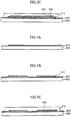
- FIGS. 3A to 3C are sectional views illustrating a method of manufacturing excitation and detection transducers for a touch screen panel according to another embodiment of the present invention.
- This embodiment describes a method of manufacturing excitation and detection transducers using the surface waveguiding effect of a Rayleigh (i.e., surface acoustic) wave to simplify a process in which a piezoelectric layer is formed on a substrate and, thereafter, symmetrical interdigital electrodes are formed on the same substrate.
- the excited detection frequency preferentially propagate along the top planar surface, and minimizes the excitation of waves in the thickness direction of the substrate. This results in the advantage that the substrate may be relatively thin, and acoustic energy is effectively concentrated at the surface of the display substrate.
- a piezoelectric layer 610 made of AlN, ZnO, LiNbO 3 , PZT etc., is formed on the predetermined area on the front surface of a substrate, which may be flexible rigid, using a sputtering method.
- Piezoelectric layer 610 may be formed using a method of performing patterning using a metal mask simultaneously at the time of deposition, or a method of performing patterning using a photolithography and etching process (wet or dry etching) after sputtering, as described above.
- a photolithography and etching process wet or dry etching
- one may use the method of patterning using an UV laser, described above.
- a metallic layers 620 may be formed on piezoelectric layer 610 such that the sides thereof are spaced apart from each other by a predetermined interval, thereby forming primary and secondary electrodes.
- Metallic layer 620 is formed by depositing a low-resistance metallic layer, made of Al, Cu, Ag, Au, ITO, IZO, etc. Electrode forming may be accomplished using a metal mask during a sputtering process without additionally requiring an etching process as described above. Alternatively, one may form electrodes using a method of direct etching by using a UV laser after the deposition of the film. Alternatively, a method of patterning using a photolithography and etching (wet or dry etching) process may be used. With any method, a predetermined area of piezoelectric layer 610 is exposed, and primary and secondary electrodes, which are spaced apart from each other by a predetermined interval, are formed.
- a protective layer 630 may be selectively made of SiO 2 material.
- electrode structures used as the frequency generation reception units may be manufactured.
- the method of manufacturing a touch screen panel in particular, the excitation transducer and the frequency reception unit, has been described with reference to the sectional views of FIGS. 2A to 2C and FIGS. 3A to 3C .
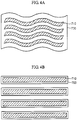
- the excitation and detection transducers may be manufactured in the same substrate in a line-form planar structure, which will be described with reference to FIGS. 4A and 4B .
- FIG. 4A is a diagram illustrating a planar layout in which a plurality of excitation and detection transducers 710 are simultaneously formed on a flexible substrate 700.
- the excitation and detection transducers 710 in which a primary electrode, a piezoelectric layer and a secondary electrode are formed on flexible substrate 700, and may be manufactured in a plurality of line forms in consideration of the size of the non-display zone of the image display unit.
- the excitation transducer and the frequency reception unit may be respectively segmented at predetermined regular intervals, and may then be attached to the front surface of the non-display zone of the image display unit, thereby enabling the manufacture of the ultrasonic wave detection-type touch screen panel.
- the method of manufacturing the excitation and detection transducers on a flexible substrate may be the same as described above, comprising the formation of electrodes and piezoelectric layer, and will not be repeated here in detail.
- a method of manufacturing the ultrasonic wave detection-type touch screen, in particular, the frequency generation unit and the frequency reception unit, which are formed on the flexible substrate may include forming a low-resistance metallic layer through sputtering, forming primary and secondary electrodes by patterning using an UV laser, then automatically patterning a piezoelectric layer made of ceramic by deposition through a metal mask, or by patterning using a photolithography and etching process.
- a method is described with reference to FIGS. 5A to 5D of sequentially attaching the excitation and detection transducers, described above (either flexible or rigid), to the non-display zone of the image display.
- a Y-directional excitation transducer 100 is attached to the left portion of the non-display zone of the image display unit and an X-directional detection transducer 200 is then attached to the lower portion of the non-display zone of the image display unit.
- an X-directional excitation transducer 300 is attached to the upper portion of the non-display zone of the image display unit, and a Y-directional detection transducer 400 is then attached to the right portion of the non-display zone of the image display unit, thereby manufacturing the ultrasonic wave detection-type touch screen panel.
- the entire substrate may be attached as a single layer structure to the image display unit.
- the substrate may be quite thin, there is substantially no adverse affect on the thickness of the overall display.
- one may separate only desired portions of the excitation and detection transducers from the substrate and attach them separately appropriately it to the non-display zone portions, and attach the remaining substrate and remaining excitation and detection transducers appropriately to the remaining non-display zone portions.
- the part of the image display unit, to which the excitation and detection transducers are attached may finally be packaged using an external bezel when the display is assembled, thereby providing a structure whereby excitation and detection transducers are not exposed to the outside.
- an optional protective layer made of SiO 2 , may be formed over the entire surface of the display unit which is also capable of propagating surface acoustic waves after the formation of a secondary electrode.
- FIGS. 6A and 6B are partial sectional views illustrating various modifications to the process for forming a polarizer of an LCD having the touch screen panel according to an embodiment of the present invention, and illustrate arrangements in which the excitation and detection transducers are attached to the border of the front surface of a color filter substrate.
- An example is given in which the excitation and detection transducers are formed by first forming a piezoelectric layer and then forming a single metallic layer, which are spaced apart from each other, thereby forming primary and secondary electrodes.
- the touch screen panel is not limited to being attached to the color filter substrate, and may be attached to a film transistor substrate.
- a sealant 1300 for attaching two substrates to each other is formed between a thin-film transistor substrate 1000, on which thin-film transistors and pixel electrodes are formed in a matrix arrangement, and a red-green-blue (RGB) color filter substrate 1100 is formed.
- a polarizer 1400 is formed on the surface of color filter substrate 1100.
- Polarizer 1400 may be a metal wire rigid polarizer or a lyotropic liquid crystal polymer-type internal polarizer.
- a polarizer is formed between the thin-film transistor substrate 1000 and a backlight unit below the thin-film transistor substrate 1000.
- excitation transducer 100 and a detection transducer 200 are attached to the border of the front surface of color filter substrate 1100.
- Each of excitation and detection transducers 100 and 200 is formed of a piezoelectric layer 1600, a primary electrode 1610 and a secondary electrode 1620 formed by a single metallic layer, the sides of which are spaced apart from each other, and a protective layer 1630 formed on the front surface thereof, using the process illustrated in FIGS. 3A to 3C . They may be formed on substrate 700 as illustrated in FIG. 4A , and may be segmented as illustrated in FIG. 4B , and may then be attached using adhesive members.
- a first polarizer 1400 may be formed on the surface of thin-film substrate 1000, on which a predetermined structure is formed, and a second polarizer 1410 is formed on the surface of color filter substrate 1100.
- first and second polarizers 1400 and 1410 may be a metal wire rigid polarizer or a lyotropic liquid crystal polymer-type internal polarizer.
- excitation transducer 100 and detection transducer 200 are attached to the border of the front surface of the color filter substrate 1100 using the above-described method.
- the excitation and detection transducers are attached to the front surface of the color filter substrate, so that the color filter substrate is used as surface acoustic wave propagation medium.
- the polarizer may be included on the opposite surface of a substrate or an LCD panel on which the ultrasonic wave detection-type touch screen panel is operational.
- a metal wire rigid polarizer or a lyotropic liquid crystal polymer-type internal polarizer may be used as the polarizer.
- ultrasonic wave detection-type touch screen panel has been described as applied an LCD as one example among planar display devices, it is not limited to such, and may also be applied to other planar display device, such as Organic Light Emitting Diode Displays (OLEDDs), or Plasma Display Panels (PDPs).
- OLEDDs Organic Light Emitting Diode Displays
- PDPs Plasma Display Panels
- the excitation and detection transducers may be attached to the outer surface of a substrate for manufacture of drive circuits or a back substrate, thereby forming a touch screen panel.
- the excitation and detection transducers may be attached to the outer surface of the front plate which normally contains display electrodes on the inside surface, thereby forming a touch screen panel.
- a touch screen panel is implemented by attaching excitation and detection transducers to the border of the front surface of an image display unit, and, the outer surface of the substrate of the display is used as a surface acoustic wave propagation medium. Therefore, since it is not required to manufacture a touch screen panel on a separate substrate, and attach the touch screen panel to the image display unit, image quality is not only maintained, but the thickness and size of displays thereof are also kept from increasing, as compared to implementations in the prior art.
- the touch screen panel is applied to a large display device or a mobile display device, the thickness and size of the display are not affected.
- the excitation and detection transducers may be cut at predetermined regular intervals and attached, so that the ultrasonic wave detection-type touch screen panel can be applied to any size large television or other large electronic display panel by extending the number of transducers.
- a process line for production of substrates for touch screen panels requires the size of the touch screen panel to be substantially identical to that of the display.
- the present invention does not require such a process line matching the size of every conceivable display size, thereby reducing manufacturing cost.
Landscapes
- Engineering & Computer Science (AREA)
- General Engineering & Computer Science (AREA)
- Theoretical Computer Science (AREA)
- Physics & Mathematics (AREA)
- Human Computer Interaction (AREA)
- General Physics & Mathematics (AREA)
- Acoustics & Sound (AREA)
- Position Input By Displaying (AREA)
Applications Claiming Priority (1)
| Application Number | Priority Date | Filing Date | Title |
|---|---|---|---|
| KR1020060073433A KR101303881B1 (ko) | 2006-08-03 | 2006-08-03 | 터치 스크린, 그 제조 방법 및 이를 구비하는 표시 장치 |
Publications (3)
| Publication Number | Publication Date |
|---|---|
| EP1892610A2 EP1892610A2 (en) | 2008-02-27 |
| EP1892610A3 EP1892610A3 (en) | 2012-11-14 |
| EP1892610B1 true EP1892610B1 (en) | 2018-02-21 |
Family
ID=38544323
Family Applications (1)
| Application Number | Title | Priority Date | Filing Date |
|---|---|---|---|
| EP07014985.1A Active EP1892610B1 (en) | 2006-08-03 | 2007-07-31 | Touch screen panel, method of manufacturing the same, and display having the same |
Country Status (6)
| Country | Link |
|---|---|
| US (1) | US8451231B2 (ja) |
| EP (1) | EP1892610B1 (ja) |
| JP (1) | JP5228150B2 (ja) |
| KR (1) | KR101303881B1 (ja) |
| CN (1) | CN101140371A (ja) |
| TW (1) | TWI403943B (ja) |
Families Citing this family (38)
| Publication number | Priority date | Publication date | Assignee | Title |
|---|---|---|---|---|
| US20090267891A1 (en) * | 2008-04-25 | 2009-10-29 | Bamidele Ali | Virtual paper |
| CN101587395B (zh) * | 2008-05-23 | 2011-01-26 | 汉王科技股份有限公司 | 多模式坐标和压力输入装置及方法 |
| KR101011284B1 (ko) * | 2008-07-16 | 2011-01-28 | 성균관대학교산학협력단 | 투명 압전 소자 및 그 형성방법 |
| CN101685212B (zh) * | 2008-09-26 | 2012-08-29 | 群康科技(深圳)有限公司 | 液晶显示面板 |
| JP5252427B2 (ja) * | 2008-10-01 | 2013-07-31 | 株式会社ジャパンディスプレイウェスト | 入力装置および表示装置 |
| KR101013467B1 (ko) * | 2008-11-18 | 2011-02-14 | 삼성전기주식회사 | 촉감제시 터치스크린 및 이를 구비한 디스플레이 장치 |
| JP2010165032A (ja) * | 2009-01-13 | 2010-07-29 | Hitachi Displays Ltd | タッチパネルディスプレイ装置 |
| KR101139020B1 (ko) * | 2009-09-29 | 2012-04-26 | 엘지이노텍 주식회사 | 멀티 저항막 터치스크린 및 그 제조방법 |
| US20110128227A1 (en) * | 2009-11-30 | 2011-06-02 | Research In Motion Limited | Portable electronic device and method of controlling same to provide tactile feedback |
| JP5414546B2 (ja) * | 2010-01-12 | 2014-02-12 | キヤノン株式会社 | 容量検出型の電気機械変換素子 |
| TWI410702B (zh) * | 2010-02-10 | 2013-10-01 | Au Optronics Corp | 觸控顯示面板 |
| CN102844726A (zh) * | 2010-02-26 | 2012-12-26 | 惠普发展公司,有限责任合伙企业 | 用于提供触摸反馈的触觉显示器 |
| CN102236484B (zh) * | 2010-04-30 | 2015-03-11 | 永恒科技有限公司 | 图案化衬底的方法及制造电容式触控面板的方法 |
| JP5355515B2 (ja) * | 2010-05-06 | 2013-11-27 | 株式会社村田製作所 | タッチパネル、ならびにタッチ式入力装置およびその制御方法 |
| US11327599B2 (en) | 2011-04-26 | 2022-05-10 | Sentons Inc. | Identifying a contact type |
| KR101820014B1 (ko) * | 2011-09-09 | 2018-01-19 | 삼성디스플레이 주식회사 | 터치 패널 및 터치 패널의 접촉 정보 판단 방법 |
| US8456575B2 (en) * | 2011-09-21 | 2013-06-04 | Sony Corporation | Onscreen remote control presented by audio video display device such as TV to control source of HDMI content |
| CN102339166A (zh) * | 2011-10-12 | 2012-02-01 | 清华大学 | 可折叠、可柔性变形的压电触摸屏 |
| CN103105962B (zh) * | 2011-11-09 | 2016-04-06 | 宸鸿科技(厦门)有限公司 | 触控面板、触控电极结构及其制作方法 |
| US20210294457A1 (en) * | 2011-11-18 | 2021-09-23 | Sentons Inc. | Ultrasonic detection of change in pressure on an adhesive interface |
| US9099971B2 (en) | 2011-11-18 | 2015-08-04 | Sentons Inc. | Virtual keyboard interaction using touch input force |
| BR112014019107B1 (pt) * | 2012-02-02 | 2021-05-04 | Qualcomm Incorporated | Monitor com tela sensível ao toque e método para coletar informação sobre um objeto que está em contato com um monitor com tela sensível ao toque |
| WO2013119868A1 (en) * | 2012-02-07 | 2013-08-15 | Ritedia Corporation | LIGHT TRANSMITTIVE AlN LAYERS AND ASSOCIATED DEVICES AND METHODS |
| TW201335817A (zh) * | 2012-02-21 | 2013-09-01 | Ritedia Corp | 表面聲波式觸控面板及其製造方法 |
| CN103309528A (zh) * | 2012-03-16 | 2013-09-18 | 瀚宇彩晶股份有限公司 | 触控面板及其制作方法 |
| US20140293168A1 (en) * | 2012-06-06 | 2014-10-02 | Wintek Corporation | Touch panel |
| US20140009429A1 (en) * | 2012-07-03 | 2014-01-09 | Chimei Innolux Corporation | Method of producing capacitive coplanar touch panel devices with laser ablation |
| US8890853B2 (en) | 2013-01-11 | 2014-11-18 | Sharp Laboratories Of America, Inc. | In-pixel ultrasonic touch sensor for display applications |
| KR101459461B1 (ko) * | 2013-05-20 | 2014-11-10 | 현대자동차 주식회사 | 아날로그 조작장치를 구비하는 터치 스크린 입력 시스템 |
| KR20150086763A (ko) * | 2014-01-20 | 2015-07-29 | 삼성디스플레이 주식회사 | 발광형 표시장치 및 그 제조방법 |
| CN105718105B (zh) * | 2015-12-25 | 2018-12-11 | 业成科技(成都)有限公司 | 有机发光二极管触控显示面板 |
| CN107422892A (zh) * | 2016-05-23 | 2017-12-01 | 中兴通讯股份有限公司 | 一种屏幕模组触控方法、装置及终端 |
| CN106530968B (zh) * | 2016-12-27 | 2019-09-20 | 京东方科技集团股份有限公司 | 显示装置和显示装置的控制方法 |
| US11580829B2 (en) | 2017-08-14 | 2023-02-14 | Sentons Inc. | Dynamic feedback for haptics |
| FR3081907B1 (fr) * | 2018-05-31 | 2022-03-04 | Saint Gobain | Vitrage ayant des performances acoustiques ameliorees |
| TWI697828B (zh) * | 2018-11-29 | 2020-07-01 | 宏碁股份有限公司 | 具備超音波觸控的電子裝置 |
| CN112286394B (zh) * | 2020-10-30 | 2024-02-09 | 武汉天马微电子有限公司 | 显示面板及显示装置 |
| CN112181208B (zh) * | 2020-10-30 | 2023-06-02 | 业泓科技(成都)有限公司 | 触控辨识装置、显示装置及其制造方法 |
Family Cites Families (39)
| Publication number | Priority date | Publication date | Assignee | Title |
|---|---|---|---|---|
| US4777329A (en) | 1987-08-24 | 1988-10-11 | Microfield Graphics, Inc. | Graphic input system |
| US5308936A (en) | 1992-08-26 | 1994-05-03 | Mark S. Knighton | Ultrasonic pen-type data input device |
| TW241352B (en) * | 1994-03-30 | 1995-02-21 | Whitaker Corp | Reflective mode ultrasonic touch sensitive switch |
| US5657054A (en) * | 1995-04-26 | 1997-08-12 | Texas Instruments Incorporated | Determination of pen location on display apparatus using piezoelectric point elements |
| JPH0922324A (ja) * | 1995-07-05 | 1997-01-21 | Canon Inc | 座標入力装置 |
| US6292177B1 (en) | 1997-03-05 | 2001-09-18 | Tidenet, Inc. | Marking device for electronic presentation board |
| US6087599A (en) | 1997-11-24 | 2000-07-11 | The Whitaker Corporation | Touch panels having plastic substrates |
| GB9818827D0 (en) * | 1998-08-29 | 1998-10-21 | Ncr Int Inc | Surface wave touch screen |
| US6731270B2 (en) | 1998-10-21 | 2004-05-04 | Luidia Inc. | Piezoelectric transducer for data entry device |
| JP3717034B2 (ja) | 1998-11-10 | 2005-11-16 | 株式会社村田製作所 | 弾性表面波素子 |
| IL129450A (en) | 1999-04-14 | 2004-09-27 | Pegasus Technologies Ltd | Digitizer for erasable white whiteboards |
| KR100534376B1 (ko) * | 1999-06-21 | 2005-12-08 | 엘지.필립스 엘시디 주식회사 | 디지타이저를 가진 액정표시소자 |
| JP2001014094A (ja) * | 1999-06-30 | 2001-01-19 | Touch Panel Systems Kk | 音響的接触検出装置 |
| JP4785247B2 (ja) * | 2000-12-19 | 2011-10-05 | 耕司 戸田 | 超音波接触位置検出装置 |
| JP4562294B2 (ja) * | 2001-01-26 | 2010-10-13 | 富士通株式会社 | タッチパネル装置 |
| CN2519331Y (zh) | 2002-01-30 | 2002-10-30 | 成都吉锐触摸电脑有限公司 | 通过触摸区域级连增大有效触摸区的表面声波触摸屏 |
| JP4376474B2 (ja) * | 2001-04-17 | 2009-12-02 | グンゼ株式会社 | 透明導電性フィルム |
| JP2002342027A (ja) | 2001-05-14 | 2002-11-29 | Seiko Instruments Inc | タッチセンシング機能付き表示装置 |
| JP4527315B2 (ja) * | 2001-05-14 | 2010-08-18 | セイコーインスツル株式会社 | 表示装置 |
| AUPR507601A0 (en) | 2001-05-21 | 2001-06-14 | Microtechnology Centre Management Limited | Surface acoustic wave sensor |
| JP2003029930A (ja) * | 2001-07-17 | 2003-01-31 | Fujikura Ltd | タッチパネル及びその製造方法 |
| JP3871547B2 (ja) * | 2001-10-23 | 2007-01-24 | 富士通株式会社 | タッチパネル装置 |
| JP4052884B2 (ja) * | 2002-06-24 | 2008-02-27 | 富士通株式会社 | タッチパネル装置 |
| JP2004054485A (ja) * | 2002-07-18 | 2004-02-19 | Seiko Instruments Inc | 表示装置 |
| US7292848B2 (en) * | 2002-07-31 | 2007-11-06 | General Motors Corporation | Method of activating an in-vehicle wireless communication device |
| JP2004078613A (ja) | 2002-08-19 | 2004-03-11 | Fujitsu Ltd | タッチパネル装置 |
| JP3937982B2 (ja) | 2002-08-29 | 2007-06-27 | ソニー株式会社 | 入出力装置および入出力装置を有する電子機器 |
| JP2004127073A (ja) * | 2002-10-04 | 2004-04-22 | Smk Corp | 指示入力装置 |
| JP2004163262A (ja) * | 2002-11-13 | 2004-06-10 | Touch Panel Systems Kk | 音響波型接触検出装置 |
| JP4095068B2 (ja) | 2003-05-22 | 2008-06-04 | 富士通株式会社 | 圧電素子、その製造方法、およびタッチパネル装置 |
| JP4198527B2 (ja) | 2003-05-26 | 2008-12-17 | 富士通コンポーネント株式会社 | タッチパネル及び表示装置 |
| JP2004355092A (ja) | 2003-05-27 | 2004-12-16 | Sony Corp | タッチパネル付表示装置とその製造方法 |
| JP4359757B2 (ja) | 2003-09-17 | 2009-11-04 | ソニー株式会社 | 情報表示装置 |
| KR100533642B1 (ko) | 2004-03-29 | 2005-12-06 | 삼성전기주식회사 | 표면탄성파를 이용한 터치 위치 감지 장치 |
| US8325159B2 (en) * | 2004-04-14 | 2012-12-04 | Elo Touch Solutions, Inc. | Acoustic touch sensor |
| JP4593198B2 (ja) | 2004-08-05 | 2010-12-08 | 富士通コンポーネント株式会社 | タッチパネルおよびタッチパネルの製造方法 |
| JP4357389B2 (ja) * | 2004-08-20 | 2009-11-04 | 富士通株式会社 | タッチパネル装置およびその製造方法 |
| JP2006099608A (ja) | 2004-09-30 | 2006-04-13 | Touch Panel Systems Kk | 接触検出機能付き表示装置 |
| KR100802882B1 (ko) | 2005-11-18 | 2008-02-13 | 후지쯔 가부시끼가이샤 | 압전 소자, 그 제조 방법 및 터치 패널 장치 |
-
2006
- 2006-08-03 KR KR1020060073433A patent/KR101303881B1/ko active IP Right Grant
-
2007
- 2007-02-21 JP JP2007040410A patent/JP5228150B2/ja active Active
- 2007-07-31 EP EP07014985.1A patent/EP1892610B1/en active Active
- 2007-08-02 US US11/888,933 patent/US8451231B2/en active Active
- 2007-08-02 TW TW096128376A patent/TWI403943B/zh active
- 2007-08-03 CN CNA2007101676774A patent/CN101140371A/zh active Pending
Non-Patent Citations (1)
| Title |
|---|
| None * |
Also Published As
| Publication number | Publication date |
|---|---|
| TWI403943B (zh) | 2013-08-01 |
| KR20080012513A (ko) | 2008-02-12 |
| KR101303881B1 (ko) | 2013-09-04 |
| CN101140371A (zh) | 2008-03-12 |
| JP5228150B2 (ja) | 2013-07-03 |
| EP1892610A3 (en) | 2012-11-14 |
| US8451231B2 (en) | 2013-05-28 |
| TW200820055A (en) | 2008-05-01 |
| EP1892610A2 (en) | 2008-02-27 |
| US20080030483A1 (en) | 2008-02-07 |
| JP2008041077A (ja) | 2008-02-21 |
Similar Documents
| Publication | Publication Date | Title |
|---|---|---|
| EP1892610B1 (en) | Touch screen panel, method of manufacturing the same, and display having the same | |
| US8952929B2 (en) | Touch display, liquid crystal display with a built-in touch | |
| CN113407070B (zh) | 触摸液晶显示装置及其制造方法 | |
| KR101896377B1 (ko) | 베젤이 최소화된 액정표시소자 | |
| US20070229479A1 (en) | Panel assembly | |
| KR20150078248A (ko) | 표시소자 | |
| TW201327304A (zh) | 觸控顯示面板 | |
| JP2007310885A (ja) | 表示パネル | |
| JP5940163B2 (ja) | 半導体装置及び表示装置 | |
| US20200348784A1 (en) | Touch display substrate, method of manufacturing the same and display device | |
| JP2011159094A (ja) | 電気的固体装置の製造方法 | |
| KR101432891B1 (ko) | 액정표시장치 | |
| JP2012088599A (ja) | タッチセンサ機能付き液晶表示装置 | |
| JP4593198B2 (ja) | タッチパネルおよびタッチパネルの製造方法 | |
| JP2005275054A (ja) | 液晶表示装置および液晶表示装置の製造方法 | |
| KR101818453B1 (ko) | 액정 표시 장치 및 이의 제조 방법 | |
| JPH1195255A (ja) | 液晶表示装置のアレイ基板、およびこれを備えた液晶表示装置 | |
| JP2007225644A (ja) | 電気光学装置の製造方法、電気光学装置、及び電子機器 | |
| JPH08179306A (ja) | 表示装置 | |
| KR100308155B1 (ko) | 액정표시소자및그제조방법 | |
| KR102293566B1 (ko) | 터치 센서 및 이를 포함하는 화상 표시 장치 | |
| KR20120075109A (ko) | 프린지 필드형 액정표시장치 및 그 제조방법 | |
| JP4222051B2 (ja) | 液晶表示装置 | |
| KR100928481B1 (ko) | 액정표시장치의 제조방법 | |
| JP2000155323A (ja) | 液晶表示装置 |
Legal Events
| Date | Code | Title | Description |
|---|---|---|---|
| PUAI | Public reference made under article 153(3) epc to a published international application that has entered the european phase |
Free format text: ORIGINAL CODE: 0009012 |
|
| AK | Designated contracting states |
Kind code of ref document: A2 Designated state(s): AT BE BG CH CY CZ DE DK EE ES FI FR GB GR HU IE IS IT LI LT LU LV MC MT NL PL PT RO SE SI SK TR |
|
| AX | Request for extension of the european patent |
Extension state: AL BA HR MK YU |
|
| RAP1 | Party data changed (applicant data changed or rights of an application transferred) |
Owner name: SAMSUNG ELECTRONICS CO., LTD. |
|
| PUAL | Search report despatched |
Free format text: ORIGINAL CODE: 0009013 |
|
| RAP1 | Party data changed (applicant data changed or rights of an application transferred) |
Owner name: SAMSUNG DISPLAY CO., LTD. |
|
| AK | Designated contracting states |
Kind code of ref document: A3 Designated state(s): AT BE BG CH CY CZ DE DK EE ES FI FR GB GR HU IE IS IT LI LT LU LV MC MT NL PL PT RO SE SI SK TR |
|
| AX | Request for extension of the european patent |
Extension state: AL BA HR MK RS |
|
| RIC1 | Information provided on ipc code assigned before grant |
Ipc: G06F 3/043 20060101AFI20121010BHEP |
|
| 17P | Request for examination filed |
Effective date: 20130107 |
|
| AKX | Designation fees paid |
Designated state(s): FR GB NL |
|
| REG | Reference to a national code |
Ref country code: DE Ref legal event code: R108 |
|
| REG | Reference to a national code |
Ref country code: DE Ref legal event code: R108 Effective date: 20130717 |
|
| RAP1 | Party data changed (applicant data changed or rights of an application transferred) |
Owner name: SAMSUNG DISPLAY CO., LTD. |
|
| 17Q | First examination report despatched |
Effective date: 20160620 |
|
| GRAP | Despatch of communication of intention to grant a patent |
Free format text: ORIGINAL CODE: EPIDOSNIGR1 |
|
| INTG | Intention to grant announced |
Effective date: 20171011 |
|
| GRAS | Grant fee paid |
Free format text: ORIGINAL CODE: EPIDOSNIGR3 |
|
| GRAA | (expected) grant |
Free format text: ORIGINAL CODE: 0009210 |
|
| AK | Designated contracting states |
Kind code of ref document: B1 Designated state(s): FR GB NL |
|
| REG | Reference to a national code |
Ref country code: GB Ref legal event code: FG4D |
|
| REG | Reference to a national code |
Ref country code: NL Ref legal event code: MP Effective date: 20180221 |
|
| PG25 | Lapsed in a contracting state [announced via postgrant information from national office to epo] |
Ref country code: NL Free format text: LAPSE BECAUSE OF FAILURE TO SUBMIT A TRANSLATION OF THE DESCRIPTION OR TO PAY THE FEE WITHIN THE PRESCRIBED TIME-LIMIT Effective date: 20180221 |
|
| PLBE | No opposition filed within time limit |
Free format text: ORIGINAL CODE: 0009261 |
|
| STAA | Information on the status of an ep patent application or granted ep patent |
Free format text: STATUS: NO OPPOSITION FILED WITHIN TIME LIMIT |
|
| 26N | No opposition filed |
Effective date: 20181122 |
|
| PG25 | Lapsed in a contracting state [announced via postgrant information from national office to epo] |
Ref country code: FR Free format text: LAPSE BECAUSE OF NON-PAYMENT OF DUE FEES Effective date: 20180731 |
|
| P01 | Opt-out of the competence of the unified patent court (upc) registered |
Effective date: 20230515 |
|
| PGFP | Annual fee paid to national office [announced via postgrant information from national office to epo] |
Ref country code: GB Payment date: 20230620 Year of fee payment: 17 |