EP1865713B1 - Dispositif de prise de vues de type oeil à facettes - Google Patents
Dispositif de prise de vues de type oeil à facettes Download PDFInfo
- Publication number
- EP1865713B1 EP1865713B1 EP07011279A EP07011279A EP1865713B1 EP 1865713 B1 EP1865713 B1 EP 1865713B1 EP 07011279 A EP07011279 A EP 07011279A EP 07011279 A EP07011279 A EP 07011279A EP 1865713 B1 EP1865713 B1 EP 1865713B1
- Authority
- EP
- European Patent Office
- Prior art keywords
- light
- passing
- unit plates
- imaging device
- compound
- Prior art date
- Legal status (The legal status is an assumption and is not a legal conclusion. Google has not performed a legal analysis and makes no representation as to the accuracy of the status listed.)
- Not-in-force
Links
- 238000003384 imaging method Methods 0.000 title claims description 50
- 230000003287 optical effect Effects 0.000 claims description 77
- 230000001788 irregular Effects 0.000 claims description 19
- 239000011159 matrix material Substances 0.000 claims description 10
- 238000000149 argon plasma sintering Methods 0.000 claims description 9
- 230000002452 interceptive effect Effects 0.000 claims description 6
- 238000000638 solvent extraction Methods 0.000 claims description 5
- 125000006850 spacer group Chemical group 0.000 description 12
- 238000000034 method Methods 0.000 description 4
- 239000002184 metal Substances 0.000 description 3
- 229910052751 metal Inorganic materials 0.000 description 3
- 238000005192 partition Methods 0.000 description 3
- 239000000758 substrate Substances 0.000 description 3
- XEEYBQQBJWHFJM-UHFFFAOYSA-N Iron Chemical compound [Fe] XEEYBQQBJWHFJM-UHFFFAOYSA-N 0.000 description 2
- 239000000853 adhesive Substances 0.000 description 2
- 230000001070 adhesive effect Effects 0.000 description 2
- 230000003247 decreasing effect Effects 0.000 description 2
- 238000005530 etching Methods 0.000 description 2
- 238000004519 manufacturing process Methods 0.000 description 2
- 239000000463 material Substances 0.000 description 2
- 238000012986 modification Methods 0.000 description 2
- 230000004048 modification Effects 0.000 description 2
- 230000004075 alteration Effects 0.000 description 1
- 230000015572 biosynthetic process Effects 0.000 description 1
- 230000001413 cellular effect Effects 0.000 description 1
- 238000005553 drilling Methods 0.000 description 1
- 229910052742 iron Inorganic materials 0.000 description 1
- 238000012634 optical imaging Methods 0.000 description 1
- 239000011347 resin Substances 0.000 description 1
- 229920005989 resin Polymers 0.000 description 1
- 239000004065 semiconductor Substances 0.000 description 1
- 239000000126 substance Substances 0.000 description 1
Images


Classifications
-
- G—PHYSICS
- G02—OPTICS
- G02B—OPTICAL ELEMENTS, SYSTEMS OR APPARATUS
- G02B3/00—Simple or compound lenses
- G02B3/0006—Arrays
- G02B3/0075—Arrays characterized by non-optical structures, e.g. having integrated holding or alignment means
-
- H—ELECTRICITY
- H04—ELECTRIC COMMUNICATION TECHNIQUE
- H04N—PICTORIAL COMMUNICATION, e.g. TELEVISION
- H04N23/00—Cameras or camera modules comprising electronic image sensors; Control thereof
- H04N23/50—Constructional details
- H04N23/54—Mounting of pick-up tubes, electronic image sensors, deviation or focusing coils
-
- H—ELECTRICITY
- H04—ELECTRIC COMMUNICATION TECHNIQUE
- H04N—PICTORIAL COMMUNICATION, e.g. TELEVISION
- H04N23/00—Cameras or camera modules comprising electronic image sensors; Control thereof
- H04N23/57—Mechanical or electrical details of cameras or camera modules specially adapted for being embedded in other devices
-
- H—ELECTRICITY
- H10—SEMICONDUCTOR DEVICES; ELECTRIC SOLID-STATE DEVICES NOT OTHERWISE PROVIDED FOR
- H10F—INORGANIC SEMICONDUCTOR DEVICES SENSITIVE TO INFRARED RADIATION, LIGHT, ELECTROMAGNETIC RADIATION OF SHORTER WAVELENGTH OR CORPUSCULAR RADIATION
- H10F39/00—Integrated devices, or assemblies of multiple devices, comprising at least one element covered by group H10F30/00, e.g. radiation detectors comprising photodiode arrays
- H10F39/80—Constructional details of image sensors
- H10F39/805—Coatings
- H10F39/8057—Optical shielding
-
- G—PHYSICS
- G02—OPTICS
- G02B—OPTICAL ELEMENTS, SYSTEMS OR APPARATUS
- G02B3/00—Simple or compound lenses
- G02B3/0006—Arrays
-
- G—PHYSICS
- G02—OPTICS
- G02B—OPTICAL ELEMENTS, SYSTEMS OR APPARATUS
- G02B3/00—Simple or compound lenses
- G02B3/0006—Arrays
- G02B3/0037—Arrays characterized by the distribution or form of lenses
- G02B3/0056—Arrays characterized by the distribution or form of lenses arranged along two different directions in a plane, e.g. honeycomb arrangement of lenses
-
- H—ELECTRICITY
- H10—SEMICONDUCTOR DEVICES; ELECTRIC SOLID-STATE DEVICES NOT OTHERWISE PROVIDED FOR
- H10F—INORGANIC SEMICONDUCTOR DEVICES SENSITIVE TO INFRARED RADIATION, LIGHT, ELECTROMAGNETIC RADIATION OF SHORTER WAVELENGTH OR CORPUSCULAR RADIATION
- H10F39/00—Integrated devices, or assemblies of multiple devices, comprising at least one element covered by group H10F30/00, e.g. radiation detectors comprising photodiode arrays
- H10F39/80—Constructional details of image sensors
- H10F39/806—Optical elements or arrangements associated with the image sensors
- H10F39/8063—Microlenses
Definitions
- the present invention relates to a compound-eye imaging device having an optical imaging system which is formed of multiple micro optical systems so as to reduce the focal length, making it possible to reduce the thickness of the compound-eye imaging device.
- the compound-eye imaging device is mainly composed of: an optical lens array with multiple integrated optical lenses; a photodetector array for imaging multiple images formed by the respective optical lenses of the optical lens array; and an image reconstructing circuit for reconstructing the multiple images, imaged by the photodetector array, into one image by using parallax information between the multiple images.
- FIG. 10 is a schematic vertical cross-sectional view of a conventional compound-eye imaging device 100, showing a general structure of a conventional compound-eye imaging device. The structure of the conventional compound-eye imaging device 100 will be described with reference to FIG 10 .
- the compound-eye imaging device 100 comprises: an optical lens array 104 with integrally formed multiple optical lenses 102; a stop member 111 for shielding unnecessary ambient light from entering the optical lenses 102; a photodetector array 106 placed at a predetermined distance from the optical lens array 104 for imaging multiple images respectively formed by the optical lenses 102; and a light shielding block 107 which is placed between the optical lens array 104 and the photodetector array 106, and which has a partition wall for partitioning a space between the optical lens array 104 and the photodetector array 106 into a matrix of spaces as seen on a plane perpendicular to an optical axis L of each optical lens 102 so as to prevent lights emitted from the respective optical lenses 102 from interfering each other.
- the optical lens array 104 is held by a lens holder 105.
- the shielding block 107 is formed of a plate-like or flat plate material having a predetermined thickness and having formed therein multiple light-passing holes H which face the respective optical lenses 102. In one way, laser processing is used to form such light-passing holes H in a metal plate. Otherwise, in some cases, a plate-like or flat plate material formed by a photo-curable resin may be used for the light shielding block 107.
- the conventional compound-eye imaging device 100 there is a problem in the quality of formed images. More specifically, as shown by a bent arrow A in FIG. 10 , some of the lights emitted from the optical lenses 102, which are expected to directly arrive at the photodetector array 106, may first arrive at an inner wall surface Ha of a light-passing hole H, so as to be reflected by the inner wall surface Ha and then arrive at the photodetector array 106. Because of the existence of both the direct and reflected lights from the optical lenses 102, there is a risk of occurrence of ghost or flare in an image formed by the photodetector array 106.
- EP-A-0 813 079 relates to a short focal length image senior Figure 4 of EP-A-0 813 079 illustrates a lenslet array positioned over an image photosensor array having a number of photosensitive sites corresponding in number to at least the number of lenslets forming the lenslet array, wherein the lenslet array is maintained a distance apart from the surfaces of the photosensors by spacers.
- An aperture stop array in combination with the spacers and a field stop array limit the field of view of any particular photosensor so that it does not overlap the field of view of it neighbors by a large amount.
- EP-A-1 079 613 relates to an image input apparatus in which a single plane photosensitive element array is divided into areas each corresponding to one microlens so that each area includes a plurality of photosensitive elements, and in addition partition walls are provided to prevent interference among the optical signals from the individual microlenses.
- An object of the present invention is to provide a compound-eye imaging device which can prevent lights emitted from optical lenses from being reflected by an inner wall surface of a light-passing hole formed in a light shielding block and arriving at a photodetector array so as to cause ghost or flare in an image formed by the photodetector array.
- a compound-eye imaging device comprising: an optical lens array with multiple integrated optical lenses; a stop member for shielding unnecessary ambient light from entering the optical lenses; a photodetector array placed at a predetermined distance from the optical lens array for imaging images formed by the optical lenses, respectively; and a light shielding block placed between the optical lens array and the photodetector array for partitioning a space between the optical lens array and the photodetector array into a matrix of spaces, with light-passing holes, as seen on a plane perpendicular to the optical axis of each optical lens so as to prevent lights emitted from the optical lenses from interfering each other.
- the light shielding block is formed of a stack of multiple unit plates, each of which has multiple light-passing windows at horizontal positions thereon corresponding to horizontal positions of the optical lenses for passing lights emitted from the optical lenses so as to form the light-passing holes, respectively, wherein each of the light-passing holes formed by the light-passing windows in the unit plates in the stack has an irregular inner wall surface serving as a light scattering surface.
- the inner wall surface of each light-passing hole of the light shielding block is formed to be irregular or uneven to serve as a light scattering or irregularly reflecting surface.
- the inner wall surface prevents light reflected by the inner wall surface, among lights emitted from the optical lenses, from arriving at the photodetector array to form ghost (ghost image) and flare in an image formed on the photodetector array.
- this compound-eye imaging device makes it possible to use unit plates having the same shape, which are stacked by being alternately reversed upside down and left-right, so as to alternately offset the horizontal positions of the light-passing windows in each light-passing hole in the depth direction of the light-passing hole, thereby forming the irregular inner wall surface.
- this compound-eye imaging device enables the reduction of the manufacturing cost as compared to that in which different or multiple shapes of unit plates are used.
- the height of the light shielding block can be easily adjusted by changing (increasing or decreasing) the number of unit plates to form the light shielding block, so as to e.g. optimize the distance between the optical lens array and the photodetector array.
- each of the light-passing windows in each of the unit plates has blackened surface, wherein the unit plates in the stack are alternately reversed upside down and left-right so as to allow the horizontal positions of the light-passing windows for forming each light-passing hole through the unit plates in the stack to be alternately offset in depth direction of the each light-passing hole, thereby forming the irregular inner wall surface.
- each of the light-passing windows in each of the unit plates has blackened surface, wherein the light-passing windows of the unit plates in the stack have alternately different sizes so as to allow the horizontal positions of the light-passing windows for forming each light-passing hole through the unit plates in the stack to be alternately offset in depth direction of the each light-passing hole, thereby forming the irregular inner wall surface.
- each of the unit plates has a tapered surface on the inner wall surface in each of the light-passing windows therein so as to allow each light-passing hole through the unit plates in the stack to have the irregular inner wall surface.
- FIG. 1 is a schematic exploded perspective view of a compound-eye imaging device 1 according to the present embodiment when assembling the same in its entirety.
- FIG 2 is a schematic plan view of a light shielding block 7.
- FIG 3 and FIG 4 are schematic vertical cross-sectional views of the compound-eye imaging device 1 along line III-III and line IV-IV of FIG. 2 , respectively, showing, in addition to the light shielding block 7, a lens holder 5 and a photodetector array 6 in the compound-eye imaging device 1.
- the compound-eye imaging device 1 comprises: an optical lens array 4 having 9 (nine) optical lenses 2 which have optical axes L parallel to each other, and which are arranged in a matrix of three rows and three columns and integrally formed as single convex lenses on a lower surface of one transparent substrate 3; and a lens holder 5 for vertically sandwiching and holding the optical lens array 4.
- the compound-eye imaging device 1 further comprises: a photodetector array 6 which is placed below, and at a predetermined distance from, the optical lens array 4, and which images 9 (nine) images also arranged in a matrix of three rows and three columns formed by, and corresponding to, the 9 optical lenses 2; a light shielding block 7 which is placed between the optical lens array 4 and the photodetector array 6, and which has a partition wall for partitioning a space between the optical lens array 4 and the photodetector array 6 into a matrix (three rows and three columns) of spaces, with light-passing holes H, as seen on a plane perpendicular to the optical axis L so as to pass lights emitted from the respective optical lenses 2 and to prevent the lights from the optical lenses 2 from interfering each other; and a spacer frame 8 which is placed between the light shielding block 7 and the photodetector array 6, and surrounds the photodetector array 6 so as to prevent the light shielding block 7 from contacting the photodetector array
- the lens holder 5 is composed of an upper plate 11 and a lower frame 12 having grooves 12a formed in upper inner edges thereof, such that end portions 3a of the optical lens array 4 fit in the grooves 12a.
- the upper plate 11 has 9 (nine) stop apertures 11a having a predetermined size at 9 positions corresponding to the 9 optical lenses 2 so as to serve as a stop member for shielding unnecessary ambient light from entering the optical lenses 2.
- the photodetector array 6 shown in FIG. 1 is formed of a semiconductor substrate, and is, for example, a CCD (Charge Coupled Device) image sensor.
- the photodetector array 6 is mounted on a square portion 13a which is an end portion of a flexible board (circuit board) 13.
- the flexible board 13 has, at the other end portion thereof, terminals 14 of signal lines extending from the photodetector array (CCD) 6.
- the lens holder 5, the light shielding block 7, the spacer frame 8 and the square portion 13a of the flexible board 13 are formed in the same-sized square, and have circular through-holes 5a, 7a, 8a and 13b at four corners of each thereof for later-described positioning pins 100 to pass through, respectively.
- each of the light shielding block 7 and the spacer frame 8 has, in side surfaces thereof, recesses (notches) (not shown) in which an adhesive is to be filled, so as to facilitate bonding and fixedly connecting unit plates P (forming the shielding block 7) to each other as well as the spacer frame 8 and the light shielding block 7 to each other.
- the light shielding block 7 of the present embodiment is formed of 8 (eight) stacked flat unit plates P each having a thickness of 100 ⁇ m.
- Each of the unit plates P in the stack is formed e.g. of a metal plate such as an iron plate.
- the metal plate is subjected to an etching (chemical engraving) process capable of fine processing so as to form rectangular light-passing windows W having blackened surface.
- the light-passing windows W of each unit plate P are formed at horizontal positions on the each unit plate P corresponding to the horizontal positions of the multiple optical lenses 2, respectively, so as to pass lights emitted from the optical lenses 2.
- the light-passing windows W of each unit plate P in the stack are substantially vertically aligned with the corresponding light-passing windows W of the other unit plates P in the stack so that each set of substantially vertically light-passing windows W forms a light-passing hole H, thereby forming light-passing holes H, the number of which corresponds to the number of light-passing windows W of each unit plate P.
- the horizontal positions of the light-passing windows W for forming each light-passing hole H through the unit plates P in the stack are alternately offset (staggered) in depth direction of the each light-passing hole H, as seen through the stack in plan view, so as to form an irregular inner wall surface Ha as a light scattering surface.
- each light-passing hole H is arranged in a matrix and are thus partitioned from each other so as to prevent lights emitted from the respective optical lenses 2 from interfering each other.
- the unit plates P when stacked, are appropriately reversed horizontally (left-right) and vertically (upside down), so that the horizontal positions of the light-passing windows W for forming each light-passing hole H through the unit plates P in the stack are alternately offset (staggered) in depth direction of the each light-passing hole H as seen through the stack in plan view.
- each light-passing hole H has an irregular or uneven inner wall surface Ha serving as a light scattering surface. This will be described in detail below.
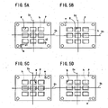
- FIG. 5A is a schematic plan view of an upper surface of a unit plate P in a basic state to be used for forming a light shielding block 7, in which Sv and Sh designate a longitudinal (up and down) center line and a lateral (left and right) center line, respectively.
- FIG. 5B is a schematic plan view of a lower surface of the unit plate P of FIG. 5A reversed upside down from that shown in FIG. 5A by rotating it 180 degrees about the lateral center line Sh.
- FIG. 5C is a schematic plan view of the upper surface of the unit plate P reversed left-right from that shown in FIG. 5B by rotating it 180 degrees about the longitudinal center line Sv
- FIG. 5D is a schematic plan view of the lower surface of the unit plate P reversed upside down from that shown in FIG. 5C by rotating it 180 degrees about the lateral center line Sh.
- a triangular mark m is placed at a lower left position on the upper surface of the unit plate P so as to facilitate recognizing the orientation of the unit plate P and distinguishing the upper surface from the lower surface of the unit plate P.
- each unit plate P 9 (nine) light-passing windows W in a matrix of 3 (three) rows and 3 (three) columns are formed so as to form 9 (nine) light-passing holes H facing the respective optical lenses 2.
- the 9 light-passing windows W include 9 (nine) effective light-passing areas of the 9 light-passing holes H.
- Each effective light-passing area is a rectangular area defined by a boundary h shown therein by a bent dashed line, which indicates two sides of the rectangular area, and by two further sides of the rectangular area contained in two sides of each window W.
- each light-passing window W has a rectangular shape slightly expanded leftward and downward from each effective light-passing area shown and defined by the dashed line h. More specifically, the light-passing window W actually formed in each unit plate P is expanded leftward by a distance d1 and downward by a distance d2 from each corresponding effective light-passing area shown and defined by the dashed line h.
- each light-passing window W has a rectangular shape expanded leftward by the distance d1 and upward by the distance d2 from each corresponding effective light-passing area shown by the dashed line h.
- the unit plate P shown in FIG. 5B is reversed left-right, the upper surface of the unit plate P appears again as shown in FIG. 5C .
- FIG. 5C In the state shown in FIG.
- each light-passing window W has a rectangular shape expanded rightward by the distance d1 and upward by the distance d2 from each corresponding effective light-passing area shown by the dashed line h.
- the unit plate P shown in FIG. 5C is reversed upside down, the lower surface of the unit plate P appears again as shown in FIG. 5D .
- each light-passing window W has a rectangular shape expanded rightward by the distance d1 and downward by the distance d2 from each corresponding effective light-passing area shown by the dashed line h.
- a unit plate P as shown in FIG. 5A is first prepared, which has light-passing windows W each expanded left downward from an effective light-passing area defined by the dashed line h.
- a unit plate P as shown in FIG 5B is prepared, which is the same as that of FIG. 5A , but reversed upside down from that of FIG. 5A , and has the light-passing windows W each expanded left upward from the effective light-passing area.
- a unit plate P as shown in FIG. 5C is prepared, which is the same as that of FIG. 5B , but reversed left-right from that of FIG.
- a unit plate P as shown in FIG. 5D is prepared, which is the same as that of FIG. 5C , but reversed upside down again from that of FIG. 5C , and has the light-passing windows W each expanded right downward.
- the light shielding block 7 is formed by sequentially stacking the four apparent kinds of unit plates P. More specifically, in a first sequence, a unit plate P shown in FIG. 5A is first placed at the bottom, and a unit plate P shown in FIG. 5B is placed thereon. On the thus placed unit plate P shown in FIG. 5B , a unit plate P shown in FIG. 5C is placed, and a unit plate P shown in FIG. 5D is further placed thereon. On the thus placed unit plate P shown in FIG. 5D , a unit plate P shown in FIG. 5A is placed in a second sequence. On the thus placed unit plate P shown in FIG. 5A , unit plates P shown in FIG. 5B, FIG. 5C and FIG. 5D are again placed sequentially, thereby forming a stack of eight unit plates P shown in FIGs. 5A, 5B, 5C, 5D, 5A, 5B, 5C and 5D in this order.
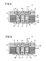
- FIG. 2 shows a top plan view of the thus formed light shielding block 7 with the eight unit plates P being stacked on each other
- FIG. 3 and FIG. 4 show vertical cross-sectional views along line III-III and line IV-IV of FIG. 2 , respectively, showing, in addition to the light shielding block 7, the lens holder 5 and the photodetector array 6 in the compound-eye imaging device 1.
- FIG. 3 and FIG. 4 show the horizontal position of the boundary h of each light-passing area as seen in the vertical cross-sectional view.
- Each of the light-passing holes H formed by stacking the unit plates P has an inner wall surface Ha that is an irregular or uneven surface as shown in FIG. 3 and FIG.
- FIG. 1 a process of assembling, into the compound-eye imaging device 1, of the lens holder 5, the light shielding block 7, the spacer frame 8 and the flexible board 13 with the photodetector array 6 mounted thereon will be described with reference to the above drawings, particularly FIG. 1 .
- the flexible board 13, the spacer frame 8, the light shielding block 7 and the lens holder 5 are inserted in this order into positioning pins 100 which are separately prepared.
- the light shielding block 7 is formed of total 8 (eight) stacked unit plates P in the above-described manner in advance.
- the flexible board 13, the spacer frame 8, the light shielding block 7 and the lens holder 5 are thus positioned by being inserted in the positioning pins 100 so as to allow lights emitted from the optical lenses 2 to form an image accurately on the photodetector array 6 through the respective light-passing holes H. If, at this time, the light shielding block 7 has a height (thickness) which is too large or too small relative to the focal length of each optical lens 2, the height can be easily adjusted by increasing or decreasing the number of unit plates P to form the light shielding block 7.
- the compound-eye imaging device 1 only requires one kind (one shape) of unit plates P, and thus can reduce the manufacturing cost as compared to that in which multiple kinds (multiple shapes) of unit plates are prepared.
- FIG. 6 is a schematic plan view of a light shielding block 7 used in a compound-eye imaging device 1 according to the second embodiment.
- FIG. 7A and FIG. 7B are schematic plan views of a first unit plate P1 and a second unit plate P2, respectively, to form the light shielding block 7.
- FIG. 8 is a schematic vertical cross-sectional view of the compound-eye imaging device 1 along line VIII-VIII of FIG. 6 , showing, in addition to the light shielding block 7, a lens holder 5 and a photodetector array 6 in the compound-eye imaging device 1.
- the compound-eye imaging device 1 of the second embodiment is similar to that of the first embodiment, except that the light shielding block 7 here is formed of two kinds of unit plates P1, P2 stacked on each other which are different from each other in shape.
- the other elements of the compound-eye imaging device 1 of the present embodiment are designated by the same reference numerals as the first embodiment, and the description thereof is omitted.
- the light shielding block 7 of the second embodiment is formed of two kinds of unit plates, first unit plates P1 and second unit plates P2, alternately stacked on each other. More specifically, the first unit plate P1 has relatively large rectangular light-passing windows W1 as shown in FIG. 7A , while the second unit plate P2 has relatively small rectangular light-passing windows W2, so as to form light-passing windows (W1, W2) having alternately different sizes, although both first and second unit plates P1, P2 have the same external shape and size. Furthermore, the light-passing windows W1, W2 of the first and second unit plates P1, P2 have the same center position (in each light-passing hole H) and similar shapes with different sizes.
- the light shielding block 7 is formed by alternately stacking the two kinds of unit plates P1, P2.
- a second unit plate P2 shown in FIG. 7B is first placed at the bottom, and a first unit plate P1 shown in FIG 7A is placed thereon.
- a second and a first unit plates P2, P1 are again placed in a second sequence.
- second and first unit plates P2, P1 are alternately and repeatedly stacked in four sequences in total, thereby forming a stack of eight unit plates (four each of the second and first unit plates) P2, P1.
- FIG. 6 shows the thus formed light shielding block 7 as seen in plan view, having a stack of total eight unit plates P1, P2, while FIG. 8 shows the vertical cross-sectional view of the light shielding block 7 along line VIII-VIII of FIG. 6 together with the lens holder 5 and the photodetector array 6 in the compound-eye imaging device 1.
- Each of the light-passing holes H formed by stacking the two kinds of unit plates P1, P2 has an inner wall surface Ha that is an irregular or uneven surface as shown in FIG. 8 , which irregularly reflects and scatters light such as shown by a long arrow A in FIG. 8 among lights emitted from the optical lenses 2 and directed toward the photodetector array 6. This light scattering or irregular reflection makes it possible to prevent ghost (ghost image) and flare from being produced in an image formed by the photodetector array 6.
- a feature of the second embodiment in contrast to the first embodiment, is that the effective light-passing areas of the light-passing holes H (windows W1, W2) are not required to be symmetrically left and right with respect to the longitudinal center line and symmetrically up and down with respect to the lateral center line in each unit plate.
- the concept of the second embodiment can work even if the light-passing holes H or their effective light-passing areas are displaced or offset from the center of each of the unit plates P1, P2.
- the use of only one kind of unit plates as in the first embodiment does not work, if it is required to make such light shielding block 7 having light-passing holes displaced or offset from the center of each unit plate as shown e.g. in FIG 6 .
- FIG. 9 is a schematic vertical cross-sectional view, corresponding to the vertical cross-sectional view of FIG. 3, FIG. 4 and FIG. 8 , of a compound-eye imaging device 1 according to the third embodiment.
- a feature of the compound-eye imaging device 1 of the present embodiment is that, as shown in FIG. 9 , each of the unit plates P has a tapered surface on an inner wall surface Wa in each of the light-passing windows W therein so as to form an irregular or uneven inner wall surface Ha, which serves as a light scattering surface, in each of the light-passing holes H of the light shielding block 7.
- the compound-eye imaging device 1 of the present embodiment is similar to that of the first or the second embodiment.
- the other elements of the compound-eye imaging device 1 of the present embodiment are designated by the same reference numerals as the first and second embodiments, and the description thereof is omitted.
- the tapered surface on each inner wall surface Wa can have any appropriate shape.
- a typical example of the shape of the tapered surface is such that the cross section of the tapered surface in a plane, which is parallel to the optical axis L and perpendicular to the inner wall surface Wa or the side of the light-passing window W, is a triangle with a base having a length equal to the thickness of the unit plate P and with an apex located away from the base.
- Each of the light-passing windows W formed in each unit plate P may have an appropriate size at an appropriate position.
- the sizes and the positions of the light-passing windows W in each unit plate P can be the same as those in the other unit plates P.
- the positions of the light-passing windows W in the respective unit plates P can be alternately offset (staggered). Furthermore, as in the second embodiment, the sizes of the light-passing windows W in the respective unit plates P can be different from one another.
- the tapered surface on each inner wall surface Wa can be formed by any appropriate process such as etching or drilling using a drill with a tapered bit.
- the inner wall surface Ha of each of the light-passing holes H is formed to have an irregular or uneven surface to serve as a light scattering surface.
- the inner wall surface Ha irregularly reflects and scatters light such as shown by a long arrow A in the drawings among lights emitted from the optical lenses 2 and directed toward the photodetector array 6, so that the inner wall surface Ha prevents the light from arriving at the photodetector array 6 to form ghost (ghost image) and flare in an image formed on the photodetector array 6.
Landscapes
- Engineering & Computer Science (AREA)
- Multimedia (AREA)
- Signal Processing (AREA)
- Physics & Mathematics (AREA)
- General Physics & Mathematics (AREA)
- Optics & Photonics (AREA)
- Optical Elements Other Than Lenses (AREA)
- Cameras In General (AREA)
- Lens Barrels (AREA)
- Transforming Light Signals Into Electric Signals (AREA)
- Studio Devices (AREA)
Claims (4)
- Dispositif de prise de vues de type oeil à facettes, comprenant :un réseau de lentilles optiques (4) avec plusieurs lentilles optiques intégrées (2) ;un élément d'arrêt (11) pour empêcher la lumière ambiante non nécessaire d'entrer dans les lentilles optiques (2) ;un réseau photodétecteur (6) qui est placé à une distance prédéterminée du réseau de lentilles optiques (4) pour reproduire des images formées par les lentilles optiques (2), respectivement ; etun bloc pare-lumière (7) qui est placé entre le réseau de lentilles optiques (4) et le réseau photodétecteur (6) pour diviser un espace situé entre ledit réseau de lentilles optiques (4) et ledit réseau photodétecteur (6) en une matrice d'espaces, avec des trous laissant passer la lumière (H), vu sur un plan perpendiculaire à l'axe optique de chaque lentille optique (2), de manière à empêcher une interférence entre les lumières émises à partir des lentilles optiques (2),caractérisé en ce que le bloc pare-lumière (7) se compose d'un empilement de plusieurs plaques unitaires (P) sur lesquelles sont prévues plusieurs fenêtres laissant passer la lumière (W), au niveau de positions horizontales correspondant aux positions horizontales des lentilles optiques (2), pour laisser passer les lumières émises à partir de celles-ci, de manière à former les trous laissant passer la lumière (H), respectivement,et en ce que chacun des trous laissant passer la lumière (H) formés par les fenêtres laissant passer la lumière (W) des plaques unitaires (P) prévues dans l'empilement a une surface de paroi intérieure irrégulière (Ha) qui sert de surface de diffusion de la lumière.
- Dispositif de prise de vues de type oeil à facettes selon la revendication 1,
dans lequel chacune des fenêtres laissant passer la lumière (W) de chacune des plaques unitaires (P) a une surface noircie, et
dans lequel les plaques unitaires (P) de l'empilement sont en alternance tournées sens dessus dessous et de gauche à droite de manière à permettre aux positions horizontales des fenêtres laissant passer la lumière (W), prévues pour former chaque trou laissant passer la lumière (H) à travers les plaques unitaires (P) de l'empilement, d'être décalées en alternance dans le sens de la profondeur du trou laissant passer la lumière (H), formant ainsi la surface de paroi intérieure irrégulière (Ha). - Dispositif de prise de vues de type oeil à facettes selon la revendication 1,
dans lequel chacune des fenêtres laissant passer la lumière (W) de chacune des plaques unitaires (P) a une surface noircie, et
dans lequel les fenêtres laissant passer la lumière (W) des plaques unitaires (P) de l'empilement ont en alternance des tailles différentes de manière à permettre aux positions horizontales desdites fenêtres laissant passer la lumière (W), prévues pour former chaque trou laissant passer la lumière (H) à travers les plaques unitaires (P) de l'empilement, d'être décalées en alternance dans le sens de la profondeur du trou laissant passer la lumière (H), formant ainsi la surface de paroi intérieure irrégulière (Ha). - Dispositif de prise de vues de type oeil à facettes selon la revendication 1, dans lequel chacune des plaques unitaires (P) a une surface effilée sur la surface de paroi intérieure (Wa) dans chacune des fenêtres laissant passer la lumière (W), de manière à permettre à chaque trou laissant passer la lumière (H) à travers les plaques unitaires (P) de l'empilement d'avoir ladite surface de paroi intérieure irrégulière (Ha).
Applications Claiming Priority (1)
| Application Number | Priority Date | Filing Date | Title |
|---|---|---|---|
| JP2006159503A JP2007329714A (ja) | 2006-06-08 | 2006-06-08 | 複眼撮像装置 |
Publications (3)
| Publication Number | Publication Date |
|---|---|
| EP1865713A2 EP1865713A2 (fr) | 2007-12-12 |
| EP1865713A3 EP1865713A3 (fr) | 2009-04-08 |
| EP1865713B1 true EP1865713B1 (fr) | 2010-09-15 |
Family
ID=38512552
Family Applications (1)
| Application Number | Title | Priority Date | Filing Date |
|---|---|---|---|
| EP07011279A Not-in-force EP1865713B1 (fr) | 2006-06-08 | 2007-06-08 | Dispositif de prise de vues de type oeil à facettes |
Country Status (4)
| Country | Link |
|---|---|
| US (1) | US7453056B2 (fr) |
| EP (1) | EP1865713B1 (fr) |
| JP (1) | JP2007329714A (fr) |
| DE (1) | DE602007009158D1 (fr) |
Families Citing this family (27)
| Publication number | Priority date | Publication date | Assignee | Title |
|---|---|---|---|---|
| WO2007083579A1 (fr) * | 2006-01-20 | 2007-07-26 | Matsushita Electric Industrial Co., Ltd. | Module de caméra oculaire composite et procédé de production de celui-ci |
| TWI505703B (zh) | 2007-12-19 | 2015-10-21 | 新加坡恒立私人有限公司 | 光學模組,晶圓等級的封裝及其製造方法 |
| WO2009104394A1 (fr) * | 2008-02-18 | 2009-08-27 | パナソニック株式会社 | Module d'appareil photo à œil composé |
| US8259223B2 (en) * | 2008-03-26 | 2012-09-04 | Kyocera Corporation | Imaging module |
| JP5155019B2 (ja) * | 2008-05-30 | 2013-02-27 | オリンパスメディカルシステムズ株式会社 | 絞り一体型間隔環及び絞り一体型レンズ枠 |
| JP5610254B2 (ja) * | 2008-06-18 | 2014-10-22 | 株式会社リコー | 撮像装置及び路面状態判別方法 |
| JP5448685B2 (ja) * | 2009-09-30 | 2014-03-19 | 富士フイルム株式会社 | 素子アレイ、素子アレイ積層体、及び素子アレイ積層体の製造方法 |
| JP2011128355A (ja) * | 2009-12-17 | 2011-06-30 | Sony Corp | 撮像レンズ及び撮像レンズを用いたカメラモジュール並びに撮像レンズの製造方法及びカメラモジュールの製造方法 |
| CN102081296B (zh) * | 2010-12-01 | 2012-11-07 | 南京航空航天大学 | 仿复眼视觉动目标快速定位及全景图同步获取装置及方法 |
| JP6071206B2 (ja) * | 2012-02-09 | 2017-02-01 | キヤノン株式会社 | 照明システム |
| CN103685881B (zh) * | 2012-09-19 | 2018-09-21 | Lg伊诺特有限公司 | 照相机模块 |
| JP6380391B2 (ja) * | 2013-05-31 | 2018-08-29 | コニカミノルタ株式会社 | 積層型レンズアレイユニット及び撮像装置 |
| JPWO2014199765A1 (ja) * | 2013-06-10 | 2017-02-23 | コニカミノルタ株式会社 | 複眼撮像装置 |
| WO2014203675A1 (fr) * | 2013-06-17 | 2014-12-24 | コニカミノルタ株式会社 | Système optique d'imagerie à œil à facettes et dispositif d'imagerie à œil à facettes |
| JP2015099262A (ja) * | 2013-11-19 | 2015-05-28 | ソニー株式会社 | 固体撮像装置およびカメラモジュール、並びに電子機器 |
| JPWO2016208403A1 (ja) * | 2015-06-23 | 2018-04-12 | ソニー株式会社 | イメージセンサ、および電子機器 |
| JP6499042B2 (ja) * | 2015-08-20 | 2019-04-10 | 京セラ株式会社 | 撮像素子実装用基板および撮像装置 |
| KR102604023B1 (ko) * | 2016-03-10 | 2023-11-20 | 삼성디스플레이 주식회사 | 광산란 필름 및 이를 포함하는 표시장치 |
| JP6750862B2 (ja) * | 2016-07-13 | 2020-09-02 | キヤノン株式会社 | 撮像素子およびその実装基板 |
| US20200359915A1 (en) * | 2018-01-15 | 2020-11-19 | Sony Corporation | Biological information obtaining device, biological information obtaining method, and wearable device |
| CN110650269A (zh) * | 2018-06-27 | 2020-01-03 | 三赢科技(深圳)有限公司 | 相机模组及其形成方法 |
| CN108759578B (zh) * | 2018-07-11 | 2023-09-01 | 速得尔科技(北京)有限公司 | 一种指向性光路保护装置和抗光干扰光幕电子靶系统 |
| JP2020086224A (ja) * | 2018-11-28 | 2020-06-04 | 株式会社アサヒ電子研究所 | 複眼撮像装置および複眼光学系 |
| JP7293791B2 (ja) * | 2019-03-26 | 2023-06-20 | 富士フイルムビジネスイノベーション株式会社 | 光学装置、画像読取装置、および画像形成装置 |
| JP7341838B2 (ja) * | 2019-10-10 | 2023-09-11 | 株式会社アサヒ電子研究所 | 複眼撮像装置および複眼撮像装置の製造方法 |
| CN114545607B (zh) * | 2022-01-26 | 2023-04-07 | 北京理工大学 | 一种微型超近距离大景深复眼成像系统 |
| CN115356792B (zh) * | 2022-06-27 | 2023-12-08 | 杭州海康微影传感科技有限公司 | 光学镜头晶圆的制作方法与镜头成像模组的制作方法 |
Family Cites Families (14)
| Publication number | Priority date | Publication date | Assignee | Title |
|---|---|---|---|---|
| US4663738A (en) * | 1984-12-04 | 1987-05-05 | Xerox Corporation | High density block oriented solid state optical memories |
| JPH05183135A (ja) * | 1991-10-14 | 1993-07-23 | Sony Corp | Ccd撮像装置 |
| US5514888A (en) * | 1992-05-22 | 1996-05-07 | Matsushita Electronics Corp. | On-chip screen type solid state image sensor and manufacturing method thereof |
| US5751492A (en) | 1996-06-14 | 1998-05-12 | Eastman Kodak Company | Diffractive/Refractive lenslet array incorporating a second aspheric surface |
| JPH10253920A (ja) | 1997-03-12 | 1998-09-25 | Fujitsu Ltd | 光学装置 |
| JPH11231109A (ja) * | 1998-02-16 | 1999-08-27 | Kyocera Corp | 遮光板及びその製造方法 |
| JP3821614B2 (ja) | 1999-08-20 | 2006-09-13 | 独立行政法人科学技術振興機構 | 画像入力装置 |
| US6646807B2 (en) * | 2001-06-19 | 2003-11-11 | Rohm Co., Ltd. | Lens array unit and process for making lens array |
| JP2003143459A (ja) * | 2001-11-02 | 2003-05-16 | Canon Inc | 複眼撮像系およびこれを備えた装置 |
| US6939015B2 (en) * | 2002-09-20 | 2005-09-06 | Eastman Kodak Company | Chromium black light shield |
| JP3959041B2 (ja) | 2003-03-27 | 2007-08-15 | 独立行政法人科学技術振興機構 | 撮像装置及び輝度分布測定装置 |
| US7227692B2 (en) * | 2003-10-09 | 2007-06-05 | Micron Technology, Inc | Method and apparatus for balancing color response of imagers |
| JP2005156989A (ja) * | 2003-11-26 | 2005-06-16 | Olympus Corp | 鏡枠 |
| DE102004003013B3 (de) * | 2004-01-20 | 2005-06-02 | Fraunhofer-Gesellschaft zur Förderung der angewandten Forschung e.V. | Bilderfassungssystem und dessen Verwendung |
-
2006
- 2006-06-08 JP JP2006159503A patent/JP2007329714A/ja not_active Ceased
-
2007
- 2007-06-07 US US11/759,566 patent/US7453056B2/en not_active Expired - Fee Related
- 2007-06-08 DE DE602007009158T patent/DE602007009158D1/de active Active
- 2007-06-08 EP EP07011279A patent/EP1865713B1/fr not_active Not-in-force
Also Published As
| Publication number | Publication date |
|---|---|
| US20070284511A1 (en) | 2007-12-13 |
| DE602007009158D1 (de) | 2010-10-28 |
| EP1865713A2 (fr) | 2007-12-12 |
| US7453056B2 (en) | 2008-11-18 |
| EP1865713A3 (fr) | 2009-04-08 |
| JP2007329714A (ja) | 2007-12-20 |
Similar Documents
| Publication | Publication Date | Title |
|---|---|---|
| EP1865713B1 (fr) | Dispositif de prise de vues de type oeil à facettes | |
| US7525081B2 (en) | Compound-eye imaging device having a light shielding block with a stack of multiple flat unit plates | |
| US8237841B2 (en) | Compound-eye imaging device | |
| JP4950103B2 (ja) | 正立等倍レンズアレイプレート、イメージセンサユニットおよび画像読取装置 | |
| US20150036219A1 (en) | Lens array module | |
| AU2020226426B2 (en) | Screen assembly and electronic device | |
| KR20110017278A (ko) | 웨이퍼-레벨 렌즈 모듈 및 이를 구비하는 촬상 장치 | |
| TW201416701A (zh) | 光學裝置,尤其是運算式相機,及其製造方法 | |
| US9097878B2 (en) | Image capture module | |
| KR101931402B1 (ko) | 마이크로 렌즈 어레이 및 그것을 사용한 스캔 노광 장치 | |
| JPS59143467A (ja) | 全巾走査アレーを製造する装置および方法 | |
| CN101459165A (zh) | 电子元件晶片模块、其制造方法以及电子信息设备 | |
| CN100466679C (zh) | 图像传感器 | |
| JPH10301143A (ja) | 液晶表示装置のアライメントマーク | |
| JPH03175403A (ja) | 固体撮像装置 | |
| US10110788B2 (en) | Camera device | |
| JPH1141410A (ja) | 光学装置 | |
| US12320962B2 (en) | Optical elements and wafers including optical elements | |
| JP4843515B2 (ja) | 半導体チップの積層構造 | |
| CN104917937A (zh) | 影像撷取组件及其镜头单元阵列 | |
| JP2008292172A (ja) | 傾斜センサ | |
| JP4064579B2 (ja) | 赤外線データ通信モジュールの製造方法 | |
| CN106133919A (zh) | 晶元级光学组件及其制造方法 | |
| KR101288281B1 (ko) | 렌즈 모듈 및 그 제조방법 | |
| US9083872B2 (en) | Imaging device with adhesive filling openings and related methods |
Legal Events
| Date | Code | Title | Description |
|---|---|---|---|
| PUAI | Public reference made under article 153(3) epc to a published international application that has entered the european phase |
Free format text: ORIGINAL CODE: 0009012 |
|
| AK | Designated contracting states |
Kind code of ref document: A2 Designated state(s): AT BE BG CH CY CZ DE DK EE ES FI FR GB GR HU IE IS IT LI LT LU LV MC MT NL PL PT RO SE SI SK TR |
|
| AX | Request for extension of the european patent |
Extension state: AL BA HR MK YU |
|
| PUAL | Search report despatched |
Free format text: ORIGINAL CODE: 0009013 |
|
| AK | Designated contracting states |
Kind code of ref document: A3 Designated state(s): AT BE BG CH CY CZ DE DK EE ES FI FR GB GR HU IE IS IT LI LT LU LV MC MT NL PL PT RO SE SI SK TR |
|
| AX | Request for extension of the european patent |
Extension state: AL BA HR MK RS |
|
| 17P | Request for examination filed |
Effective date: 20090722 |
|
| AKX | Designation fees paid |
Designated state(s): DE FR GB |
|
| GRAP | Despatch of communication of intention to grant a patent |
Free format text: ORIGINAL CODE: EPIDOSNIGR1 |
|
| GRAS | Grant fee paid |
Free format text: ORIGINAL CODE: EPIDOSNIGR3 |
|
| GRAA | (expected) grant |
Free format text: ORIGINAL CODE: 0009210 |
|
| AK | Designated contracting states |
Kind code of ref document: B1 Designated state(s): DE FR GB |
|
| REG | Reference to a national code |
Ref country code: GB Ref legal event code: FG4D |
|
| REF | Corresponds to: |
Ref document number: 602007009158 Country of ref document: DE Date of ref document: 20101028 Kind code of ref document: P |
|
| PLBE | No opposition filed within time limit |
Free format text: ORIGINAL CODE: 0009261 |
|
| STAA | Information on the status of an ep patent application or granted ep patent |
Free format text: STATUS: NO OPPOSITION FILED WITHIN TIME LIMIT |
|
| 26N | No opposition filed |
Effective date: 20110616 |
|
| REG | Reference to a national code |
Ref country code: DE Ref legal event code: R097 Ref document number: 602007009158 Country of ref document: DE Effective date: 20110616 |
|
| REG | Reference to a national code |
Ref country code: FR Ref legal event code: PLFP Year of fee payment: 9 |
|
| PGFP | Annual fee paid to national office [announced via postgrant information from national office to epo] |
Ref country code: GB Payment date: 20150603 Year of fee payment: 9 Ref country code: DE Payment date: 20150602 Year of fee payment: 9 |
|
| PGFP | Annual fee paid to national office [announced via postgrant information from national office to epo] |
Ref country code: FR Payment date: 20150608 Year of fee payment: 9 |
|
| REG | Reference to a national code |
Ref country code: DE Ref legal event code: R119 Ref document number: 602007009158 Country of ref document: DE |
|
| GBPC | Gb: european patent ceased through non-payment of renewal fee |
Effective date: 20160608 |
|
| REG | Reference to a national code |
Ref country code: FR Ref legal event code: ST Effective date: 20170228 |
|
| PG25 | Lapsed in a contracting state [announced via postgrant information from national office to epo] |
Ref country code: FR Free format text: LAPSE BECAUSE OF NON-PAYMENT OF DUE FEES Effective date: 20160630 Ref country code: DE Free format text: LAPSE BECAUSE OF NON-PAYMENT OF DUE FEES Effective date: 20170103 |
|
| PG25 | Lapsed in a contracting state [announced via postgrant information from national office to epo] |
Ref country code: GB Free format text: LAPSE BECAUSE OF NON-PAYMENT OF DUE FEES Effective date: 20160608 |