EP1845554A2 - Verfahren zur Erzeugung von supersekundärem Kornwachstum in schmalen Gräben - Google Patents
Verfahren zur Erzeugung von supersekundärem Kornwachstum in schmalen Gräben Download PDFInfo
- Publication number
- EP1845554A2 EP1845554A2 EP06126251A EP06126251A EP1845554A2 EP 1845554 A2 EP1845554 A2 EP 1845554A2 EP 06126251 A EP06126251 A EP 06126251A EP 06126251 A EP06126251 A EP 06126251A EP 1845554 A2 EP1845554 A2 EP 1845554A2
- Authority
- EP
- European Patent Office
- Prior art keywords
- copper
- ecd
- barrier layer
- pvd
- layer
- Prior art date
- Legal status (The legal status is an assumption and is not a legal conclusion. Google has not performed a legal analysis and makes no representation as to the accuracy of the status listed.)
- Withdrawn
Links
Images




Classifications
-
- H—ELECTRICITY
- H10—SEMICONDUCTOR DEVICES; ELECTRIC SOLID-STATE DEVICES NOT OTHERWISE PROVIDED FOR
- H10W—GENERIC PACKAGES, INTERCONNECTIONS, CONNECTORS OR OTHER CONSTRUCTIONAL DETAILS OF DEVICES COVERED BY CLASS H10
- H10W20/00—Interconnections in chips, wafers or substrates
- H10W20/01—Manufacture or treatment
- H10W20/031—Manufacture or treatment of conductive parts of the interconnections
- H10W20/056—Manufacture or treatment of conductive parts of the interconnections by filling conductive material into holes, grooves or trenches
-
- H—ELECTRICITY
- H10—SEMICONDUCTOR DEVICES; ELECTRIC SOLID-STATE DEVICES NOT OTHERWISE PROVIDED FOR
- H10P—GENERIC PROCESSES OR APPARATUS FOR THE MANUFACTURE OR TREATMENT OF DEVICES COVERED BY CLASS H10
- H10P14/00—Formation of materials, e.g. in the shape of layers or pillars
- H10P14/40—Formation of materials, e.g. in the shape of layers or pillars of conductive or resistive materials
- H10P14/412—Deposition of metallic or metal-silicide materials
-
- H—ELECTRICITY
- H10—SEMICONDUCTOR DEVICES; ELECTRIC SOLID-STATE DEVICES NOT OTHERWISE PROVIDED FOR
- H10P—GENERIC PROCESSES OR APPARATUS FOR THE MANUFACTURE OR TREATMENT OF DEVICES COVERED BY CLASS H10
- H10P14/00—Formation of materials, e.g. in the shape of layers or pillars
- H10P14/40—Formation of materials, e.g. in the shape of layers or pillars of conductive or resistive materials
- H10P14/42—Formation of materials, e.g. in the shape of layers or pillars of conductive or resistive materials using a gas or vapour
- H10P14/44—Physical vapour deposition [PVD]
-
- H—ELECTRICITY
- H10—SEMICONDUCTOR DEVICES; ELECTRIC SOLID-STATE DEVICES NOT OTHERWISE PROVIDED FOR
- H10P—GENERIC PROCESSES OR APPARATUS FOR THE MANUFACTURE OR TREATMENT OF DEVICES COVERED BY CLASS H10
- H10P14/00—Formation of materials, e.g. in the shape of layers or pillars
- H10P14/40—Formation of materials, e.g. in the shape of layers or pillars of conductive or resistive materials
- H10P14/46—Formation of materials, e.g. in the shape of layers or pillars of conductive or resistive materials using a liquid
- H10P14/47—Electrolytic deposition, i.e. electroplating; Electroless plating
-
- H—ELECTRICITY
- H10—SEMICONDUCTOR DEVICES; ELECTRIC SOLID-STATE DEVICES NOT OTHERWISE PROVIDED FOR
- H10W—GENERIC PACKAGES, INTERCONNECTIONS, CONNECTORS OR OTHER CONSTRUCTIONAL DETAILS OF DEVICES COVERED BY CLASS H10
- H10W20/00—Interconnections in chips, wafers or substrates
- H10W20/01—Manufacture or treatment
- H10W20/031—Manufacture or treatment of conductive parts of the interconnections
- H10W20/032—Manufacture or treatment of conductive parts of the interconnections of conductive barrier, adhesion or liner layers
- H10W20/033—Manufacture or treatment of conductive parts of the interconnections of conductive barrier, adhesion or liner layers in openings in dielectrics
-
- H—ELECTRICITY
- H10—SEMICONDUCTOR DEVICES; ELECTRIC SOLID-STATE DEVICES NOT OTHERWISE PROVIDED FOR
- H10W—GENERIC PACKAGES, INTERCONNECTIONS, CONNECTORS OR OTHER CONSTRUCTIONAL DETAILS OF DEVICES COVERED BY CLASS H10
- H10W20/00—Interconnections in chips, wafers or substrates
- H10W20/01—Manufacture or treatment
- H10W20/031—Manufacture or treatment of conductive parts of the interconnections
- H10W20/032—Manufacture or treatment of conductive parts of the interconnections of conductive barrier, adhesion or liner layers
- H10W20/055—Manufacture or treatment of conductive parts of the interconnections of conductive barrier, adhesion or liner layers by formation methods other than physical vapour deposition [PVD], chemical vapour deposition [CVD] or liquid deposition
-
- H—ELECTRICITY
- H10—SEMICONDUCTOR DEVICES; ELECTRIC SOLID-STATE DEVICES NOT OTHERWISE PROVIDED FOR
- H10W—GENERIC PACKAGES, INTERCONNECTIONS, CONNECTORS OR OTHER CONSTRUCTIONAL DETAILS OF DEVICES COVERED BY CLASS H10
- H10W20/00—Interconnections in chips, wafers or substrates
- H10W20/01—Manufacture or treatment
- H10W20/031—Manufacture or treatment of conductive parts of the interconnections
- H10W20/032—Manufacture or treatment of conductive parts of the interconnections of conductive barrier, adhesion or liner layers
- H10W20/055—Manufacture or treatment of conductive parts of the interconnections of conductive barrier, adhesion or liner layers by formation methods other than physical vapour deposition [PVD], chemical vapour deposition [CVD] or liquid deposition
- H10W20/0552—Manufacture or treatment of conductive parts of the interconnections of conductive barrier, adhesion or liner layers by formation methods other than physical vapour deposition [PVD], chemical vapour deposition [CVD] or liquid deposition by diffusing metallic dopants to react with dielectrics
-
- H—ELECTRICITY
- H10—SEMICONDUCTOR DEVICES; ELECTRIC SOLID-STATE DEVICES NOT OTHERWISE PROVIDED FOR
- H10W—GENERIC PACKAGES, INTERCONNECTIONS, CONNECTORS OR OTHER CONSTRUCTIONAL DETAILS OF DEVICES COVERED BY CLASS H10
- H10W20/00—Interconnections in chips, wafers or substrates
- H10W20/01—Manufacture or treatment
- H10W20/031—Manufacture or treatment of conductive parts of the interconnections
- H10W20/064—Manufacture or treatment of conductive parts of the interconnections by modifying the conductivity of conductive parts, e.g. by alloying
-
- H—ELECTRICITY
- H10—SEMICONDUCTOR DEVICES; ELECTRIC SOLID-STATE DEVICES NOT OTHERWISE PROVIDED FOR
- H10W—GENERIC PACKAGES, INTERCONNECTIONS, CONNECTORS OR OTHER CONSTRUCTIONAL DETAILS OF DEVICES COVERED BY CLASS H10
- H10W20/00—Interconnections in chips, wafers or substrates
- H10W20/40—Interconnections external to wafers or substrates, e.g. back-end-of-line [BEOL] metallisations or vias connecting to gate electrodes
- H10W20/41—Interconnections external to wafers or substrates, e.g. back-end-of-line [BEOL] metallisations or vias connecting to gate electrodes characterised by their conductive parts
- H10W20/425—Barrier, adhesion or liner layers
-
- H—ELECTRICITY
- H10—SEMICONDUCTOR DEVICES; ELECTRIC SOLID-STATE DEVICES NOT OTHERWISE PROVIDED FOR
- H10W—GENERIC PACKAGES, INTERCONNECTIONS, CONNECTORS OR OTHER CONSTRUCTIONAL DETAILS OF DEVICES COVERED BY CLASS H10
- H10W20/00—Interconnections in chips, wafers or substrates
- H10W20/40—Interconnections external to wafers or substrates, e.g. back-end-of-line [BEOL] metallisations or vias connecting to gate electrodes
- H10W20/41—Interconnections external to wafers or substrates, e.g. back-end-of-line [BEOL] metallisations or vias connecting to gate electrodes characterised by their conductive parts
- H10W20/44—Conductive materials thereof
- H10W20/4403—Conductive materials thereof based on metals, e.g. alloys, metal silicides
- H10W20/4421—Conductive materials thereof based on metals, e.g. alloys, metal silicides the principal metal being copper
Definitions
- the present invention is related to the field of semiconductor processing.
- Interconnects have been, are, and will continue to be a limiting factor for the performance and cost of integrated circuits. As technology scales down further, the problems associated with interconnects become ever more pressing. The introduction of low-resistive copper as an alternative interconnect material for aluminum presents researchers with some new challenges, since copper cannot be implemented in the same manner as aluminum alloys.
- PVD Physical Vapor Deposition
- sputter deposition has long time been one of the techniques of choice for metallization in integrated circuits.
- sputter deposition has been widely used in the manufacturing of high-performance on-chip interconnect.
- Sputtering techniques are however widely used to deposit a thin layer of diffusion barrier and/or seed layer in said features.
- PVD suffers from shadowing effects if the aspect ratio of features to be filled is sufficiently large. Said shadowing effects can form overhanging structures at the top corners of the trenches and vias. These effects can lead to void formation when attempting to fill a feature. Due to the geometrical shadowing, the film is preferentially deposited on the top corners leading to a "void" within the trench or via.
- Electroplated (also referred to as electrochemically deposited or ECD) copper has therefore become the method of choice for filling narrow interconnect features in the back-end-of-line processing for microelectronics applications.
- ECD electrochemically deposited
- the influence of the PVD deposited seed layer becomes more important when its thickness is not scaled accordingly. This changes the grain growth dynamics in trenches as the volume fractions of ECD and PVD change significantly.
- copper lines are fabricated by patterning trenches into a dielectric layer with optical lithography.
- a barrier layer and Cu seed are deposited within the trenches, followed by electroplating in order to fill the structures.
- a Chemical mechanical polishing (CMP) step is used to remove excess copper and barrier material.
- a standard hot-plate anneal step (e.g. 30' at 250 °C) is introduced before CMP to enhance re-crystallization of copper in both seedlayer and plated copper.
- SSGG super-secondary-grain-growth
- the SSGG produces [100] oriented super grains of several tens of micrometers, less grain boundaries are obtained and hence the resistance in copper having these super grains is lower. This makes the application of SSGG in interconnect structures very attractive. There is however still a need to understand the growth mechanisms of said SSGG, and to have said SSGG lead to large grains in interconnect structures (e.g. trenches) in semiconductor devices. So far, only growth in thin films has been demonstrated because the required thickness needed to make SSGG possible is larger than typical trench dimensions.
- the present invention relates to a semiconductor device comprising at least one trench and/or at least one via filled with recrystallized electrochemically deposited copper (ECD-Cu), wherein at least 80%, 85%, 90%, 91%, or 92% of said recrystallized ECD-Cu consist of copper grains having a [100] orientation and dimensions of at least 10 micron.
- ECD-Cu electrochemically deposited copper
- At least 93%, 94%, 95%, 96%, or 97% of said recrystallized ECD-Cu consist of said copper grains having a [100] orientation and dimensions of at least 10 micron.
- said recrystallized ECD-Cu consist of said copper grains having a [100] orientation and dimensions of at least 10 micron.
- the dimensions of said copper grains with a [100] orientation are of at least 20 or 25 micrometers.
- the dimensions of said copper grains with a [100] orientation are of at least 50 micrometers.
- the dimensions of said copper grains with a [100] orientation are of at least 100 micrometers.
- said trench or trenches have a width of less than 200 nm in a semiconductor device according to the invention.
- said trench(es) has (have) an aspect ratio (or height to width ratio) higher than 1.
- a semiconductor device comprises a diffusion barrier layer (for preventing the copper diffusion into the layer underneath, more particularly for preventing the copper diffusion into the dielectric layer underneath) and said recrystallized ECD-Cu upon said diffusion barrier layer.
- said diffusion barrier layer has a thickness of less than 8 nm.
- said diffusion barrier layer is a layer comprising or consisting of tantalum (Ta), titanium (Ti), ruthenium (Ru), tungsten (W) and/or Manganese (Mn).
- Another object of the present invention relates to a method for filling at least one trench and/or at least one via with copper, comprising the steps of:
- said trench(es) has (have) a width comprised between 50 nm and 200 nm.
- said trench(es) has (have) an aspect ratio higher than 1.
- said opening before the PVD deposition of copper (or inducing layer), said opening can be filled with ECD-Cu partially, substantially or completely. Preferably, said opening is completely filled with ECD-Cu.
- said thermal treatment (also referred to as thermal anneal) is performed at a temperature higher than the relaxation temperature of copper. More particularly, said thermal treatment is performed at a temperature higher than 80°C.
- said thermal treatment is performed at a temperature comprised between (about) 100°C and (about) 420°C, more preferably comprised between (about) 100°C and (about) 400°C, more particularly can be performed at (about) 130°C, and even more preferably at about 200°C.
- a substrate bias of 250W is applied during said PVD deposition step for depositing said PVD-Cu.
- said thermal treatment is performed for at least 30 minutes, more preferably for at least 1 hour, and even more preferably for at least 1,5 hour.
- the thickness of the PVD-Cu layer (5) is comprised between 400 nm and 1000 nm, and more particularly is about 500 nm.
- said barrier layer can comprise or consist of tantalum (Ta), titanium (Ti), ruthenium (Ru), tungsten (W) and/or Manganese (Mn).
- said barrier layer comprises or consists of ⁇ -Ta, ⁇ -Ta or TaN.
- a method according to the invention can further comprise, before the step of depositing said ECD-Cu, the step of depositing a copper seedlayer onto said barrier layer, preferably by means of a Physical Vapor Deposition process.
- a method according to the present invention can further comprise, before the step of depositing said PVD-Cu, the step of removing the overburden of ECD-Cu and seedlayer, using said barrier layer as a stopping layer.
- Said removal step of said overburden of ECD-Cu and seedlayer can be performed by chemical mechanical polishing (CMP).
- CMP chemical mechanical polishing
- Mn can be incorporated into a copper seedlayer (the Mn being incorporated during the step of depositing said copper seedlayer by Physical Vapor Deposition), and said Mn-containing-seedlayer is then submitted to a thermal treatment that causes the movement of the Mn towards the dielectric material such that the Mn-containing-seedlayer can act as a barrier layer.
- the deposition of a barrier layer prior to the deposition of said Mn-containing-seedlayer becomes then needless.
- the overburden of ECD-Cu (if any) can be removed by a wet and/or dry etchback process.
- the overburden of PVD-Cu and the overburden of barrier layer can be removed by chemical mechanical polishing (CMP). Said removal can also be performed by dry and/or wet etchback.
- CMP chemical mechanical polishing
- Mn can be incorporated in said ECD-Cu for migrating, during said thermal treatment step (for recrystallization of both ECD-Cu and PVD-Cu), towards said dielectric layer, to act as barrier layer.
- the thickness of ECD-Cu, the thickness of PVD-Cu, and/or the substrate bias applied more than 80%, or more than 93%, and even more than 98% or 99% (all the values, integer or real number, between 80% and 99% being envisaged) of said recrystallized ECD-Cu can consist of copper grains with a [100] orientation having dimensions of at least 10 micron, of at least 20 or 25 micron or of at least 100 micron.
- a method according to the invention can be used in the framework of a damascene method or of a dual damascene method for forming an interconnect.
- Another object of the present invention relates to a semiconductor device obtainable by a method according to the invention.
- Figure 1 illustrates the formation of conductive structures (e.g. trenches) and subsequent filling and recrystallization of copper within the trenches according to state of the art techniques.
- conductive structures e.g. trenches
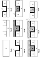
- FIGS 2A to 2I illustrate the preferred embodiment of the present invention for formation and filling of narrow trenches (or vias) with electroplated copper (ECD-Cu) and subsequent recrystallization of the copper according to the method of the invention to form (or to obtain) Super Secondary Grain Growth (SSGG) in said ECD-Cu.
- ECD-Cu electroplated copper
- SSGG Super Secondary Grain Growth
- Figures 3A to 3I illustrate an alternative and also preferred embodiment of the present invention for formation and filling of narrow trenches (or vias) using direct plating of copper onto a resistive barrier layer and subsequent recrystallization of the copper according to the method of the invention to form (or to obtain) Super Secondary Grain Growth (SSGG) in said ECD-Cu.
- SSGG Super Secondary Grain Growth
- FIGS 4A to 4H illustrate an alternative and also preferred embodiment of the present invention for formation and filling of narrow trenches (or vias) using electroplated copper.
- Said electroplated copper has a very thin overburden such that an extra planarizing step can be skipped. Subsequent recrystallization of the electroplated copper according to the method of the invention leads to Super Secondary Grain Growth (SSGG) in said ECD-Cu.
- SSGG Super Secondary Grain Growth
- Figure 6 illustrates the stress in ECD deposited copper as a function of the (annealing) temperature indicating the temperature range for growth of supergrains according to the method of the invention.
- Figure 7(a) illustrates the distribution of crystallographic orientations as observed in ECD deposited copper having the original [111] crystallographic orientation (texture).
- Figure 7(b) represents a grain structure where both SGG and SSGG grains are present. For the condition where SSGG is most complete as shown in Figure 7(c) the original [111] texture of the as-deposited film has disappeared completely (after performing the method of the invention).
- ECD Electrochemical Deposition
- ECP Electro Chemical Plating
- the ECD process is the process of depositing a metal (copper) by means of electrolysis and involves placing the wafer substrate in an aqueous electrolyte containing metal ions (e.g. Cu(II) ions).
- seed layer as referred to in this application is a layer used to provide a conductive path for the electric current that is required to electroplate copper.
- an underlying conductive seed layer is generally applied to the wafer before it is subjected to an electrochemical deposition process. PVD is the preferred application process for the conductive seed layer because it can readily deposit copper on the barrier layer with relatively good adhesion.
- direct plating refers to Electrochemical Deposition (ECD) or Electro Chemical Plating (ECP) using highly resistive barrier layers such that no seedlayer is needed and direct plating onto the barrier layer is possible.
- the orientation of the secondary grains and/or of the super secondary grains is expressed as a direction [xyz] parallel to the substrate.
- Super secondary grains have a [100] orientated growth while secondary grains have a [111] orientated growth.
- the term "aspect ratio” refers to the ratio of the height dimension to the width dimension of particular openings into which an electrical contact is to be placed.
- a via opening which typically extends in a tubular form through multiple layers has a height and a diameter
- the aspect ratio would be the height of the tubular divided by the diameter.
- the aspect ratio of a trench would be the height of the trench divided by the minimal travel width of the trench at its base.
- anneal refers to a heat treatment to which a wafer is subjected in order to modify properties of materials or structures processed on its surface or in the bulk.
- the present invention provides a method for creation of super secondary grains in narrow conductive structures such as trenches and vias in a semiconductor device.
- the method of the present invention is suitable for filling of an opening (a trench and/or a via) to form interconnect structure, e.g. a single damascene structure (SD) or a dual damascene structure (DD), with SSG.
- an opening e.g. a single damascene structure (SD) or a dual damascene structure (DD)
- SSG single damascene structure
- a method for filling trenches and/or vias for forming copper interconnect structures in a semiconductor device said copper being characterized as recrystallized electrochemically deposited copper and having enlarged copper grains with a [100] orientation.
- Said enlarged copper grains result from the recrystallization of ECD-Cu, said recrystallization of said ECD-Cu being induced by the recrystallization initiated into a PVD deposited copper layer (PVD-Cu) contacting and being situated on top of said ECD-Cu.
- PVD-Cu PVD deposited copper layer
- PVD-Cu PVD deposited copper layer
- the invention is based on the surprising discovery that the super secondary grains (SSG) after being induced in a PVD-Cu layer grow further into electrochemically filled copper trench, said electrochemically filled copper trench being situated underneath and in direct contact with said PVD-Cu layer. Indeed, said SSG cannot be obtained by annealing an ECD-Cu layer that is not into direct contact with a PVD-Cu layer.
- a method is disclosed to create (to allow) super secondary grain growth within narrow interconnect structures (trenches and/or vias) in semiconductor devices, said super secondary grains having a [100] oriented structure and a length of several tens of microns; said interconnect structures being preferably part of a single or dual damascene structure.
- the method of the present invention provides processing steps to create narrow trenches and/or vias filled with low resistivity copper being characterized as having super secondary grains. Recrystallized ECD-Cu according to a method of the invention exhibits lower resistivity than ECD-Cu obtained by standard methods.
- the processing preferably starts with first etching an opening (trench or via) in a dielectric layer.
- Said dielectric layer can be any suitable material to be used as dielectric material in semiconductor processing.
- said dielectric layer is a low-k dielectric material (i.e. a dielectric material having a dielectric constant lower than that of SiO 2 ).
- said trench opening preferably has a width of less than 200 nm and an aspect ratio of more than unity.
- a copper diffusion barrier layer is deposited in said opening.
- Said barrier layer is preferably a thin tantalum (Ta) comprising layer deposited by Physical Vapor Deposition (PVD) or atomic layer deposition (ALD).
- PVD Physical Vapor Deposition
- ALD atomic layer deposition
- said Ta comprising barrier layer is a ⁇ -Ta, ⁇ -Ta or TaN comprising layer.
- Said barrier layer can be a ⁇ -Ta, ⁇ -Ta or TaN layer.
- the barrier layer has preferably a thickness of less than 8 nm and more preferred has a thickness of less than 10% of the trench width.
- a thin copper seedlayer can be deposited, said seedlayer is preferably deposited by PVD.
- Direct plating can also be performed, for which there is no need to deposit a copper seedlayer onto the barrier layer.
- Direct plating uses highly resistive barrier layers such that no seedlayer is needed and direct plating onto the barrier layer is possible.
- ECD-Cu electrochemically plated copper
- the overburden of ECD-Cu and (optionally) of PVD-Cu seedlayer (if any) can be removed (from the field area) using the barrier layer (on the field) as a stopping layer.
- the removal process is preferably a chemical mechanical polishing step. Alternatively a wet or dry etchback process can be used.
- a second thick copper layer (preferably thicker than the ECD-Cu layer), further referred to as inducing layer is deposited onto the planarized surface by Physical Vapor Deposition (PVD-Cu) using a high bias.
- PVD-Cu Physical Vapor Deposition
- Said high bias is preferably higher than 150 W. More preferred said bias is at least 250W for a 200mm wafer. The optimal bias setting for a 300 mm wafer is thus higher.
- the thickness of said second PVD-Cu layer or inducing layer is preferably in the range of 400nm to 1000nm and most preferred 500nm.
- a thermal anneal is performed to induce super secondary grain growth in the thick PVD-Cu inducing layer. Then said super secondary grains further "migrate” (or grow, or expand) further into the ECD-Cu such that lower resistivity copper having super secondary grains (SSG) is obtained.
- SSG super secondary grains
- the expansion process has to be understood as a process during which the induced SSG keep on growing such that they grow further into the narrow structures filled with ECD-Cu, such that said SSG substantially fill said narrow structures.
- the thermal anneal is performed at temperatures above the relaxation temperature of copper.
- Said relaxation temperature is about 80°C.
- Said thermal anneal can be performed at temperatures in the range of 80°C up to 120°C.
- said thermal anneal is performed at temperatures in the range of 100°C up to 420°C, more preferably in the range of 100°C up to 400°C and even more preferably around 200°C.
- the overburden of the second PVD-Cu inducing layer is removed.
- the removal is preferably performed by chemical mechanical polishing (CMP) or alternatively by a wet and/or dry etchback process.
- CMP chemical mechanical polishing
- the barrier layer on the field can be removed subsequently to the removal of the inducing layer.
- the PVD copper inducing layer can be deposited directly on top of this ECD layer without the intermediate CMP step. And the final CMP step removes the PVD inducing layer, barrier layer, seedlayer (if any) and ECD-Cu on the field.
- the barrier step can be skipped and a seedlayer comprising Mn can be deposited before ECD. This Mn solute then forms a barrier layer during the thermal anneal step.
- Mn can be incorporated in ECD-Cu during plating. Said Mn then migrates during a thermal anneal towards the dielectric and act there as a barrier.
- the present invention also relates to a semiconductor device having at least one interconnect structure filled with (recrystallized) electrochemically deposited copper (ECD-Cu), said ECD-Cu is further characterized as low resistivity copper and having super secondary copper grains (SSG). Said SSG have a [100] orientation.
- more than 80% of said recrystallized ECD copper are in the form of SSG with a [100] orientation.
- more than 93% of said recrystallized ECD copper are in the form of SSG with a [100] orientation.
- more than 98% of said recrystallized ECD copper are in the form of SSG with a [100] orientation.
- Said SSG are further characterized as having dimensions of at least 10 micron.
- said SSG have dimensions of at least 20 micron, of at least 25 micron, of at least 50 micron, and more preferably of at least 100 micron.
- Said SSG grains are first formed in a PVD-Cu inducing layer which is into contact with said ECD-Cu and said SSG grains "migrating” (or growing, or expanding) further in said ECD-Cu.
- the PVD-Cu layer is preferably removed after "migration” (or growth, or expansion) of the SSG into the ECD-Cu.
- Interconnect structures made of copper having enlarged copper grains have improved resistivity due to a decrease of the number of grain boundaries per unit volume.
- Said enlarged copper grains have preferably a dimension of at least 10 micron ( ⁇ m), more preferred more than 25 micron ( ⁇ m) and most preferred more than 100 micron ( ⁇ m), whereas the conventional secondary copper grains as obtained after an anneal of ECD-Cu have dimensions of 1-2 microns ( ⁇ m).
- the copper used in a method or a semiconductor device according to the invention preferably includes alloys of copper of the kind typically used in the semiconductor industry. More preferably, and according to preferred embodiments, a copper alloy comprising about 98% by weight of copper is used.
- a method of the invention solves the problem of filling trenches having aspect ratios greater than 1 for forming interconnect structures without voids and with low resistivity copper.
- PVD Physical Vapor Deposition
- ECD is known as a technique capable of perfect bottom-up fill of narrow features.
- stress in a PVD deposited copper can be tuned during the deposition process by tuning the substrate bias, leading to an excess (e.g. more than 80%) of the more preferred [100] orientation of the copper such that growth of super secondary copper grains (SSG) is possible.
- SSG super secondary copper grains
- the present invention combines the benefits of both techniques for filling trenches and/or vias for forming interconnect structures or in other words makes the growth of SSG possible within said trenches and/or vias filled with ECD copper.
- Said super secondary grains have a [100] oriented structure and a length of several tens of microns.
- Said enlarged copper grains have preferably dimension of at least 10 micron ( ⁇ m), more preferred more than 25 micron ( ⁇ m) and most preferred more than 100 micron ( ⁇ m) whereas the conventional secondary copper grains as obtained after an anneal of ECD-Cu have dimensions of 1-2 microns ( ⁇ m).
- more than 80% of said ECD copper has a [100] orientation (in the form of SSG), more preferred more than 93% of said ECD copper has a [100] orientation and most preferred 98% of said ECD copper has a [100] orientation.
- Said SSGG are created in ECD-Cu by first inducing super secondary grains in an inducing layer covering the top of said ECD-Cu structure.
- Said inducing layer is a PVD deposited copper (containing) layer.
- a preferred method according to the invention comprises the steps of first creating an opening (i.e. trench or via) for forming an interconnect structure in a substrate.
- Said substrate is preferably a semiconductor wafer comprising active devices with on top of said substrate a dielectric layer 1 such as SiO 2 , or a low-k dielectricum such as CVD deposited SiCOH materials (e.g. Black Diamond ® ), or organic spin-on materials (e.g. Silk ® ), etc.
- a dielectric layer 1 such as SiO 2
- a low-k dielectricum such as CVD deposited SiCOH materials (e.g. Black Diamond ® ), or organic spin-on materials (e.g. Silk ® ), etc.
- Photolithographic patterning followed by reactive ion etching is used to perform the etching of the opening (trench or via) in said dielectric layer 1.
- said trench opening preferably has a width of less than 200nm and an aspect ratio of more than unity.
- a continuous barrier layer 2 is deposited onto said dielectric layer 1, said barrier layer 2 is deposited as a continuous layer onto the sidewalls and bottom of the opening as well as onto the upper part of the dielectric layer (also referred to as overburden).
- Said copper diffusion barrier layer 2 can be a Ta comprising layer such as ⁇ -Ta (crystalline), ⁇ -Ta (crystalline) or a TaN (amorphous) layer.
- copper diffusion barrier layers are also possible; examples are Ti comprising layers (e.g. TiN/Ti), W comprising layers (e.g. WCN), Ru comprising layers, etc.
- the barrier layer 2 is preferably deposited by Physical Vapor Deposition (PVD) or Atomic Layer Deposition (ALD). Said PVD deposited layer has preferably a thickness lower than 8nm. Preferably the thickness of the barrier layer 2 is less than 10% of the trench width.
- PVD Physical Vapor Deposition
- ALD Atomic Layer Deposition
- a seedlayer 3 onto the barrier layer, a seedlayer 3 can be deposited.
- Said seedlayer 3 is preferably characterized as a PVD deposited copper layer with thickness in the range of preferably 10nm up to 70nm and more preferred around 30nm.
- Said seed layer 3 is deposited uniformly on top of the previously deposited barrier layer 2. Most preferred the sidewalls of the opening are covered completely by a seedlayer 3.
- the seedlayer 3 provides a conductive path for the electrochemical plating afterwards.
- the substrate After deposition of the seedlayer 3, the substrate is immersed in a plating solution such that copper from the plating bath can be electrochemically deposited onto the seed layer. A complete filling of the opening (trench or via) with ECD-Cu 4 can be obtained. As a side effect, an overburden of copper is present on the field area.
- the overburden (ECD-Cu) is then removed by means of chemical mechanical polishing (CMP) or etchback.
- CMP chemical mechanical polishing
- the barrier layer 2 present on the field can serve as a stopping layer for etchback or CMP as illustrated in Figure 2F.
- a thick copper layer is deposited onto said planarized surface, said copper layer is a PVD deposited copper layer using a high bias during deposition.
- Said high bias setting can be tool specific.
- a preferred bias is higher than 150 Watt and more preferred around 250 W for a 200mm wafer.
- the optimal bias setting for a 300 mm wafer will be higher than for a 200 mm wafer.
- Said thick PVD-Cu layer 5 is further referred to in this application as an inducing layer.
- the thickness of the PVD-Cu inducing layer 5 is preferably in the range of 400 to 1000nm and most preferred around 500nm.
- the PVD-Cu layer is also characterized as a layer having a high stress (due to the high substrate bias applied during deposition).
- PVD deposition techniques such as Ion Metal Plasma (IMP) and Self Ionized Plasma (SIP) deposition are also envisaged.
- IMP Ion Metal Plasma
- SIP Self Ionized Plasma
- a thermal treatment or thermal anneal is performed such that a recrystalization within the PVD-Cu inducing layer 9 is achieved.
- the period of time between the deposition of the inducing layer (PVD-Cu) and the thermal anneal is preferably as short as possible.
- thermal anneal is performed at temperatures just above the relaxation temperature of copper, said relaxation temperature of copper being in the range of 80°C up to 120°C.
- Said anneal temperature is preferably in the range of 100°C up to 420°C, and more preferably between 100°C and 400°C. More particularly, said anneal temperature is around 130°C and more preferably about 200°C.
- Figure 6 illustrates the stress release within the PVD-Cu layer as a function of the anneal temperature.
- the optimal temperature range for the thermal anneal of the invention during which stress relaxation is achieved and SSG growth is optimal is indicated.
- Said thermal anneal step is preferably performed during 0.5 hour (30 minutes) minimum, preferably during more than 1 hour and most preferred around 1.5 hour.
- a minimum anneal time is necessary for generating and expanding said SSGG, and can be adjusted in function of different parameter and in particular in function of the bias applied, of the thickness of the ECD-Cu and PVD-Cu layers, or of the percentage of copper grains with an [100] orientation and with dimensions higher than 10, 25 or 100 ⁇ m envisaged.
- SSGG super secondary grain growth
- Said SSGG leads to the formation of super secondary grains (SSG) having a [100] orientation and grains sizes of at least several tens of micrometers.
- SSG have a grain growth rate of approximately 100 ⁇ m/hour.
- the optimal time of the thermal anneal to transform the ECD-Cu is further dependent on the chemistry (plating bath composition) used to deposit the ECD-Cu.
- Said SSG are characterized as having low resistivity and improved electro-migration, and due to their (large) size there are very few grain boundaries. Said SSG continue growing into the ECD-Cu underneath such that the opening is at least partly filled with SSG 6.
- the PVD-Cu inducing layer 9 and barrier layer 5 are removed.
- Removal is preferably achieved by means of Chemical Mechanical Polishing or alternatively by wet and/or dry etchback techniques.
- direct plating onto highly resistive barrier layers is used as technique to fill the opening electrochemically with copper.
- This alternative makes the step of depositing a seedlayer onto the barrier layer needless.
- Said highly resistive barrier layer can be a TiN/Ti layer or a TaN layer.
- a thin layer or clusters of a noble metal e.g. Pt, Pd, or Ru
- a noble metal e.g. Pt, Pd, or Ru
- electrochemical deposition of copper is optimized such that only a very thin overburden of ECD-Cu is formed onto the field area.
- a final CMP step removes the PVD-Cu inducing layer as well as the seedlayer and ECD-Cu on the field. This alternative is schematically shown in figures 4A to 4H.
- a barrier layer deposition can be skipped and Mn can be incorporated in copper (e.g. an alloy of Mn and Cu, e.g. wherein Mn represents 5 w.% to 15 w.% of the alloy and copper the complement) during deposition of copper.
- copper e.g. an alloy of Mn and Cu, e.g. wherein Mn represents 5 w.% to 15 w.% of the alloy and copper the complement
- Mn can be e.g. incorporated in the Cu seedlayer during seedlayer deposition onto the sidewalls of and the bottom of the (via or trench) opening.
- Mn can be incorporated into the ECD-Cu during the electrochemical plating process.
- Mn migrates towards the dielectric material and act as barrier.
Landscapes
- Internal Circuitry In Semiconductor Integrated Circuit Devices (AREA)
- Electrodes Of Semiconductors (AREA)
Priority Applications (3)
| Application Number | Priority Date | Filing Date | Title |
|---|---|---|---|
| JP2007102452A JP2007281485A (ja) | 2006-04-10 | 2007-04-10 | 狭いトレンチ中でスーパー第2結晶粒の成長を発生させる方法 |
| US11/733,650 US7452812B2 (en) | 2006-04-10 | 2007-04-10 | Method to create super secondary grain growth in narrow trenches |
| US12/252,764 US7745935B2 (en) | 2006-04-10 | 2008-10-16 | Method to create super secondary grain growth in narrow trenches |
Applications Claiming Priority (1)
| Application Number | Priority Date | Filing Date | Title |
|---|---|---|---|
| US79063406P | 2006-04-10 | 2006-04-10 |
Publications (2)
| Publication Number | Publication Date |
|---|---|
| EP1845554A2 true EP1845554A2 (de) | 2007-10-17 |
| EP1845554A3 EP1845554A3 (de) | 2011-07-13 |
Family
ID=38292618
Family Applications (1)
| Application Number | Title | Priority Date | Filing Date |
|---|---|---|---|
| EP06126251A Withdrawn EP1845554A3 (de) | 2006-04-10 | 2006-12-15 | Verfahren zur Erzeugung von supersekundärem Kornwachstum in schmalen Gräben |
Country Status (3)
| Country | Link |
|---|---|
| US (2) | US7452812B2 (de) |
| EP (1) | EP1845554A3 (de) |
| JP (1) | JP2007281485A (de) |
Cited By (2)
| Publication number | Priority date | Publication date | Assignee | Title |
|---|---|---|---|---|
| DE102007035837A1 (de) * | 2007-07-31 | 2009-02-05 | Advanced Micro Devices, Inc., Sunnyvale | Halbleiterbauelement mit einer Kornorientierungsschicht |
| WO2011000923A1 (fr) * | 2009-07-03 | 2011-01-06 | Commissariat à l'énergie atomique et aux énergies alternatives | Procede de creation d'une zone cristalline de metal, notamment dans un circuit integre |
Families Citing this family (25)
| Publication number | Priority date | Publication date | Assignee | Title |
|---|---|---|---|---|
| JP5091428B2 (ja) * | 2005-06-14 | 2012-12-05 | 株式会社東芝 | 半導体装置の製造方法 |
| EP1909320A1 (de) * | 2006-10-05 | 2008-04-09 | ST Microelectronics Crolles 2 SAS | Kupferdiffusions-Barriere |
| US8791018B2 (en) | 2006-12-19 | 2014-07-29 | Spansion Llc | Method of depositing copper using physical vapor deposition |
| US20090022958A1 (en) * | 2007-07-19 | 2009-01-22 | Plombon John J | Amorphous metal-metalloid alloy barrier layer for ic devices |
| US8168532B2 (en) * | 2007-11-14 | 2012-05-01 | Fujitsu Limited | Method of manufacturing a multilayer interconnection structure in a semiconductor device |
| JP5135002B2 (ja) * | 2008-02-28 | 2013-01-30 | ルネサスエレクトロニクス株式会社 | 半導体装置 |
| JP2010080606A (ja) * | 2008-09-25 | 2010-04-08 | Rohm Co Ltd | 半導体装置の製造方法 |
| JP4441658B1 (ja) | 2008-12-19 | 2010-03-31 | 国立大学法人東北大学 | 銅配線形成方法、銅配線および半導体装置 |
| FR2942912B1 (fr) * | 2009-03-06 | 2015-05-29 | Commissariat Energie Atomique | Procede de realisation de lignes d'interconnexion metallique |
| FR2947571B1 (fr) * | 2009-07-03 | 2011-09-09 | Commissariat Energie Atomique | Procede de restauration d'un element en cuivre |
| JP5517800B2 (ja) | 2010-07-09 | 2014-06-11 | キヤノン株式会社 | 固体撮像装置用の部材および固体撮像装置の製造方法 |
| US8661664B2 (en) | 2010-07-19 | 2014-03-04 | International Business Machines Corporation | Techniques for forming narrow copper filled vias having improved conductivity |
| US8492897B2 (en) * | 2011-09-14 | 2013-07-23 | International Business Machines Corporation | Microstructure modification in copper interconnect structures |
| KR20130127257A (ko) * | 2012-05-14 | 2013-11-22 | 삼성전자주식회사 | 반도체 장치 및 그 제조 방법 |
| US8736056B2 (en) * | 2012-07-31 | 2014-05-27 | Taiwan Semiconductor Manufacturing Company, Ltd. | Device for reducing contact resistance of a metal |
| CN103871959B (zh) * | 2012-12-17 | 2017-11-03 | 中芯国际集成电路制造(上海)有限公司 | 互连结构及其制造方法 |
| US8859417B2 (en) * | 2013-01-03 | 2014-10-14 | Globalfoundries Inc. | Gate electrode(s) and contact structure(s), and methods of fabrication thereof |
| US9425092B2 (en) * | 2013-03-15 | 2016-08-23 | Applied Materials, Inc. | Methods for producing interconnects in semiconductor devices |
| US9754883B1 (en) | 2016-03-04 | 2017-09-05 | International Business Machines Corporation | Hybrid metal interconnects with a bamboo grain microstructure |
| US10760156B2 (en) | 2017-10-13 | 2020-09-01 | Honeywell International Inc. | Copper manganese sputtering target |
| US11035036B2 (en) | 2018-02-01 | 2021-06-15 | Honeywell International Inc. | Method of forming copper alloy sputtering targets with refined shape and microstructure |
| US10700263B2 (en) | 2018-02-01 | 2020-06-30 | International Business Machines Corporation | Annealed seed layer for magnetic random access memory |
| US10600686B2 (en) | 2018-06-08 | 2020-03-24 | International Business Machines Corporation | Controlling grain boundaries in high aspect-ratio conductive regions |
| US11342229B2 (en) * | 2019-06-13 | 2022-05-24 | Taiwan Semiconductor Manufacturing Co., Ltd. | Method for forming a semiconductor device structure having an electrical connection structure |
| US11430693B1 (en) * | 2021-03-10 | 2022-08-30 | Yuan Ze University | Method for microstructure modification of conducting lines |
Citations (3)
| Publication number | Priority date | Publication date | Assignee | Title |
|---|---|---|---|---|
| US6391774B1 (en) * | 1999-04-21 | 2002-05-21 | Nec Corporation | Fabrication process of semiconductor device |
| US20040009654A1 (en) * | 2002-07-15 | 2004-01-15 | Kazuhide Abe | Method of forming metal wiring |
| US20060027931A1 (en) * | 2004-08-05 | 2006-02-09 | Nec Electronics Corporation | Semiconductor device and method fabricating the same |
Family Cites Families (18)
| Publication number | Priority date | Publication date | Assignee | Title |
|---|---|---|---|---|
| TWI223678B (en) * | 1998-03-20 | 2004-11-11 | Semitool Inc | Process for applying a metal structure to a workpiece, the treated workpiece and a solution for electroplating copper |
| JP2001102448A (ja) * | 1999-09-30 | 2001-04-13 | Seiko Epson Corp | 配線の形成方法 |
| AU2002239767A1 (en) * | 2000-11-15 | 2002-06-11 | Intel Corporation | Copper alloy interconnections for integrated circuits and methods of making same |
| JP2003096596A (ja) * | 2001-09-25 | 2003-04-03 | Ebara Corp | めっき方法及びめっき装置 |
| JP4555540B2 (ja) * | 2002-07-08 | 2010-10-06 | ルネサスエレクトロニクス株式会社 | 半導体装置 |
| JP2003109960A (ja) * | 2002-07-22 | 2003-04-11 | Nec Corp | 半導体装置 |
| US6821899B2 (en) * | 2003-03-14 | 2004-11-23 | Lam Research Corporation | System, method and apparatus for improved local dual-damascene planarization |
| US20050274621A1 (en) * | 2004-06-10 | 2005-12-15 | Zhi-Wen Sun | Method of barrier layer surface treatment to enable direct copper plating on barrier metal |
| JP2005190517A (ja) * | 2003-12-24 | 2005-07-14 | Hitachi Global Storage Technologies Netherlands Bv | 垂直磁気記録媒体及び磁気記憶装置 |
| KR100587657B1 (ko) * | 2003-12-31 | 2006-06-08 | 동부일렉트로닉스 주식회사 | 이씨피공정에서의 터미날 효과 최소화 방법 |
| KR100587658B1 (ko) * | 2003-12-31 | 2006-06-08 | 동부일렉트로닉스 주식회사 | 이씨피공정에서의 터미날 효과 최소화 방법 |
| JP2005203476A (ja) * | 2004-01-14 | 2005-07-28 | Oki Electric Ind Co Ltd | 半導体装置の配線構造及びその製造方法 |
| JP2005244178A (ja) * | 2004-01-26 | 2005-09-08 | Toshiba Corp | 半導体装置の製造方法 |
| JP4478038B2 (ja) * | 2004-02-27 | 2010-06-09 | 株式会社半導体理工学研究センター | 半導体装置及びその製造方法 |
| JP4585214B2 (ja) * | 2004-03-25 | 2010-11-24 | 株式会社東芝 | 磁気記録媒体及びそれを用いた磁気記録再生装置 |
| JP5068925B2 (ja) * | 2004-09-03 | 2012-11-07 | Jx日鉱日石金属株式会社 | スパッタリングターゲット |
| JP2006185489A (ja) * | 2004-12-27 | 2006-07-13 | Fujitsu Ltd | 磁気記録媒体および磁気記憶装置 |
| US7449409B2 (en) * | 2005-03-14 | 2008-11-11 | Infineon Technologies Ag | Barrier layer for conductive features |
-
2006
- 2006-12-15 EP EP06126251A patent/EP1845554A3/de not_active Withdrawn
-
2007
- 2007-04-10 JP JP2007102452A patent/JP2007281485A/ja active Pending
- 2007-04-10 US US11/733,650 patent/US7452812B2/en not_active Expired - Fee Related
-
2008
- 2008-10-16 US US12/252,764 patent/US7745935B2/en not_active Expired - Fee Related
Patent Citations (3)
| Publication number | Priority date | Publication date | Assignee | Title |
|---|---|---|---|---|
| US6391774B1 (en) * | 1999-04-21 | 2002-05-21 | Nec Corporation | Fabrication process of semiconductor device |
| US20040009654A1 (en) * | 2002-07-15 | 2004-01-15 | Kazuhide Abe | Method of forming metal wiring |
| US20060027931A1 (en) * | 2004-08-05 | 2006-02-09 | Nec Electronics Corporation | Semiconductor device and method fabricating the same |
Cited By (5)
| Publication number | Priority date | Publication date | Assignee | Title |
|---|---|---|---|---|
| DE102007035837A1 (de) * | 2007-07-31 | 2009-02-05 | Advanced Micro Devices, Inc., Sunnyvale | Halbleiterbauelement mit einer Kornorientierungsschicht |
| US8404577B2 (en) | 2007-07-31 | 2013-03-26 | Globalfoundries Inc. | Semiconductor device having a grain orientation layer |
| WO2011000923A1 (fr) * | 2009-07-03 | 2011-01-06 | Commissariat à l'énergie atomique et aux énergies alternatives | Procede de creation d'une zone cristalline de metal, notamment dans un circuit integre |
| FR2947570A1 (fr) * | 2009-07-03 | 2011-01-07 | Commissariat Energie Atomique | Procede de creation d'une zone cristalline de metal, notamment dans un circuit integre |
| US8367547B2 (en) | 2009-07-03 | 2013-02-05 | Commissariat A L'energie Atomique Et Aux Energies Alternatives | Method for creating a metal crystalline region, in particular in an integrated circuit |
Also Published As
| Publication number | Publication date |
|---|---|
| US20070238294A1 (en) | 2007-10-11 |
| US7452812B2 (en) | 2008-11-18 |
| EP1845554A3 (de) | 2011-07-13 |
| US7745935B2 (en) | 2010-06-29 |
| JP2007281485A (ja) | 2007-10-25 |
| US20090102051A1 (en) | 2009-04-23 |
Similar Documents
| Publication | Publication Date | Title |
|---|---|---|
| US7452812B2 (en) | Method to create super secondary grain growth in narrow trenches | |
| US10062607B2 (en) | Methods for producing interconnects in semiconductor devices | |
| US7129165B2 (en) | Method and structure to improve reliability of copper interconnects | |
| KR101857915B1 (ko) | 상호접속 구조물 및 상호접속 구조물의 형성 방법 | |
| US7193327B2 (en) | Barrier structure for semiconductor devices | |
| US6506668B1 (en) | Utilization of annealing enhanced or repaired seed layer to improve copper interconnect reliability | |
| US20120161320A1 (en) | Cobalt metal barrier layers | |
| US5668055A (en) | Method of filling of contact openings and vias by self-extrusion of overlying compressively stressed matal layer | |
| KR101581050B1 (ko) | 무정형 탄탈륨 이리듐 확산 장벽을 갖는 구리 인터커넥트 구조 | |
| JPH10247650A (ja) | 銅線相互接続及び選択cvdアルミニウムプラグを用いた完全平坦化二重ダマシーンメタライゼーション | |
| CN100375280C (zh) | 导电材料及其制造方法 | |
| US9613907B2 (en) | Low resistivity damascene interconnect | |
| TW201142927A (en) | Reduced defectivity in contacts of a semiconductor device comprising replacement gate electrode structures by using an intermediate cap layer | |
| WO2012040733A2 (en) | Barrier layers | |
| US20060091551A1 (en) | Differentially metal doped copper damascenes | |
| KR101481934B1 (ko) | 적어도 하나의 전도성 요소를 형성하는 방법, 반도체 구조물을 형성하는 방법, 메모리 셀 및 관련된 반도체 구조물을 형성하는 방법 | |
| US8039395B2 (en) | Technique for forming embedded metal lines having increased resistance against stress-induced material transport | |
| US7723227B1 (en) | Methods of forming copper-comprising conductive lines in the fabrication of integrated circuitry | |
| US5880023A (en) | Process for formation of wiring layer in semiconductor device | |
| US7001841B2 (en) | Production method of semiconductor device | |
| JP2003332339A (ja) | 集積されたデバイスの中の層の間の接着を改善する方法と装置 | |
| US20050064705A1 (en) | Method for producing thin metal-containing layers having a low electrical resistance |
Legal Events
| Date | Code | Title | Description |
|---|---|---|---|
| PUAI | Public reference made under article 153(3) epc to a published international application that has entered the european phase |
Free format text: ORIGINAL CODE: 0009012 |
|
| AK | Designated contracting states |
Kind code of ref document: A2 Designated state(s): AT BE BG CH CY CZ DE DK EE ES FI FR GB GR HU IE IS IT LI LT LU LV MC NL PL PT RO SE SI SK TR |
|
| AX | Request for extension of the european patent |
Extension state: AL BA HR MK YU |
|
| RAP1 | Party data changed (applicant data changed or rights of an application transferred) |
Owner name: IMEC |
|
| PUAL | Search report despatched |
Free format text: ORIGINAL CODE: 0009013 |
|
| AK | Designated contracting states |
Kind code of ref document: A3 Designated state(s): AT BE BG CH CY CZ DE DK EE ES FI FR GB GR HU IE IS IT LI LT LU LV MC NL PL PT RO SE SI SK TR |
|
| AX | Request for extension of the european patent |
Extension state: AL BA HR MK RS |
|
| 17P | Request for examination filed |
Effective date: 20120111 |
|
| AKX | Designation fees paid |
Designated state(s): AT BE BG CH CY CZ DE DK EE ES FI FR GB GR HU IE IS IT LI LT LU LV MC NL PL PT RO SE SI SK TR |
|
| 17Q | First examination report despatched |
Effective date: 20171106 |
|
| RAP1 | Party data changed (applicant data changed or rights of an application transferred) |
Owner name: IMEC VZW |
|
| STAA | Information on the status of an ep patent application or granted ep patent |
Free format text: STATUS: THE APPLICATION IS DEEMED TO BE WITHDRAWN |
|
| 18D | Application deemed to be withdrawn |
Effective date: 20180317 |