EP1845514B1 - Dispositif d'affichage et son procédé de commande - Google Patents
Dispositif d'affichage et son procédé de commande Download PDFInfo
- Publication number
- EP1845514B1 EP1845514B1 EP20070006970 EP07006970A EP1845514B1 EP 1845514 B1 EP1845514 B1 EP 1845514B1 EP 20070006970 EP20070006970 EP 20070006970 EP 07006970 A EP07006970 A EP 07006970A EP 1845514 B1 EP1845514 B1 EP 1845514B1
- Authority
- EP
- European Patent Office
- Prior art keywords
- light
- potential
- comparator
- transistor
- data line
- Prior art date
- Legal status (The legal status is an assumption and is not a legal conclusion. Google has not performed a legal analysis and makes no representation as to the accuracy of the status listed.)
- Not-in-force
Links
Images


Classifications
-
- G—PHYSICS
- G09—EDUCATION; CRYPTOGRAPHY; DISPLAY; ADVERTISING; SEALS
- G09G—ARRANGEMENTS OR CIRCUITS FOR CONTROL OF INDICATING DEVICES USING STATIC MEANS TO PRESENT VARIABLE INFORMATION
- G09G3/00—Control arrangements or circuits, of interest only in connection with visual indicators other than cathode-ray tubes
- G09G3/20—Control arrangements or circuits, of interest only in connection with visual indicators other than cathode-ray tubes for presentation of an assembly of a number of characters, e.g. a page, by composing the assembly by combination of individual elements arranged in a matrix no fixed position being assigned to or needed to be assigned to the individual characters or partial characters
- G09G3/34—Control arrangements or circuits, of interest only in connection with visual indicators other than cathode-ray tubes for presentation of an assembly of a number of characters, e.g. a page, by composing the assembly by combination of individual elements arranged in a matrix no fixed position being assigned to or needed to be assigned to the individual characters or partial characters by control of light from an independent source
- G09G3/36—Control arrangements or circuits, of interest only in connection with visual indicators other than cathode-ray tubes for presentation of an assembly of a number of characters, e.g. a page, by composing the assembly by combination of individual elements arranged in a matrix no fixed position being assigned to or needed to be assigned to the individual characters or partial characters by control of light from an independent source using liquid crystals
-
- G—PHYSICS
- G02—OPTICS
- G02F—OPTICAL DEVICES OR ARRANGEMENTS FOR THE CONTROL OF LIGHT BY MODIFICATION OF THE OPTICAL PROPERTIES OF THE MEDIA OF THE ELEMENTS INVOLVED THEREIN; NON-LINEAR OPTICS; FREQUENCY-CHANGING OF LIGHT; OPTICAL LOGIC ELEMENTS; OPTICAL ANALOGUE/DIGITAL CONVERTERS
- G02F1/00—Devices or arrangements for the control of the intensity, colour, phase, polarisation or direction of light arriving from an independent light source, e.g. switching, gating or modulating; Non-linear optics
- G02F1/01—Devices or arrangements for the control of the intensity, colour, phase, polarisation or direction of light arriving from an independent light source, e.g. switching, gating or modulating; Non-linear optics for the control of the intensity, phase, polarisation or colour
- G02F1/13—Devices or arrangements for the control of the intensity, colour, phase, polarisation or direction of light arriving from an independent light source, e.g. switching, gating or modulating; Non-linear optics for the control of the intensity, phase, polarisation or colour based on liquid crystals, e.g. single liquid crystal display cells
- G02F1/133—Constructional arrangements; Operation of liquid crystal cells; Circuit arrangements
- G02F1/1333—Constructional arrangements; Manufacturing methods
- G02F1/1335—Structural association of cells with optical devices, e.g. polarisers or reflectors
- G02F1/1336—Illuminating devices
- G02F1/133602—Direct backlight
- G02F1/133603—Direct backlight with LEDs
-
- G—PHYSICS
- G09—EDUCATION; CRYPTOGRAPHY; DISPLAY; ADVERTISING; SEALS
- G09G—ARRANGEMENTS OR CIRCUITS FOR CONTROL OF INDICATING DEVICES USING STATIC MEANS TO PRESENT VARIABLE INFORMATION
- G09G3/00—Control arrangements or circuits, of interest only in connection with visual indicators other than cathode-ray tubes
- G09G3/20—Control arrangements or circuits, of interest only in connection with visual indicators other than cathode-ray tubes for presentation of an assembly of a number of characters, e.g. a page, by composing the assembly by combination of individual elements arranged in a matrix no fixed position being assigned to or needed to be assigned to the individual characters or partial characters
- G09G3/22—Control arrangements or circuits, of interest only in connection with visual indicators other than cathode-ray tubes for presentation of an assembly of a number of characters, e.g. a page, by composing the assembly by combination of individual elements arranged in a matrix no fixed position being assigned to or needed to be assigned to the individual characters or partial characters using controlled light sources
- G09G3/30—Control arrangements or circuits, of interest only in connection with visual indicators other than cathode-ray tubes for presentation of an assembly of a number of characters, e.g. a page, by composing the assembly by combination of individual elements arranged in a matrix no fixed position being assigned to or needed to be assigned to the individual characters or partial characters using controlled light sources using electroluminescent panels
- G09G3/32—Control arrangements or circuits, of interest only in connection with visual indicators other than cathode-ray tubes for presentation of an assembly of a number of characters, e.g. a page, by composing the assembly by combination of individual elements arranged in a matrix no fixed position being assigned to or needed to be assigned to the individual characters or partial characters using controlled light sources using electroluminescent panels semiconductive, e.g. using light-emitting diodes [LED]
- G09G3/3208—Control arrangements or circuits, of interest only in connection with visual indicators other than cathode-ray tubes for presentation of an assembly of a number of characters, e.g. a page, by composing the assembly by combination of individual elements arranged in a matrix no fixed position being assigned to or needed to be assigned to the individual characters or partial characters using controlled light sources using electroluminescent panels semiconductive, e.g. using light-emitting diodes [LED] organic, e.g. using organic light-emitting diodes [OLED]
-
- G—PHYSICS
- G09—EDUCATION; CRYPTOGRAPHY; DISPLAY; ADVERTISING; SEALS
- G09G—ARRANGEMENTS OR CIRCUITS FOR CONTROL OF INDICATING DEVICES USING STATIC MEANS TO PRESENT VARIABLE INFORMATION
- G09G3/00—Control arrangements or circuits, of interest only in connection with visual indicators other than cathode-ray tubes
- G09G3/20—Control arrangements or circuits, of interest only in connection with visual indicators other than cathode-ray tubes for presentation of an assembly of a number of characters, e.g. a page, by composing the assembly by combination of individual elements arranged in a matrix no fixed position being assigned to or needed to be assigned to the individual characters or partial characters
- G09G3/34—Control arrangements or circuits, of interest only in connection with visual indicators other than cathode-ray tubes for presentation of an assembly of a number of characters, e.g. a page, by composing the assembly by combination of individual elements arranged in a matrix no fixed position being assigned to or needed to be assigned to the individual characters or partial characters by control of light from an independent source
- G09G3/3406—Control of illumination source
- G09G3/342—Control of illumination source using several illumination sources separately controlled corresponding to different display panel areas, e.g. along one dimension such as lines
- G09G3/3426—Control of illumination source using several illumination sources separately controlled corresponding to different display panel areas, e.g. along one dimension such as lines the different display panel areas being distributed in two dimensions, e.g. matrix
-
- G—PHYSICS
- G09—EDUCATION; CRYPTOGRAPHY; DISPLAY; ADVERTISING; SEALS
- G09G—ARRANGEMENTS OR CIRCUITS FOR CONTROL OF INDICATING DEVICES USING STATIC MEANS TO PRESENT VARIABLE INFORMATION
- G09G3/00—Control arrangements or circuits, of interest only in connection with visual indicators other than cathode-ray tubes
- G09G3/20—Control arrangements or circuits, of interest only in connection with visual indicators other than cathode-ray tubes for presentation of an assembly of a number of characters, e.g. a page, by composing the assembly by combination of individual elements arranged in a matrix no fixed position being assigned to or needed to be assigned to the individual characters or partial characters
- G09G3/34—Control arrangements or circuits, of interest only in connection with visual indicators other than cathode-ray tubes for presentation of an assembly of a number of characters, e.g. a page, by composing the assembly by combination of individual elements arranged in a matrix no fixed position being assigned to or needed to be assigned to the individual characters or partial characters by control of light from an independent source
- G09G3/36—Control arrangements or circuits, of interest only in connection with visual indicators other than cathode-ray tubes for presentation of an assembly of a number of characters, e.g. a page, by composing the assembly by combination of individual elements arranged in a matrix no fixed position being assigned to or needed to be assigned to the individual characters or partial characters by control of light from an independent source using liquid crystals
- G09G3/3611—Control of matrices with row and column drivers
- G09G3/3648—Control of matrices with row and column drivers using an active matrix
-
- G—PHYSICS
- G02—OPTICS
- G02F—OPTICAL DEVICES OR ARRANGEMENTS FOR THE CONTROL OF LIGHT BY MODIFICATION OF THE OPTICAL PROPERTIES OF THE MEDIA OF THE ELEMENTS INVOLVED THEREIN; NON-LINEAR OPTICS; FREQUENCY-CHANGING OF LIGHT; OPTICAL LOGIC ELEMENTS; OPTICAL ANALOGUE/DIGITAL CONVERTERS
- G02F1/00—Devices or arrangements for the control of the intensity, colour, phase, polarisation or direction of light arriving from an independent light source, e.g. switching, gating or modulating; Non-linear optics
- G02F1/01—Devices or arrangements for the control of the intensity, colour, phase, polarisation or direction of light arriving from an independent light source, e.g. switching, gating or modulating; Non-linear optics for the control of the intensity, phase, polarisation or colour
- G02F1/13—Devices or arrangements for the control of the intensity, colour, phase, polarisation or direction of light arriving from an independent light source, e.g. switching, gating or modulating; Non-linear optics for the control of the intensity, phase, polarisation or colour based on liquid crystals, e.g. single liquid crystal display cells
- G02F1/133—Constructional arrangements; Operation of liquid crystal cells; Circuit arrangements
- G02F1/136—Liquid crystal cells structurally associated with a semi-conducting layer or substrate, e.g. cells forming part of an integrated circuit
- G02F1/1362—Active matrix addressed cells
-
- G—PHYSICS
- G09—EDUCATION; CRYPTOGRAPHY; DISPLAY; ADVERTISING; SEALS
- G09G—ARRANGEMENTS OR CIRCUITS FOR CONTROL OF INDICATING DEVICES USING STATIC MEANS TO PRESENT VARIABLE INFORMATION
- G09G2300/00—Aspects of the constitution of display devices
- G09G2300/04—Structural and physical details of display devices
- G09G2300/0439—Pixel structures
- G09G2300/046—Pixel structures with an emissive area and a light-modulating area combined in one pixel
-
- G—PHYSICS
- G09—EDUCATION; CRYPTOGRAPHY; DISPLAY; ADVERTISING; SEALS
- G09G—ARRANGEMENTS OR CIRCUITS FOR CONTROL OF INDICATING DEVICES USING STATIC MEANS TO PRESENT VARIABLE INFORMATION
- G09G2320/00—Control of display operating conditions
- G09G2320/02—Improving the quality of display appearance
- G09G2320/0238—Improving the black level
-
- G—PHYSICS
- G09—EDUCATION; CRYPTOGRAPHY; DISPLAY; ADVERTISING; SEALS
- G09G—ARRANGEMENTS OR CIRCUITS FOR CONTROL OF INDICATING DEVICES USING STATIC MEANS TO PRESENT VARIABLE INFORMATION
- G09G2320/00—Control of display operating conditions
- G09G2320/06—Adjustment of display parameters
- G09G2320/0613—The adjustment depending on the type of the information to be displayed
- G09G2320/062—Adjustment of illumination source parameters
-
- G—PHYSICS
- G09—EDUCATION; CRYPTOGRAPHY; DISPLAY; ADVERTISING; SEALS
- G09G—ARRANGEMENTS OR CIRCUITS FOR CONTROL OF INDICATING DEVICES USING STATIC MEANS TO PRESENT VARIABLE INFORMATION
- G09G2320/00—Control of display operating conditions
- G09G2320/06—Adjustment of display parameters
- G09G2320/066—Adjustment of display parameters for control of contrast
-
- G—PHYSICS
- G09—EDUCATION; CRYPTOGRAPHY; DISPLAY; ADVERTISING; SEALS
- G09G—ARRANGEMENTS OR CIRCUITS FOR CONTROL OF INDICATING DEVICES USING STATIC MEANS TO PRESENT VARIABLE INFORMATION
- G09G2330/00—Aspects of power supply; Aspects of display protection and defect management
- G09G2330/02—Details of power systems and of start or stop of display operation
- G09G2330/021—Power management, e.g. power saving
Definitions
- the present invention relates to a liquid crystal display device, and particularly, a structure of a pixel including a liquid crystal and a backlight.
- a liquid crystal display device is formed by a combination of a liquid crystal panel in which a liquid crystal is sandwiched between a pair of substrates and a lighting system called a backlight on a rear side of the liquid crystal panel.
- a simple matrix mode and an active matrix mode using a thin film transistor (TFT) are known (refer to Patent Document 1: Japanese Published Patent Application No. H9-90404 ).
- TFT thin film transistor
- a voltage which is applied to electrodes sandwiching the liquid crystal is controlled, and the quantity of transmitted light of the backlight which illuminates the entire surface of the liquid crystal panel is adjusted, whereby an image is displayed. Therefore, for example, also in a case of black display in all the pixels, the backlight is always turned on and the power is kept being consumed.
- a liquid crystal display device using a light-emitting diode (LED) as a backlight is provided.
- the LED has advantages such as the long lifetime, no need of an inverter since it can be directly driven by a low-voltage direct current power source, low power consumption, and the like.
- a directly-below type and a sidelight type are known as a position of the LED.
- the LED is positioned directly below the liquid crystal panel, and the LED emits light uniformly on the surface using a diffusing plate or the like.
- the LED emits light from the side surface of the panel, and the light is supplied to the liquid crystal panel through a light-guiding plate or a diffusing plate; thus, the sidelight type can be formed thinly compared to a directly-below type, which is an advantage.
- US 2002/140659 A1 discloses an organic EL display device comprising a comparator electrically connected to a data line and a light emitting element.
- EP 1 380 876 A1 discloses a liquid crystal display unit with a liquid crystal panel, a plurality of color filter members and a backlight constituted by an organic electroluminescent device.
- the liquid crystal panel has a plurality of pixels. Each color filter member is located at a position corresponding to at least one of the pixels.
- the organic electroluminescent device is located behind the liquid crystal panel.
- the organic electroluminescent device has a plurality of organic electroluminescent bodies located opposite to a corresponding color filter member that has the same color as the color of light emitted from the organic electroluminescent body.
- the above object is achieved by turning off a light-emitting element when a black gray scale is displayed.
- the above object is also achieved by a light-emitting element provided in each pixel and a function in a pixel circuit to individually control lighting and non-lighting of the light-emitting element depending on a gray scale to perform display.
- a display device comprising: a pixel comprising a light-emitting element used as a backlight and a liquid crystal element overlapping the light-emitting element and wherein light-emission of the light-emitting element passes through the liquid crystal element; a data line electrically connected to the liquid crystal element; said pixel being characterized in that it further comprises:
- a liquid crystal element is driven by an analog data signal which is changed to be positive and negative.
- an analog potential that is set in accordance with characteristics of the liquid crystal element is written as a data potential when a gray scale is displayed.
- transmitted light is controlled by a potential difference between a pixel electrode and a counter electrode, and a direction of voltage application is not particularly related. Therefore, a method for inverting a voltage value of a data signal to be positive and negative for input has been conventionally used from a problem of the lifetime of a liquid crystal or the like. At this time, there are positive and negative data potentials which perform the same gray scale display.
- a backlight is made not to emit light when black is displayed; therefore, light leakage can be eliminated and the contrast can be improved.
- a function to control a lighting state of a light-emitting element based on each pixel is provided in a pixel circuit; therefore, a malfunction can be avoided, in which, when a backlight is turned off for a pixel displaying black, all other pixels also display black.
- Another aspect of the present invention is a method for driving a display device which comprises a pixel comprising a light-emitting element used as a backlight and a liquid crystal element overlapping the light-emitting element and wherein light-emission of the light-emitting element passes through the liquid crystal element; a data line electrically connected to the liquid crystal element; wherein the pixel further comprises: a first comparator with a first input electrically connected to the data line through a first switch, a second input electrically connected to a first reference potential which is defined as the upper limit of a data voltage range wherein a black display is obtained and with an output electrically connected to a first electrode of the light-emitting element through a third switch; a second comparator with a first input electrically connected to the data line through a second switch, a second input electrically connected to a second reference potential which is defined as the lower limit of a data voltage range wherein a black display is obtained and with an output electrically connected to the first electrode of the light-emitting
- another aspect of the present invention is an electronic device having a feature that the above display device is included in a display portion.
- to be connected also indicates “to be electrically connected”. Accordingly, in a structure disclosed in the present invention, other elements capable of electrical connection (such as other elements and a switch) may be arranged, in addition, between predetermined connected components.
- an element provided in a pixel is not limited to a specific light-emitting element.
- a light-emitting element provided in a pixel may be any light-emitting element such as an EL (Electroluminescence) element or an element used in a field emission display (FED), an SED (Surface-conduction Electron-emitter Display) that is one kind of FED, a plasma display panel (PDP), or a piezoelectric ceramic display.
- a source and a drain are each referred to as a first terminal or a second terminal without particular limitation.
- the first terminal is a source
- the second terminal is a drain
- the second terminal is a source
- a type of an applicable transistor is not limited. It is thus possible to apply a thin film transistor (TFT) using a non-single crystal semiconductor film typified by amorphous silicon and polycrystalline silicon, a transistor formed using a semiconductor substrate or an SOI (Silicon On Insulator) substrate, a MOS transistor, a junction type transistor, a bipolar transistor, a transistor using an organic semiconductor or a carbon nanotube, or other transistors.
- a type of a substrate over which a transistor is arranged is not limited, and a transistor can be arranged over a single crystal substrate, an SOI substrate, a glass substrate, or the like.
- a comparator may be an operation amplifier, a chopper inverter circuit, or the like, that is, any circuit can be used as long as a function as a comparator can be achieved.
- a backlight when black is displayed in a display device using a liquid crystal, a backlight is made not to emit light; therefore, light leakage can be eliminated and the contrast can be improved.
- a backlight is arranged in each pixel and a function to control a lighting state of a light-emitting element based on each pixel is provided in a pixel circuit; therefore, a malfunction can be avoided, in which, when a backlight is turned off for a pixel displaying black, all other pixels also display black.
- a backlight in a portion where lighting is not needed can be individually turned off; therefore, power savings can be effectively achieved.
- a plurality of pixels use the same backlight as a light-emitting source. Therefore, a malfunction is generated, in which, when a backlight is turned off for a pixel displaying black, all other pixels also display black.
- a backlight is provided in each pixel; therefore, a light-emitting element that is a backlight can be turned off when a black gray scale is displayed, and reduction in contrast due to light leakage from a liquid crystal element can be prevented.
- FIGS. 1A and 1B each show a method for setting a reference potential.
- FIG 1A shows a method for setting a reference potential in a liquid crystal having a normally white display mode (hereinafter referred to as a normally white liquid crystal).
- the normally white display mode is a polarized state in which light is transmitted in a state where no voltage is applied to a liquid crystal element.
- the upper limit of a range 104 of a data voltage, in which completely black display is performed in a negative voltage region, is defined as a reference potential Vref1.
- the lower limit of a range 103 of a data voltage, in which completely black display is performed in a positive voltage region is defined as a reference potential Vref2.
- a normally black display mode is a polarized state in which light is transmitted in a state where a voltage is applied to a liquid crystal element.
- FIG. 1B shows a method for setting a reference potential in a liquid crystal having a normally black display mode (hereinafter referred to as a normally black liquid crystal).
- a range 106 of a data voltage in which completely black display is performed, exists only around 0 V.
- the upper limit of the range 106 of a data voltage, in which completely black display is performed is defined as a reference potential Vref1.
- the lower limit of the range 106 of a data voltage, in which completely black display is performed is defined as a reference potential Vref2.
- FIGS. 1A and 1B it is necessary to provide, in a pixel circuit, a circuit which judges whether a data potential is in a range 105 of a data voltage, in which a light-emitting element emits light.
- a circuit which compares the data potential with the reference potential is used, and the light-emitting element is made to emit light in a case where the data potential is lower than Vref2 or the data potential is higher than Vref1.
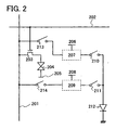
- FIG 2 schematically shows one embodiment mode of a pixel included in a display device of the present invention.
- a data line 201 and a scanning line 202 are provided;
- a first switch 213 for writing a data signal into the first comparator 207 and a second switch 214 for writing a data signal into the second comparator 209 are provided.
- a first reference potential 206 that is compared with a data potential is input to the first comparator 207, and a second reference potential 208 that is compared with a data potential is input to the second comparator 209.
- a third switch 210 and a fourth switch 211 by which it is determined which of the first comparator 207 and the second comparator 209 is selected to transmit output to the light-emitting element 212, are provided.
- a first terminal of the transistor 203 is connected to the data line 201, and a first electrode of the liquid crystal element 204 is connected to a second terminal of the transistor 203.
- a gate terminal of the transistor 203 is connected to the scanning line 202.
- a second electrode of the liquid crystal element 204 is connected to the counter electrode 205.
- Input of the first comparator 207 is connected to the data line 201 through the first switch 213, and output of the first comparator 207 is connected to a first electrode of the light-emitting element 212 through the third switch 210.
- input of the second comparator 209 is connected to the data line 201 through the second switch 214, and output of the second comparator 209 is connected to the first electrode of the light-emitting element 212 through the fourth switch 211.
- first reference potential 206 which is compared with a data potential is applied to the first comparator 207, and the second reference potential 208 is similarly applied to the second comparator 209.
- a data potential written into the liquid crystal element 204 from the data line 201 is input to the second comparator 209 and the first comparator 207.
- the first comparator 207 compares the data potential input from the data line with the first reference potential 206.
- the second comparator 209 compares the data potential input from the data line with the second reference potential 208.
- the first switch 213 writes a signal from the data line 201 into the first comparator 207
- the second switch 214 writes a signal from the data line 201 into the second comparator 209.
- the third switch 210 and the fourth switch 211 By the third switch 210 and the fourth switch 211, one of output of the first comparator 207 and output of the second comparator 209 is selected, and the output is transmitted to the light-emitting element 212. Therefore, it is necessary to set an operation timing appropriately so as not to turn on the third switch 210 and the fourth switch 211 at the same time.
- FIGS. 10A and 10B show operations of the circuit shown in FIG 2 .
- FIG. 10A shows an operation in a case where a negative potential is loaded from the data line 201 to the comparator.
- the first switch 213 is turned on, a data potential is written into the first comparator 207, the data potential is compared with the first reference potential 206 in the first comparator 207, and the third switch 210 is turned on so that output of the first comparator 207 is output to the light-emitting element 212.
- the second switch 214 and the fourth switch 211 which are connected to input and output of the second comparator 209 respectively are turned off.
- FIG 10B shows an operation in a case where a positive potential is loaded from the data line 201 to the comparator.
- the second switch 214 is turned on, a data potential is written into the second comparator 209, the data potential is compared with the second reference potential 208 in the second comparator 209, and the fourth switch 211 is turned on so that output of the second comparator 209 is output to the light-emitting element 212.
- the first switch 213 and the third switch 210 which are connected to input and output of the first comparator 207 respectively are turned off.
- the light-emitting element 212 may be an LED, an organic EL element, or the like. That is, any light-emitting element which can be controlled by a voltage, a current, or the like may be used.
- the switch can be an electrical switch or a mechanical switch. That is, any switch may be used as long as it can control a current flow, and the switch may be a transistor, a diode, or a logic circuit combining a transistor and a diode. Therefore, in a case where a transistor is used as the switch, polarity (conductivity type) thereof is not particularly limited because the transistor operates just as a switch. However, when a low off-state current is desired, a transistor of polarity with a lower off-state current is desirably used. For example, a transistor which is provided with an LDD region, a transistor which has a multi-gate structure, or the like has a low off-state current.
- an n-channel transistor be employed when a potential of a source terminal of a transistor operating as a switch is close to a potential of a low potential side power source (such as VSS, GND, or 0 V), while a p-channel transistor be employed when the potential of the source terminal is close to a potential of a high potential side power source (such as VDD).
- a CMOS type switch using both an n-channel transistor and a p-channel transistor may also be used.
- VDD is regarded as a high power source potential
- VSS is regarded as a low power source potential.
- the high power source potential VDD is to be higher than the low power source potential VSS.
- FIG 3 shows an example of a detailed circuit diagram of the pixel shown in FIG 2 .
- the circuit shown in FIG 3 has a feature in that two CMOS chopper inverter circuits are used as comparators.
- a first comparator 326 and a second comparator 327 are used.
- the first comparator 326 includes a first capacitor element 318; a first transistor 317; a first inverter including a second transistor 319 and a third transistor 320; and a second inverter including a fourth transistor 321 and a fifth transistor 322.
- the second comparator 327 includes a second capacitor element 314; a sixth transistor 313; and a third inverter including a seventh transistor 315 and an eighth transistor 316.
- a first reference potential line 301, a second reference potential line 303, and a data line 302 are provided.
- a scanning line 306, a first comparator initializing line 307, a second comparator initializing line 305, a comparator selecting line 304, a first data loading line 331, and a second data loading line 330 are provided.
- a ninth transistor 308 which writes a data voltage into a liquid crystal element 310 and a counter electrode 311 of the liquid crystal element are provided.
- a tenth transistor 312 and an eleventh transistor 329 which perform writing to the first comparator 326 are provided.
- a twelfth transistor 309 and a thirteenth transistor 328 which perform writing to the second comparator 327 are provided.
- a fourteenth transistor 324 which transmits output of the first comparator 326 to a light-emitting element 325 and a fifteenth transistor 323 which transmits output of the second comparator 327 to the light-emitting element 325 are provided.
- the second transistor 319 is a p-channel transistor and the third transistor 320 is an n-channel transistor;
- the fourth transistor 321 is a p-channel transistor and the fifth transistor 322 is an n-channel transistor;
- the seventh transistor 315 is a p-channel transistor and the eighth transistor 316 is an n-channel transistor.
- a first terminal of the ninth transistor 308, a first terminal of the thirteenth transistor 328, and a first terminal of the eleventh transistor 329 are connected to the data line 302.
- a second terminal of the ninth transistor 308 is connected to a first electrode of the liquid crystal element 310, and a gate terminal of the ninth transistor 308 is connected to the scanning line 306.
- the counter electrode 311 is connected to a second electrode of the liquid crystal element 310.
- a first terminal of the twelfth transistor 309 is connected to the second reference potential line 303.
- a second terminal of the thirteenth transistor 328 and a second terminal of the twelfth transistor 309 are connected to a first electrode of the second capacitor element 314 in the second comparator 327.
- a gate terminal of the thirteenth transistor 328 is connected to the second data loading line 330, and a gate terminal of the twelfth transistor 309 is connected to the second comparator initializing line 305.
- the seventh transistor 315 and the eighth transistor 316 form an inverter.
- a gate terminal of the seventh transistor 315 and a gate terminal of the eighth transistor 316 are connected to a second electrode of the second capacitor element 314 and a first terminal of the sixth transistor 313.
- a second terminal of the seventh transistor 315 and a second terminal of the eighth transistor 316 are connected to a second terminal of the sixth transistor 313 and a first terminal of the fifteenth transistor 323.
- a gate terminal of the sixth transistor 313 is connected to the second comparator initializing line 305.
- a first terminal of the tenth transistor 312 is connected to the first reference potential line 301.
- a gate terminal of the tenth transistor 312 is connected to the first comparator initializing line 307.
- a second terminal of the eleventh transistor 329 and a second terminal of the tenth transistor 312 are connected to a first electrode of the first capacitor element 318 in the first comparator 326.
- a gate terminal of the eleventh transistor 329 is connected to the first data loading line 331.
- the second transistor 319 and the third transistor 320 form an inverter.
- a gate terminal of the second transistor 319 and a gate terminal of the third transistor 320 are connected to a second electrode of the first capacitor element 318 and a first terminal of the first transistor 317.
- a second terminal of the second transistor 319 and a second terminal of the third transistor 320 are connected to a second terminal of the first transistor 317 and gate terminals of the fourth transistor 321 and the fifth transistor 322 which form another inverter.
- a second terminal of the fourth transistor 321 and a second terminal of the fifth transistor 322 are connected to a first terminal of the fourteenth transistor 324.
- a gate terminal of the first transistor 317 is connected to the first comparator initializing line 307.
- a gate terminal of the fifteenth transistor 323 and a gate terminal of the fourteenth transistor 324 are connected to the comparator selecting line 304.
- a second terminal of the fifteenth transistor 323 and a second terminal of the fourteenth transistor 324 are connected to a first electrode of the light-emitting element 325.
- the first comparator 326 compares a potential V ref1 of the first reference potential line 301 with a potential of the data line 302 when a negative voltage is applied to the liquid crystal element 310. If the potential of the data line 302 is higher than Vref1, a power source voltage VDD is output. On the other hand, if the potential of the data line 302 is lower than Vref1, 0 V is output.
- the second comparator 327 compares a potential Vref2 of the second reference potential line 303 with a potential of the data line 302 when a positive voltage is applied to the liquid crystal element 310. If the potential of the data line 302 is lower than Vref2, a power source voltage VDD is output.
- CMOS chopper inverter circuit is used as a comparator; however, any circuit may be used as long as its function is achieved.
- the fifteenth transistor 323 is a switch for determining whether the output of the second comparator 327 is output to the light-emitting element 325.
- the fourteenth transistor 324 is a switch for determining whether the output of the first comparator 326 is output to the light-emitting element 325.
- a signal may be given to the comparator selecting line 304 so that the fifteenth transistor 323 is turned on when the potential of the data line 302 is positive, and the fourteenth transistor 324 is turned on when the potential of the data line 302 is negative.
- a signal may be given to the comparator selecting line 304 so that the fifteenth transistor 323 is turned on when the potential of the data line 302 is negative, and the fourteenth transistor 324 is turned on when the potential of the data line 302 is positive.
- a period during which either the fifteenth transistor 323 or the fourteenth transistor 324 is turned on by a signal from the comparator selecting line 304 is regarded as a period during which the scanning line 306 is active, a data potential is loaded to the pixel circuit, and either the first comparator 326 or the second comparator 327 is initialized.
- the fifteenth transistor 323 and the fourteenth transistor 324 are required to have different polarity (conductivity type) from each other so that they are not turned on at the same time. A detailed operation timing of each transistor will be described later.
- the twelfth transistor 309 When a signal is input to the second comparator initializing line 305, the twelfth transistor 309 is turned on, and Vref2 is loaded to initialize the second comparator 327.
- the tenth transistor 312 When a signal is input to the first comparator initializing line 307, the tenth transistor 312 is turned on, and Vref1 is loaded to initialize the first comparator 326. It is necessary to set timings appropriately to input signals to the first comparator initializing line 307 and the second comparator initializing line 305 so that the twelfth transistor 309 and the tenth transistor 312 are not turned on at the same time.
- the thirteenth transistor 328 and the eleventh transistor 329 write a data potential, which is written into the liquid crystal element 310, into the initialized comparators.
- the thirteenth transistor 328 writes a data potential into the second comparator 327 when the data potential is positive
- the eleventh transistor 329 writes a data potential into the first comparator 326 when the data potential is negative.
- a timing which turns on either the thirteenth transistor 328 or the eleventh transistor 329 is required to be synchronized with a timing which makes the scanning line 306 active and turns on the ninth transistor 308 which performs writing to the liquid crystal element. Details of the timings will be described later.
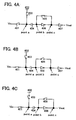
- FIGS. 4A and 4B are diagrams each explaining an operation of the first comparator 326 shown in FIG. 3 .
- Each element shown in FIGS. 4A and 4B corresponds to the element shown in FIG 3 .
- a first switch 401, a second switch 403, and a third switch 405 show operations of the eleventh transistor 329, the tenth transistor 312, and the first transistor 317, respectively.
- a reference potential 402 corresponds to Vref1.
- a first inverter 406 corresponds to the inverter including the second transistor 319 and the third transistor 320.
- a second inverter 407 corresponds to the inverter including the fourth transistor 321 and the fifth transistor 322.
- An input voltage Vin indicates an input voltage from the data line 302.
- the second switch 403 and the third switch 405 are turned on, and the first switch 401 is turned off, whereby the comparator is initialized.
- a potential of a logic threshold value (hereinafter denoted by Vth_inv) of the first inverter 406 is applied to a point b.
- Vth_inv a logic threshold value of the first inverter 406
- the reference potential 402 is Vref1
- Vref1 is applied to a point a.
- a voltage of Vref1 - Vth_inv is retained between both electrodes of a capacitor 404.
- the logic threshold value of the inverter is defined as a voltage which makes an input voltage and an output voltage of the inverter equal to each other.
- the comparator is required to be initialized because the logic threshold value of the inverter possibly varies from one pixel to another pixel due to variation in size or threshold value of the transistor included in the inverter. Initialization of the comparator can eliminate an adverse effect due to the logic threshold value of the inverter, which varies from one pixel to another pixel.
- a potential at the point a is equivalent to an input voltage Vin.
- a potential at the point b falls from the potential at the point a by the voltage retained between the both electrodes of the capacitor 404 and becomes Vin - (Vref1 - Vth_inv), which is represented by the following expression (1). Vin + Vth - ⁇ inv - Vref ⁇ 1
- Vc a potential at a point c that is output of the first inverter 406 (referred to as Vc) is determined depending on which of the potential at the point b (referred to as Vb) represented by the expression (1) and Vth_inv is high.
- Vb a potential at which of the potential at the point b represented by the expression (1) and Vth_inv is high.
- Vb > Vth_inv 0 V is output as Vc.
- VDD is output as Vc
- logic is further inverted by the second inverter 407 so that 0 V is output as Vout.
- VDD is output in the case of Vin > Vref1
- 0 V is output in the case of Vin ⁇ Vref1.
- FIG 4C is a diagram explaining an operation of the second comparator 327.
- the operation of the second comparator 327 is different from that of the first comparator 326 in that the inverter 407 is not provided, and the potential at the point c is equivalent to a value of the output voltage Vout.
- Each element shown in FIG 4C corresponds to the element shown in FIG 3 .
- a first switch 401, a second switch 403, and a third switch 405 show operations of the thirteenth transistor 328, the twelfth transistor 309, and the sixth transistor 313, respectively.
- a reference potential 402 corresponds to Vref2.
- An inverter 406 corresponds to the inverter including the seventh transistor 315 and the eighth transistor 316.
- An input voltage Vin indicates an input voltage from the data line 302.
- Vb has a value represented by the following expression (2).
- Vin in the case of Vin > Vref2, 0 V is output as Vout.
- Vin in the case of Vin ⁇ Vref2, VDD is output as Vout.
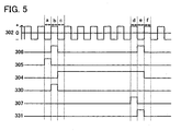
- FIG 5 shows a timing of each control signal of the circuit shown in FIG. 3 . That is, each signal line of the data line 302, the scanning line 306, the second comparator initializing line 305, the first comparator initializing line 307, the second data loading line 330, the first data loading line 331, and the comparator selecting line 304 will be explained.
- a signal of the data line 302 is an AC signal, and a potential of a data signal which is written into one pixel is inverted to be positive or negative in every writing operation.
- the scanning line 306 has a high potential, and writing is performed to the liquid crystal element, but the potential of the data line 302 in the period b and the potential of the data line 302 in the period e are inverted.
- a writing operation of a data signal having a positive potential into the liquid crystal element is performed in the periods a, b, and c of FIG 5 .
- a positive potential is written from the data line 302
- a high potential is applied to the second comparator initializing line 305 in the period a to initialize the second comparator 327
- Vref2 is also applied to the second capacitor element 314 to initialize the second comparator 327.
- a high potential is applied to the second data loading line 330 in the period b, the thirteenth transistor 328 is turned on, and a data potential which is written into the liquid crystal element 310 is written into the second comparator 327.
- a high potential is applied to the comparator selecting line 304 in the period c, the fifteenth transistor 323 is turned on, the fourteenth transistor 324 is turned off, and the output of the second comparator 327 is transmitted to the light-emitting element 325.
- a writing operation of a data signal having a negative potential into the liquid crystal element is performed in the periods d, e, and f of FIG 5 .
- a negative potential is written from the data line 302
- a high potential is applied to the first comparator initializing line 307 in the period d to initialize the first comparator 326
- Vref1 is applied to the capacitor element 318 to initialize the first comparator 326.
- a high potential is applied to the first data loading line 331 in the period e, the eleventh transistor 329 is turned on, and a data potential which is written into the liquid crystal element is written into the first comparator 326.
- a low potential is applied to the comparator selecting line 304 in the period f, the fourteenth transistor 324 is turned on, the fifteenth transistor 323 is turned off, and the output of the first comparator 326 is transmitted to the light-emitting element 325.
- a backlight when black is displayed in a display device using a liquid crystal, a backlight is made not to emit light; therefore, light leakage can be eliminated and the contrast can be improved.
- a backlight is arranged in each pixel and a function to control a lighting state of a light-emitting element based on each pixel is provided in a pixel circuit; therefore, a malfunction can be avoided, in which, when a backlight is turned off for a pixel displaying black, all other pixels also display black.
- a backlight in a portion where lighting is not needed can be individually turned off; therefore, power savings can be effectively achieved.
- FIG 6 schematically shows a circuit in which one comparator is removed from the circuit of Embodiment Mode 1.
- a data line 601 and a scanning line 602 are provided.
- a transistor 603 which performs writing to a liquid crystal element 604 and a counter electrode 605 are provided.
- a light-emitting element 612 used as a backlight is provided.
- a first switch 613 which writes a data signal into a comparator 608 is provided.
- a first reference potential 606 and a second reference potential 607 which are compared with a data potential are provided.
- a second switch 609 and a third switch 610 by which it is determined which of positive and negative outputs is output from the comparator to the light-emitting element, are provided.
- a first terminal of the transistor 603 is connected to the data line 601, and a first electrode of the liquid crystal element 604 is connected to a second terminal of the transistor 603.
- a gate terminal of the transistor 603 is connected to the scanning line 602.
- a first terminal of the first switch 613 is connected to the data line 601.
- a second electrode of the liquid crystal element 604 is connected to the counter electrode 605.
- the comparator 608 is connected to a second terminal of the first switch 613.
- the second switch 609 and an inverter 611 are connected to output of the comparator 608.
- the output of the comparator 608 is connected to the light-emitting element 612 through the second switch 609, and the third switch 610 is connected to output of the inverter 611 and the light-emitting element 612.
- the first reference potential 606 and the second reference potential 607 which are compared with a data potential are connected to the comparator 608.
- a data potential written into the liquid crystal element 604 is also input to the comparator 608 through the first switch 613.
- the comparator 608 compares the data potential input from the data line 601 with a voltage of the first reference potential 606 or the second reference potential 607.
- a negative voltage is applied to the liquid crystal element 604 in a normally white liquid crystal
- a value of the data potential input from the data line 601 is compared with a value of the first reference potential 606.
- the third switch 610 is turned on, and the output of the comparator 608, in which logic is inverted by the inverter 611, is transmitted to the light-emitting element 612.
- a power source voltage VDD is output to the light-emitting element 612.
- 0 V is output.
- the comparator 608 compares the second reference potential 607 with the potential of the data line 601 when a positive voltage is applied to the liquid crystal element 604 in the normally white liquid crystal. At that time, the second switch 609 is turned on, and the output of the comparator is transmitted to the light-emitting element 612. If the potential of the data line 601 is lower than the second reference potential 607, a power source voltage VDD is output to the light-emitting element 612. On the other hand, if the potential of the data line 601 is higher than the second reference potential 607, 0 V is output.
- the light-emitting element 612 may be an LED, an organic EL element, or the like. That is, any light-emitting element which can be controlled by a voltage, a current, or the like may be used.
- FIG 7 shows an example of a detailed circuit diagram of the pixel shown in FIG 6 .
- a data line 702 and a scanning line 704 are provided.
- a first transistor 709 which performs writing to a liquid crystal element 711 and a counter electrode 712 are provided.
- the circuit shown in FIG 7 has a feature in that one CMOS chopper inverter circuit is used as a comparator. In other words, a comparator 722 is used.
- the comparator 722 includes a capacitor element 726; a second transistor 714; and a first inverter including a third transistor 715 and a fourth transistor 716.
- a first reference potential line 701, a second reference potential line 703, and the data line 702 are provided.
- the scanning line 704, a comparator initializing line 705, a second reference potential selecting line 706, a first reference potential selecting line 707, a first light-emitting element driving signal selecting line 708, a second light-emitting element driving signal selecting line 725, and a data-loading line 724 are provided.
- a fifth transistor 710, a sixth transistor 723, and a seventh transistor 713 which perform writing to the comparator 722 are provided.
- An eighth transistor 719 and a ninth transistor 720 which transmit output of the comparator to a light-emitting element are provided.
- a second inverter including a tenth transistor 717 and an eleventh transistor 718 is provided.
- a light-emitting element 721 used as a backlight is provided. It is to be noted that the tenth transistor 717 is a p-channel transistor and the eleventh transistor 718 is an n-channel transistor.
- a first terminal of the first transistor 709 and a first terminal of the sixth transistor 723 are connected to the data line 702.
- a second terminal of the first transistor 709 is connected to a first electrode of the liquid crystal element 711, and a gate terminal of the first transistor 709 is connected to the scanning line 704.
- a second electrode of the liquid crystal element 711 is connected to the counter electrode 712.
- a first terminal of the seventh transistor 713 is connected to the first reference potential line 701.
- a first terminal of the fifth transistor 710 is connected to the second reference potential line 703.
- a second terminal of the seventh transistor 713, a second terminal of the sixth transistor 723, and a second terminal of the fifth transistor 710 are connected to a first electrode of the capacitor element 726 in the comparator 722.
- a gate terminal of the sixth transistor 723 is connected to the data loading line 724, and a gate terminal of the first transistor 709 is connected to the scanning line 704.
- a gate terminal of the fifth transistor 710 is connected to the second reference potential selecting line 706, and a gate terminal of the seventh transistor 713 is connected to the first reference potential selecting line 707.
- the first inverter includes the third transistor 715 and the fourth transistor 716. Gate terminals of these two transistors are connected to a second electrode of the capacitor element 726 and a first terminal of the second transistor 714.
- a second terminal of the third transistor 715 and a second terminal of the fourth transistor 716 are connected to a second terminal of the second transistor 714, a first terminal of the eighth transistor 719, and gate terminals of the tenth transistor 717 and the eleventh transistor 718 included in the second inverter.
- a second terminal of the tenth transistor 717 and a second terminal of the eleventh transistor 718 are connected to a first terminal of the ninth transistor 720.
- a gate terminal of the second transistor 714 is connected to the comparator initializing line 705.
- a gate terminal of the eighth transistor 719 is connected to the second light-emitting element driving signal selecting line 725, and a gate terminal of the ninth transistor 720 is connected to the first light-emitting element driving signal selecting line 708.
- a second terminal of the eighth transistor 719 and a second terminal of the ninth transistor 720 are connected to a first electrode of the light-emitting element 721.
- the fifth transistor 710 is turned on and transmits a potential Vref2 of the second reference potential line 703 to the comparator 722.
- the seventh transistor 713 is turned on and transmits a potential Vref1 of the first reference potential line 701 to the comparator 722.
- the comparator initializing line 705 has a high potential
- the second transistor 714 is turned on, and the comparator 722 is initialized. An operation in the comparator 722 is similar to that of the comparator 326.
- the sixth transistor 723 When the data loading line 724 has a high potential, the sixth transistor 723 is turned on and writes a data potential which is written into the liquid crystal element 711 also into the initialized comparator 722.
- the eighth transistor 719 When the second light-emitting element driving signal selecting line 725 has a high potential, the eighth transistor 719 is turned on and transmits output of the comparator 722, which is obtained when Vref2 is compared with a potential of the data line 702, to the light-emitting element 721.
- the ninth transistor 720 When the first light-emitting element driving signal selecting line 708 has a high potential, the ninth transistor 720 is turned on and transmits output of the comparator 722, which is obtained when Vref1 is compared with a potential of the data line 702, to the light-emitting element 721.
- a CMOS chopper inverter circuit is used as a comparator; however, any circuit may be used as long as its function is achieved.
- FIG 8 shows a timing of each control signal of the circuit shown in FIG. 7 . That is, each signal line of the data line 702, the scanning line 704, the comparator initializing line 705, the second reference potential selecting line 706, the first reference potential selecting line 707, the data loading line 724, the second light-emitting element driving signal selecting line 725, and the first light-emitting element driving signal selecting line 708 will be explained.
- a signal of the data line 702 is an AC signal, and a potential of a data signal which is written into one pixel is inverted to be positive or negative in every writing operation.
- the scanning line 704 has a high potential, and writing is performed to the liquid crystal element, but the potential of the data line 702 in the period b and the potential of the data line 702 in the period e are inverted.
- a writing operation of a data signal having a positive potential into the liquid crystal element is performed in the periods a, b, and c of FIG 8 .
- a positive potential is written from the data line 702
- a high potential is applied to the comparator initializing line 705 in the period a to initialize the comparator 722.
- a high potential is applied to the second reference potential selecting line 706, and Vref2 is applied to the capacitor element 726.
- a high potential is applied to the data loading line 724 in the period b, the sixth transistor 723 is turned on, and a data potential which is written into the liquid crystal element 711 is also written into the comparator 722. Further, a high potential is applied to the second light-emitting element driving signal selecting line 725 in the period c, the eighth transistor 719 is turned on, and output of the comparator 722 is transmitted to the light-emitting element 721.
- a writing operation of a data signal having a negative potential into the liquid crystal element is performed in the periods d, e, and f of FIG 8 .
- a negative potential is written from the data line 702
- a high potential is applied to the comparator initializing line 705 in the period d to initialize the comparator 722.
- a high potential is applied to the first reference potential selecting line 707, and Vref1 is applied to the capacitor element 726.
- a high potential is applied to the data loading line 724 in the period e, the sixth transistor 723 is turned on, and a data potential which is written into the liquid crystal element 711 is written into the comparator 722. Further, a high potential is applied to the first light-emitting element driving signal selecting line 708 in the period f, the ninth transistor 720 is turned on, and the output of the comparator 722 is transmitted to the light-emitting element 721 through the tenth transistor 717 and the eleventh transistor 718 included in the second inverter.
- both the first light-emitting element driving signal selecting line 708 and the second light-emitting element driving signal selecting line 725 have low potentials. This is because there is a period during which logic is indefinite after the comparator is initialized and until the output is determined. Since the light-emitting element is always turned off in this period, the period is preferably suppressed to be so short that it cannot be recognized by human eyes.
- a backlight is made not to emit light; therefore, light leakage can be eliminated and the contrast can be improved.
- a backlight is arranged in each pixel and a function to control a lighting state of a light-emitting element based on each pixel is provided in a pixel circuit; therefore, a malfunction can be avoided, in which, when a backlight is turned off for a pixel displaying black, all other pixels also display black.
- a backlight in a portion where lighting is not needed can be individually turned off; therefore, power savings can be effectively achieved.
- one comparator is removed from the circuit shown in Embodiment Mode 1, and thus, the number of transistors included in the circuit can be reduced, whereby an advantage such as a higher aperture ratio of the pixel can also be obtained.
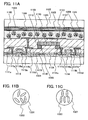
- FIG. 11A shows a comparative display device. Over a glass substrate 1101, a base film 1115 is formed, and a liquid crystal element driving transistor 1113 and a light-emitting element driving transistor 1114 are formed thereover.
- the liquid crystal element driving transistor 1113 includes a first impurity region 1117a and a second impurity region 1117b.
- a first channel region 1116a is formed between the first impurity region 1117a and the second impurity region 1117b.
- a gate insulating film 1118 is formed over the first impurity region 1117a, the second impurity region 1117b, and the first channel region 1116a.
- a first gate electrode 1119a is formed over the gate insulating film 1118.
- the light-emitting element driving transistor 1114 includes a third impurity region 1117c and a fourth impurity region 1117d.
- a second channel region 1116b is formed between the third impurity region 1117c and the fourth impurity region 1117d.
- the gate insulating film 1118 is formed over the third impurity region 1117c, the fourth impurity region 1117d, and the second channel region 1116b.
- a second gate electrode 1119b is formed over the gate insulating film 1118.
- a first interlayer film 1109 is formed, and a first electrode 1111a, a second electrode 1111b, a third electrode 1111c, a fourth electrode 1111d, and a first wiring 1120 are formed.
- An anisotropic conductive particle 1112 is provided over each of the third electrode 1111c and the first wiring 1120, and a light-emitting diode 1110 is provided thereover.
- the light-emitting diode 1110 is a white light-emitting diode
- color display can be performed by combining the light-emitting diode 1110 and a color filter.
- the light-emitting diodes 1110 emitting light of red (R), green (G), and blue (B) may be each provided in a pixel to perform color display.
- the light-emitting diode may be combined with a color filter to improve color purity.
- a second interlayer film 1108 is formed over the first interlayer film 1109.
- a pixel electrode 1107 is formed over the second interlayer film 1108, and a liquid crystal layer 1306 is provided thereover.
- An alignment film 1121 is provided over the liquid crystal layer 1306, a counter electrode 1105 is formed thereover, and a light-shielding layer 1103 and a color filter 1104 are provided thereover.
- a glass substrate 1102 that is a counter substrate is provided over the light-shielding layer 1103 and the color filter 1104.
- a polymer dispersed liquid crystal is preferably used for the liquid crystal layer 1306. As shown in FIG. 11B , the polymer dispersed liquid crystal is a liquid crystal in which liquid crystals 1322 are dispersed in a polymer 1321.
- the components in FIG 11A are connected as follows.
- the first impurity region 1117a is connected to the first electrode 1111a
- the second impurity region 1117b is connected to the second electrode 1111b.
- the second electrode 1111b is connected to the pixel electrode 1107.
- the third impurity region 1117c is connected to the third electrode 1111c
- the fourth impurity region 1117d is connected to the fourth electrode 1111d.
- the third electrode 1111c is connected to a first electrode 1122 of the light-emitting diode 1110 through the anisotropic conductive particle 1112.
- a second electrode 1123 of the light-emitting diode 1110 is connected to the first wiring 1120 through the anisotropic conductive particle 1112. It is to be noted that other substances such as solder may be used instead of the anisotropic conductive particle 1112 without limitation to the anisotropic conductive particle, as long as the substances can electrically connect the components.
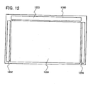
- FIG. 12 shows a block diagram of the display device.
- the display device shown in FIG. 12 includes a pixel portion 1201 including a plurality of pixels each having a light-emitting element, a scanning line driving circuit 1202 selecting each pixel, a data line driving circuit 1203 controlling input of a data signal to a selected pixel, and a comparator driving circuit 1204 controlling a comparator in each pixel over a substrate 1200.
- a backlight when black is displayed in a display device using a liquid crystal, a backlight is made not to emit light; therefore, light leakage can be eliminated and the contrast can be improved.
- a backlight is arranged in each pixel and a function to control a lighting state of a light-emitting element based on each pixel is provided in a pixel circuit; therefore, a malfunction can be avoided, in which, when a backlight is turned off for a pixel displaying black, all other pixels also display black.
- a backlight in a portion where lighting is not needed can be individually turned off; therefore, power savings can be effectively achieved.
- Electronic devices using the display device of the present invention include a camera such as a video camera or a digital camera, a goggle type display (head mounted display), a navigation system, an audio reproducing device (such as a car audio stereo or an audio component set), a laptop personal computer, a game machine, a portable information terminal (such as a mobile computer, a mobile phone, a portable game machine, or an electronic book), an image reproducing device provided with a storage medium (specifically, a device for reproducing a storage medium such as a digital versatile disc (DVD) and having a display for displaying the reproduced image), and the like. Specific examples of such electronic devices are shown in FIGS. 9A to 9H .
- FIG 9A shows a television device, which includes a housing 901, a supporting base 902, a display portion 903, speaker portions 904, a video input terminal 905, and the like.
- the present invention can be applied to a display device which forms the display portion 903.
- an image with the improved contrast can be provided.
- This television device can be used for receiving TV broadcast as well as for a monitor of a video game machine, computer, or the like.
- FIG 9B shows a digital still camera, which includes a main body 906, a display portion 907, an image receiving portion 908, operation keys 909, an external connecting port 910, a shutter release button 911, and the like.
- the present invention can be applied to a display device which forms the display portion 907.
- an image with the improved contrast can be provided.
- FIG 9C shows a laptop personal computer, which includes a main body 912, a housing 913, a display portion 914, a keyboard 915, an external connecting port 916, a pointing device 917, and the like.
- the present invention can be applied to a display device which forms the display portion 914.
- an image with the improved contrast can be provided.
- FIG 9D shows a mobile computer, which includes a main body 918, a display portion 919, a switch 920, operation keys 921, an infrared port 922, and the like.
- the present invention can be applied to a display device which forms the display portion 919.
- an image with the improved contrast can be provided.
- FIG 9E shows a portable image reproducing device provided with a storage medium (specifically, a DVD player), which includes a main body 923, a housing 924, a display portion A 925, a display portion B 926, a storage medium (such as DVD) reading portion 927, operation keys 928, a speaker portion 929, and the like.
- the display portion A 925 mainly displays image data
- the display portion B 926 mainly displays text data.
- the present invention can be applied to display devices which form the display portion A 925 and the display portion B 926.
- an image with the improved contrast can be provided.
- the image reproducing device provided with a storage medium also includes a home-use game machine and the like.
- FIG 9F shows a goggle type display (head mounted display), which includes a main body 930, a display portion 931, an arm portion 932, and the like.
- the present invention can be applied to a display device which forms the display portion 931.
- an image with the improved contrast can be provided.
- FIG 9G shows a video camera, which includes a main body 933, a display portion 934, a housing 935, an external connecting port 936, a remote control receiving portion 937, an image receiving portion 938, a battery 939, an audio input portion 940, operation keys 941, and the like.
- the present invention can be applied to a display device which forms the display portion 934.
- an image with the improved contrast can be provided.
- FIG 9H shows a mobile phone, which includes a main body 942, a housing 943, a display portion 944, an audio input portion 945, an audio output portion 946, operation keys 947, an external connecting port 948, an antenna 949, and the like.
- the present invention can be applied to a display device which forms the display portion 944. It is to be noted that current consumption of the mobile phone can be suppressed by display of white text on a black background in the display portion 944. In accordance with the present invention, an image with the improved contrast can be provided.
- the display device can be applied to a front projector or a rear projector in which light including output image data is magnified and projected with a lens or the like.
- a light-emitting device consumes power in its light-emitting portion, it is desirable to display data so that the light-emitting portion is as small as possible.
- a light-emitting device is used in a display portion of a portable information terminal such as a mobile phone or an audio reproducing device, which mainly displays text data, it is desirable to drive the device so that text data is formed by using a light-emitting portion with a non-light-emitting portion on the background.
Claims (6)
- Dispositif d'affichage comprenant:un pixel comprenant un élément électroluminescent (212) utilisé comme un rétro-éclairage et un élément à cristaux liquides (204) superposé à l'élément électroluminescent (212) et dans lequel la lumière émise par l'élément électroluminescent (212) traverse l'élément à cristaux liquides (204);une ligne de données (201) reliée électriquement à l'élément à cristaux liquides (204);ledit pixel étant caractérisé en ce qu'il comprend aussi:un premier comparateur (207) avec une première entrée reliée électriquement à la ligne de données (201) par un premier commutateur (213), avec une seconde entrée reliée électriquement à un premier potentiel de référence qui est défini comme la limite supérieure de la plage de tension de données dans laquelle une image noire est affichée, et avec une sortie reliée électriquement à une première électrode de l'élément électroluminescent (212) par un troisième commutateur (210);un second comparateur (209) avec une première entrée reliée électriquement à la ligne de données (201) par un second commutateur (214), une seconde entrée reliée électriquement à un second potentiel de référence qui est défini comme la limite inférieure de la plage de tension de données dans laquelle une image noire est affichée, et avec une sortie reliée électriquement à la première électrode de l'élément électroluminescent (212) par un quatrième commutateur (211);le dispositif d'affichage étant disposé de la manière suivante:quand le potentiel de la ligne de données (201) a une valeur négative:le premier commutateur et le troisième commutateur sont fermés et le second commutateur et le quatrième commutateur sont ouverts afin quele premier comparateur (207) compare le potentiel de la ligne de données (201) avec le premier potentiel de référence, transmette la tension qui éteint la lumière dudit élément électroluminescent (212) quand le potentiel de la ligne de données est inférieur au premier potentiel de référence et transmette la tension qui allume la lumière dudit élément électroluminescent (212) quand le potentiel de la ligne de données est supérieur au premier potentiel de référence; etquand le potentiel de la ligne de données (201) a une valeur positive:le second commutateur et le quatrième commutateur sont fermés et le premier commutateur et le troisième commutateur sont ouverts afin quele second comparateur (209) compare le potentiel de la ligne de données (201) avec le second potentiel de référence, transmette la tension qui éteint la lumière dudit élément électroluminescent (212) quand le potentiel de la ligne de données est supérieur au second potentiel de référence et transmette la tension qui allume la lumière dudit élément électroluminescent (212) quand le potentiel de la ligne de données est inférieur au second potentiel de référence.
- Dispositif d'affichage selon la revendication 1, dans lequel la lumière traverse l'élément à cristaux liquides (204) qui a un mode d'affichage normalement blanc dans lequel la lumière est émise lorsque la tension n'est pas appliquée à l'élément à cristaux liquides ou qui a un mode d'affichage normalement noir dans lequel la lumière est émise lorsque la tension est appliquée à l'élément à cristaux liquides.
- Dispositif électronique comprenant le dispositif d'affichage selon la revendication 1 dans une portion d'affichage.
- Dispositif d'affichage selon la revendication 1, dans lequel un potentiel en fonction d'un signal analogique est appliqué à la ligne de données (201).
- Procédé de commande d'un dispositif d'affichage, qui comprend un pixel comprenant un élément électroluminescent (212) utilisé comme un rétro-éclairage et un élément à cristaux liquides (204) superposé à l'élément électroluminescent (212) et dans lequel la lumière émise par l'élément électroluminescent (212) traverse l'élément à cristaux liquides (204); une ligne de données (201) reliée électriquement à l'élément à cristaux liquides (204); dans lequel le pixel comprend aussi:un premier comparateur (207) avec une première entrée reliée électriquement à la ligne de données (201) par un premier commutateur (213), avec une seconde entrée reliée électriquement à un premier potentiel de référence qui est défini comme la limite supérieure de la plage de tension de données dans laquelle une image noire est affichée, et avec une sortie reliée électriquement à une première électrode de l'élément électroluminescent (212) par un troisième commutateur (210);un second comparateur (209) avec une première entrée reliée électriquement à la ligne de données (201) par un second commutateur (214), une seconde entrée reliée électriquement à un second potentiel de référence qui est défini comme la limite inférieure de la plage de tension de données dans laquelle une image noire est affichée, et avec une sortie reliée électriquement à la première électrode de l'élément électroluminescent (212) par un quatrième commutateur (211);le procédé comprenant les étapes de:appliquer un potentiel en fonction d'un signal analogique à la ligne de données (201) afin de commander l'élément à cristaux liquides (204);caractérisé en ce quequand le potentiel de la ligne de données (201) a une valeur négative:le premier commutateur et le troisième commutateur sont fermés et le second commutateur et le quatrième commutateur sont ouverts afin quele premier comparateur (207) compare le potentiel de la ligne de données (201) avec le premier potentiel de référence, transmette la tension qui éteint la lumière dudit élément électroluminescent (212) quand le potentiel de la ligne de données est inférieur au premier potentiel de référence et transmette la tension qui allume la lumière dudit élément électroluminescent (212) quand le potentiel de la ligne de données est supérieur au premier potentiel de référence; etquand le potentiel de la ligne de données (201) a une valeur positive:le second commutateur et le quatrième commutateur sont fermés et le premier commutateur et le troisième commutateur sont ouverts afin quele second comparateur (209) compare le potentiel de la ligne de données (201) avec le second potentiel de référence, transmette la tension qui éteint la lumière dudit élément électroluminescent (212) quand le potentiel de la ligne de données est supérieur au second potentiel de référence et transmette la tension qui allume la lumière dudit élément électroluminescent (212) quand le potentiel de la ligne de données est inférieur au second potentiel de référence.
- Procédé de commande d'un dispositif d'affichage selon la revendication 5, dans lequel la lumière traverse l'élément à cristaux liquides (204) qui a un mode d'affichage normalement blanc dans lequel la lumière est émise lorsque la tension n'est pas appliquée à l'élément à cristaux liquides ou qui a un mode d'affichage normalement noir dans lequel la lumière est émise lorsque la tension est appliquée à l'élément à cristaux liquides.
Applications Claiming Priority (1)
| Application Number | Priority Date | Filing Date | Title |
|---|---|---|---|
| JP2006112533 | 2006-04-14 |
Publications (3)
| Publication Number | Publication Date |
|---|---|
| EP1845514A2 EP1845514A2 (fr) | 2007-10-17 |
| EP1845514A3 EP1845514A3 (fr) | 2008-05-21 |
| EP1845514B1 true EP1845514B1 (fr) | 2013-10-02 |
Family
ID=38191254
Family Applications (1)
| Application Number | Title | Priority Date | Filing Date |
|---|---|---|---|
| EP20070006970 Not-in-force EP1845514B1 (fr) | 2006-04-14 | 2007-04-03 | Dispositif d'affichage et son procédé de commande |
Country Status (4)
| Country | Link |
|---|---|
| US (4) | US8159449B2 (fr) |
| EP (1) | EP1845514B1 (fr) |
| JP (8) | JP5322356B2 (fr) |
| CN (2) | CN102915707B (fr) |
Families Citing this family (53)
| Publication number | Priority date | Publication date | Assignee | Title |
|---|---|---|---|---|
| WO2009063797A1 (fr) * | 2007-11-14 | 2009-05-22 | Semiconductor Energy Laboratory Co., Ltd. | Dispositif d'affichage à cristaux liquides |
| FR2925746B1 (fr) * | 2007-12-21 | 2010-01-01 | Commissariat Energie Atomique | Dispositif d'affichage comportant des filtres colores et des elements photoemissifs alignes electroniquement |
| US8284218B2 (en) * | 2008-05-23 | 2012-10-09 | Semiconductor Energy Laboratory Co., Ltd. | Display device controlling luminance |
| WO2010018706A1 (fr) | 2008-08-11 | 2010-02-18 | シャープ株式会社 | Circuit d’attaque à charge capacitive et dispositif d'affichage utilisant ce circuit |
| KR101498094B1 (ko) * | 2008-09-29 | 2015-03-05 | 삼성디스플레이 주식회사 | 표시 장치 및 그 구동 방법 |
| TWI475544B (zh) * | 2008-10-24 | 2015-03-01 | Semiconductor Energy Lab | 顯示裝置 |
| KR102433488B1 (ko) | 2008-12-19 | 2022-08-18 | 가부시키가이샤 한도오따이 에네루기 켄큐쇼 | 표시장치의 구동방법 |
| KR101659427B1 (ko) * | 2009-02-06 | 2016-09-23 | 가부시키가이샤 한도오따이 에네루기 켄큐쇼 | 표시 장치 구동 방법 |
| JP5448981B2 (ja) | 2009-04-08 | 2014-03-19 | 株式会社半導体エネルギー研究所 | 液晶表示装置の駆動方法 |
| CN102034451A (zh) * | 2009-09-30 | 2011-04-27 | 乐金显示有限公司 | 液晶显示装置 |
| US9935622B2 (en) | 2011-04-28 | 2018-04-03 | Semiconductor Energy Laboratory Co., Ltd. | Comparator and semiconductor device including comparator |
| WO2013008765A1 (fr) | 2011-07-08 | 2013-01-17 | Semiconductor Energy Laboratory Co., Ltd. | Module électroluminescent, dispositif électroluminescent et procédé de fabrication du module électroluminescent |
| GB201114771D0 (en) * | 2011-08-26 | 2011-10-12 | Bae Systems Plc | A display |
| JP6050054B2 (ja) * | 2011-09-09 | 2016-12-21 | 株式会社半導体エネルギー研究所 | 半導体装置 |
| US10043794B2 (en) | 2012-03-22 | 2018-08-07 | Semiconductor Energy Laboratory Co., Ltd. | Semiconductor device and electronic device |
| TWI471839B (zh) * | 2012-04-03 | 2015-02-01 | Wintek Corp | 整合發光元件與電子書的顯示器與其驅動的方法 |
| JP2014032399A (ja) | 2012-07-13 | 2014-02-20 | Semiconductor Energy Lab Co Ltd | 液晶表示装置 |
| JP5877777B2 (ja) | 2012-09-26 | 2016-03-08 | 日立オートモティブシステムズ株式会社 | 回転電機、磁極ピース製造方法 |
| JP6538306B2 (ja) | 2013-03-20 | 2019-07-03 | 株式会社半導体エネルギー研究所 | 発光モジュール、発光装置 |
| US9710013B2 (en) | 2014-08-08 | 2017-07-18 | Semiconductor Energy Laboratory Co., Ltd. | Display panel, data processing device, program |
| KR102220553B1 (ko) * | 2015-03-10 | 2021-02-26 | 한국전자통신연구원 | 표시 패널 및 그것을 포함하는 표시 장치 |
| WO2016151429A1 (fr) | 2015-03-23 | 2016-09-29 | Semiconductor Energy Laboratory Co., Ltd. | Panneau d'affichage et dispositif de traitement d'informations |
| KR102494418B1 (ko) | 2015-04-13 | 2023-01-31 | 가부시키가이샤 한도오따이 에네루기 켄큐쇼 | 표시 패널, 데이터 처리 장치, 및 표시 패널의 제조방법 |
| WO2017025835A1 (fr) | 2015-08-07 | 2017-02-16 | Semiconductor Energy Laboratory Co., Ltd. | Panneau d'affichage, dispositif de traitement d'informations et procédé d'attaque d'un panneau d'affichage |
| JP6791661B2 (ja) * | 2015-08-07 | 2020-11-25 | 株式会社半導体エネルギー研究所 | 表示パネル |
| US10170528B2 (en) | 2015-08-07 | 2019-01-01 | Semiconductor Energy Laboratory Co., Ltd. | Display panel and manufacturing method thereof |
| TWI776519B (zh) | 2015-08-19 | 2022-09-01 | 日商半導體能源研究所股份有限公司 | 資訊處理裝置 |
| WO2017055971A1 (fr) | 2015-10-01 | 2017-04-06 | Semiconductor Energy Laboratory Co., Ltd. | Dispositif d'affichage et son procédé de fabrication |
| WO2017064587A1 (fr) | 2015-10-12 | 2017-04-20 | Semiconductor Energy Laboratory Co., Ltd. | Panneau d'affichage, dispositif d'entrée/sortie, processeur de données et procédé de fabrication de panneau d'affichage |
| WO2017064593A1 (fr) | 2015-10-12 | 2017-04-20 | Semiconductor Energy Laboratory Co., Ltd. | Dispositif d'affichage et son procédé de fabrication |
| WO2017068454A1 (fr) | 2015-10-23 | 2017-04-27 | Semiconductor Energy Laboratory Co., Ltd. | Panneau d'affichage, dispositif d'entrée/sortie et dispositif de traitement de données |
| WO2017081575A1 (fr) | 2015-11-11 | 2017-05-18 | Semiconductor Energy Laboratory Co., Ltd. | Dispositif d'affichage et son procédé de fabrication |
| US10540934B2 (en) | 2015-11-16 | 2020-01-21 | Samsung Electronics Co., Ltd. | Liquid crystal display device and driving method thereof |
| CN105609058B (zh) * | 2016-01-04 | 2018-09-04 | 京东方科技集团股份有限公司 | 背光源及显示装置 |
| WO2017125834A1 (fr) | 2016-01-18 | 2017-07-27 | Semiconductor Energy Laboratory Co., Ltd. | Dispositif d'entrée/sortie et processeur de données |
| JP6906978B2 (ja) | 2016-02-25 | 2021-07-21 | 株式会社半導体エネルギー研究所 | 半導体装置、半導体ウェハ、および電子機器 |
| JP6863803B2 (ja) | 2016-04-07 | 2021-04-21 | 株式会社半導体エネルギー研究所 | 表示装置 |
| KR102365543B1 (ko) * | 2016-06-10 | 2022-02-18 | 가부시키가이샤 한도오따이 에네루기 켄큐쇼 | 정보 단말 |
| TWI718208B (zh) | 2016-06-30 | 2021-02-11 | 日商半導體能源研究所股份有限公司 | 顯示裝置及其工作方法以及電子裝置 |
| TWI709952B (zh) | 2016-07-01 | 2020-11-11 | 日商半導體能源研究所股份有限公司 | 電子裝置、電子裝置的驅動方法 |
| US10332949B2 (en) | 2016-07-06 | 2019-06-25 | Seoul Semiconductor Co., Ltd. | Display apparatus |
| CN116775543A (zh) | 2016-09-06 | 2023-09-19 | 株式会社半导体能源研究所 | 电子设备 |
| JP2018054901A (ja) * | 2016-09-29 | 2018-04-05 | 株式会社半導体エネルギー研究所 | 表示システムおよび電子機器 |
| JP2018067217A (ja) * | 2016-10-21 | 2018-04-26 | 株式会社半導体エネルギー研究所 | 情報端末及び避難誘導システム |
| US10490130B2 (en) | 2017-02-10 | 2019-11-26 | Semiconductor Energy Laboratory Co., Ltd. | Display system comprising controller which process data |
| JP2019080312A (ja) | 2017-10-23 | 2019-05-23 | アスク インダストリーズ ソシエタ ペル アツィオーニAsk Industries Societa’ Per Azioni | 閉鎖型薄膜を有する拡声器及びその組立方法 |
| CN107967905A (zh) * | 2018-01-02 | 2018-04-27 | 京东方科技集团股份有限公司 | 验证显示面板时序信号的装置、方法以及显示面板和设备 |
| CN110007520B (zh) * | 2019-04-30 | 2022-06-21 | 京东方科技集团股份有限公司 | 背光源、背光模组、显示装置及其显示方法 |
| CN112397037B (zh) * | 2019-08-16 | 2022-12-30 | 京东方科技集团股份有限公司 | 像素驱动电路及其驱动方法、显示面板 |
| US11210048B2 (en) | 2019-10-04 | 2021-12-28 | Semiconductor Energy Laboratory Co., Ltd. | Display device, display module, and electronic device |
| CN111564138B (zh) | 2020-06-10 | 2022-04-22 | 京东方科技集团股份有限公司 | 像素电路及其驱动方法、显示面板和显示装置 |
| CN114974085B (zh) * | 2022-05-10 | 2023-04-07 | 绵阳惠科光电科技有限公司 | 驱动电路、像素单元及显示面板 |
| WO2023239019A1 (fr) * | 2022-06-07 | 2023-12-14 | 삼성전자 주식회사 | Procédé de commande d'unité d'affichage et dispositif électronique le prenant en charge |
Citations (1)
| Publication number | Priority date | Publication date | Assignee | Title |
|---|---|---|---|---|
| EP1380876A1 (fr) * | 2002-07-11 | 2004-01-14 | Kabushiki Kaisha Toyota Jidoshokki | Dispositif d'affichage à cristaux liquides couleur du type réfléchissant |
Family Cites Families (61)
| Publication number | Priority date | Publication date | Assignee | Title |
|---|---|---|---|---|
| DE2611339C3 (de) | 1975-03-17 | 1979-02-08 | Sharp K.K., Osaka (Japan) | Spiegel mit Informationsanzeige |
| JPS5694386A (en) | 1979-12-27 | 1981-07-30 | Suwa Seikosha Kk | Liquiddcrystal display unit |
| JPS6187381A (ja) * | 1984-09-17 | 1986-05-02 | Seiko Epson Corp | 半導体装置 |
| US4772885A (en) * | 1984-11-22 | 1988-09-20 | Ricoh Company, Ltd. | Liquid crystal color display device |
| JPH0792451A (ja) | 1993-09-20 | 1995-04-07 | Toshiba Corp | 液晶表示素子 |
| JPH08166589A (ja) | 1994-12-14 | 1996-06-25 | Casio Comput Co Ltd | 液晶表示素子 |
| JP3195720B2 (ja) * | 1994-12-20 | 2001-08-06 | シャープ株式会社 | 多色led素子およびその多色led素子を用いたled表示装置、並びに多色led素子の製造方法 |
| JP3646999B2 (ja) | 1995-09-28 | 2005-05-11 | シャープ株式会社 | 透過型液晶表示装置 |
| TW359765B (en) | 1996-05-10 | 1999-06-01 | Seiko Epson Corp | Projection type liquid crystal display apparatus |
| JP3342322B2 (ja) * | 1996-11-27 | 2002-11-05 | シャープ株式会社 | Led素子表示装置の製造方法 |
| JPH10207400A (ja) | 1997-01-24 | 1998-08-07 | Canon Inc | 液晶表示装置及びその光源制御方法 |
| JPH1195251A (ja) | 1997-09-19 | 1999-04-09 | Sony Corp | 液晶表示装置 |
| US6965361B1 (en) * | 1998-06-16 | 2005-11-15 | Agilent Technologies, Inc. | Method of manufacture of active matrix addressed polymer LED display |
| JP2000347633A (ja) * | 1999-03-31 | 2000-12-15 | Sharp Corp | 光制御素子およびその駆動方法 |
| TW465122B (en) * | 1999-12-15 | 2001-11-21 | Semiconductor Energy Lab | Light-emitting device |
| CN1192337C (zh) * | 2000-03-16 | 2005-03-09 | 葛世潮 | 大屏幕有源显示装置 |
| WO2001091098A1 (fr) * | 2000-05-24 | 2001-11-29 | Hitachi, Ltd. | Terminal portable et afficheur commutable entre couleur et noir-et-blanc |
| JP2002091385A (ja) | 2000-09-12 | 2002-03-27 | Matsushita Electric Ind Co Ltd | 照明装置 |
| JP2002093202A (ja) | 2000-09-13 | 2002-03-29 | Ryoden Trading Co Ltd | 面発光バックライト装置の製造方法及び面発光バックライト装置 |
| TW538275B (en) | 2000-09-18 | 2003-06-21 | Alps Electric Co Ltd | Reflective liquid crystal display device |
| JP2002090737A (ja) | 2000-09-18 | 2002-03-27 | Hitachi Ltd | 液晶表示装置 |
| GB2367413A (en) * | 2000-09-28 | 2002-04-03 | Seiko Epson Corp | Organic electroluminescent display device |
| JP2002141492A (ja) * | 2000-10-31 | 2002-05-17 | Canon Inc | 発光ダイオードディスプレイパネル及びその製造方法 |
| JP2002196702A (ja) | 2000-12-25 | 2002-07-12 | Sony Corp | 画像表示装置 |
| JP2002196705A (ja) * | 2000-12-25 | 2002-07-12 | Sony Corp | 画像表示装置 |
| KR100853769B1 (ko) | 2000-12-29 | 2008-08-25 | 엘지디스플레이 주식회사 | 액정표시장치 및 그 제조방법 |
| US6697130B2 (en) | 2001-01-16 | 2004-02-24 | Visteon Global Technologies, Inc. | Flexible led backlighting circuit |
| US6912021B2 (en) | 2001-01-22 | 2005-06-28 | Seiko Epson Corporation | Electro-optical device, method for driving electro-optical device, electronic apparatus, and method for driving electronic apparatus |
| JP4051936B2 (ja) | 2001-01-22 | 2008-02-27 | セイコーエプソン株式会社 | 電気光学装置及び電子機器 |
| JP2002286921A (ja) | 2001-03-23 | 2002-10-03 | Citizen Watch Co Ltd | 液晶表示装置およびその製造方法 |
| JP3819723B2 (ja) * | 2001-03-30 | 2006-09-13 | 株式会社日立製作所 | 表示装置及びその駆動方法 |
| JP3800050B2 (ja) * | 2001-08-09 | 2006-07-19 | 日本電気株式会社 | 表示装置の駆動回路 |
| US20030030633A1 (en) | 2001-08-10 | 2003-02-13 | Au Optronics Corp. | Driving method for a power-saving Liquid Crystal Display |
| JP3898012B2 (ja) * | 2001-09-06 | 2007-03-28 | シャープ株式会社 | 表示装置 |
| JP2003162229A (ja) * | 2001-09-14 | 2003-06-06 | Sony Corp | 画像表示装置用フィルタ及び画像表示装置、並びに画像表示装置の製造方法 |
| US7248235B2 (en) * | 2001-09-14 | 2007-07-24 | Sharp Kabushiki Kaisha | Display, method of manufacturing the same, and method of driving the same |
| GB0129068D0 (en) * | 2001-12-05 | 2002-01-23 | Koninl Philips Electronics Nv | Display device |
| JP3973471B2 (ja) | 2001-12-14 | 2007-09-12 | 三洋電機株式会社 | デジタル駆動型表示装置 |
| JP2003228304A (ja) * | 2002-01-31 | 2003-08-15 | Toyota Industries Corp | 表示装置 |
| JP4339000B2 (ja) * | 2002-03-26 | 2009-10-07 | 株式会社半導体エネルギー研究所 | 半導体装置およびその作製方法 |
| JP4034981B2 (ja) | 2002-03-26 | 2008-01-16 | シチズンホールディングス株式会社 | 発光素子内在型液晶表示素子 |
| TW544944B (en) * | 2002-04-16 | 2003-08-01 | Ind Tech Res Inst | Pixel element structure of sunlight-readable display |
| JP4122828B2 (ja) | 2002-04-30 | 2008-07-23 | 日本電気株式会社 | 表示装置及びその駆動方法 |
| JP2004166039A (ja) | 2002-11-14 | 2004-06-10 | Alps Electric Co Ltd | 容量素子駆動回路 |
| US20060072047A1 (en) | 2002-12-06 | 2006-04-06 | Kanetaka Sekiguchi | Liquid crystal display |
| TW578125B (en) | 2003-01-03 | 2004-03-01 | Au Optronics Corp | Method for reducing power consumption of an LCD panel in a standby mode |
| TWI351548B (en) | 2003-01-15 | 2011-11-01 | Semiconductor Energy Lab | Manufacturing method of liquid crystal display dev |
| JP3972825B2 (ja) * | 2003-01-28 | 2007-09-05 | セイコーエプソン株式会社 | アクティブマトリクス型表示装置の製造方法 |
| JP4530622B2 (ja) * | 2003-04-10 | 2010-08-25 | Okiセミコンダクタ株式会社 | 表示パネルの駆動装置 |
| US7369111B2 (en) | 2003-04-29 | 2008-05-06 | Samsung Electronics Co., Ltd. | Gate driving circuit and display apparatus having the same |
| JP3935891B2 (ja) * | 2003-09-29 | 2007-06-27 | 三洋電機株式会社 | ランプ電圧発生装置及びアクティブマトリクス駆動型表示装置 |
| JP2005107059A (ja) * | 2003-09-29 | 2005-04-21 | Sanyo Electric Co Ltd | 表示装置 |
| JP4628770B2 (ja) * | 2004-02-09 | 2011-02-09 | 株式会社日立製作所 | 照明装置を備えた画像表示装置及び画像表示方法 |
| JP2005235566A (ja) * | 2004-02-19 | 2005-09-02 | Seiko Epson Corp | 電気光学装置及び電子機器 |
| JP4007336B2 (ja) * | 2004-04-12 | 2007-11-14 | セイコーエプソン株式会社 | 画素回路の駆動方法、画素回路、電気光学装置および電子機器 |
| JP2005326830A (ja) * | 2004-04-13 | 2005-11-24 | Sanyo Electric Co Ltd | 表示装置 |
| JP4522904B2 (ja) | 2004-04-19 | 2010-08-11 | 株式会社半導体エネルギー研究所 | 半導体装置の作製方法 |
| US7572718B2 (en) | 2004-04-19 | 2009-08-11 | Semiconductor Energy Laboratory Co., Ltd. | Semiconductor device and manufacturing method thereof |
| JP4689204B2 (ja) | 2004-07-16 | 2011-05-25 | シャープ株式会社 | 画像表示装置 |
| JP2006039298A (ja) | 2004-07-28 | 2006-02-09 | Mitsubishi Electric Corp | 液晶表示パネルおよびそれを用いた液晶表示装置 |
| TWI282708B (en) * | 2005-08-03 | 2007-06-11 | Ind Tech Res Inst | Vertical pixel structure for emi-flective display and method for making the same |
-
2007
- 2007-04-03 US US11/730,634 patent/US8159449B2/en active Active
- 2007-04-03 EP EP20070006970 patent/EP1845514B1/fr not_active Not-in-force
- 2007-04-13 CN CN201210383139.XA patent/CN102915707B/zh not_active Expired - Fee Related
- 2007-04-13 CN CN2007100961390A patent/CN101055360B/zh not_active Expired - Fee Related
-
2012
- 2012-03-30 JP JP2012078505A patent/JP5322356B2/ja not_active Expired - Fee Related
- 2012-04-10 US US13/443,146 patent/US9189997B2/en not_active Expired - Fee Related
-
2013
- 2013-06-20 JP JP2013129253A patent/JP2013231985A/ja not_active Withdrawn
-
2014
- 2014-08-26 JP JP2014171287A patent/JP2015018264A/ja not_active Withdrawn
-
2015
- 2015-09-24 US US14/863,500 patent/US20160012783A1/en not_active Abandoned
-
2016
- 2016-04-28 JP JP2016090174A patent/JP6189475B2/ja active Active
-
2017
- 2017-08-02 JP JP2017149563A patent/JP2017191345A/ja not_active Withdrawn
- 2017-08-10 US US15/673,664 patent/US20170365226A1/en not_active Abandoned
-
2018
- 2018-11-20 JP JP2018217048A patent/JP2019035980A/ja not_active Withdrawn
-
2021
- 2021-06-30 JP JP2021108494A patent/JP7196240B2/ja active Active
-
2022
- 2022-12-14 JP JP2022199287A patent/JP7447229B2/ja active Active
Patent Citations (1)
| Publication number | Priority date | Publication date | Assignee | Title |
|---|---|---|---|---|
| EP1380876A1 (fr) * | 2002-07-11 | 2004-01-14 | Kabushiki Kaisha Toyota Jidoshokki | Dispositif d'affichage à cristaux liquides couleur du type réfléchissant |
Also Published As
| Publication number | Publication date |
|---|---|
| JP2015018264A (ja) | 2015-01-29 |
| JP2017191345A (ja) | 2017-10-19 |
| JP2021170120A (ja) | 2021-10-28 |
| CN102915707A (zh) | 2013-02-06 |
| US20160012783A1 (en) | 2016-01-14 |
| CN102915707B (zh) | 2017-04-12 |
| CN101055360B (zh) | 2012-11-28 |
| EP1845514A3 (fr) | 2008-05-21 |
| US20070242031A1 (en) | 2007-10-18 |
| JP2019035980A (ja) | 2019-03-07 |
| JP6189475B2 (ja) | 2017-08-30 |
| EP1845514A2 (fr) | 2007-10-17 |
| US9189997B2 (en) | 2015-11-17 |
| JP2013231985A (ja) | 2013-11-14 |
| CN101055360A (zh) | 2007-10-17 |
| JP5322356B2 (ja) | 2013-10-23 |
| US20120194749A1 (en) | 2012-08-02 |
| JP2023041668A (ja) | 2023-03-24 |
| US20170365226A1 (en) | 2017-12-21 |
| JP2012212140A (ja) | 2012-11-01 |
| JP7447229B2 (ja) | 2024-03-11 |
| JP7196240B2 (ja) | 2022-12-26 |
| US8159449B2 (en) | 2012-04-17 |
| JP2016167085A (ja) | 2016-09-15 |
Similar Documents
| Publication | Publication Date | Title |
|---|---|---|
| JP7447229B2 (ja) | 表示装置 | |
| US8994756B2 (en) | Method for driving display device in which analog signal and digital signal are supplied to source driver | |
| US6750833B2 (en) | System and methods for providing a driving circuit for active matrix type displays | |
| US8324920B2 (en) | Display device including test circuit, and electronic apparatus having the display device | |
| US20080273024A1 (en) | Display Device and Driving Method Thereof | |
| US10636354B2 (en) | Display element, method for driving display element, display device, and electronic device to display image with reduced luminance unevenness | |
| JP4966075B2 (ja) | 表示装置 | |
| US7573445B2 (en) | Driving method of light emitting device and electronic apparatus | |
| CN109643509B (zh) | 显示装置和电子装置 | |
| JP5057694B2 (ja) | 表示装置、表示モジュールおよび電子機器 | |
| JP5448272B2 (ja) | 発光装置、表示モジュールおよび電子機器 | |
| TWI427595B (zh) | 發光模組、發光二極體的驅動方法與顯示裝置 | |
| JP2006317923A (ja) | 表示装置及びそれを用いた電子機器 |
Legal Events
| Date | Code | Title | Description |
|---|---|---|---|
| PUAI | Public reference made under article 153(3) epc to a published international application that has entered the european phase |
Free format text: ORIGINAL CODE: 0009012 |
|
| AK | Designated contracting states |
Kind code of ref document: A2 Designated state(s): AT BE BG CH CY CZ DE DK EE ES FI FR GB GR HU IE IS IT LI LT LU LV MC MT NL PL PT RO SE SI SK TR |
|
| AX | Request for extension of the european patent |
Extension state: AL BA HR MK YU |
|
| PUAL | Search report despatched |
Free format text: ORIGINAL CODE: 0009013 |
|
| AK | Designated contracting states |
Kind code of ref document: A3 Designated state(s): AT BE BG CH CY CZ DE DK EE ES FI FR GB GR HU IE IS IT LI LT LU LV MC MT NL PL PT RO SE SI SK TR |
|
| AX | Request for extension of the european patent |
Extension state: AL BA HR MK RS |
|
| RIC1 | Information provided on ipc code assigned before grant |
Ipc: G09G 3/36 20060101AFI20070705BHEP Ipc: G09G 3/32 20060101ALI20080415BHEP |
|
| 17P | Request for examination filed |
Effective date: 20081107 |
|
| 17Q | First examination report despatched |
Effective date: 20081204 |
|
| AKX | Designation fees paid |
Designated state(s): DE FI FR GB NL |
|
| GRAP | Despatch of communication of intention to grant a patent |
Free format text: ORIGINAL CODE: EPIDOSNIGR1 |
|
| INTG | Intention to grant announced |
Effective date: 20130617 |
|
| GRAS | Grant fee paid |
Free format text: ORIGINAL CODE: EPIDOSNIGR3 |
|
| GRAA | (expected) grant |
Free format text: ORIGINAL CODE: 0009210 |
|
| AK | Designated contracting states |
Kind code of ref document: B1 Designated state(s): DE FI FR GB NL |
|
| REG | Reference to a national code |
Ref country code: GB Ref legal event code: FG4D |
|
| REG | Reference to a national code |
Ref country code: DE Ref legal event code: R096 Ref document number: 602007033085 Country of ref document: DE Effective date: 20131128 |
|
| REG | Reference to a national code |
Ref country code: NL Ref legal event code: VDEP Effective date: 20131002 |
|
| PG25 | Lapsed in a contracting state [announced via postgrant information from national office to epo] |
Ref country code: FI Free format text: LAPSE BECAUSE OF FAILURE TO SUBMIT A TRANSLATION OF THE DESCRIPTION OR TO PAY THE FEE WITHIN THE PRESCRIBED TIME-LIMIT Effective date: 20131002 Ref country code: NL Free format text: LAPSE BECAUSE OF FAILURE TO SUBMIT A TRANSLATION OF THE DESCRIPTION OR TO PAY THE FEE WITHIN THE PRESCRIBED TIME-LIMIT Effective date: 20131002 |
|
| REG | Reference to a national code |
Ref country code: DE Ref legal event code: R097 Ref document number: 602007033085 Country of ref document: DE |
|
| PLBE | No opposition filed within time limit |
Free format text: ORIGINAL CODE: 0009261 |
|
| STAA | Information on the status of an ep patent application or granted ep patent |
Free format text: STATUS: NO OPPOSITION FILED WITHIN TIME LIMIT |
|
| 26N | No opposition filed |
Effective date: 20140703 |
|
| REG | Reference to a national code |
Ref country code: DE Ref legal event code: R097 Ref document number: 602007033085 Country of ref document: DE Effective date: 20140703 |
|
| GBPC | Gb: european patent ceased through non-payment of renewal fee |
Effective date: 20140403 |
|
| REG | Reference to a national code |
Ref country code: FR Ref legal event code: ST Effective date: 20141231 |
|
| PG25 | Lapsed in a contracting state [announced via postgrant information from national office to epo] |
Ref country code: GB Free format text: LAPSE BECAUSE OF NON-PAYMENT OF DUE FEES Effective date: 20140403 |
|
| PG25 | Lapsed in a contracting state [announced via postgrant information from national office to epo] |
Ref country code: FR Free format text: LAPSE BECAUSE OF NON-PAYMENT OF DUE FEES Effective date: 20140430 |
|
| PGFP | Annual fee paid to national office [announced via postgrant information from national office to epo] |
Ref country code: DE Payment date: 20190319 Year of fee payment: 13 |
|
| REG | Reference to a national code |
Ref country code: DE Ref legal event code: R119 Ref document number: 602007033085 Country of ref document: DE |
|
| PG25 | Lapsed in a contracting state [announced via postgrant information from national office to epo] |
Ref country code: DE Free format text: LAPSE BECAUSE OF NON-PAYMENT OF DUE FEES Effective date: 20201103 |