EP1827062A2 - Elektronische Vorrichtung - Google Patents
Elektronische Vorrichtung Download PDFInfo
- Publication number
- EP1827062A2 EP1827062A2 EP07002932A EP07002932A EP1827062A2 EP 1827062 A2 EP1827062 A2 EP 1827062A2 EP 07002932 A EP07002932 A EP 07002932A EP 07002932 A EP07002932 A EP 07002932A EP 1827062 A2 EP1827062 A2 EP 1827062A2
- Authority
- EP
- European Patent Office
- Prior art keywords
- electronic device
- conductive wires
- printed board
- wires
- lands
- Prior art date
- Legal status (The legal status is an assumption and is not a legal conclusion. Google has not performed a legal analysis and makes no representation as to the accuracy of the status listed.)
- Ceased
Links
Images




Classifications
-
- H—ELECTRICITY
- H05—ELECTRIC TECHNIQUES NOT OTHERWISE PROVIDED FOR
- H05K—PRINTED CIRCUITS; CASINGS OR CONSTRUCTIONAL DETAILS OF ELECTRIC APPARATUS; MANUFACTURE OF ASSEMBLAGES OF ELECTRICAL COMPONENTS
- H05K1/00—Printed circuits
- H05K1/02—Details
- H05K1/11—Printed elements for providing electric connections to or between printed circuits
- H05K1/111—Pads for surface mounting, e.g. lay-out
-
- H—ELECTRICITY
- H05—ELECTRIC TECHNIQUES NOT OTHERWISE PROVIDED FOR
- H05K—PRINTED CIRCUITS; CASINGS OR CONSTRUCTIONAL DETAILS OF ELECTRIC APPARATUS; MANUFACTURE OF ASSEMBLAGES OF ELECTRICAL COMPONENTS
- H05K3/00—Apparatus or processes for manufacturing printed circuits
- H05K3/30—Assembling printed circuits with electric components, e.g. with resistors
- H05K3/32—Assembling printed circuits with electric components, e.g. with resistors electrically connecting electric components or wires to printed circuits
- H05K3/34—Assembling printed circuits with electric components, e.g. with resistors electrically connecting electric components or wires to printed circuits by soldering
- H05K3/341—Surface mounted components
-
- H—ELECTRICITY
- H05—ELECTRIC TECHNIQUES NOT OTHERWISE PROVIDED FOR
- H05K—PRINTED CIRCUITS; CASINGS OR CONSTRUCTIONAL DETAILS OF ELECTRIC APPARATUS; MANUFACTURE OF ASSEMBLAGES OF ELECTRICAL COMPONENTS
- H05K1/00—Printed circuits
- H05K1/02—Details
- H05K1/11—Printed elements for providing electric connections to or between printed circuits
- H05K1/111—Pads for surface mounting, e.g. lay-out
- H05K1/112—Pads for surface mounting, e.g. lay-out directly combined with via connections
- H05K1/114—Pad being close to via, but not surrounding the via
-
- H—ELECTRICITY
- H05—ELECTRIC TECHNIQUES NOT OTHERWISE PROVIDED FOR
- H05K—PRINTED CIRCUITS; CASINGS OR CONSTRUCTIONAL DETAILS OF ELECTRIC APPARATUS; MANUFACTURE OF ASSEMBLAGES OF ELECTRICAL COMPONENTS
- H05K2201/00—Indexing scheme relating to printed circuits covered by H05K1/00
- H05K2201/09—Shape and layout
- H05K2201/09209—Shape and layout details of conductors
- H05K2201/09654—Shape and layout details of conductors covering at least two types of conductors provided for in H05K2201/09218 - H05K2201/095
- H05K2201/09663—Divided layout, i.e. conductors divided in two or more parts
-
- H—ELECTRICITY
- H05—ELECTRIC TECHNIQUES NOT OTHERWISE PROVIDED FOR
- H05K—PRINTED CIRCUITS; CASINGS OR CONSTRUCTIONAL DETAILS OF ELECTRIC APPARATUS; MANUFACTURE OF ASSEMBLAGES OF ELECTRICAL COMPONENTS
- H05K2201/00—Indexing scheme relating to printed circuits covered by H05K1/00
- H05K2201/09—Shape and layout
- H05K2201/09209—Shape and layout details of conductors
- H05K2201/09654—Shape and layout details of conductors covering at least two types of conductors provided for in H05K2201/09218 - H05K2201/095
- H05K2201/09681—Mesh conductors, e.g. as a ground plane
-
- H—ELECTRICITY
- H05—ELECTRIC TECHNIQUES NOT OTHERWISE PROVIDED FOR
- H05K—PRINTED CIRCUITS; CASINGS OR CONSTRUCTIONAL DETAILS OF ELECTRIC APPARATUS; MANUFACTURE OF ASSEMBLAGES OF ELECTRICAL COMPONENTS
- H05K2201/00—Indexing scheme relating to printed circuits covered by H05K1/00
- H05K2201/09—Shape and layout
- H05K2201/09209—Shape and layout details of conductors
- H05K2201/09654—Shape and layout details of conductors covering at least two types of conductors provided for in H05K2201/09218 - H05K2201/095
- H05K2201/09709—Staggered pads, lands or terminals; Parallel conductors in different planes
-
- H—ELECTRICITY
- H05—ELECTRIC TECHNIQUES NOT OTHERWISE PROVIDED FOR
- H05K—PRINTED CIRCUITS; CASINGS OR CONSTRUCTIONAL DETAILS OF ELECTRIC APPARATUS; MANUFACTURE OF ASSEMBLAGES OF ELECTRICAL COMPONENTS
- H05K2201/00—Indexing scheme relating to printed circuits covered by H05K1/00
- H05K2201/10—Details of components or other objects attached to or integrated in a printed circuit board
- H05K2201/10613—Details of electrical connections of non-printed components, e.g. special leads
- H05K2201/10621—Components characterised by their electrical contacts
- H05K2201/10689—Leaded Integrated Circuit [IC] package, e.g. dual-in-line [DIL]
-
- H—ELECTRICITY
- H05—ELECTRIC TECHNIQUES NOT OTHERWISE PROVIDED FOR
- H05K—PRINTED CIRCUITS; CASINGS OR CONSTRUCTIONAL DETAILS OF ELECTRIC APPARATUS; MANUFACTURE OF ASSEMBLAGES OF ELECTRICAL COMPONENTS
- H05K2201/00—Indexing scheme relating to printed circuits covered by H05K1/00
- H05K2201/10—Details of components or other objects attached to or integrated in a printed circuit board
- H05K2201/10613—Details of electrical connections of non-printed components, e.g. special leads
- H05K2201/10621—Components characterised by their electrical contacts
- H05K2201/10727—Leadless chip carrier [LCC], e.g. chip-modules for cards
-
- H—ELECTRICITY
- H05—ELECTRIC TECHNIQUES NOT OTHERWISE PROVIDED FOR
- H05K—PRINTED CIRCUITS; CASINGS OR CONSTRUCTIONAL DETAILS OF ELECTRIC APPARATUS; MANUFACTURE OF ASSEMBLAGES OF ELECTRICAL COMPONENTS
- H05K2201/00—Indexing scheme relating to printed circuits covered by H05K1/00
- H05K2201/10—Details of components or other objects attached to or integrated in a printed circuit board
- H05K2201/10613—Details of electrical connections of non-printed components, e.g. special leads
- H05K2201/10954—Other details of electrical connections
- H05K2201/10969—Metallic case or integral heatsink of component electrically connected to a pad on PCB
-
- H—ELECTRICITY
- H10—SEMICONDUCTOR DEVICES; ELECTRIC SOLID-STATE DEVICES NOT OTHERWISE PROVIDED FOR
- H10W—GENERIC PACKAGES, INTERCONNECTIONS, CONNECTORS OR OTHER CONSTRUCTIONAL DETAILS OF DEVICES COVERED BY CLASS H10
- H10W72/00—Interconnections or connectors in packages
- H10W72/851—Dispositions of multiple connectors or interconnections
- H10W72/874—On different surfaces
- H10W72/884—Die-attach connectors and bond wires
-
- H—ELECTRICITY
- H10—SEMICONDUCTOR DEVICES; ELECTRIC SOLID-STATE DEVICES NOT OTHERWISE PROVIDED FOR
- H10W—GENERIC PACKAGES, INTERCONNECTIONS, CONNECTORS OR OTHER CONSTRUCTIONAL DETAILS OF DEVICES COVERED BY CLASS H10
- H10W74/00—Encapsulations, e.g. protective coatings
-
- H—ELECTRICITY
- H10—SEMICONDUCTOR DEVICES; ELECTRIC SOLID-STATE DEVICES NOT OTHERWISE PROVIDED FOR
- H10W—GENERIC PACKAGES, INTERCONNECTIONS, CONNECTORS OR OTHER CONSTRUCTIONAL DETAILS OF DEVICES COVERED BY CLASS H10
- H10W90/00—Package configurations
- H10W90/701—Package configurations characterised by the relative positions of pads or connectors relative to package parts
- H10W90/731—Package configurations characterised by the relative positions of pads or connectors relative to package parts of die-attach connectors
- H10W90/736—Package configurations characterised by the relative positions of pads or connectors relative to package parts of die-attach connectors between a chip and a stacked lead frame, conducting package substrate or heat sink
-
- H—ELECTRICITY
- H10—SEMICONDUCTOR DEVICES; ELECTRIC SOLID-STATE DEVICES NOT OTHERWISE PROVIDED FOR
- H10W—GENERIC PACKAGES, INTERCONNECTIONS, CONNECTORS OR OTHER CONSTRUCTIONAL DETAILS OF DEVICES COVERED BY CLASS H10
- H10W90/00—Package configurations
- H10W90/701—Package configurations characterised by the relative positions of pads or connectors relative to package parts
- H10W90/751—Package configurations characterised by the relative positions of pads or connectors relative to package parts of bond wires
- H10W90/756—Package configurations characterised by the relative positions of pads or connectors relative to package parts of bond wires between a chip and a stacked lead frame, conducting package substrate or heat sink
-
- Y—GENERAL TAGGING OF NEW TECHNOLOGICAL DEVELOPMENTS; GENERAL TAGGING OF CROSS-SECTIONAL TECHNOLOGIES SPANNING OVER SEVERAL SECTIONS OF THE IPC; TECHNICAL SUBJECTS COVERED BY FORMER USPC CROSS-REFERENCE ART COLLECTIONS [XRACs] AND DIGESTS
- Y02—TECHNOLOGIES OR APPLICATIONS FOR MITIGATION OR ADAPTATION AGAINST CLIMATE CHANGE
- Y02P—CLIMATE CHANGE MITIGATION TECHNOLOGIES IN THE PRODUCTION OR PROCESSING OF GOODS
- Y02P70/00—Climate change mitigation technologies in the production process for final industrial or consumer products
- Y02P70/50—Manufacturing or production processes characterised by the final manufactured product
Definitions
- the present invention relates to an electronic device.
- Patent document 1 discloses an electronic device, in which an electronic component is surface-mounted on a printed board.
- solder is provided between the mounted electronic component and the printed board. Providing the solder increases heat dissipation and connection strength between the electronic component and printed board.
- an electronic device is provided as follows.
- An electronic component and a printed board are included.
- the electronic component includes (i) a main body, (ii) an IC chip contained in the main body, and (iii) a plurality of terminal portions exposed from the main body.
- the main body of the electronic component is mounted to the printed board.
- the printed board includes (i) a plurality of lands electrically coupled with the terminal portions of the electronic component, (ii) a plurality of conductive wires electrically coupled with the lands, and (iii) a connection member, which mechanically connects the printed board with a surface of the main body, the surface facing the printed board, to thereby mount the electronic component to the printed board.
- the conductive wires include a first conductive wire, which is arranged within a surface area of the printed board, the surface area facing the main body of the electronic component.
- the connection member is configured to have a shape to correspond to the first conductive wire arranged within the facing area of the printed board.
- At least a portion of the multiple conductive wires is inside of the facing area as a surface-mounted area in the printed board, where the electronic component is surface-mounted. This increase an area or space surrounding the electronic component and the surface mounted area to thereby enhance an efficiency in mounting or packaging.
- FIG. 1 An overall structure of an electronic device 100 according to a first embodiment of the present invention is illustrated in FIG. 1, as an exploded view before assembling or packaging.
- FIG. 2 illustrates a cross-sectional structure of an electronic component included in the electronic device 100.
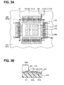
- FIG. 3A illustrates, of a printed board, vicinities of a surface-mounted area, where the electronic component is mounted.
- FIG. 3B illustrates a cross-sectional view of the electronic device in a vicinity of the surface-mounted area.
- the electronic device is suitable, for instance, for an electronic control unit constituting a vehicular engine ECU (Electronic Control Unit).
- ECU Electronic Control Unit
- the electronic device 100 includes a housing 200 and a circuit board 300.
- the housing 200 is made of metal material (i.e., aluminum, iron) or synthetic resin material.
- the housing 200 includes (i) a case 210 shaped of a container with an opening and (ii) an approximately rectangular shallow-depth cover 220 sealing the opening of the case 210.
- the case 210 and cover 220 are packaged or assembled with each other to form the housing 200 while the circuit board 300 is contained in an internal space of the housing 200.
- the case 210 and cover 220 are fixedly screwed to each other.
- the housing 200 is not limited to the above structure, but may be constructed of one integrated member or three members.
- the circuit board 300 includes (i) a printed board 310, and (ii) components surface-mounted on the printed board 310.
- the printed board 310 includes lands 311, reinforcement lands 312, conductive wires 317 (i.e., electric wiring lines), inner layer wires 317d, via-holes 315a coupling wires (e.g., coupling a wire 317 with an inner layer wire 317d), and the like.
- the mounted components include (i) electronic components 320 such as a microcomputer, a power transistor, a resistance, and a capacitor, and (ii) a connector 330 as an external connection terminal (i.e., an input/output unit).
- Material of the printed board 310 may be thermo-plastic resin, thermoset resin, ceramic, or a complex of glass (e.g., glass cloth) and resin, all of which are known.
- a resist 316 is formed on a surface of the printed board 310.
- the connector 330 includes (i) terminals 331 made of conductive material and (ii) a connector housing 332 containing the terminals 331. Of each of the terminals 331, one end is mounted on the printed board 310, while the other end is exposed from the housing 200.
- the housing 200 has a cut portion (not shown). Through the cut portion, a portion of the connector 330 enters an inside of the housing 200.
- the case 210 and cover 220 are fixedly screwed to each other to contain the circuit board 300. The other remaining portion of the connector 330 is exposed from the housing 200.
- Multiple terminals 331 are punched terminals, which are formed by punching a metal plate, and partially embedded within the connector housing 332 such that individual terminals do not interfere with each other.
- one connector housing 332 has multiple terminals 331 arranged in a row. The connection portions of the terminals 331 are arranged in a row with respect to the printed board 310.
- the terminals 331 may be differently arranged without limited to the above structure.
- one electronic component 320 is a QFN (Quad Flat Non-Leaded Package) 320a of a surface-mounted type shown in FIG. 2.
- the QFN 320a shaped of a rectangular parallelepiped, includes a reinforcement portion 321, an adhesive 322, an IC chip 323, multiple terminal portions 324, multiple leads 325, and a main body 326.
- the IC chip 323 is connected to the reinforcement portion 321 via the adhesive 322.
- An electrode (not shown) of the IC chip 323 is electrically coupled with the terminal portion 324 by the lead 325.
- the main body 326 of the QFN 320a is formed by resin-molding the IC chip 323, the adhesive 322, part of the reinforcement portion 321, part of the terminal portions 324, and the leads 325.
- the other part of the reinforcement portion 321 and the other part of the terminal portions 324 are exposed from the main body 326.
- the reinforcement portion 321 is used for supporting connection with the printed board 310 and dissipating heat due to operation of the QFN 320a or IC chip 323 towards the printed board 310.
- the mounted area 400 which is approximately rectangular, is illustrated in FIG. 3A to be surrounded by a chain double-dashed line.
- the printed board 310 includes multiple lands 311, multiple wires 317, and reinforcement lands 312.
- the lands 311 are made of conductive members such as copper foil and arranged to adjoin to each other with intervals while individually corresponding to terminal portions 324 exposed from the main body 326 of the QFN 320a. For instance, the lands are arranged to cross peripheral lines of the mounted area 400, as shown in FIG. 3A.
- One wire 317 corresponds to and is electrically connected with one land 311 as shown in FIG. 3B.
- the wire 317 has a via-hole connection portion 317e, which is electrically coupled with an inner layer wire 317d via a via-hole 315a.
- the via-hole 315a is a hole, which is formed in the printed board 310 with a laser or the like and filled with conductive pastes.
- the width of the via-hole connection portion 317e is larger than that of the wire 317 to secure connection reliability.
- the diameter of the via-hole connection portion 317e is larger than the width of the wire 317.
- the wire 317 is provided with a resist 314 thereon to prevent unintentional electrical connection with an adjacent wire 317.
- a via-hole portion 315 is defined as a combination of the via-hole connection portion 317e, the via-hole 315a, and a resist, which is provided to the via-hole connection portion 317e.
- the via-hole portion 315 has a shape meeting the diameter of the via-hole connection portion 317e.
- the wire 317 may be integrated with the land 311 or separated from the land 311.
- the reinforcement lands 312 and the solder resist 313 function as a connection member, which is coupled with the reinforcement portion 321 of the QFN 320a with solder 318.
- the reinforcement land 312 is used for supporting connection with the QFN 320a and dissipating heat due to operation of the QFN 320a or IC chip 323 towards the printed board 310.
- the reinforcement land 312 is made of conductive material such as copper foil similarly with the land 311.
- a solder resist 313 is provided to surround the reinforcement land 312 and electrically isolate the reinforcement land 312 from an outside thereof. When the reinforcement land 312 is electrically coupled with the ground potential, radiating noises from the IC chip 323 may be suitably decreased.
- the printed board 310 includes the multiple lands 311, the multiple reinforcement lands 312, and the multiple wires 317.
- the QFN 320a includes the multiple terminal portions 324 and the reinforcement portion 321.
- the multiple terminal portions 324 of the QFN 320a are electrically coupled with the lands 311 of the printed board 310 and the reinforcement portion 321 of the QFN 320a is surface-mounted to be mechanically coupled with the reinforcement lands in the printed board 310 with solder 318.
- the multiple wire 317 include at least first inside wires 317a, which are arranged within the mounted area 400 surrounded by a chain double-dashed line in FIG. 3A.
- the mounted area 400 is an area where the printed board 310 faces the QFN 320a.
- an inside wire 317a is defined as a wire arranged inside of the mounted area 400 and an outside wire 317b is defined as a wire arranged outside of the mounted area 400.
- the inside wires 317a and the outside wires 317b are alternately arranged along a peripheral line or side of the mounted area 400, as shown in FIG. 3A. Alternate arrangement of the inside and outside wires 317a, 317b allows a relatively large interval between adjacent wires 317.
- a bypass capacitor 320b for decreasing noises is electrically mounted.
- the bypass capacitor 320b is electrically mounted to bridge the adjacent outside wires 317b.
- the reinforcement lands 312 and the solder resist 313 as the connection member are arranged within the mounted area 400 to receive the inside wires 317a.
- both the connection member 312, 313 and the inside wires 317a co-exist without interfering each other.
- the reinforcement lands 312 and the solder resist 313 are arranged to face the inside wires 317a with a predetermined interval.
- FIG. 10A illustrates a printed board 310 of the comparative example.
- FIG. 10B illustrates an enlarged view of the wires 317.
- a via-hole portion 315 is defined as a combination of a via-hole connection portion 317e, a via-hole 315a, and a resist, which is provided to the via-hole connection portion 317e.
- the adjacent via-hole portions 315 need to be separated from each other.
- the via-hole portion 315 and the wire 317 also need to be separated from each other.
- individual via-holes 315a are arranged in a zigzag pattern or staggered pattern, and wires 317 need to have two different lengths (x1, x2) to correspond to the via-holes arranged in the zigzag pattern.
- wires 317 include two types of wires with a length of x1 from a land 311 and wires with a length of x2 from a land 311.
- wires 317 are arranged both inside of the mounted area 400 and outside of the mounted area 400.
- an interval between adjacent wires can be provided to be relatively larger.
- lengths of the wires can be an identical length, e.g., x1 from a land 311.
- the electronic device 100 of this embodiment can provide, outside the mounted area 400, an additional mounted area corresponding to the inside wires 317a arranged inside of the mounted area 400 and the differences of (x2 - x1).
- At least part (i.e., inside wire 317a) of wires 317 are arranged within the mounted area 400.
- the reinforce lands 312 and the solder resist 313 are designed to be arranged such that the inside wires 317a are also accommodated within the mounted area 400.
- This layout of the printed board 310 secures an additional area surrounding the mounted area 400 (or the mounted QFN 320a) for another component to be mounted. This enhances a mounting efficiency in the printed board 310.
- An electronic device such as an engine ECU has been recently required to be multi-functional and small-sized.
- the electronic device 100 of this embodiment capable of enhancing the mounting efficiency in the printed board 310 is suitably applied to an engine ECU.
- Securing an area surrounding the QFN 320a allows a noise-decrease elemental component such as a bypass capacitor 320b to be mounted in proximity of the electronic component (i.e., QFN 320a). This decreases conductive noises.
- a noise-decrease elemental component such as a bypass capacitor 320b
- a QFN 320a is applied as an electronic component; however, another component can be also applied.
- Requirements for this component are as follows: (i) terminal portions exposed from a main body of the electronic component are electrically coupled with lands in a printed board, and (ii) the main body is mechanically coupled with a surface of the main body, which the printed board faces, (i.e., the main body is mechanically coupled with at least a part of a mounted area in a printed board).
- FIG. 4 illustrates a printed board 310 of an electronic device as a modification 1.
- a modified part is mainly explained below.
- the different features are layouts of inside wires 317a, reinforcement lands 312, and solder resist 313.
- Adjacent lands can be sequentially coupled only with inside wires 317a without being coupled with outside wires 317b. With reference to Area B in FIG. 4, adjacent multiple lands 311 are connected only with inside wires 317a instead of being connected with outside wires.
- connection member i.e., the reinforcement lands 312 and solder resist 313
- the connection member further includes four protruding portions partially protruding towards an area, where few inside wires 317a are arranged, so as to secure strength of connection between the QFN 320a and the printed board 310.
- arranging multiple inside wires 317 serially coupled with adjacent lands 311 within the mounted area 400 allows a relatively large area to be secured in a peripheral area surrounding the QFN 320a.
- a relatively large-sized elemental component 320c can be arranged in proximity of the QFN 320a. This enhances a mounting efficiency in the printed board 310.
- FIG. 5 illustrates a printed board 310 of an electronic device as a modification 2.
- a modified part is mainly explained below.
- the different features are layouts of inside wires 317a.
- all wires 317 can be provided as inside wires 317a, which are arranged within the mounted area 400, where the main body 326 is mounted.
- arranging all the wires 317 as inside wires 317a within the mounted area 400 allows a relatively large area to be secured in a peripheral area surrounding the QFN 320a. As a result, this enhances a mounting efficiency in the printed board 310.
- FIG. 6 illustrate a printed board 310 of an electronic device as a modification 3.
- connection member i.e., reinforcement lands 312 and solder resists 313
- the connection member may be provided as four corner connection sub-members, which are arranged closely to four corners of the approximately rectangular mounted area 400.
- wires 317 corresponding to lands arranged around the four corners of the mounted area 400 are arranged as corner outside wires 317b, which are shown in Area C in FIG. 6.
- each pair of a reinforcement land 312 and solder resist 313, as one corner connection sub-member is located closely to lands around one corner of the mounted area 400 without any inside wire intervening; further, the lands around the one corner are coupled with the corner outside wires 317b outside of the mounted area 400.
- a stress is apt to be applied to four corners. Therefore, arranging the reinforcement lands 312 and solder resists 313 to correspond to the four corners of the reinforcement portion 321 secures a strength in connection with the QFN 320a. Further, arranging wires 317 corresponding to lands around the four corners of the mounted area 400 as the corner outside wires 317b allows arrangement of the reinforcement lands 312 and solder resists 313 to correspond to the four corners of the reinforcement portion 321.
- FIG. 7 illustrates a printed board 310 of an electronic device as a modification 4.
- a modified part is mainly explained below.
- the different features are layouts of wires 317, reinforcement lands 312, and solder resist 313.
- connection member i.e., reinforcement lands 312 and solder resists 313 further includes a central connection sub-member, which is arranged in a central area (i.e., Area D in FIG. 7) within the mounted area 400, in addition to the four corner connection sub-members, which correspond to the four corners of the reinforcement portion 321.
- wires corresponding to lands arranged around four corners of the mounted area 400 are provided as the corner outside wires 317b; namely, no inside wires is provided in an area corresponding to the four corners of the reinforcement portion 321 of the QFN 320a.
- the other wires are provided as inside wires 317a.
- the reinforcement lands 312 of the central connection sub-member arranged in Area D may be electrically coupled with the ground. This structure helps decrease radiation noises of the IC chip 323 and exogenous noises.
- FIG. 8 illustrates a printed board 310 of an electronic device as a modification 5.
- a modified part is mainly explained below.
- the different features are layouts of wires 317.
- each of eight wider large-current wire 317L is arranged to connected to at least two lands 311 around a corner of the mounted area 400 for large current to flow.
- a corresponding resist 314L and a via-hole portion 315L are also illustrated.
- the large-current wire 317L needs many via-holes, which are not easily arranged within the mounted area 400.
- reinforcement lands 312 and solder resists 313 are arranged to correspond to the four corners of the reinforcement portion 321, lands around the corners of the mounted area 400 are required to be connected with the corner outside wires 317b. Therefore, the corner outside wires 317b coupled with the lands 311 around the corners are suitably used for a large-current wire.
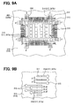
- FIG. 9A illustrates a printed board 310 of an electronic device as a modification 6.
- FIG. 9B illustrates an enlarged view of wires 317.
- the different feature is an interval between wires.
- wires corresponding to lands arranged around the four corners of the mounted area 400 are arranged as corner outside wires 317b; the other wires are provided as inside wires 317a.
- an interval y1 between the corner outside wires 317b (in Area F) is designed to be larger than an interval y2 between the inside wires 317a.
- lands 311 are alternately coupled with wires, i.e., wires 317b are coupled with every other land 311. Therefore, a land 311 not coupled with a wire is present.
- Designing an interval y1 between the corner outside wires 317b (in Area F) as being larger than an interval y2 between the inside wires 317a eliminates necessity of designing two different lengths of wires to correspond to via-holes 315a in a zigzag pattern in FIG. 10B or Area C in FIG 6.
Landscapes
- Engineering & Computer Science (AREA)
- Microelectronics & Electronic Packaging (AREA)
- Manufacturing & Machinery (AREA)
- Structure Of Printed Boards (AREA)
- Structures For Mounting Electric Components On Printed Circuit Boards (AREA)
- Multi-Conductor Connections (AREA)
Applications Claiming Priority (1)
| Application Number | Priority Date | Filing Date | Title |
|---|---|---|---|
| JP2006051181A JP4770514B2 (ja) | 2006-02-27 | 2006-02-27 | 電子装置 |
Publications (2)
| Publication Number | Publication Date |
|---|---|
| EP1827062A2 true EP1827062A2 (de) | 2007-08-29 |
| EP1827062A3 EP1827062A3 (de) | 2008-08-20 |
Family
ID=38066651
Family Applications (1)
| Application Number | Title | Priority Date | Filing Date |
|---|---|---|---|
| EP07002932A Ceased EP1827062A3 (de) | 2006-02-27 | 2007-02-12 | Elektronische Vorrichtung |
Country Status (3)
| Country | Link |
|---|---|
| US (1) | US20070201215A1 (de) |
| EP (1) | EP1827062A3 (de) |
| JP (1) | JP4770514B2 (de) |
Cited By (1)
| Publication number | Priority date | Publication date | Assignee | Title |
|---|---|---|---|---|
| CN105529338A (zh) * | 2016-02-06 | 2016-04-27 | 京东方科技集团股份有限公司 | 阵列基板、覆晶薄膜、显示面板及显示装置 |
Families Citing this family (2)
| Publication number | Priority date | Publication date | Assignee | Title |
|---|---|---|---|---|
| JP5113114B2 (ja) * | 2009-04-06 | 2013-01-09 | 新光電気工業株式会社 | 配線基板の製造方法及び配線基板 |
| CN104681544A (zh) * | 2013-12-03 | 2015-06-03 | 上海北京大学微电子研究院 | 多芯片qfn封装结构 |
Citations (5)
| Publication number | Priority date | Publication date | Assignee | Title |
|---|---|---|---|---|
| JPH06252326A (ja) * | 1993-02-25 | 1994-09-09 | Fujitsu Ten Ltd | 多端子部品、配線基板、多端子部品の実装構造 |
| US5877942A (en) | 1997-08-04 | 1999-03-02 | Qualcomm Incorporated | Circuit card assembly footprint providing reworkable interconnection paths for use with a surface mount device |
| US20020063315A1 (en) | 2000-11-30 | 2002-05-30 | Chien-Ping Huang | Quad flat non-leaded package and leadframe for the same |
| JP2002299529A (ja) | 2001-03-16 | 2002-10-11 | Lg Electron Inc | Ic放熱構造 |
| US6501160B1 (en) | 1999-01-29 | 2002-12-31 | Hitachi, Ltd. | Semiconductor device and a method of manufacturing the same and a mount structure |
Family Cites Families (42)
| Publication number | Priority date | Publication date | Assignee | Title |
|---|---|---|---|---|
| JPS5761853A (en) * | 1980-09-30 | 1982-04-14 | Mitsubishi Motors Corp | Oil pressure control device |
| DE3328736A1 (de) * | 1982-09-17 | 1984-03-22 | Control Data Corp., 55440 Minneapolis, Minn. | Schaltungsplatte |
| US4705917A (en) * | 1985-08-27 | 1987-11-10 | Hughes Aircraft Company | Microelectronic package |
| IL80038A (en) * | 1985-10-29 | 1995-01-24 | Hughes Aircraft Co | Raised mounting for leadless chip carrier |
| US5204615A (en) * | 1991-10-24 | 1993-04-20 | Interconnect Devices, Inc. | Module attachment for printed circuit board test fixtures |
| JP2783093B2 (ja) * | 1992-10-21 | 1998-08-06 | 日本電気株式会社 | プリント配線板 |
| KR100292036B1 (ko) * | 1993-08-27 | 2001-09-17 | 윤종용 | 반도체패키지의제조방법및그에 따른반도체패키지 |
| US5367763A (en) * | 1993-09-30 | 1994-11-29 | Atmel Corporation | TAB testing of area array interconnected chips |
| US5475569A (en) * | 1993-11-16 | 1995-12-12 | Intel Corporation | Method of testing fine pitch surface mount IC packages |
| JPH08288626A (ja) * | 1995-04-19 | 1996-11-01 | Canon Inc | Ic及びプリント配線基板 |
| US5808259A (en) * | 1995-07-31 | 1998-09-15 | Spinner; Howard | Thick film apparatus and method for customizing IC test PCB |
| JP3432982B2 (ja) * | 1995-12-13 | 2003-08-04 | 沖電気工業株式会社 | 表面実装型半導体装置の製造方法 |
| JP3593234B2 (ja) * | 1996-04-23 | 2004-11-24 | 日立電線株式会社 | 半導体装置用両面配線テープキャリアの製造方法 |
| SG60102A1 (en) * | 1996-08-13 | 1999-02-22 | Sony Corp | Lead frame semiconductor package having the same and method for manufacturing the same |
| JPH10145027A (ja) * | 1996-11-15 | 1998-05-29 | Fujitsu Ltd | 電子回路パッケージおよびプリント配線板並びに実装方法 |
| US6521845B1 (en) * | 1997-06-12 | 2003-02-18 | Intel Corporation | Thermal spreading enhancements for motherboards using PBGAs |
| JP3658162B2 (ja) * | 1997-11-28 | 2005-06-08 | 株式会社ルネサステクノロジ | 半導体装置 |
| SG77652A1 (en) * | 1998-03-18 | 2001-01-16 | Hitachi Cable | Semiconductor device lead-patterning substrate and electronics device and method for fabricating same |
| JP3062192B1 (ja) * | 1999-09-01 | 2000-07-10 | 松下電子工業株式会社 | リ―ドフレ―ムとそれを用いた樹脂封止型半導体装置の製造方法 |
| JP2001217355A (ja) * | 1999-11-25 | 2001-08-10 | Hitachi Ltd | 半導体装置 |
| JP3925032B2 (ja) * | 2000-03-14 | 2007-06-06 | 富士ゼロックス株式会社 | プリント配線基板 |
| JP2001284783A (ja) * | 2000-03-30 | 2001-10-12 | Shinko Electric Ind Co Ltd | 表面実装用基板及び表面実装構造 |
| JP3660861B2 (ja) * | 2000-08-18 | 2005-06-15 | 株式会社ルネサステクノロジ | 半導体装置の製造方法 |
| JP2002076534A (ja) * | 2000-08-31 | 2002-03-15 | Alps Electric Co Ltd | プリント基板への発熱部品の取付構造 |
| JP4085572B2 (ja) * | 2000-11-30 | 2008-05-14 | 日立電線株式会社 | 半導体装置及びその製造方法 |
| US6924548B2 (en) * | 2001-01-31 | 2005-08-02 | Hitachi, Ltd. | Semiconductor device and its manufacturing method with leads that have an inverted trapezoid-like section |
| JP4034073B2 (ja) * | 2001-05-11 | 2008-01-16 | 株式会社ルネサステクノロジ | 半導体装置の製造方法 |
| US6744135B2 (en) * | 2001-05-22 | 2004-06-01 | Hitachi, Ltd. | Electronic apparatus |
| JP3833124B2 (ja) * | 2002-02-19 | 2006-10-11 | セイコーインスツル株式会社 | 表示装置 |
| JP2003258149A (ja) * | 2002-02-28 | 2003-09-12 | Denso Corp | エリア配置型半導体装置の配線構造 |
| US6838751B2 (en) * | 2002-03-06 | 2005-01-04 | Freescale Semiconductor Inc. | Multi-row leadframe |
| AU2003235967A1 (en) * | 2002-04-30 | 2003-11-17 | Renesas Technology Corp. | Semiconductor device and electronic device |
| JP2004071670A (ja) * | 2002-08-02 | 2004-03-04 | Fuji Photo Film Co Ltd | Icパッケージ、接続構造、および電子機器 |
| US6879319B2 (en) * | 2002-10-25 | 2005-04-12 | Eastman Kodak Company | Integrated OLED display and touch screen |
| JP4137059B2 (ja) * | 2003-02-14 | 2008-08-20 | 株式会社ルネサステクノロジ | 電子装置および半導体装置 |
| JP2004363365A (ja) * | 2003-06-05 | 2004-12-24 | Renesas Technology Corp | 半導体装置及びその製造方法 |
| CN100413070C (zh) * | 2004-01-30 | 2008-08-20 | 松下电器产业株式会社 | 部件内置模块、配备部件内置模块的电子设备以及部件内置模块的制造方法 |
| KR101088338B1 (ko) * | 2004-02-04 | 2011-11-30 | 이비덴 가부시키가이샤 | 다층프린트배선판 |
| JP2005310837A (ja) * | 2004-04-16 | 2005-11-04 | Elpida Memory Inc | 半導体装置及びその製造方法 |
| JP2006059928A (ja) * | 2004-08-18 | 2006-03-02 | Orion Denki Kk | プリント基板 |
| JP2006190771A (ja) * | 2005-01-05 | 2006-07-20 | Renesas Technology Corp | 半導体装置 |
| KR100648040B1 (ko) * | 2005-11-25 | 2006-11-23 | 삼성전자주식회사 | 다수의 금속 랜드를 가지는 인터포저 기판, 및 이로부터제작되는 인터포저를 포함하는 적층 칩 패키지 |
-
2006
- 2006-02-27 JP JP2006051181A patent/JP4770514B2/ja not_active Expired - Fee Related
-
2007
- 2007-02-08 US US11/703,660 patent/US20070201215A1/en not_active Abandoned
- 2007-02-12 EP EP07002932A patent/EP1827062A3/de not_active Ceased
Patent Citations (6)
| Publication number | Priority date | Publication date | Assignee | Title |
|---|---|---|---|---|
| JPH06252326A (ja) * | 1993-02-25 | 1994-09-09 | Fujitsu Ten Ltd | 多端子部品、配線基板、多端子部品の実装構造 |
| US5877942A (en) | 1997-08-04 | 1999-03-02 | Qualcomm Incorporated | Circuit card assembly footprint providing reworkable interconnection paths for use with a surface mount device |
| US6501160B1 (en) | 1999-01-29 | 2002-12-31 | Hitachi, Ltd. | Semiconductor device and a method of manufacturing the same and a mount structure |
| US20020063315A1 (en) | 2000-11-30 | 2002-05-30 | Chien-Ping Huang | Quad flat non-leaded package and leadframe for the same |
| JP2002299529A (ja) | 2001-03-16 | 2002-10-11 | Lg Electron Inc | Ic放熱構造 |
| US6728106B2 (en) | 2001-03-16 | 2004-04-27 | Lg Electronics, Inc. | Heat dissipation structure of integrated circuit (IC) |
Cited By (2)
| Publication number | Priority date | Publication date | Assignee | Title |
|---|---|---|---|---|
| CN105529338A (zh) * | 2016-02-06 | 2016-04-27 | 京东方科技集团股份有限公司 | 阵列基板、覆晶薄膜、显示面板及显示装置 |
| US10784187B2 (en) | 2016-02-06 | 2020-09-22 | Boe Technology Group Co., Ltd. | Array substrate, chip on film, display panel and display device |
Also Published As
| Publication number | Publication date |
|---|---|
| EP1827062A3 (de) | 2008-08-20 |
| JP4770514B2 (ja) | 2011-09-14 |
| JP2007234674A (ja) | 2007-09-13 |
| US20070201215A1 (en) | 2007-08-30 |
Similar Documents
| Publication | Publication Date | Title |
|---|---|---|
| CN1282244C (zh) | 具有三维载体安装集成电路封装阵列的电子模块 | |
| US8593825B2 (en) | Apparatus and method for vertically-structured passive components | |
| US11175030B2 (en) | LED lighting device | |
| US8624367B2 (en) | Semiconductor device including semiconductor chip mounted on lead frame | |
| US9906157B2 (en) | Package assembly | |
| US11450451B2 (en) | Circuit module and interposer | |
| CN207884978U (zh) | 元器件模块 | |
| US20010053070A1 (en) | Electronic unit equipped with electromagnetic shielding plate | |
| WO2008055134A2 (en) | Electronic device with inductor and integrated componentry | |
| EP1827062A2 (de) | Elektronische Vorrichtung | |
| CN106961793A (zh) | 电子模块及其形成封装结构的方法 | |
| US6574116B2 (en) | Inverter capacitor module and inverter | |
| JPH11243175A (ja) | 複合半導体装置 | |
| US6734546B2 (en) | Micro grid array semiconductor die package | |
| US8222719B2 (en) | Quad flat no lead (QFN) integrated circuit (IC) package having a modified paddle and method for designing the package | |
| JP2005166892A (ja) | スタック型小型メモリカード | |
| CN115250571B (zh) | 一种电子模块 | |
| US8503188B2 (en) | Mountable electronic circuit module | |
| CN213340772U (zh) | 导电端子以及电子装置 | |
| JP4545537B2 (ja) | 半導体装置及び半導体装置ユニット | |
| JPH06224369A (ja) | 半導体装置 | |
| KR20060127603A (ko) | 접지 프레임을 갖는 리드 프레임 타입 패키지 및 그를이용한 적층 패키지 | |
| JP3932907B2 (ja) | モジュール基板 | |
| JP2007234675A (ja) | 電子装置 | |
| JPH09205162A (ja) | プリント配線基板モジュール |
Legal Events
| Date | Code | Title | Description |
|---|---|---|---|
| PUAI | Public reference made under article 153(3) epc to a published international application that has entered the european phase |
Free format text: ORIGINAL CODE: 0009012 |
|
| AK | Designated contracting states |
Kind code of ref document: A2 Designated state(s): AT BE BG CH CY CZ DE DK EE ES FI FR GB GR HU IE IS IT LI LT LU LV MC NL PL PT RO SE SI SK TR |
|
| AX | Request for extension of the european patent |
Extension state: AL BA HR MK YU |
|
| PUAL | Search report despatched |
Free format text: ORIGINAL CODE: 0009013 |
|
| AK | Designated contracting states |
Kind code of ref document: A3 Designated state(s): AT BE BG CH CY CZ DE DK EE ES FI FR GB GR HU IE IS IT LI LT LU LV MC NL PL PT RO SE SI SK TR |
|
| AX | Request for extension of the european patent |
Extension state: AL BA HR MK RS |
|
| 17P | Request for examination filed |
Effective date: 20090220 |
|
| AKX | Designation fees paid |
Designated state(s): DE FR IT |
|
| 17Q | First examination report despatched |
Effective date: 20121108 |
|
| STAA | Information on the status of an ep patent application or granted ep patent |
Free format text: STATUS: THE APPLICATION HAS BEEN REFUSED |
|
| 18R | Application refused |
Effective date: 20150923 |