EP1774572B1 - Verfahren zum ätzen einer schicht auf einem substrat - Google Patents
Verfahren zum ätzen einer schicht auf einem substrat Download PDFInfo
- Publication number
- EP1774572B1 EP1774572B1 EP05761141.0A EP05761141A EP1774572B1 EP 1774572 B1 EP1774572 B1 EP 1774572B1 EP 05761141 A EP05761141 A EP 05761141A EP 1774572 B1 EP1774572 B1 EP 1774572B1
- Authority
- EP
- European Patent Office
- Prior art keywords
- layer
- etching
- silicon
- substrate
- gas
- Prior art date
- Legal status (The legal status is an assumption and is not a legal conclusion. Google has not performed a legal analysis and makes no representation as to the accuracy of the status listed.)
- Expired - Fee Related
Links
- 238000005530 etching Methods 0.000 title claims description 69
- 238000000034 method Methods 0.000 title claims description 61
- 239000000758 substrate Substances 0.000 title claims description 32
- 239000010410 layer Substances 0.000 claims description 202
- XUIMIQQOPSSXEZ-UHFFFAOYSA-N Silicon Chemical compound [Si] XUIMIQQOPSSXEZ-UHFFFAOYSA-N 0.000 claims description 36
- 229910052710 silicon Inorganic materials 0.000 claims description 35
- 239000010703 silicon Substances 0.000 claims description 35
- 229910021420 polycrystalline silicon Inorganic materials 0.000 claims description 26
- 239000011241 protective layer Substances 0.000 claims description 20
- VYPSYNLAJGMNEJ-UHFFFAOYSA-N Silicium dioxide Chemical compound O=[Si]=O VYPSYNLAJGMNEJ-UHFFFAOYSA-N 0.000 claims description 13
- 238000009792 diffusion process Methods 0.000 claims description 10
- 230000004888 barrier function Effects 0.000 claims description 9
- YCKRFDGAMUMZLT-UHFFFAOYSA-N Fluorine atom Chemical compound [F] YCKRFDGAMUMZLT-UHFFFAOYSA-N 0.000 claims description 8
- 229910052731 fluorine Inorganic materials 0.000 claims description 8
- 239000011737 fluorine Substances 0.000 claims description 8
- 238000009413 insulation Methods 0.000 claims description 5
- 150000004767 nitrides Chemical class 0.000 claims description 3
- 239000000377 silicon dioxide Substances 0.000 claims description 3
- 238000006116 polymerization reaction Methods 0.000 claims description 2
- 229910006990 Si1-xGex Inorganic materials 0.000 claims 17
- 229910007020 Si1−xGex Inorganic materials 0.000 claims 17
- 229910014263 BrF3 Inorganic materials 0.000 claims 1
- 229910020323 ClF3 Inorganic materials 0.000 claims 1
- 229910052681 coesite Inorganic materials 0.000 claims 1
- 229910052906 cristobalite Inorganic materials 0.000 claims 1
- 229910052682 stishovite Inorganic materials 0.000 claims 1
- 229910052905 tridymite Inorganic materials 0.000 claims 1
- FQFKTKUFHWNTBN-UHFFFAOYSA-N trifluoro-$l^{3}-bromane Chemical compound FBr(F)F FQFKTKUFHWNTBN-UHFFFAOYSA-N 0.000 claims 1
- JOHWNGGYGAVMGU-UHFFFAOYSA-N trifluorochlorine Chemical compound FCl(F)F JOHWNGGYGAVMGU-UHFFFAOYSA-N 0.000 claims 1
- IGELFKKMDLGCJO-UHFFFAOYSA-N xenon difluoride Chemical compound F[Xe]F IGELFKKMDLGCJO-UHFFFAOYSA-N 0.000 claims 1
- 239000007789 gas Substances 0.000 description 23
- 229920005591 polysilicon Polymers 0.000 description 21
- 238000000151 deposition Methods 0.000 description 18
- 230000008021 deposition Effects 0.000 description 17
- KRHYYFGTRYWZRS-UHFFFAOYSA-N Fluorane Chemical compound F KRHYYFGTRYWZRS-UHFFFAOYSA-N 0.000 description 14
- 239000012071 phase Substances 0.000 description 11
- 229910045601 alloy Inorganic materials 0.000 description 10
- 239000000956 alloy Substances 0.000 description 10
- 238000004519 manufacturing process Methods 0.000 description 10
- 229910052732 germanium Inorganic materials 0.000 description 9
- GNPVGFCGXDBREM-UHFFFAOYSA-N germanium atom Chemical compound [Ge] GNPVGFCGXDBREM-UHFFFAOYSA-N 0.000 description 9
- 238000001020 plasma etching Methods 0.000 description 9
- 239000004065 semiconductor Substances 0.000 description 7
- 229910052814 silicon oxide Inorganic materials 0.000 description 7
- 230000008018 melting Effects 0.000 description 5
- 238000002844 melting Methods 0.000 description 5
- 239000007858 starting material Substances 0.000 description 5
- 230000000694 effects Effects 0.000 description 4
- 238000005516 engineering process Methods 0.000 description 4
- 239000000463 material Substances 0.000 description 4
- 229910052751 metal Inorganic materials 0.000 description 4
- 239000002184 metal Substances 0.000 description 4
- 229910021421 monocrystalline silicon Inorganic materials 0.000 description 4
- 238000002161 passivation Methods 0.000 description 4
- 229910000577 Silicon-germanium Inorganic materials 0.000 description 3
- 229920002120 photoresistant polymer Polymers 0.000 description 3
- 229920000642 polymer Polymers 0.000 description 3
- 229910052581 Si3N4 Inorganic materials 0.000 description 2
- LEVVHYCKPQWKOP-UHFFFAOYSA-N [Si].[Ge] Chemical compound [Si].[Ge] LEVVHYCKPQWKOP-UHFFFAOYSA-N 0.000 description 2
- QVGXLLKOCUKJST-UHFFFAOYSA-N atomic oxygen Chemical compound [O] QVGXLLKOCUKJST-UHFFFAOYSA-N 0.000 description 2
- 238000005137 deposition process Methods 0.000 description 2
- 238000002513 implantation Methods 0.000 description 2
- 239000001301 oxygen Substances 0.000 description 2
- 229910052760 oxygen Inorganic materials 0.000 description 2
- 230000001681 protective effect Effects 0.000 description 2
- HQVNEWCFYHHQES-UHFFFAOYSA-N silicon nitride Chemical compound N12[Si]34N5[Si]62N3[Si]51N64 HQVNEWCFYHHQES-UHFFFAOYSA-N 0.000 description 2
- 229910004298 SiO 2 Inorganic materials 0.000 description 1
- 239000004809 Teflon Substances 0.000 description 1
- 229920006362 Teflon® Polymers 0.000 description 1
- 229910001080 W alloy Inorganic materials 0.000 description 1
- 229910052782 aluminium Inorganic materials 0.000 description 1
- XAGFODPZIPBFFR-UHFFFAOYSA-N aluminium Chemical compound [Al] XAGFODPZIPBFFR-UHFFFAOYSA-N 0.000 description 1
- 238000000637 aluminium metallisation Methods 0.000 description 1
- 238000004873 anchoring Methods 0.000 description 1
- 238000004380 ashing Methods 0.000 description 1
- 230000009286 beneficial effect Effects 0.000 description 1
- 239000000919 ceramic Substances 0.000 description 1
- 239000004020 conductor Substances 0.000 description 1
- 238000005260 corrosion Methods 0.000 description 1
- 230000007797 corrosion Effects 0.000 description 1
- 230000007423 decrease Effects 0.000 description 1
- 230000001419 dependent effect Effects 0.000 description 1
- 238000007599 discharging Methods 0.000 description 1
- 239000002019 doping agent Substances 0.000 description 1
- 238000001312 dry etching Methods 0.000 description 1
- 238000001035 drying Methods 0.000 description 1
- 238000000407 epitaxy Methods 0.000 description 1
- 239000000945 filler Substances 0.000 description 1
- 239000010408 film Substances 0.000 description 1
- 239000011521 glass Substances 0.000 description 1
- 239000012212 insulator Substances 0.000 description 1
- 238000010849 ion bombardment Methods 0.000 description 1
- 230000000155 isotopic effect Effects 0.000 description 1
- 239000004922 lacquer Substances 0.000 description 1
- 230000002045 lasting effect Effects 0.000 description 1
- 239000003973 paint Substances 0.000 description 1
- 230000035515 penetration Effects 0.000 description 1
- RLOWWWKZYUNIDI-UHFFFAOYSA-N phosphinic chloride Chemical compound ClP=O RLOWWWKZYUNIDI-UHFFFAOYSA-N 0.000 description 1
- 239000010909 process residue Substances 0.000 description 1
- 238000000926 separation method Methods 0.000 description 1
- 235000012239 silicon dioxide Nutrition 0.000 description 1
- 239000010409 thin film Substances 0.000 description 1
- WFKWXMTUELFFGS-UHFFFAOYSA-N tungsten Chemical compound [W] WFKWXMTUELFFGS-UHFFFAOYSA-N 0.000 description 1
- 229910052721 tungsten Inorganic materials 0.000 description 1
- 239000010937 tungsten Substances 0.000 description 1
- 239000012808 vapor phase Substances 0.000 description 1
- 238000001039 wet etching Methods 0.000 description 1
Images
Classifications
-
- H—ELECTRICITY
- H01—ELECTRIC ELEMENTS
- H01L—SEMICONDUCTOR DEVICES NOT COVERED BY CLASS H10
- H01L21/00—Processes or apparatus adapted for the manufacture or treatment of semiconductor or solid state devices or of parts thereof
- H01L21/02—Manufacture or treatment of semiconductor devices or of parts thereof
- H01L21/04—Manufacture or treatment of semiconductor devices or of parts thereof the devices having potential barriers, e.g. a PN junction, depletion layer or carrier concentration layer
- H01L21/18—Manufacture or treatment of semiconductor devices or of parts thereof the devices having potential barriers, e.g. a PN junction, depletion layer or carrier concentration layer the devices having semiconductor bodies comprising elements of Group IV of the Periodic Table or AIIIBV compounds with or without impurities, e.g. doping materials
- H01L21/30—Treatment of semiconductor bodies using processes or apparatus not provided for in groups H01L21/20 - H01L21/26
- H01L21/31—Treatment of semiconductor bodies using processes or apparatus not provided for in groups H01L21/20 - H01L21/26 to form insulating layers thereon, e.g. for masking or by using photolithographic techniques; After treatment of these layers; Selection of materials for these layers
- H01L21/3205—Deposition of non-insulating-, e.g. conductive- or resistive-, layers on insulating layers; After-treatment of these layers
- H01L21/321—After treatment
- H01L21/3213—Physical or chemical etching of the layers, e.g. to produce a patterned layer from a pre-deposited extensive layer
- H01L21/32133—Physical or chemical etching of the layers, e.g. to produce a patterned layer from a pre-deposited extensive layer by chemical means only
- H01L21/32135—Physical or chemical etching of the layers, e.g. to produce a patterned layer from a pre-deposited extensive layer by chemical means only by vapour etching only
- H01L21/32136—Physical or chemical etching of the layers, e.g. to produce a patterned layer from a pre-deposited extensive layer by chemical means only by vapour etching only using plasmas
- H01L21/32137—Physical or chemical etching of the layers, e.g. to produce a patterned layer from a pre-deposited extensive layer by chemical means only by vapour etching only using plasmas of silicon-containing layers
-
- B—PERFORMING OPERATIONS; TRANSPORTING
- B81—MICROSTRUCTURAL TECHNOLOGY
- B81C—PROCESSES OR APPARATUS SPECIALLY ADAPTED FOR THE MANUFACTURE OR TREATMENT OF MICROSTRUCTURAL DEVICES OR SYSTEMS
- B81C1/00—Manufacture or treatment of devices or systems in or on a substrate
- B81C1/00436—Shaping materials, i.e. techniques for structuring the substrate or the layers on the substrate
- B81C1/00444—Surface micromachining, i.e. structuring layers on the substrate
- B81C1/00468—Releasing structures
- B81C1/00476—Releasing structures removing a sacrificial layer
-
- B—PERFORMING OPERATIONS; TRANSPORTING
- B81—MICROSTRUCTURAL TECHNOLOGY
- B81C—PROCESSES OR APPARATUS SPECIALLY ADAPTED FOR THE MANUFACTURE OR TREATMENT OF MICROSTRUCTURAL DEVICES OR SYSTEMS
- B81C1/00—Manufacture or treatment of devices or systems in or on a substrate
- B81C1/00436—Shaping materials, i.e. techniques for structuring the substrate or the layers on the substrate
- B81C1/00555—Achieving a desired geometry, i.e. controlling etch rates, anisotropy or selectivity
- B81C1/00595—Control etch selectivity
-
- H—ELECTRICITY
- H01—ELECTRIC ELEMENTS
- H01L—SEMICONDUCTOR DEVICES NOT COVERED BY CLASS H10
- H01L21/00—Processes or apparatus adapted for the manufacture or treatment of semiconductor or solid state devices or of parts thereof
- H01L21/02—Manufacture or treatment of semiconductor devices or of parts thereof
- H01L21/04—Manufacture or treatment of semiconductor devices or of parts thereof the devices having potential barriers, e.g. a PN junction, depletion layer or carrier concentration layer
- H01L21/18—Manufacture or treatment of semiconductor devices or of parts thereof the devices having potential barriers, e.g. a PN junction, depletion layer or carrier concentration layer the devices having semiconductor bodies comprising elements of Group IV of the Periodic Table or AIIIBV compounds with or without impurities, e.g. doping materials
- H01L21/30—Treatment of semiconductor bodies using processes or apparatus not provided for in groups H01L21/20 - H01L21/26
- H01L21/302—Treatment of semiconductor bodies using processes or apparatus not provided for in groups H01L21/20 - H01L21/26 to change their surface-physical characteristics or shape, e.g. etching, polishing, cutting
- H01L21/306—Chemical or electrical treatment, e.g. electrolytic etching
- H01L21/3065—Plasma etching; Reactive-ion etching
- H01L21/30655—Plasma etching; Reactive-ion etching comprising alternated and repeated etching and passivation steps, e.g. Bosch process
Definitions
- the present invention relates to a method for etching a layer to be removed on a substrate according to the preamble of claim 1 as shown in FIG US 2003/0215989 A1 known.
- the US 2002/0153808 A1 also discloses such a method of etching a layer to be removed on a substrate.
- a particular layer such as a sacrificial layer on a semiconductor substrate
- a sacrificial layer is formed on the substrate, on which a further structural layer is deposited and patterned.
- the sacrificial layer is selectively removed to expose the structures.
- the sacrificial layer can be removed dry or wet-chemically.
- a sensor and a method for producing a sensor are known, in which a thermal oxide is first deposited on a silicon substrate, on top of which a thin layer of heavily doped polysilicon for use as a buried interconnect is applied. Subsequently, a further oxide layer and, for example, a thick epipolysilicon layer are deposited on the polysilicon layer. This is followed by the deposition and structuring of a superficial aluminum metallization. Finally, the sensor structures to be exposed, preferably with a in the DE 42 41 045 C1 etched out etched fluorine-based Siliziumianaenharmtage.
- the exposure of the sensor element is done by means of a sacrificial layer etching in which the oxide is typically removed by hydrofluoric acid containing media via a Dampfsleyclar under the sensor areas.
- a disadvantage of this undercut technique is that the oxide is not only removed under the sensor area to be exposed, but also above and partially below the polysilicon interconnects, so that the risk of shunts and leakage currents exists.
- a protection of the oxide areas whose undercutting is to be prevented, for example by means of protective lacquers, is possible only with considerable effort, since vaporous hydrofluoric acid can penetrate almost all practicable polymeric protective layers very quickly and can also have a highly corrosive effect.
- an epi-polysilicon layer is deposited and by means of the in DE 42 41 045 C1 structured anisotropic deep etching process described.
- the thin oxide layer acts as a hard etch stop, which is subsequently itself removed by plasma etching with fluorine-rich etching gases such as CF 4 or C 2 F 6 under intense ion bombardment, ie under high substrate bias voltage.
- fluorine-rich etching gases such as CF 4 or C 2 F 6 under intense ion bombardment, ie under high substrate bias voltage.
- the side walls of the sensor structures are coated with a Teflon-type polymer or a Si oxide thin film as a protective layer, before the structure elements made of Epi polysilicon by isotropic gas phase undercutting z. B. with ClF 3 or by an isotropic fluorine plasma undercut are exposed. Because of the high selectivity of this etching step of at least 200-300: 1 with respect to silicon oxide, the oxide plane on the underside of the structural elements and optional
- the back oxide induces compressive stress and warpage of the structural members. This results in a lasting influence on the mechanical property of the structural elements by the oxide.
- the oxide plane should be as thin as possible, about 10 nm.
- the teflon-like or whatever protective layer on the structural sidewalls is often insufficient to avoid their etching attack during the isotropic gas phase or plasma etching step.
- Even an oxide layer instead of Teflon passivation which in a costly deposition process it is not enough to guarantee the necessary process safety. After exposing the sensor structure, this oxide layer is then to be removed again on the structure side walls, which is why the problematic effect of hydrofluoric acid or hydrofluoric acid vapor on the sensor structures is then finally applied.
- a method according to claims 1-15 is proposed.
- the inventive method according to claim 1 based on the fact that a layer of silicon-germanium alloy can be removed on a substrate in a gas phase etching with the aid of an etching gas, in particular highly selective to a substrate made of silicon.
- an etching gas in particular highly selective to a substrate made of silicon.
- CIF 3 a particularly advantageous etching gas.
- the etching behavior of the Si 1-x Ge x layer can be controlled via the Ge content in the alloy.
- a Si.sub.1 -x Ge.sub.x layer is used, in particular, as a sacrificial layer for producing a micromechanical sensor and the sacrificial layer is removed by gas phase etching, disadvantages described above relating to the removal of the sacrificial layer are avoided.
- the inventive method can completely dispense with an etching of a silicon oxide layer by hydrofluoric acid-containing media, so that an unwanted, but inevitable etching of protective layers does not take place above or below polysilicon interconnects. There is therefore no risk of shunts and leakage currents. Process reliability is also improved by the fact that there is no longer any dependence on sidewall protective layers, since in the etching method according to the invention a very high degree of stability is achieved Material-related selectivity of the structure to sacrificial layer is present.
- a Si 1-x Ge x layer may also be deposited as a fill layer on a substrate and removed by a gas phase etch in a simple manner to create a cavity after deposition of a capping layer on the substrate.
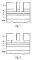
- FIG. 1 a micromechanical sensor element before and FIG. 2 after removal of the Si 1-x Ge x sacrificial layer in each case represents in section.
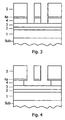
- FIGS. 3 and 4 show the FIGS. 3 and 4 a second possibility with respect to the layer structure of a sensor element, wherein FIG. 3 a micromechanical sensor element before and FIG. 4 after removal of the Si 1-x Ge x sacrificial layer in each case represents in section.
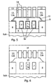
- FIGS. 5 and 6 a third possibility with respect to the layer structure of a sensor element, wherein FIG. 5 a micromechanical sensor element before and FIG. 6 after removal of the Si 1-x Ge x sacrificial and Si 1-x Ge x filling layer respectively in section represents. Description of the embodiments
- a first insulation layer typically a thick thermal insulation oxide
- a possible thickness of this oxide layer is in the range of a few micrometers, for example 2.5 microns.
- a conductive layer 2 preferably a thin polysilicon layer in a thickness of about 0.5 microns, applied.
- the insulating layer 1 may also consist of other oxides, silicon nitride or other insulating layers.
- Metallic layers are suitable for the conductive layer 2 in addition to polysilicon, if materials are chosen which are not critical for the subsequent high-temperature steps, such as tungsten or tungsten alloys.
- the conductive layer 2, which consists here of polysilicon as already mentioned, is doped by doping from the gas phase (POCl 3 ), whereby a high conductivity is sought. All other processes for producing a sufficiently heavily doped polysilicon layer can also be used.
- a structuring of the conductive layer 2 is then carried out by a photolithographic process.
- the conductive layer 2 is thus subdivided into individual mutually isolated regions, which can serve as printed conductors or electrodes, for example.
- a second insulating layer 3 is then deposited.
- the deposition processes known from semiconductor technology can be used for the deposition of dielectric layers.
- silicon dioxide it is thus also possible to deposit silicon nitride, various glasses or other ceramic layers.
- the second insulation layer 3 also consists of silicon oxide.
- a Si 1-x Ge x layer 4 is deposited on the second insulation layer 3 as a sacrificial layer.
- the thickness of the Si 1-x Ge x layer 4 is a few micrometers, for example 1.5 microns.
- a thick silicon layer 5 is applied to the Si 1-x Ge x layer 4.
- a polysilicon layer epitaxially, so-called. EpiPoly-Si, deposited.
- a polysilicon starter layer initially covers the surface of the Si 1-x Ge x layer 4 and serves as a seed for subsequent deposition.
- a corresponding doping process for example by implantation or by driving in dopants from the gas phase, any doping of the polysilicon starter layer that may be required can be ensured.
- all methods customary in semiconductor technology for the deposition of thin polysilicon layers are suitable.
- the deposition of the actual silicon layer 5 then takes place.
- This deposition takes place in an epitaxy reactor.
- Such an epitaxial reactor is a device for depositing silicon layers which are used in semiconductor technology for producing monocrystalline silicon layers on a monocrystalline silicon substrate. The deposition of such layers is usually carried out at temperatures of more than 1000 degrees Celsius and it can be achieved layer thicknesses of the order of a few 10 micrometers. Since the deposition in the epitaxial reactor is not carried out on a monocrystalline silicon substrate but on the polycrystalline silicon starting layer in the present process, no monocrystalline silicon layer is formed, but a thick polycrystalline silicon layer 5, so-called EpiPoly silicon, hereinafter referred to as thick silicon layer 5 referred to as.
- the crystalline properties of the thick silicon layer 5 can be influenced. Furthermore, the heavy doping of the polysilicon starter layer causes a doping of the thick silicon layer 5 starting from the underside. Furthermore, during the growth of the thick silicon layer 5 and in a subsequent doping process after growth, a further doping of the thick silicon layer 5 takes place. The subsequent doping of the thick silicon layer 5 can again be effected by implantation, doping from the gas phase or any other doping process known from semiconductor technology , The polysilicon starter layer becomes part of the thick silicon layer 5 in the process Figures 1 and 2 Not shown contact holes, the thick silicon layer 5 has a direct contact with the conductive layer 2.
- a metal layer is then applied and patterned, which in the Figures 1 and 2 have not been shown for reasons of clarity.
- the metal layer can for example be applied over the entire surface and then patterned.
- a mask for example a photomask
- a fluorine-based deep etching process is then carried out, for example, in separate etching steps and polymerization steps, each alternating successively, according to the teaching DE 42 41 045 C1 , With this deep etching process, trenches can be used a high aspect ratio, ie with great depth and small lateral dimension generated.
- the trenches extend from the top of the thick silicon layer 5 to the top of the second insulating layer 3.
- the silicon layer 5 is thus divided into individual regions which are insulated from each other, as long as they are not connected to one another via the conductive layer 2.
- an etching gas is then brought to the Si 1-x Ge x layer 4 according to the invention in a gas phase etching, the etching gas causing a highly selective etching of the Si 1-x Ge x layer 4.
- etching gas in addition to BrF 3 and XeF 2 preferably ClF 3 is used.
- ClF 3 as an etching gas in a layer to be removed from Si 1-x Ge x , the exceptionally high selectivity to epi-polysilicon about 4000: 1 and SiO 2 about 100000: 1.
- the etching behavior in particular the etching rate, can be controlled extremely effectively by the germanium content in the alloy.
- the substrate Sub After discharging from an etching system, the substrate Sub is freed from the photoresist mask and the remaining teflon-like sidewall films in an oxygen plasma stripper.
- This ashing process with an oxygen plasma is a well-known measure in the semiconductor industry for the removal of paint residues and process residues from previous plasma etching steps.
- a diffusion barrier 4a is provided between the Si 1-x Ge x layer 4 and the upper Si layer 5. Diffusion barrier 4a prevents outward diffusion of germanium into the upper Si layer 5.
- the diffusion barrier 4a is a thin Si oxide layer or a Si nitride layer having a thickness of only typically 10 to 100 nm. Such a thin layer of Si oxide or Si nitride is sufficient because it serves as a diffusion barrier here, but no passivation against an etching gas, especially ClF 3 , must ensure.
- the inventive method can be used in the Production of a micromechanical component having at least one cavity with a movable structure.
- a micromechanical component having at least one cavity with a movable structure.
- two Si 1-x Ge x layers each deposited as a sacrificial or filling layer in a region with sensor elements on a substrate and removed to produce a cavity after deposition of a cap layer on the substrate.
- a diffusion barrier 6a for germanium is deposited on the Si 1-x Ge x layer 6 from an oxide before the deposition of the silicon layer 7.
- the oxide layer has a thickness of only typically 10 to 100 nm. Because a passivation against an etching gas, in particular ClF 3 , does not have to ensure the diffusion barrier 6a. Only the passage of Ge atoms at the high temperature of subsequent process steps through the diffusion barrier in the form of the thin oxide layer and subsequent penetration into the silicon layer must be prevented, since this indiffusion would nullify the selectivity to Si 1-x Ge x layer 6.
- the protective layer 9 likewise has only a thickness of 10 to 100 nm, because here too it serves as a diffusion barrier against passage of germanium from Si 1-x Ge x layer into the adjacent Si layer, but no passivation with respect to an etching gas , in particular ClF 3 , must ensure.
- a covering of the first sacrificial layer by the first protective layer 9 can be omitted.
- Si 1-x Ge x layer 10 is applied to the structured sensor elements covered with the protective layer 9.
- This Si 1-x Ge x layer 10 serves as a second sacrificial layer and is a so-called filling layer.
- the thickness of the filling layer is chosen so that the later sensor elements are completely covered by it. Typically, the thickness of the filling layer is about 5 to 30 microns.
- a structuring of the filling layer is carried out such that the filling layer is left standing in those areas in which the later sensor elements are arranged. The filling layer is removed over the support structures 8 down to the silicon oxide protective layer 9.
- the second protective layer 11, like the first protective layer 9, can also be very thin. A thickness of about 10 to 100 nm is sufficient to out-diffuse To prevent germanium in the still applied, upper silicon layer 12.
- the second protective layer 11 is removed over the support structures 8 in regions such that the two protective layers 9, 11 on the support structures 8 merge into one another or lie sealingly on one another.
- a poly silicon layer 12 which serves as a cap layer 12a, is deposited on the second protective layer 11.
- the cap layer 12a is provided with a resist or oxide mask 13 and patterned with a Si deep etching process.
- the cap layer 12a is provided with perforation holes 14 which initially end on the second protective layer 11.
- a suitable etching medium can be supplied to the layers to be removed.
- both the filling layer and the first sacrificial layer of Si 1-x Ge x 6 are completely or at least partially removed from the sensor elements, so that a cavity 15 has formed, which has at least one movable sensor element 7a.
- the cover layer 16 is preferably between about 1 to 20 microns thick and consists for example of an insulator, preferably silica.
- a cavity 15 with movable sensor elements 7a on a substrate Sub is generated in a simple manner.
- the method can always be used to form a cavity 15 on a substrate, wherein the cavity 15 is produced by removing a filling layer of Si 1-x Ge x by means of an etching gas.
- the cavity 15 may have movable and / or non-movable sensor elements, or else serve other purposes without any sensor element.
- the proposed etching process can also always be used when a defined controllable etching of a layer or a substrate necessary or is desired.
- a layer or a substrate of silicon-germanium alloy is adjustable, wherein the content of germanium within the alloy in a certain direction, for example, over the thickness of the layer is varied in order to specifically produce a varying etching rate in gas phase etching.
- a layer sequence of several, individual layers with different Ge content is suitable to allow a selective etching. In extreme cases, an etching stop can thus be achieved.
Landscapes
- Engineering & Computer Science (AREA)
- Physics & Mathematics (AREA)
- Microelectronics & Electronic Packaging (AREA)
- Manufacturing & Machinery (AREA)
- Power Engineering (AREA)
- Plasma & Fusion (AREA)
- Condensed Matter Physics & Semiconductors (AREA)
- General Physics & Mathematics (AREA)
- Computer Hardware Design (AREA)
- Chemical & Material Sciences (AREA)
- Chemical Kinetics & Catalysis (AREA)
- General Chemical & Material Sciences (AREA)
- Geometry (AREA)
- Pressure Sensors (AREA)
- Micromachines (AREA)
- Investigating Or Analyzing Materials By The Use Of Fluid Adsorption Or Reactions (AREA)
- Drying Of Semiconductors (AREA)
Applications Claiming Priority (2)
| Application Number | Priority Date | Filing Date | Title |
|---|---|---|---|
| DE102004036803A DE102004036803A1 (de) | 2004-07-29 | 2004-07-29 | Verfahren zum Ätzen einer Schicht auf einem Substrat |
| PCT/EP2005/053121 WO2006013137A2 (de) | 2004-07-29 | 2005-07-01 | Verfahren zum ätzen einer sige-schicht auf einem substrat |
Publications (2)
| Publication Number | Publication Date |
|---|---|
| EP1774572A2 EP1774572A2 (de) | 2007-04-18 |
| EP1774572B1 true EP1774572B1 (de) | 2016-09-28 |
Family
ID=35124738
Family Applications (1)
| Application Number | Title | Priority Date | Filing Date |
|---|---|---|---|
| EP05761141.0A Expired - Fee Related EP1774572B1 (de) | 2004-07-29 | 2005-07-01 | Verfahren zum ätzen einer schicht auf einem substrat |
Country Status (6)
| Country | Link |
|---|---|
| US (1) | US8182707B2 (ko) |
| EP (1) | EP1774572B1 (ko) |
| JP (1) | JP4686544B2 (ko) |
| KR (1) | KR101130988B1 (ko) |
| DE (1) | DE102004036803A1 (ko) |
| WO (1) | WO2006013137A2 (ko) |
Families Citing this family (18)
| Publication number | Priority date | Publication date | Assignee | Title |
|---|---|---|---|---|
| DE10234589A1 (de) * | 2002-07-30 | 2004-02-12 | Robert Bosch Gmbh | Schichtsystem mit einer Siliziumschicht und einer Passivierschicht, Verfahren zur Erzeugung einer Passivierschicht auf einer Siliziumschicht und deren Verwendung |
| DE102005047081B4 (de) | 2005-09-30 | 2019-01-31 | Robert Bosch Gmbh | Verfahren zum plasmalosen Ätzen von Silizium mit dem Ätzgas ClF3 oder XeF2 |
| DE102006024668A1 (de) | 2006-05-26 | 2007-11-29 | Robert Bosch Gmbh | Mikromechanisches Bauelement und Verfahren zu dessen Herstellung |
| DE102006049259A1 (de) | 2006-10-19 | 2008-04-30 | Robert Bosch Gmbh | Verfahren zur Herstellung eines mikromechanischen Bauelementes mit einer Dünnschicht-Verkappung |
| DE102007033685A1 (de) | 2007-07-19 | 2009-01-22 | Robert Bosch Gmbh | Verfahren zum Ätzen einer Schicht auf einem Silizium-Halbleitersubstrat |
| DE102008042432A1 (de) | 2008-09-29 | 2010-04-01 | Robert Bosch Gmbh | Verfahren zur Herstellung eines Halbleiterbauelements |
| DE102010001420A1 (de) | 2010-02-01 | 2011-08-04 | Robert Bosch GmbH, 70469 | III-V-Halbleiter-Solarzelle |
| DE102010001504B4 (de) | 2010-02-02 | 2020-07-16 | Robert Bosch Gmbh | Eine Filtereinrichtung und ein Verfahren zur Herstellung einer Filtereinrichtung |
| JP5643635B2 (ja) * | 2010-12-24 | 2014-12-17 | 旭化成エレクトロニクス株式会社 | 半導体装置の製造方法 |
| KR20140022917A (ko) * | 2011-08-25 | 2014-02-25 | 다이니폰 스크린 세이조우 가부시키가이샤 | 패턴 형성 방법 |
| DE102011086610B4 (de) | 2011-11-18 | 2022-11-10 | Robert Bosch Gmbh | Verfahren zur Herstellung von Halbleiterstrukturen auf Siliziumcarbid-Basis |
| US9738516B2 (en) * | 2015-04-29 | 2017-08-22 | Taiwan Semiconductor Manufacturing Co., Ltd. | Structure to reduce backside silicon damage |
| JP6812880B2 (ja) * | 2017-03-29 | 2021-01-13 | 東京エレクトロン株式会社 | 基板処理方法及び記憶媒体。 |
| KR102390936B1 (ko) * | 2017-08-31 | 2022-04-26 | 구글 엘엘씨 | 양자 정보 처리 디바이스 형성 |
| DE102017120290B3 (de) * | 2017-09-04 | 2018-11-08 | Infineon Technologies Ag | Verfahren zum Prozessieren einer Schichtstruktur |
| CN109437093A (zh) * | 2018-10-26 | 2019-03-08 | 中国科学院苏州纳米技术与纳米仿生研究所 | 自支撑微纳米结构及其制作方法 |
| KR102599015B1 (ko) * | 2019-09-11 | 2023-11-06 | 주식회사 테스 | 기판 처리 방법 |
| US11791155B2 (en) * | 2020-08-27 | 2023-10-17 | Applied Materials, Inc. | Diffusion barriers for germanium |
Family Cites Families (22)
| Publication number | Priority date | Publication date | Assignee | Title |
|---|---|---|---|---|
| US3479680A (en) * | 1967-05-08 | 1969-11-25 | Stewart Warner Corp | Caster seal |
| JPH0192385A (ja) * | 1987-09-30 | 1989-04-11 | Iwatani Internatl Corp | 金属類物質又はその化合物を材質とする部材の微細加工方法 |
| JPH04208528A (ja) * | 1990-12-03 | 1992-07-30 | Nec Corp | 半導体装置の製造方法 |
| DE4241045C1 (de) | 1992-12-05 | 1994-05-26 | Bosch Gmbh Robert | Verfahren zum anisotropen Ätzen von Silicium |
| DE4420962C2 (de) | 1994-06-16 | 1998-09-17 | Bosch Gmbh Robert | Verfahren zur Bearbeitung von Silizium |
| DE19537814B4 (de) | 1995-10-11 | 2009-11-19 | Robert Bosch Gmbh | Sensor und Verfahren zur Herstellung eines Sensors |
| DE19847455A1 (de) * | 1998-10-15 | 2000-04-27 | Bosch Gmbh Robert | Verfahren zur Bearbeitung von Silizium mittels Ätzprozessen |
| DE10006035A1 (de) | 2000-02-10 | 2001-08-16 | Bosch Gmbh Robert | Verfahren zur Herstellung eines mikromechanischen Bauelements sowie ein nach dem Verfahren hergestelltes Bauelement |
| JP2002200599A (ja) | 2000-10-30 | 2002-07-16 | Sony Corp | 三次元構造体の作製方法 |
| FR2823032B1 (fr) * | 2001-04-03 | 2003-07-11 | St Microelectronics Sa | Resonateur electromecanique a poutre vibrante |
| KR100414217B1 (ko) * | 2001-04-12 | 2004-01-07 | 삼성전자주식회사 | 게이트 올 어라운드형 트랜지스터를 가진 반도체 장치 및그 형성 방법 |
| DE10142952A1 (de) * | 2001-06-13 | 2002-12-19 | Bosch Gmbh Robert | Herstellungsverfahren für eine mikromechanische Struktur |
| KR100446302B1 (ko) * | 2002-06-05 | 2004-08-30 | 삼성전자주식회사 | 음의 기울기를 가지는 게이트를 포함하는 반도체 소자 및그 제조방법 |
| JP3555682B2 (ja) * | 2002-07-09 | 2004-08-18 | セイコーエプソン株式会社 | 液体吐出ヘッド |
| JP4208528B2 (ja) | 2002-09-13 | 2009-01-14 | キヤノン株式会社 | 情報処理装置、機能拡張プログラム、それをコンピュータ読み取り可能に記憶した記憶媒体、情報処理方法 |
| KR100382245B1 (en) | 2002-12-12 | 2003-05-01 | Psk Inc | Asher equipment for semiconductor device manufacturing including cluster method |
| FR2849944B1 (fr) | 2003-01-14 | 2005-03-04 | Itt Mfg Enterprises Inc | Cadre pour le montage sur un panneau d'un connecteur pour carte a puce |
| DE10302676A1 (de) * | 2003-01-24 | 2004-07-29 | Robert Bosch Gmbh | Mikromechanisches Bauelement und Verfahren zu dessen Herstellung |
| US7078298B2 (en) * | 2003-05-20 | 2006-07-18 | Sharp Laboratories Of America, Inc. | Silicon-on-nothing fabrication process |
| US6936491B2 (en) | 2003-06-04 | 2005-08-30 | Robert Bosch Gmbh | Method of fabricating microelectromechanical systems and devices having trench isolated contacts |
| FR2857952B1 (fr) | 2003-07-25 | 2005-12-16 | St Microelectronics Sa | Resonateur electromecanique et procede de fabrication d'un tel resonateur |
| US7060539B2 (en) * | 2004-03-01 | 2006-06-13 | International Business Machines Corporation | Method of manufacture of FinFET devices with T-shaped fins and devices manufactured thereby |
-
2004
- 2004-07-29 DE DE102004036803A patent/DE102004036803A1/de not_active Ceased
-
2005
- 2005-07-01 KR KR1020077002100A patent/KR101130988B1/ko active IP Right Grant
- 2005-07-01 US US11/658,461 patent/US8182707B2/en active Active
- 2005-07-01 EP EP05761141.0A patent/EP1774572B1/de not_active Expired - Fee Related
- 2005-07-01 JP JP2007523054A patent/JP4686544B2/ja not_active Expired - Fee Related
- 2005-07-01 WO PCT/EP2005/053121 patent/WO2006013137A2/de active Application Filing
Also Published As
| Publication number | Publication date |
|---|---|
| JP4686544B2 (ja) | 2011-05-25 |
| KR20070046087A (ko) | 2007-05-02 |
| WO2006013137A2 (de) | 2006-02-09 |
| US8182707B2 (en) | 2012-05-22 |
| JP2008508704A (ja) | 2008-03-21 |
| KR101130988B1 (ko) | 2012-03-28 |
| EP1774572A2 (de) | 2007-04-18 |
| DE102004036803A1 (de) | 2006-03-23 |
| US20080311751A1 (en) | 2008-12-18 |
| WO2006013137A3 (de) | 2006-04-06 |
Similar Documents
| Publication | Publication Date | Title |
|---|---|---|
| EP1774572B1 (de) | Verfahren zum ätzen einer schicht auf einem substrat | |
| EP0000897B1 (de) | Verfahren zum Herstellen von lateral isolierten Siliciumbereichen | |
| DE10065013B4 (de) | Verfahren zum Herstellen eines mikromechanischen Bauelements | |
| DE10127231B4 (de) | Herstellungsverfahren eines Halbleitersubstrats | |
| DE10063991B4 (de) | Verfahren zur Herstellung von mikromechanischen Bauelementen | |
| DE4341271B4 (de) | Beschleunigungssensor aus kristallinem Material und Verfahren zur Herstellung dieses Beschleunigungssensors | |
| WO2000023376A1 (de) | Verfahren zur bearbeitung von silizium mittels ätzprozessen | |
| EP1169650B1 (de) | Unterschiedliche opferschichtdicken unter festen und beweglichen elektroden ( kapazitiver beschleunigungssensor ) | |
| EP2051929A1 (de) | Verfahren zur herstellung von mems-strukturen | |
| DE112007002739B4 (de) | Verfahren zur Herstellung eines Halbleiterbauelements mit Isolationsgraben und Kontaktgraben | |
| DE102019210285B4 (de) | Erzeugen eines vergrabenen Hohlraums in einem Halbleitersubstrat | |
| DE19817311B4 (de) | Herstellungsverfahren für mikromechanisches Bauelement | |
| DE102012222786A1 (de) | Verfahren zur fertigung einer halbleitervorrichtung | |
| DE10145724A1 (de) | Verfahren zum Herstellen einer Halbleiterstruktur unter Verwendung einer Schutzschicht und Halbleiterstruktur | |
| EP1360143B1 (de) | Verfahren zum erzeugen von oberflächenmikromechanikstrukturen und sensor | |
| DE102004015864B4 (de) | Verfahren zum Ausbilden von Seitenwandabstandhaltern | |
| EP1306348B1 (de) | Verfahren zur Herstellung einer Membransensoreinheit sowie Membransensoreinheit | |
| WO2003105220A1 (de) | Verfahren zur füllung von graben- und reliefgeometrien in halbleiterstrukturen | |
| WO1999049365A1 (de) | Verfahren zur herstellung grossflächiger membranmasken | |
| WO2006063885A1 (de) | Verfahren zum bilden eines grabens in einer mikrostruktur | |
| DE102006052630A1 (de) | Mikromechanisches Bauelement mit monolithisch integrierter Schaltung und Verfahren zur Herstellung eines Bauelements | |
| EP2217526B1 (de) | Verfahren zur herstellung von mikromechanischen strukturen mit reliefartigem seitenwandverlauf oder einstellbarem neigungswinkel | |
| EP1289876A1 (de) | Mikrostruktur und verfahren zu deren herstellung | |
| DE102009026639B4 (de) | Verfahren zum Herstellen einer elektromechanischen Mikrostruktur | |
| DE10046622A1 (de) | Verfahren zur Herstellung einer Membransensoreinheit sowie Membransensoreinheit |
Legal Events
| Date | Code | Title | Description |
|---|---|---|---|
| PUAI | Public reference made under article 153(3) epc to a published international application that has entered the european phase |
Free format text: ORIGINAL CODE: 0009012 |
|
| 17P | Request for examination filed |
Effective date: 20070228 |
|
| AK | Designated contracting states |
Kind code of ref document: A2 Designated state(s): AT BE BG CH CY CZ DE DK EE ES FI FR GB GR HU IE IS IT LI LT LU LV MC NL PL PT RO SE SI SK TR |
|
| R17P | Request for examination filed (corrected) |
Effective date: 20070228 |
|
| RBV | Designated contracting states (corrected) |
Designated state(s): DE FR IT |
|
| RIC1 | Information provided on ipc code assigned before grant |
Ipc: B81C 1/00 20060101ALI20070608BHEP Ipc: H01L 21/3213 20060101ALI20070608BHEP Ipc: B81B 3/00 20060101ALI20070608BHEP Ipc: H01L 21/3065 20060101AFI20070608BHEP |
|
| DAX | Request for extension of the european patent (deleted) | ||
| RBV | Designated contracting states (corrected) |
Designated state(s): DE FR IT |
|
| 17Q | First examination report despatched |
Effective date: 20151120 |
|
| GRAP | Despatch of communication of intention to grant a patent |
Free format text: ORIGINAL CODE: EPIDOSNIGR1 |
|
| INTG | Intention to grant announced |
Effective date: 20160704 |
|
| GRAS | Grant fee paid |
Free format text: ORIGINAL CODE: EPIDOSNIGR3 |
|
| GRAA | (expected) grant |
Free format text: ORIGINAL CODE: 0009210 |
|
| AK | Designated contracting states |
Kind code of ref document: B1 Designated state(s): DE FR IT |
|
| REG | Reference to a national code |
Ref country code: DE Ref legal event code: R096 Ref document number: 502005015381 Country of ref document: DE |
|
| REG | Reference to a national code |
Ref country code: DE Ref legal event code: R097 Ref document number: 502005015381 Country of ref document: DE |
|
| REG | Reference to a national code |
Ref country code: FR Ref legal event code: PLFP Year of fee payment: 13 |
|
| PLBE | No opposition filed within time limit |
Free format text: ORIGINAL CODE: 0009261 |
|
| STAA | Information on the status of an ep patent application or granted ep patent |
Free format text: STATUS: NO OPPOSITION FILED WITHIN TIME LIMIT |
|
| 26N | No opposition filed |
Effective date: 20170629 |
|
| REG | Reference to a national code |
Ref country code: FR Ref legal event code: PLFP Year of fee payment: 14 |
|
| REG | Reference to a national code |
Ref country code: DE Ref legal event code: R084 Ref document number: 502005015381 Country of ref document: DE |
|
| PGFP | Annual fee paid to national office [announced via postgrant information from national office to epo] |
Ref country code: FR Payment date: 20200727 Year of fee payment: 16 |
|
| PGFP | Annual fee paid to national office [announced via postgrant information from national office to epo] |
Ref country code: IT Payment date: 20200731 Year of fee payment: 16 |
|
| PG25 | Lapsed in a contracting state [announced via postgrant information from national office to epo] |
Ref country code: FR Free format text: LAPSE BECAUSE OF NON-PAYMENT OF DUE FEES Effective date: 20210731 |
|
| PG25 | Lapsed in a contracting state [announced via postgrant information from national office to epo] |
Ref country code: IT Free format text: LAPSE BECAUSE OF NON-PAYMENT OF DUE FEES Effective date: 20210701 |
|
| PGFP | Annual fee paid to national office [announced via postgrant information from national office to epo] |
Ref country code: DE Payment date: 20220927 Year of fee payment: 18 |
|
| REG | Reference to a national code |
Ref country code: DE Ref legal event code: R119 Ref document number: 502005015381 Country of ref document: DE |
|
| PG25 | Lapsed in a contracting state [announced via postgrant information from national office to epo] |
Ref country code: DE Free format text: LAPSE BECAUSE OF NON-PAYMENT OF DUE FEES Effective date: 20240201 |