EP1739726A1 - Bipolares halbleiterbauelement und prozess zu seiner herstellung - Google Patents
Bipolares halbleiterbauelement und prozess zu seiner herstellung Download PDFInfo
- Publication number
- EP1739726A1 EP1739726A1 EP05721512A EP05721512A EP1739726A1 EP 1739726 A1 EP1739726 A1 EP 1739726A1 EP 05721512 A EP05721512 A EP 05721512A EP 05721512 A EP05721512 A EP 05721512A EP 1739726 A1 EP1739726 A1 EP 1739726A1
- Authority
- EP
- European Patent Office
- Prior art keywords
- substrate
- silicon carbide
- sic
- epitaxial
- basal plane
- Prior art date
- Legal status (The legal status is an assumption and is not a legal conclusion. Google has not performed a legal analysis and makes no representation as to the accuracy of the status listed.)
- Withdrawn
Links
- 239000004065 semiconductor Substances 0.000 title claims abstract description 27
- 238000000034 method Methods 0.000 title claims abstract description 18
- 230000008569 process Effects 0.000 title claims abstract description 11
- 239000000758 substrate Substances 0.000 claims abstract description 126
- 229910010271 silicon carbide Inorganic materials 0.000 claims abstract description 121
- HBMJWWWQQXIZIP-UHFFFAOYSA-N silicon carbide Chemical compound [Si+]#[C-] HBMJWWWQQXIZIP-UHFFFAOYSA-N 0.000 claims abstract description 104
- UFHFLCQGNIYNRP-UHFFFAOYSA-N Hydrogen Chemical compound [H][H] UFHFLCQGNIYNRP-UHFFFAOYSA-N 0.000 claims abstract description 33
- 238000005530 etching Methods 0.000 claims abstract description 33
- 239000001257 hydrogen Substances 0.000 claims abstract description 30
- 229910052739 hydrogen Inorganic materials 0.000 claims abstract description 30
- 238000005498 polishing Methods 0.000 claims abstract description 29
- 239000000126 substance Substances 0.000 claims abstract description 16
- 238000004519 manufacturing process Methods 0.000 claims abstract description 12
- 239000013078 crystal Substances 0.000 claims description 39
- 230000003746 surface roughness Effects 0.000 claims description 15
- 238000011282 treatment Methods 0.000 description 29
- 238000003384 imaging method Methods 0.000 description 13
- 230000015556 catabolic process Effects 0.000 description 10
- 239000006061 abrasive grain Substances 0.000 description 9
- 230000000644 propagated effect Effects 0.000 description 9
- 238000005229 chemical vapour deposition Methods 0.000 description 8
- 238000006731 degradation reaction Methods 0.000 description 7
- VYPSYNLAJGMNEJ-UHFFFAOYSA-N Silicium dioxide Chemical compound O=[Si]=O VYPSYNLAJGMNEJ-UHFFFAOYSA-N 0.000 description 6
- 239000007789 gas Substances 0.000 description 6
- XLYOFNOQVPJJNP-UHFFFAOYSA-N water Substances O XLYOFNOQVPJJNP-UHFFFAOYSA-N 0.000 description 6
- 238000010438 heat treatment Methods 0.000 description 5
- 238000005130 seeded sublimation method Methods 0.000 description 5
- IJGRMHOSHXDMSA-UHFFFAOYSA-N Atomic nitrogen Chemical compound N#N IJGRMHOSHXDMSA-UHFFFAOYSA-N 0.000 description 4
- ATUOYWHBWRKTHZ-UHFFFAOYSA-N Propane Chemical compound CCC ATUOYWHBWRKTHZ-UHFFFAOYSA-N 0.000 description 4
- 238000001816 cooling Methods 0.000 description 4
- 238000001704 evaporation Methods 0.000 description 4
- 238000002347 injection Methods 0.000 description 4
- 239000007924 injection Substances 0.000 description 4
- 230000007774 longterm Effects 0.000 description 4
- 239000002002 slurry Substances 0.000 description 4
- 238000005092 sublimation method Methods 0.000 description 4
- 229910052782 aluminium Inorganic materials 0.000 description 3
- 239000012298 atmosphere Substances 0.000 description 3
- 229910052799 carbon Inorganic materials 0.000 description 3
- 238000006243 chemical reaction Methods 0.000 description 3
- 150000002500 ions Chemical class 0.000 description 3
- 239000000463 material Substances 0.000 description 3
- 229910052710 silicon Inorganic materials 0.000 description 3
- 238000004381 surface treatment Methods 0.000 description 3
- XKRFYHLGVUSROY-UHFFFAOYSA-N Argon Chemical compound [Ar] XKRFYHLGVUSROY-UHFFFAOYSA-N 0.000 description 2
- OKTJSMMVPCPJKN-UHFFFAOYSA-N Carbon Chemical compound [C] OKTJSMMVPCPJKN-UHFFFAOYSA-N 0.000 description 2
- BLRPTPMANUNPDV-UHFFFAOYSA-N Silane Chemical compound [SiH4] BLRPTPMANUNPDV-UHFFFAOYSA-N 0.000 description 2
- XUIMIQQOPSSXEZ-UHFFFAOYSA-N Silicon Chemical compound [Si] XUIMIQQOPSSXEZ-UHFFFAOYSA-N 0.000 description 2
- XAGFODPZIPBFFR-UHFFFAOYSA-N aluminium Chemical compound [Al] XAGFODPZIPBFFR-UHFFFAOYSA-N 0.000 description 2
- 230000004888 barrier function Effects 0.000 description 2
- 239000003795 chemical substances by application Substances 0.000 description 2
- 238000009792 diffusion process Methods 0.000 description 2
- 230000008020 evaporation Effects 0.000 description 2
- 230000005669 field effect Effects 0.000 description 2
- 230000006872 improvement Effects 0.000 description 2
- 229910052757 nitrogen Inorganic materials 0.000 description 2
- 239000001294 propane Substances 0.000 description 2
- 230000006798 recombination Effects 0.000 description 2
- 238000005215 recombination Methods 0.000 description 2
- 229910000077 silane Inorganic materials 0.000 description 2
- 239000010703 silicon Substances 0.000 description 2
- 239000000377 silicon dioxide Substances 0.000 description 2
- 239000010936 titanium Substances 0.000 description 2
- -1 Aluminum ions Chemical class 0.000 description 1
- VEXZGXHMUGYJMC-UHFFFAOYSA-N Hydrochloric acid Chemical compound Cl VEXZGXHMUGYJMC-UHFFFAOYSA-N 0.000 description 1
- RTAQQCXQSZGOHL-UHFFFAOYSA-N Titanium Chemical compound [Ti] RTAQQCXQSZGOHL-UHFFFAOYSA-N 0.000 description 1
- 230000009471 action Effects 0.000 description 1
- 238000013459 approach Methods 0.000 description 1
- 229910052786 argon Inorganic materials 0.000 description 1
- 239000012159 carrier gas Substances 0.000 description 1
- 239000008119 colloidal silica Substances 0.000 description 1
- 230000000593 degrading effect Effects 0.000 description 1
- 238000002050 diffraction method Methods 0.000 description 1
- 239000002019 doping agent Substances 0.000 description 1
- 230000000694 effects Effects 0.000 description 1
- 230000005684 electric field Effects 0.000 description 1
- 229910002804 graphite Inorganic materials 0.000 description 1
- 239000010439 graphite Substances 0.000 description 1
- 229910000041 hydrogen chloride Inorganic materials 0.000 description 1
- IXCSERBJSXMMFS-UHFFFAOYSA-N hydrogen chloride Substances Cl.Cl IXCSERBJSXMMFS-UHFFFAOYSA-N 0.000 description 1
- 239000012535 impurity Substances 0.000 description 1
- 230000006698 induction Effects 0.000 description 1
- 239000011810 insulating material Substances 0.000 description 1
- 230000003993 interaction Effects 0.000 description 1
- 238000005259 measurement Methods 0.000 description 1
- 229910044991 metal oxide Inorganic materials 0.000 description 1
- 150000004706 metal oxides Chemical class 0.000 description 1
- 238000012986 modification Methods 0.000 description 1
- 230000004048 modification Effects 0.000 description 1
- 230000002093 peripheral effect Effects 0.000 description 1
- 239000000843 powder Substances 0.000 description 1
- 239000010453 quartz Substances 0.000 description 1
- 239000012495 reaction gas Substances 0.000 description 1
- 230000036632 reaction speed Effects 0.000 description 1
- 230000009467 reduction Effects 0.000 description 1
- 239000002904 solvent Substances 0.000 description 1
- 238000000992 sputter etching Methods 0.000 description 1
- 238000012360 testing method Methods 0.000 description 1
- 229910052719 titanium Inorganic materials 0.000 description 1
- JLTRXTDYQLMHGR-UHFFFAOYSA-N trimethylaluminium Chemical compound C[Al](C)C JLTRXTDYQLMHGR-UHFFFAOYSA-N 0.000 description 1
- 238000009834 vaporization Methods 0.000 description 1
- 230000008016 vaporization Effects 0.000 description 1
Images
Classifications
-
- H—ELECTRICITY
- H01—ELECTRIC ELEMENTS
- H01L—SEMICONDUCTOR DEVICES NOT COVERED BY CLASS H10
- H01L29/00—Semiconductor devices specially adapted for rectifying, amplifying, oscillating or switching and having potential barriers; Capacitors or resistors having potential barriers, e.g. a PN-junction depletion layer or carrier concentration layer; Details of semiconductor bodies or of electrodes thereof ; Multistep manufacturing processes therefor
- H01L29/66—Types of semiconductor device ; Multistep manufacturing processes therefor
- H01L29/86—Types of semiconductor device ; Multistep manufacturing processes therefor controllable only by variation of the electric current supplied, or only the electric potential applied, to one or more of the electrodes carrying the current to be rectified, amplified, oscillated or switched
- H01L29/861—Diodes
- H01L29/8613—Mesa PN junction diodes
-
- H—ELECTRICITY
- H01—ELECTRIC ELEMENTS
- H01L—SEMICONDUCTOR DEVICES NOT COVERED BY CLASS H10
- H01L21/00—Processes or apparatus adapted for the manufacture or treatment of semiconductor or solid state devices or of parts thereof
- H01L21/02—Manufacture or treatment of semiconductor devices or of parts thereof
- H01L21/02002—Preparing wafers
- H01L21/02005—Preparing bulk and homogeneous wafers
- H01L21/02008—Multistep processes
- H01L21/0201—Specific process step
- H01L21/02019—Chemical etching
-
- H—ELECTRICITY
- H01—ELECTRIC ELEMENTS
- H01L—SEMICONDUCTOR DEVICES NOT COVERED BY CLASS H10
- H01L21/00—Processes or apparatus adapted for the manufacture or treatment of semiconductor or solid state devices or of parts thereof
- H01L21/02—Manufacture or treatment of semiconductor devices or of parts thereof
- H01L21/02002—Preparing wafers
- H01L21/02005—Preparing bulk and homogeneous wafers
- H01L21/02008—Multistep processes
- H01L21/0201—Specific process step
- H01L21/02024—Mirror polishing
-
- H—ELECTRICITY
- H01—ELECTRIC ELEMENTS
- H01L—SEMICONDUCTOR DEVICES NOT COVERED BY CLASS H10
- H01L21/00—Processes or apparatus adapted for the manufacture or treatment of semiconductor or solid state devices or of parts thereof
- H01L21/02—Manufacture or treatment of semiconductor devices or of parts thereof
- H01L21/02104—Forming layers
- H01L21/02365—Forming inorganic semiconducting materials on a substrate
- H01L21/02367—Substrates
- H01L21/0237—Materials
- H01L21/02373—Group 14 semiconducting materials
- H01L21/02378—Silicon carbide
-
- H—ELECTRICITY
- H01—ELECTRIC ELEMENTS
- H01L—SEMICONDUCTOR DEVICES NOT COVERED BY CLASS H10
- H01L21/00—Processes or apparatus adapted for the manufacture or treatment of semiconductor or solid state devices or of parts thereof
- H01L21/02—Manufacture or treatment of semiconductor devices or of parts thereof
- H01L21/02104—Forming layers
- H01L21/02365—Forming inorganic semiconducting materials on a substrate
- H01L21/02367—Substrates
- H01L21/02433—Crystal orientation
-
- H—ELECTRICITY
- H01—ELECTRIC ELEMENTS
- H01L—SEMICONDUCTOR DEVICES NOT COVERED BY CLASS H10
- H01L21/00—Processes or apparatus adapted for the manufacture or treatment of semiconductor or solid state devices or of parts thereof
- H01L21/02—Manufacture or treatment of semiconductor devices or of parts thereof
- H01L21/02104—Forming layers
- H01L21/02365—Forming inorganic semiconducting materials on a substrate
- H01L21/02518—Deposited layers
- H01L21/02521—Materials
- H01L21/02524—Group 14 semiconducting materials
- H01L21/02529—Silicon carbide
-
- H—ELECTRICITY
- H01—ELECTRIC ELEMENTS
- H01L—SEMICONDUCTOR DEVICES NOT COVERED BY CLASS H10
- H01L21/00—Processes or apparatus adapted for the manufacture or treatment of semiconductor or solid state devices or of parts thereof
- H01L21/02—Manufacture or treatment of semiconductor devices or of parts thereof
- H01L21/02104—Forming layers
- H01L21/02365—Forming inorganic semiconducting materials on a substrate
- H01L21/02612—Formation types
- H01L21/02617—Deposition types
- H01L21/0262—Reduction or decomposition of gaseous compounds, e.g. CVD
-
- H—ELECTRICITY
- H01—ELECTRIC ELEMENTS
- H01L—SEMICONDUCTOR DEVICES NOT COVERED BY CLASS H10
- H01L21/00—Processes or apparatus adapted for the manufacture or treatment of semiconductor or solid state devices or of parts thereof
- H01L21/02—Manufacture or treatment of semiconductor devices or of parts thereof
- H01L21/02104—Forming layers
- H01L21/02365—Forming inorganic semiconducting materials on a substrate
- H01L21/02656—Special treatments
- H01L21/02658—Pretreatments
- H01L21/02661—In-situ cleaning
Definitions
- the present invention relates to a bipolar type semiconductor device and its manufacturing process in which a region where an electron and a positive hole are recombined during current flowing, such as a drift layer, is formed with a silicon carbide epitaxial layer that has been grown from the surface of a silicon carbide substrate, in particular to a reduction of a basal plane dislocation density in the epitaxial layer and an improvement of a forward voltage degradation due to long-term operation.
- Silicon carbide is a semiconductor that has excellent material property values for a coefficient of thermal conductivity, electron mobility, and a band gap, in addition to the dielectric breakdown field strength of approximately ten times as strong as that of silicon (Si). Accordingly, silicon carbide is expected as a semiconductor material for implementing rapid performance improvement as compared with conventional Si power semiconductor devices. Recently, 4H-SiC and 6H-SiC monocrystal substrates with a diameter of up to three inches have been put on the market. In addition, many kinds of switching devices have been reported, such as a Schottky barrier diode (SBD), a high voltage pn diode, and a MOSFET that have a performance greatly exceeding the performance limit of Si. Thus high performance SiC devices are being developed.
- SBD Schottky barrier diode
- MOSFET MOSFET
- Semiconductor devices can be classified roughly into a unipolar device in which only an electron or a hole acts to conduction during current flowing and a bipolar device in which both an electron and a hole act to conduction during current flowing.
- a unipolar device devices such as a Schottky barrier diode (SBD), a junction field effect transistor (J-FET), and a metal oxide film semiconductor field effect transistor (MOS-FET) are given.
- the bipolar device devices such as a pn diode, a bipolar junction transistor (BJT), a thyristor, a GTO thyristor, and an IGBT are given.
- a conventional SiC bipolar device shows degradation due to long-term operation in which a forward voltage is increased corresponding to an increase in current flowing time (integrated usage time) after current flowing is started to a new bipolar device.
- a basal plane dislocation which is a kind of crystal faults.
- the basal plane dislocation is converted to a stacking fault by recombination energy of an electron and a hole that are generated during current flowing.
- An area of the stacking fault increases according to an increase in current flowing time. Since a region of the stacking fault acts as a high resistance region during current flowing, a forward voltage of a bipolar device is increased corresponding to an increase in an area of the stacking fault.
- a forward voltage is increased, a loss of an device increases, thus increasing a loss and degrading the reliability for a power conversion device such as an inverter using such an device.
- 3C-SiC, 4H-SiC, and 6H-SiC poly types of crystal are used in general.
- 4H-SiC is mainly used for developing power semiconductors since it has high dielectric breakdown strength, high mobility, and comparatively small anisotropy.
- the crystal plane in which the epitaxial growth is carried out is the (0001) Si plane, (000-1) C plane, (11-20) plane, (01-10) plane, or (03-38) plane, etc.
- the SiC monocrystal substrate that grows an epitaxial monocrystal film can be obtained by slicing a bulk crystal that has been formed by the sublimation method or the chemical vapor deposition (CVD) method, and by the mechanical polishing of the surface of the bulk crystal with polishing abrasive grains harder than or equivalent to SiC.
- a basal plane dislocation exists at a high density in the (0001) plane on the SiC monocrystal substrate that has been obtained by the sublimation method or the CVD method.
- a basal plane dislocation density on the surface of the substrate is in the range of 10 2 to 10 4 /cm 2 in general (the density depends on crystal quality).
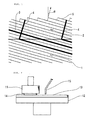
- a basal plane dislocation 3 on the surface of a substrate 1 are propagated to an epitaxial layer 2 as the basal plane dislocation 3 during an epitaxial growth, and the remainder of the basal plane dislocation 3 is converted to a threading edge dislocation 4 and propagated to the epitaxial layer 2.
- numeral 5 represents a (0001) Si plane and symbol ⁇ represents an off-angle.
- a region in which a basal plane dislocation is converted to a stacking fault during current flowing is a region in which an electron and a hole are recombined during current flowing.
- Most of the region in which an electron and a hole are recombined is a drift layer of a bipolar device, and a part of electrons and holes is penetrated to the injection layer side around the interface of the drift layer and the injection layer.
- Patent Document 1 International Patent Laid-Open Pamphlet WO03/038876
- Non-patent document 1 Materials Science Forum, 2002, Vol. 389 to 393, p. 1259 to 1264
- An object of the present invention is to provide a bipolar type semiconductor device and its manufacturing process in which a propagation of a basal plane dislocation from an SiC monocrystal substrate to an epitaxial layer can be reduced and thereby the degradation of a forward voltage due to long-term operation can be suppressed.
- the present inventor has carried out a hydrogen etching treatment to the surface of the SiC monocrystal substrate under the specified conditions before carrying out an epitaxial growth of SiC on the SiC monocrystal substrate.
- the present inventor has achieved the present invention by finding that a basal plane dislocation in the epitaxial film that has been grown from the treated surface is greatly reduced.
- the present inventor has treated the surface of the substrate by chemical mechanical polishing and then carried out a hydrogen etching treatment to the surface of the substrate.
- the present inventor has achieved the present invention by finding that a basal plane dislocation in the epitaxial film that has been grown from the treated surface by using the substrate with a low off-angle is greatly reduced.
- the basal plane dislocation can be greatly reduced.
- a bipolar type semiconductor device with relation to the present invention in which at least a part of a region where an electron and a hole are recombined during current flowing is formed with a silicon carbide epitaxial layer that has been grown from the surface of a silicon carbide substrate, is characterized by that a surface roughness Rms of the surface of the silicon carbide substrate on which an epitaxial growth is carried out is in the range of 0.1 to 0.6 nm.
- a bipolar type semiconductor device with relation to the present invention is characterized by that an off-angle of the silicon carbide substrate is in the range of 1 to 4°.
- a bipolar type semiconductor device with relation to the present invention is characterized by that a crystal plane of the silicon carbide substrate in which the epitaxial growth is carried out is the (000-1) C plane and an off-angle of the substrate is in the range of 1 to 8°.
- a process for manufacturing a bipolar type semiconductor device with relation to the present invention in which at least a part of a region where an electron and a hole are recombined during current flowing is formed with a silicon carbide epitaxial layer that has been grown from the surface of a silicon carbide substrate, is characterized by that the surface of the silicon carbide substrate is treated by hydrogen etching and the epitaxial layer is then formed by the epitaxial growth of silicon carbide from the treated surface.
- a process for manufacturing a bipolar type semiconductor device with relation to the present invention in which at least a part of a region where an electron and a hole are recombined during current flowing is formed with a silicon carbide epitaxial layer that has been grown from the surface of a silicon carbide substrate, is characterized by that the surface of the silicon carbide substrate is treated by chemical mechanical polishing and hydrogen etching in this order, and that the epitaxial layer is then formed by the epitaxial growth of silicon carbide from the treated surface.
- a process for manufacturing a bipolar type semiconductor device with relation to the present invention is characterized by that the epitaxial growth is carried out from the surface of the silicon carbide substrate with an off-angle in the range of 1 to 4°.
- a process for manufacturing a bipolar type semiconductor device with relation to the present invention is characterized by that the epitaxial growth is carried out from the (000-1) C plane of the silicon carbide substrate with an off-angle in the range of 1 to 8°.
- a basal plane dislocation in an epitaxial layer can be greatly reduced.
- the propagation of a basal plane dislocation from an SiC monocrystal substrate to an epitaxial layer can be greatly reduced.
- An SiC monocrystal substrate is formed by slicing a bulk crystal that has been obtained by the sublimation method or CVD method.
- SiC powder that has been put into a crucible is heated at the range of 2200 to 2400°C for vaporization, and is deposited on the surface of the seed crystal at a speed of the range of 0.8 to 1 mm per hour in general for bulk growth.
- the formed ingot is sliced at the specified thickness in such a manner that a desired crystal plane is exposed.
- the surface of the SiC monocrystal substrate is smoothed in the specular morphology by a treatment of polishing with abrasive grains harder than or equivalent to SiC, or the like. The rough abrasive grains are exchanged to fine abrasive grains as the polishing is progressed.
- a crystal type of SiC monocrystal such as 4H-SiC, 3C-SiC, 2H-SiC, 6H-SiC, and 15R-SiC can be used in general.
- 4H-SiC is preferably used in particular since it has high dielectric breakdown strength, high mobility, and comparatively small anisotropy.
- a basal plane dislocation density in an epitaxial layer can be greatly reduced by carrying out a hydrogen etching treatment or carrying out both the hydrogen etching treatment and chemical mechanical polishing treatment.
- the crystal plane in which the epitaxial growth is carried out is the (0001) Si plane, (000-1) C plane, (11-20) plane, (01-10) plane, or (03-38) plane, etc.
- a substrate is cut while being inclined at an off-angle of the range of 1 to 12°, preferably the range of 1 to 8°, particularly preferably the range of 1 to 4°, to the off-orientation of the [01-10] direction, the [11-20] direction, or a middle direction between the [01-10] direction and [11-20] direction, and the epitaxial growth from the crystal plane is carried out by the step flow growth technology.
- a propagation of a basal plane dislocation from the substrate to an epitaxial layer can be greatly reduced.
- the crystal plane of the substrate in which the epitaxial growth is carried out is the (000-1) C plane
- a propagation of a basal plane dislocation to an epitaxial layer can be greatly reduced even if the off-angle is comparatively larger than the range of 1 to 4°.
- the off-angle is in the range of 1 to 8°
- a propagation of a basal plane dislocation from the substrate to the epitaxial layer can be greatly reduced.
- the surface of the SiC monocrystal substrate is treated by the hydrogen etching.
- the hydrogen etching can be carried out in the reactor in which the epitaxial growth is carried out.
- a hydrogen gas or a hydrogen gas to which hydrogen chloride has been added is supplied into the reactor at the range of 1 to 100 L/min, preferably the range of 5 to 20 L/min.
- the treatment for the range of 10 to 60 minutes is then carried out at the range of 1300 to 1700°C, preferably the range of 1350 to 1450°C, in the gas ambient atmosphere of the range of 10 to 250 Torr, preferably the range of 20 to 50 Torr.
- the removal speed of Si during an interaction of hydrogen and the surface of the substrate is determined mainly depending on an evaporation rate, and the removal speed of C is determined mainly depending on a reaction speed with hydrogen.
- etching treatment is carried out at a temperature and a pressure under which the emission speeds of Si and C are almost equivalent, a basal plane dislocation density in the SiC epitaxial layer that is grown from the surface of the substrate can be greatly reduced.
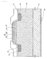
- FIG. 2 shows the schematic configuration of a general CMP apparatus.
- An SiC monocrystal substrate 14 is fixed to a polishing head 11, and is pressed to a polishing pad 13 on a turn table 12.
- a polishing slurry is dropped from a slurry supply nozzle 15, either of or both of the polishing pad 13 and the SiC monocrystal substrate 14 is rotated by a rotation motor, and the SiC monocrystal substrate 14 is polished by the chemical or mechanical action.
- a polishing slurry is composed of a solvent, abrasive grains, and an addition agent in general. For instance, fine silica grains such as colloidal silica are dispersed in water as abrasive grains, and a necessary addition agent is added to fine silica grains in water for adjusting pH.
- the epitaxial growth of SiC from the treated surface is carried out by the CVD method.
- Propane is used as the source gas of carbon
- silane is used as the source gas of silicon.
- hydrogen is used as a carrier gas
- nitrogen or trimethyl aluminum is used as a dopant gas.
- the epitaxial growth of SiC is carried out at a growth speed of the range of 2 to 20 ⁇ m per hour under the condition of the range of 1500 to 1600°C and 40 to 80 Torr in the gas ambient atmosphere.
- the step flow growth of SiC is carried out with the crystal type same as that of the substrate.
- a vertical type hot wall reactor can be used as an actual apparatus for the epitaxial growth.
- a water cooling double cylinder tube made of quartz is attached to the vertical type hot wall reactor.
- a cylindrical heat insulating material, a hot wall made of graphite, and a wedge type suscepter for holding the SiC monocrystal substrate in a vertical direction are installed in the water cooling double cylinder tube.
- a high frequency heating coil is installed on the external periphery of the water cooling double cylinder tube. The high frequency heating coil is used to heat the hot wall by high frequency induction, and the SiC monocrystal substrate that is held by the wedge type suscepter is heated by radiant heat from the hot wall.
- the epitaxial growth of SiC is carried out on the surface of the SiC monocrystal substrate by supplying a reaction gas from the lower section of the water cooling double cylinder tube while heating the SiC monocrystal substrate.
- a bipolar device is fabricated by using SiC with an epitaxial film that has been obtained as described above.
- devices such as a pn diode, a bipolar junction transistor (BJT), a thyristor, a GTO thyristor, and an IGBT are given.
- a region where an electron and a hole are recombined during current flowing is formed in the above described epitaxial layer for the bipolar devices. Since the substrate to which the above described treatment has been carried out is used in the present embodiment, a basal plane dislocation density to the epitaxial layer can be greatly reduced. As a result, the generation of a stacking fault that is converted from a basal plane dislocation during current flowing can be suppressed, and a forward voltage degradation due to long-term operation can be improved.
- the basal plane dislocation can be greatly reduced.
- an imaging force acts between a dislocation that exists in crystal and a crystal surface.
- the imaging force can be calculated by considering an imaging dislocation.
- a force F of a dislocation having an imaging relation with the dislocation is represented by the following equation (see Fig. 5(a)).
- an imaging force increases as a distance d from the crystal surface to the dislocation becomes smaller.
- the value of the imaging force is negative, thus indicating that an attracting force acts between the dislocation and the crystal surface. That is to say, as shown in Fig. 5(b), as the basal plane dislocation approaches to the crystal surface, an attracting force acts to the basal plane dislocation that exists in the SiC monocrystal in such a manner that the basal plane dislocation gradually becomes perpendicular to the crystal surface.
- the basal plane dislocation is converted to a threading edge dislocation that is propagated in the direction almost perpendicular to the crystal surface (direction parallel to a C axis).
- the surface of the epitaxial film includes the stepped surface at an atomic level (atomic step) .
- a distance d between the surface of the epitaxial film and a basal plane dislocation 41 that exists in the epitaxial film is minimized, and an imaging force (attracting force) that is applied to the basal plane dislocation 41 from the surface is maximized. Consequently, the basal plane dislocation 41 is propagated inside the epitaxial monocrystal film while changing its direction to that almost perpendicular to the crystal surface (direction of the C axis), that is, while being converted to the threading edge dislocation.
- a bunching step 43 in which several atomic steps are bundled exists on an actual crystal surface.
- an imaging force (attracting force) that is applied to the basal plane dislocation 41 from the surface is lowered. Accordingly, the basal plane dislocation 41 is propagated inside the epitaxial monocrystal film without changing its direction to that almost perpendicular to the crystal surface (direction of the C axis), that is, while being almost parallel to the crystal surface.
- the state of the atomic step on the crystal surface of the SiC monocrystal substrate during the epitaxial growth changes depending on the surface treatment to the SiC monocrystal substrate.
- the bunching of the atomic steps on the surface of the substrate is suppressed by carrying out a hydrogen etching treatment that is suitable for the surface of the substrate or carrying out both the hydrogen etching treatment and chemical mechanical polishing treatment that are suitable for the surface of the substrate.
- the existence of the bunching of the atomic steps on the surface of the substrate and the area size of a bunching step can be measured as a surface roughness Rms macroscopically.
- the surface roughness Rms can be reduced by carrying out the surface treatments before forming the epitaxial film.
- a new basal plane dislocation may be generated during the epitaxial growth in which a basal plane dislocation is propagated from the substrate to the epitaxial film.
- the density of the basal plane dislocation in the epitaxial film is a sum of basal plane dislocations that are propagated from the substrate to the epitaxial film and new basal plane dislocations that are generated during the epitaxial growth.
- a crystal imperfection on the surface of the substrate can be removed by carrying out the chemical mechanical polishing treatment or the hydrogen etching treatment under the suitable conditions and by flattening the surface of the substrate. That is to say, the density of basal plane dislocations that are generated during the epitaxial growth can be reduced by carrying out the chemical mechanical polishing treatment or the hydrogen etching treatment and by reducing the surface roughness of the substrate.
- the basal plane dislocation 41 is closer to the crystal surface. Accordingly, as the off-angle ⁇ becomes smaller, an imaging force per unit length that is applied to the basal plane dislocation 41 becomes larger. That is to say, as the off-angle ⁇ is smaller, the rate of the basal plane dislocation that is converted to the threading edge dislocation during the epitaxial growth becomes higher.
- the off-angle ⁇ becomes extremely small, the epitaxial growth on the (0001) Si plane or (000-1) C plane of the SiC monocrystal substrate is difficult. Therefore, the off-angle ⁇ of 1° or larger is necessary practically.
- a substrate that has been cut while being inclined at an off-angle of the range of 1 to 12° preferably the range of 1 to 8°, particularly preferably the range of 1 to 4°, is used, a superior quality epitaxial film to which the propagation of the basal plane dislocation from the substrate is less can be obtained.
- the (000-1) C plane has a property in which step bunching is hard to occur. Consequently, for the (000-1) C plane, an epitaxial layer in which the basal plane dislocation density is extremely small can be obtained even in the case in which the off-angle is in the range of 1 to 8°.
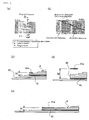
- Fig. 3 is a cross-sectional view for showing an example of a pn (pin) diode, which is one of bipolar devices.
- An ingot that has been grown by the modified Lely method is sliced at the specified off-angle.
- An n-type 4H-SiC substrate of which the surface has been polished in the specular morphology is treated by hydrogen etching or chemical mechanical polishing under the above conditions to form an SiC monocrystal substrate 21 (with a carrier density of 8 ⁇ 10 18 cm -3 and a thickness of 400 ⁇ m).
- the epitaxial growth of a nitrogen doped n-type SiC layer and that of an aluminum doped p-type SiC layer are then carried out in order on the SiC monocrystal substrate 21 by the CVD method.
- a drift layer 23 which is an n-type growth layer has a donor density of 5 ⁇ 10 14 cm -3 and a film thickness of 40 ⁇ m.
- a p-type growth layer is composed of a p-type junction layer 24 and a p + -type contact layer 25.
- the p-type junction layer 24 has an acceptor density of 5 ⁇ 10 17 cm -3 and a film thickness of 1.5 ⁇ m.
- the p + -type contact layer 25 has an acceptor density of 1 ⁇ 10 18 cm -3 and a film thickness of 0.5 ⁇ m.
- junction termination extension (JTE) 26 has a total dose of 1.2 ⁇ 10 13 cm -2 , a width of 250 ⁇ m, and a depth of 0.7 ⁇ m.
- JTE junction termination extension
- a heat treatment of 1700°C in the argon gas ambient atmosphere is carried out to activate the implanted ions.
- Numeral 27 represents a thermal oxide film that has been formed after the implanted ions were activated.
- Numeral 28 represents a cathode electrode which has been formed by evaporating Ni (with a thickness of 350 nm) under the bottom surface of the SiC monocrystal substrate 21, and numeral 29 represents an anode electrode which has been formed by evaporating a Ti film 29a (with a thickness of 350 nm) and an Al film 29b (with a thickness of 100 nm) on the p + -type contact layer 25.
- These electrodes function as an ohmic electrode by a heat treatment of 1000°C for 20 minutes after the evaporation.
- the drift layer 23 is made of an epitaxial film that has been grown from the surface of the SiC monocrystal substrate 21 which has been treated by hydrogen etching and chemical mechanical polishing, thus reducing a basal plane dislocation density in the drift layer 23. Accordingly, a conversion to a stacking fault due to recombination energy of an electron and a hole during current flowing can be suppressed, thus lengthening the life of the device.
- An ingot that was grown by an modified Lely method was sliced at an off-angle of 8° to the off-orientation of the [11-20] direction.
- the surface of the sliced substrate was smoothed in the specular morphology by mechanically polishing the surface with abrasive grains.
- an etching treatment for 40 minutes was carried out at a temperature of 1400°C and a pressure of 30 Torr to the formed n-type 4H-SiC (0001) substrate while supplying a hydrogen gas at a flow rate of 10 L/min.
- the surface roughness Rms of the substrate which was measured by using the interatomic force microscope SPI3800N manufactured by Seiko Instruments Inc. after the treatment, was 0.25 nm (region of 10 ⁇ m ⁇ 10 ⁇ m).
- An epitaxial film with a film thickness of 60 ⁇ m was formed by the step flow growth for 4 hours at a temperature of 1545°C and a pressure of 42 Torr while supplying propane (8 cc/min), silane (30 cc/min), and hydrogen (10 L/min).
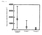
- the basal plane dislocation density in the epitaxial film which was measured by using the molten KOH etching and X-ray topograph for the SiC monocrystal substrate with the epitaxial film that was obtained, was 440 cm -2 on the average.
- the SiC monocrystal substrate with the epitaxial film was obtained similarly to the Example 1 except that the surface of the substrate was treated by chemical mechanical polishing before carrying out a hydrogen etching treatment.
- the surface roughness Rms of the substrate which was measured based on the method same as that of the Example 1 after the treatment, was 0.20 nm (region of 10 ⁇ m ⁇ 10 ⁇ m).
- the basal plane dislocation density in the epitaxial film which was measured by using the molten KOH etching and X-ray topograph for the SiC monocrystal substrate with the epitaxial film that was obtained, was 60 cm -2 on the average.
- An ingot that was grown by an modified Lely method was sliced at an off-angle of 8° to the off-orientation of the [11-20] direction.
- the surface of the sliced substrate was smoothed in the specular morphology by mechanically polishing the surface with abrasive grains.
- the formed n-type 4H-SiC (000-1) substrate was treated by chemical mechanical polishing and hydrogen etching and then an epitaxial film was grown similarly to the Example 2.
- the surface roughness Rms of the substrate which was measured based on the method same as that of the embodiment 1 after the treatment, was 0.20 nm (region of 10 ⁇ m ⁇ 10 ⁇ m).
- the basal plane dislocation density in the epitaxial film which was measured by using the molten KOH etching and X-ray topograph for the SiC monocrystal substrate with the epitaxial film that was obtained, was 20 cm -2 on the average.
- An ingot that was grown by an modified Lely method was sliced at an off-angle of 4° to the off-orientation of the [11-20] direction.
- the surface of the sliced substrate was smoothed in the specular morphology by mechanically polishing the surface with abrasive grains.
- the formed n-type 4H-SiC (0001) substrate was treated by chemical mechanical polishing and hydrogen etching and then an epitaxial film was grown similarly to the Example 2.
- the surface roughness Rms of the substrate which was measured based on the method same as that of the Example 1 after the treatment, was 0.28 nm (region of 10 ⁇ m ⁇ 10 ⁇ m).
- the basal plane dislocation density in the epitaxial film which was measured by using the molten KOH etching and X-ray topograph for the SiC monocrystal substrate with the epitaxial film that was obtained, was 20 cm -2 on the average.
- the SiC monocrystal substrate with the epitaxial film was obtained similarly to the Example 1 except that the hydrogen etching treatment was not carried out.
- Fig. 4 shows the results of the above described Examples 1 and 2 and Comparison example 1.
- n-type 4H-SiC (0001) substrate that was obtained by slicing an SiC ingot was treated by chemical mechanical polishing and hydrogen etching in this order.
- the epitaxial growth of SiC was then carried out by the CVD method to provide an SiC monocrystal substrate with an epitaxial film.
- a pn diode as shown in Fig. 3 was fabricated to obtain the pn diode related to the Example 5.
Landscapes
- Engineering & Computer Science (AREA)
- Microelectronics & Electronic Packaging (AREA)
- Power Engineering (AREA)
- Computer Hardware Design (AREA)
- Physics & Mathematics (AREA)
- Condensed Matter Physics & Semiconductors (AREA)
- General Physics & Mathematics (AREA)
- Manufacturing & Machinery (AREA)
- Chemical & Material Sciences (AREA)
- Ceramic Engineering (AREA)
- Crystallography & Structural Chemistry (AREA)
- Materials Engineering (AREA)
- Chemical Kinetics & Catalysis (AREA)
- General Chemical & Material Sciences (AREA)
- Crystals, And After-Treatments Of Crystals (AREA)
- Bipolar Transistors (AREA)
Applications Claiming Priority (2)
| Application Number | Priority Date | Filing Date | Title |
|---|---|---|---|
| JP2004092666 | 2004-03-26 | ||
| PCT/JP2005/005585 WO2005093796A1 (ja) | 2004-03-26 | 2005-03-25 | バイポーラ型半導体装置およびその製造方法 |
Publications (2)
| Publication Number | Publication Date |
|---|---|
| EP1739726A1 true EP1739726A1 (de) | 2007-01-03 |
| EP1739726A4 EP1739726A4 (de) | 2009-08-26 |
Family
ID=35056457
Family Applications (1)
| Application Number | Title | Priority Date | Filing Date |
|---|---|---|---|
| EP05721512A Withdrawn EP1739726A4 (de) | 2004-03-26 | 2005-03-25 | Bipolares halbleiterbauelement und prozess zu seiner herstellung |
Country Status (6)
| Country | Link |
|---|---|
| US (1) | US20070290211A1 (de) |
| EP (1) | EP1739726A4 (de) |
| KR (1) | KR100853991B1 (de) |
| CN (1) | CN1938820A (de) |
| TW (1) | TW200539318A (de) |
| WO (1) | WO2005093796A1 (de) |
Cited By (10)
| Publication number | Priority date | Publication date | Assignee | Title |
|---|---|---|---|---|
| EP2056340A1 (de) * | 2006-08-25 | 2009-05-06 | Sumitomo Electric Industries, Ltd. | Verfahren zur herstellung eines siliciumcarbidsubstrats und siliciumcarbidsubstrat |
| US8860040B2 (en) | 2012-09-11 | 2014-10-14 | Dow Corning Corporation | High voltage power semiconductor devices on SiC |
| US8940614B2 (en) | 2013-03-15 | 2015-01-27 | Dow Corning Corporation | SiC substrate with SiC epitaxial film |
| US9017804B2 (en) | 2013-02-05 | 2015-04-28 | Dow Corning Corporation | Method to reduce dislocations in SiC crystal growth |
| US9018639B2 (en) | 2012-10-26 | 2015-04-28 | Dow Corning Corporation | Flat SiC semiconductor substrate |
| US9349757B2 (en) | 2009-12-11 | 2016-05-24 | Semiconductor Energy Laboratory Co., Ltd. | Semiconductor device and electronic device |
| EP2472568A4 (de) * | 2009-08-28 | 2017-08-02 | Showa Denko K.K. | Epitaktischer siliciumcarbid-wafer und herstellungsverfahren dafür |
| US9738991B2 (en) | 2013-02-05 | 2017-08-22 | Dow Corning Corporation | Method for growing a SiC crystal by vapor deposition onto a seed crystal provided on a supporting shelf which permits thermal expansion |
| US9797064B2 (en) | 2013-02-05 | 2017-10-24 | Dow Corning Corporation | Method for growing a SiC crystal by vapor deposition onto a seed crystal provided on a support shelf which permits thermal expansion |
| US10002760B2 (en) | 2014-07-29 | 2018-06-19 | Dow Silicones Corporation | Method for manufacturing SiC wafer fit for integration with power device manufacturing technology |
Families Citing this family (40)
| Publication number | Priority date | Publication date | Assignee | Title |
|---|---|---|---|---|
| JP4842094B2 (ja) * | 2006-11-02 | 2011-12-21 | 新日本製鐵株式会社 | エピタキシャル炭化珪素単結晶基板の製造方法 |
| JP5147244B2 (ja) * | 2007-01-17 | 2013-02-20 | 関西電力株式会社 | バイポーラ型半導体素子 |
| JP5644105B2 (ja) * | 2007-03-26 | 2014-12-24 | 住友電気工業株式会社 | ショットキーバリアダイオードの製造方法 |
| WO2009035095A1 (ja) | 2007-09-12 | 2009-03-19 | Showa Denko K.K. | エピタキシャルSiC単結晶基板及びエピタキシャルSiC単結晶基板の製造方法 |
| WO2009048997A1 (en) * | 2007-10-12 | 2009-04-16 | The Government Of The United States Of America, As Represented By The Secretary Of The Navy | Producing epitaxial layers with low basal plane dislocation concentrations |
| JP5504597B2 (ja) * | 2007-12-11 | 2014-05-28 | 住友電気工業株式会社 | 炭化ケイ素半導体装置およびその製造方法 |
| WO2009084242A1 (ja) * | 2007-12-28 | 2009-07-09 | Sumitomo Chemical Company, Limited | 半導体基板および半導体基板の製造方法 |
| JP5243815B2 (ja) * | 2008-02-27 | 2013-07-24 | 新日本無線株式会社 | 半導体装置 |
| US8536582B2 (en) * | 2008-12-01 | 2013-09-17 | Cree, Inc. | Stable power devices on low-angle off-cut silicon carbide crystals |
| US8497552B2 (en) | 2008-12-01 | 2013-07-30 | Cree, Inc. | Semiconductor devices with current shifting regions and related methods |
| JP5436231B2 (ja) * | 2009-01-16 | 2014-03-05 | 昭和電工株式会社 | 半導体素子の製造方法及び半導体素子、並びに半導体装置 |
| US20110278596A1 (en) * | 2009-01-30 | 2011-11-17 | Takashi Aigo | Epitaxial silicon carbide monocrystalline substrate and method of production of same |
| JP5516424B2 (ja) * | 2009-02-04 | 2014-06-11 | 日立金属株式会社 | エピタキシャル成長用炭化珪素単結晶基板の製造方法 |
| JP2010184833A (ja) * | 2009-02-12 | 2010-08-26 | Denso Corp | 炭化珪素単結晶基板および炭化珪素単結晶エピタキシャルウェハ |
| KR20110133541A (ko) * | 2009-03-27 | 2011-12-13 | 스미토모덴키고교가부시키가이샤 | Mosfet 및 mosfet의 제조 방법 |
| US8030151B2 (en) * | 2009-03-27 | 2011-10-04 | National Semiconductor Corporation | Configuration and fabrication of semiconductor structure having bipolar junction transistor in which non-monocrystalline semiconductor spacing portion controls base-link length |
| US9464366B2 (en) | 2009-08-20 | 2016-10-11 | The United States Of America, As Represented By The Secretary Of The Navy | Reduction of basal plane dislocations in epitaxial SiC |
| US10256090B2 (en) | 2009-08-20 | 2019-04-09 | The United States Of America, As Represented By The Secretary Of The Navy | Reduction of basal plane dislocations in epitaxial SiC using an in-situ etch process |
| US10256094B2 (en) | 2009-08-20 | 2019-04-09 | The Government Of The United States Of America, As Represented By The Secretary Of The Navy | Reduction of basal plane dislocations in epitaxial SiC using an in-situ etch process |
| CN101877309B (zh) * | 2009-10-30 | 2011-09-21 | 西安电子科技大学 | 提高4H-SiC基面位错转化率的外延方法 |
| DE202010018325U1 (de) | 2010-03-23 | 2015-08-18 | Sumitomo Electric Industries, Inc. | Halbleitervorrichtung |
| JP5598542B2 (ja) | 2010-05-10 | 2014-10-01 | 三菱電機株式会社 | 炭化珪素エピタキシャルウエハ及びその製造方法並びにエピタキシャル成長用炭化珪素バルク基板及びその製造方法 |
| US8445386B2 (en) * | 2010-05-27 | 2013-05-21 | Cree, Inc. | Smoothing method for semiconductor material and wafers produced by same |
| JP6025306B2 (ja) * | 2011-05-16 | 2016-11-16 | 株式会社豊田中央研究所 | SiC単結晶、SiCウェハ及び半導体デバイス |
| JP5961357B2 (ja) | 2011-09-09 | 2016-08-02 | 昭和電工株式会社 | SiCエピタキシャルウェハ及びその製造方法 |
| US9994951B2 (en) | 2013-03-15 | 2018-06-12 | The United States Of America, As Represented By The Secretary Of The Navy | Photovoltaic sputtering targets fabricated from reclaimed materials |
| JP2014189442A (ja) * | 2013-03-27 | 2014-10-06 | Sumitomo Electric Ind Ltd | 炭化珪素半導体基板の製造方法 |
| JP6311384B2 (ja) | 2014-03-24 | 2018-04-18 | 三菱電機株式会社 | 炭化珪素半導体装置の製造方法 |
| CN106233430B (zh) | 2014-04-18 | 2019-08-06 | 国立研究开发法人产业技术综合研究所 | 碳化硅外延晶片及其制造方法 |
| JP6315579B2 (ja) | 2014-07-28 | 2018-04-25 | 昭和電工株式会社 | SiCエピタキシャルウェハの製造方法 |
| DE112015002906B4 (de) | 2015-02-02 | 2022-12-22 | Fuji Electric Co., Ltd. | Verfahren zur Herstellung einer Siliciumcarbid-Halbleitervorrichtung und Siliciumcarbid-Halbleitervorrichtung |
| CN104867818B (zh) * | 2015-04-02 | 2017-08-25 | 中国电子科技集团公司第十三研究所 | 一种减少碳化硅外延材料缺陷的方法 |
| CN105185820B (zh) * | 2015-08-18 | 2017-12-12 | 华中科技大学 | 一种基于碳化硅的半导体断路开关及其制备方法 |
| CN108138360B (zh) * | 2015-10-07 | 2020-12-08 | 住友电气工业株式会社 | 碳化硅外延基板及用于制造碳化硅半导体装置的方法 |
| WO2018016171A1 (ja) * | 2016-07-21 | 2018-01-25 | 三菱電機株式会社 | 炭化珪素半導体装置、および、炭化珪素半導体装置の製造方法 |
| CN107910360A (zh) * | 2017-12-06 | 2018-04-13 | 中国工程物理研究院电子工程研究所 | 一种新型碳化硅小角度倾斜台面终端结构及其制备方法 |
| JP6481790B2 (ja) * | 2018-03-20 | 2019-03-13 | 昭和電工株式会社 | SiCエピタキシャルウェハ |
| US20220059658A1 (en) * | 2018-12-04 | 2022-02-24 | Sumitomo Electric Industries, Ltd. | Silicon carbide epitaxial substrate and silicon carbide semiconductor device |
| CN115223846A (zh) * | 2021-04-15 | 2022-10-21 | 环球晶圆股份有限公司 | 半导体衬底的制造方法 |
| CN115635380B (zh) * | 2022-12-26 | 2023-03-17 | 华芯半导体研究院(北京)有限公司 | 一种气相外延生长辅助装置 |
Citations (1)
| Publication number | Priority date | Publication date | Assignee | Title |
|---|---|---|---|---|
| EP1306890A2 (de) * | 2001-10-25 | 2003-05-02 | Matsushita Electric Industrial Co., Ltd. | Halbleitersubstrat und -bauelement aus SiC und Verfahren zu deren Herstellung |
Family Cites Families (7)
| Publication number | Priority date | Publication date | Assignee | Title |
|---|---|---|---|---|
| US4684413A (en) * | 1985-10-07 | 1987-08-04 | Rca Corporation | Method for increasing the switching speed of a semiconductor device by neutron irradiation |
| JPH10261615A (ja) * | 1997-03-17 | 1998-09-29 | Fuji Electric Co Ltd | SiC半導体の表面モホロジー制御方法およびSiC半導体薄膜の成長方法 |
| JP2001077030A (ja) * | 1999-08-31 | 2001-03-23 | Sanyo Electric Co Ltd | 炭化珪素半導体装置の製造方法 |
| JP4581270B2 (ja) * | 2001-03-05 | 2010-11-17 | 住友電気工業株式会社 | SiC半導体のイオン注入層及びその製造方法 |
| US6849874B2 (en) * | 2001-10-26 | 2005-02-01 | Cree, Inc. | Minimizing degradation of SiC bipolar semiconductor devices |
| JP3929375B2 (ja) * | 2002-08-06 | 2007-06-13 | 三菱電機株式会社 | 半導体結晶基板の評価方法 |
| TWI272874B (en) * | 2002-08-09 | 2007-02-01 | Semiconductor Energy Lab | Organic electroluminescent device |
-
2005
- 2005-03-25 US US10/594,045 patent/US20070290211A1/en not_active Abandoned
- 2005-03-25 WO PCT/JP2005/005585 patent/WO2005093796A1/ja active Application Filing
- 2005-03-25 KR KR1020067022103A patent/KR100853991B1/ko not_active IP Right Cessation
- 2005-03-25 EP EP05721512A patent/EP1739726A4/de not_active Withdrawn
- 2005-03-25 CN CNA200580009661XA patent/CN1938820A/zh active Pending
- 2005-03-28 TW TW094109526A patent/TW200539318A/zh unknown
Patent Citations (1)
| Publication number | Priority date | Publication date | Assignee | Title |
|---|---|---|---|---|
| EP1306890A2 (de) * | 2001-10-25 | 2003-05-02 | Matsushita Electric Industrial Co., Ltd. | Halbleitersubstrat und -bauelement aus SiC und Verfahren zu deren Herstellung |
Non-Patent Citations (5)
| Title |
|---|
| DOGAN S ET AL: "The effect of hydrogen etching on 6H-SiC studied by temperature-dependent current-voltage and atomic force microscopy" APPLIED PHYSICS LETTERS, AIP, AMERICAN INSTITUTE OF PHYSICS, MELVILLE, NY, US, vol. 85, no. 9, 30 August 2004 (2004-08-30), pages 1547-1549, XP012064354 ISSN: 0003-6951 * |
| HALLIN C ET AL: "In situ substrate preparation for high-quality SiC chemical vapour deposition" JOURNAL OF CRYSTAL GROWTH, ELSEVIER, AMSTERDAM, NL, vol. 181, no. 3, 1 November 1997 (1997-11-01), pages 241-253, XP004095406 ISSN: 0022-0248 * |
| LANDINI B E ET AL: "4H-SIC SUBSTRATE ORIENTATION EFFECTS ON HYDROGEN ETCHING AND EPITAXIAL GROWTH" MATERIALS SCIENCE FORUM, AEDERMANNSFDORF, CH, vol. 338-342, 1 January 2000 (2000-01-01), pages 185-188, XP009083296 ISSN: 0255-5476 * |
| LENDENMANN H ET AL: "High-power SiC diodes: characteristics, reliability and relation to material defects" MATERIALS SCIENCE FORUM, AEDERMANNSFDORF, CH, vol. 389-393, 1 January 2002 (2002-01-01), pages 1259-1264, XP009120191 ISSN: 0255-5476 * |
| See also references of WO2005093796A1 * |
Cited By (19)
| Publication number | Priority date | Publication date | Assignee | Title |
|---|---|---|---|---|
| EP2056340A4 (de) * | 2006-08-25 | 2011-01-12 | Sumitomo Electric Industries | Verfahren zur herstellung eines siliciumcarbidsubstrats und siliciumcarbidsubstrat |
| CN101536157B (zh) * | 2006-08-25 | 2012-05-30 | 住友电气工业株式会社 | 用于制造碳化硅衬底的方法以及碳化硅衬底 |
| EP2056340A1 (de) * | 2006-08-25 | 2009-05-06 | Sumitomo Electric Industries, Ltd. | Verfahren zur herstellung eines siliciumcarbidsubstrats und siliciumcarbidsubstrat |
| EP2472568A4 (de) * | 2009-08-28 | 2017-08-02 | Showa Denko K.K. | Epitaktischer siliciumcarbid-wafer und herstellungsverfahren dafür |
| US10600818B2 (en) | 2009-12-11 | 2020-03-24 | Semiconductor Energy Laboratory Co., Ltd. | Semiconductor device and electronic device |
| US10312267B2 (en) | 2009-12-11 | 2019-06-04 | Semiconductor Energy Laboratory Co., Ltd. | Semiconductor device and electronic device |
| US11961843B2 (en) | 2009-12-11 | 2024-04-16 | Semiconductor Energy Laboratory Co., Ltd. | Semiconductor device and electronic device |
| US10854641B2 (en) | 2009-12-11 | 2020-12-01 | Semiconductor Energy Laboratory Co., Ltd. | Semiconductor device and electronic device |
| US10002888B2 (en) | 2009-12-11 | 2018-06-19 | Semiconductor Energy Laboratory Co., Ltd. | Semiconductor device and electronic device |
| US9349757B2 (en) | 2009-12-11 | 2016-05-24 | Semiconductor Energy Laboratory Co., Ltd. | Semiconductor device and electronic device |
| US9735180B2 (en) | 2009-12-11 | 2017-08-15 | Semiconductor Energy Laboratory Co., Ltd. | Semiconductor device and electronic device |
| US8860040B2 (en) | 2012-09-11 | 2014-10-14 | Dow Corning Corporation | High voltage power semiconductor devices on SiC |
| US9165779B2 (en) | 2012-10-26 | 2015-10-20 | Dow Corning Corporation | Flat SiC semiconductor substrate |
| US9018639B2 (en) | 2012-10-26 | 2015-04-28 | Dow Corning Corporation | Flat SiC semiconductor substrate |
| US9797064B2 (en) | 2013-02-05 | 2017-10-24 | Dow Corning Corporation | Method for growing a SiC crystal by vapor deposition onto a seed crystal provided on a support shelf which permits thermal expansion |
| US9738991B2 (en) | 2013-02-05 | 2017-08-22 | Dow Corning Corporation | Method for growing a SiC crystal by vapor deposition onto a seed crystal provided on a supporting shelf which permits thermal expansion |
| US9017804B2 (en) | 2013-02-05 | 2015-04-28 | Dow Corning Corporation | Method to reduce dislocations in SiC crystal growth |
| US8940614B2 (en) | 2013-03-15 | 2015-01-27 | Dow Corning Corporation | SiC substrate with SiC epitaxial film |
| US10002760B2 (en) | 2014-07-29 | 2018-06-19 | Dow Silicones Corporation | Method for manufacturing SiC wafer fit for integration with power device manufacturing technology |
Also Published As
| Publication number | Publication date |
|---|---|
| EP1739726A4 (de) | 2009-08-26 |
| TW200539318A (en) | 2005-12-01 |
| KR20070029694A (ko) | 2007-03-14 |
| KR100853991B1 (ko) | 2008-08-25 |
| WO2005093796A1 (ja) | 2005-10-06 |
| CN1938820A (zh) | 2007-03-28 |
| US20070290211A1 (en) | 2007-12-20 |
Similar Documents
| Publication | Publication Date | Title |
|---|---|---|
| EP1739726A1 (de) | Bipolares halbleiterbauelement und prozess zu seiner herstellung | |
| JP5285202B2 (ja) | バイポーラ型半導体装置およびその製造方法 | |
| EP1215730B9 (de) | SiC-HALBLEITERSCHEIBE, SiC-HALBLEITERBAUELEMENT SOWIE HERSTELLUNGSVERFAHREN FÜR EINE SiC-HALBLEITERSCHEIBE | |
| JP4185215B2 (ja) | SiCウエハ、SiC半導体デバイス、および、SiCウエハの製造方法 | |
| EP1933386B1 (de) | Prozess zum herstellen einer siliziumcarbid-halbleiteranordnung | |
| EP1981076B1 (de) | Verfahren zur herstellung einer siliziumcarbid-halbleiteranordnung | |
| US7507650B2 (en) | Process for producing Schottky junction type semiconductor device | |
| US6660084B1 (en) | Sic single crystal and method for growing the same | |
| EP1306890A2 (de) | Halbleitersubstrat und -bauelement aus SiC und Verfahren zu deren Herstellung | |
| JP4021448B2 (ja) | ショットキー接合型半導体装置の製造方法 | |
| JP4879507B2 (ja) | バイポーラ型半導体装置の順方向電圧回復方法、積層欠陥縮小方法およびバイポーラ型半導体装置 | |
| KR20120023710A (ko) | 반도체 장치 | |
| US20170179236A1 (en) | Method of producing silicon carbide epitaxial substrate, silicon carbide epitaxial substrate, and silicon carbide semiconductor device | |
| JP2007131504A (ja) | SiCエピタキシャルウエーハおよびそれを用いた半導体デバイス | |
| US20220336589A1 (en) | Contact structures for n-type diamond | |
| US8455269B2 (en) | Method for recovering an on-state forward voltage and, shrinking stacking faults in bipolar semiconductor devices, and the bipolar semiconductor devices | |
| US20130341648A1 (en) | Method for manufacturing silicon carbide semiconductor device and silicon carbide semiconductor device | |
| JP2007027630A (ja) | バイポーラ型半導体装置およびその製造方法 | |
| JP2007235162A (ja) | ショットキー接合型半導体装置 | |
| JP2006237125A (ja) | バイポーラ型半導体装置の運転方法およびバイポーラ型半導体装置 | |
| WO2008015764A1 (fr) | Procédé de fonctionnement d'un dispositif semi-conducteur bipolaire et dispositif semi-conducteur bipolaire | |
| WO2008015765A1 (fr) | Dispositif a semi-conducteurs bipolaire et son procédé de production |
Legal Events
| Date | Code | Title | Description |
|---|---|---|---|
| PUAI | Public reference made under article 153(3) epc to a published international application that has entered the european phase |
Free format text: ORIGINAL CODE: 0009012 |
|
| 17P | Request for examination filed |
Effective date: 20061026 |
|
| AK | Designated contracting states |
Kind code of ref document: A1 Designated state(s): DE FR IT SE |
|
| DAX | Request for extension of the european patent (deleted) | ||
| RBV | Designated contracting states (corrected) |
Designated state(s): DE FR IT SE |
|
| A4 | Supplementary search report drawn up and despatched |
Effective date: 20090727 |
|
| STAA | Information on the status of an ep patent application or granted ep patent |
Free format text: STATUS: THE APPLICATION IS DEEMED TO BE WITHDRAWN |
|
| 18D | Application deemed to be withdrawn |
Effective date: 20091024 |