EP1730249B1 - Dispositif electroluminescent avec hote derive anthracene - Google Patents
Dispositif electroluminescent avec hote derive anthracene Download PDFInfo
- Publication number
- EP1730249B1 EP1730249B1 EP05725437A EP05725437A EP1730249B1 EP 1730249 B1 EP1730249 B1 EP 1730249B1 EP 05725437 A EP05725437 A EP 05725437A EP 05725437 A EP05725437 A EP 05725437A EP 1730249 B1 EP1730249 B1 EP 1730249B1
- Authority
- EP
- European Patent Office
- Prior art keywords
- anthracene
- group
- materials
- inv
- light
- Prior art date
- Legal status (The legal status is an assumption and is not a legal conclusion. Google has not performed a legal analysis and makes no representation as to the accuracy of the status listed.)
- Active
Links
- 0 Bc1c(*(*)c(c(*)c(c(N(BI=I)c(c(*)c2*)c3c(*)c2I)c2C4*=C4)C3=O)c2C2=O)c2c(C)c(*)c1* Chemical compound Bc1c(*(*)c(c(*)c(c(N(BI=I)c(c(*)c2*)c3c(*)c2I)c2C4*=C4)C3=O)c2C2=O)c2c(C)c(*)c1* 0.000 description 7
- MSDMPJCOOXURQD-UHFFFAOYSA-N CC(C)(CCN1c2c3C(C)(C)CC1)c2cc(C=C1c2nc4ccccc4[s]2)c3OC1=O Chemical compound CC(C)(CCN1c2c3C(C)(C)CC1)c2cc(C=C1c2nc4ccccc4[s]2)c3OC1=O MSDMPJCOOXURQD-UHFFFAOYSA-N 0.000 description 1
- GWBBMJSNUPGHPT-UHFFFAOYSA-N CC(c(cc1)ccc1-c(cc1)cc2c1c(-c1cc3ccccc3cc1)c(cccc1)c1c2-c1cc2ccccc2cc1)(NC)O Chemical compound CC(c(cc1)ccc1-c(cc1)cc2c1c(-c1cc3ccccc3cc1)c(cccc1)c1c2-c1cc2ccccc2cc1)(NC)O GWBBMJSNUPGHPT-UHFFFAOYSA-N 0.000 description 1
- QQHNCYDVBDECQK-NWRNMNSGSA-N CNc1c(/C=C\C(/N=C2\N(C)c3ccccc3C=C2)=O)cccc1 Chemical compound CNc1c(/C=C\C(/N=C2\N(C)c3ccccc3C=C2)=O)cccc1 QQHNCYDVBDECQK-NWRNMNSGSA-N 0.000 description 1
Images

Classifications
-
- H—ELECTRICITY
- H05—ELECTRIC TECHNIQUES NOT OTHERWISE PROVIDED FOR
- H05B—ELECTRIC HEATING; ELECTRIC LIGHT SOURCES NOT OTHERWISE PROVIDED FOR; CIRCUIT ARRANGEMENTS FOR ELECTRIC LIGHT SOURCES, IN GENERAL
- H05B33/00—Electroluminescent light sources
- H05B33/12—Light sources with substantially two-dimensional radiating surfaces
- H05B33/14—Light sources with substantially two-dimensional radiating surfaces characterised by the chemical or physical composition or the arrangement of the electroluminescent material, or by the simultaneous addition of the electroluminescent material in or onto the light source
-
- C—CHEMISTRY; METALLURGY
- C09—DYES; PAINTS; POLISHES; NATURAL RESINS; ADHESIVES; COMPOSITIONS NOT OTHERWISE PROVIDED FOR; APPLICATIONS OF MATERIALS NOT OTHERWISE PROVIDED FOR
- C09K—MATERIALS FOR MISCELLANEOUS APPLICATIONS, NOT PROVIDED FOR ELSEWHERE
- C09K11/00—Luminescent, e.g. electroluminescent, chemiluminescent materials
- C09K11/06—Luminescent, e.g. electroluminescent, chemiluminescent materials containing organic luminescent materials
-
- H—ELECTRICITY
- H10—SEMICONDUCTOR DEVICES; ELECTRIC SOLID-STATE DEVICES NOT OTHERWISE PROVIDED FOR
- H10K—ORGANIC ELECTRIC SOLID-STATE DEVICES
- H10K85/00—Organic materials used in the body or electrodes of devices covered by this subclass
- H10K85/60—Organic compounds having low molecular weight
- H10K85/615—Polycyclic condensed aromatic hydrocarbons, e.g. anthracene
- H10K85/626—Polycyclic condensed aromatic hydrocarbons, e.g. anthracene containing more than one polycyclic condensed aromatic rings, e.g. bis-anthracene
-
- C—CHEMISTRY; METALLURGY
- C09—DYES; PAINTS; POLISHES; NATURAL RESINS; ADHESIVES; COMPOSITIONS NOT OTHERWISE PROVIDED FOR; APPLICATIONS OF MATERIALS NOT OTHERWISE PROVIDED FOR
- C09K—MATERIALS FOR MISCELLANEOUS APPLICATIONS, NOT PROVIDED FOR ELSEWHERE
- C09K2211/00—Chemical nature of organic luminescent or tenebrescent compounds
- C09K2211/10—Non-macromolecular compounds
- C09K2211/1003—Carbocyclic compounds
- C09K2211/1011—Condensed systems
-
- H—ELECTRICITY
- H10—SEMICONDUCTOR DEVICES; ELECTRIC SOLID-STATE DEVICES NOT OTHERWISE PROVIDED FOR
- H10K—ORGANIC ELECTRIC SOLID-STATE DEVICES
- H10K50/00—Organic light-emitting devices
- H10K50/10—OLEDs or polymer light-emitting diodes [PLED]
- H10K50/11—OLEDs or polymer light-emitting diodes [PLED] characterised by the electroluminescent [EL] layers
-
- H—ELECTRICITY
- H10—SEMICONDUCTOR DEVICES; ELECTRIC SOLID-STATE DEVICES NOT OTHERWISE PROVIDED FOR
- H10K—ORGANIC ELECTRIC SOLID-STATE DEVICES
- H10K85/00—Organic materials used in the body or electrodes of devices covered by this subclass
- H10K85/30—Coordination compounds
- H10K85/321—Metal complexes comprising a group IIIA element, e.g. Tris (8-hydroxyquinoline) gallium [Gaq3]
- H10K85/324—Metal complexes comprising a group IIIA element, e.g. Tris (8-hydroxyquinoline) gallium [Gaq3] comprising aluminium, e.g. Alq3
-
- H—ELECTRICITY
- H10—SEMICONDUCTOR DEVICES; ELECTRIC SOLID-STATE DEVICES NOT OTHERWISE PROVIDED FOR
- H10K—ORGANIC ELECTRIC SOLID-STATE DEVICES
- H10K85/00—Organic materials used in the body or electrodes of devices covered by this subclass
- H10K85/60—Organic compounds having low molecular weight
- H10K85/631—Amine compounds having at least two aryl rest on at least one amine-nitrogen atom, e.g. triphenylamine
-
- H—ELECTRICITY
- H10—SEMICONDUCTOR DEVICES; ELECTRIC SOLID-STATE DEVICES NOT OTHERWISE PROVIDED FOR
- H10K—ORGANIC ELECTRIC SOLID-STATE DEVICES
- H10K85/00—Organic materials used in the body or electrodes of devices covered by this subclass
- H10K85/60—Organic compounds having low molecular weight
- H10K85/649—Aromatic compounds comprising a hetero atom
Definitions
- This invention relates to organic electroluminescent (EL) devices comprising a light-emitting layer containing a host and a light-emitting material where the host comprises a particular anthracene compound with good operational stability.
- EL organic electroluminescent
- an organic EL device is comprised of an anode for hole injection, a cathode for electron injection, and an organic medium sandwiched between these electrodes to support charge recombination that yields emission of light. These devices are also commonly referred to as organic light-emitting diodes, or OLEDs. Representative of earlier organic EL devices are Gurnee et al. US 3,172,862, issued Mar. 9, 1965 ; Gurnee US 3,173,050, issued Mar.
- organic EL devices include an organic EL element consisting of extremely thin layers (e.g., less than 1.0 ⁇ m) between the anode and the cathode.
- organic EL element encompasses the layers between the anode and cathode. Reducing the thickness lowered the resistance of the organic layer and has enabled devices that operate at much lower voltage.
- one organic layer of the EL element adjacent to the anode is specifically chosen to transport holes, and therefore, it is referred to as the hole-transporting layer, and the other organic layer is specifically chosen to transport electrons, and is referred to as the electron-transporting layer. Recombination of the injected holes and electrons within the organic EL element results in efficient electroluminescence.
- Anthracene based hosts are often used in EL devices.
- a useful class of 9,10-di-(2-naphthyl)anthracene hosts has been disclosed in US 5,935,721 .
- Bis-anthracene compounds used in the luminescent layer with an improved device half-life have been disclosed in US 6,534,199 and US 2002/0136922 .
- Electroluminescent devices with improved luminance using anthracene compound have been disclosed in US 6,582,837 .
- Anthracenes have also been used in the HTL as disclosed in US 6,465,1115 .
- the invention provides an electroluminescent device comprising a light emitting layer including an anthracene material bearing at least one aryl ring in the 2-position and having a hydrogen or an alkyl group in the 6-position and having up to 12 aromatic carbocyclic rings including at least one naphthalene group in the 9-position of the anthracene group and an aryl group in the 10-position, the anthracene material including among the rings only carbocyclic rings, provided that the anthracene does not have either one of the structures or
- the invention also includes the anthracene compound as well as a display, a lighting device, and a process employing the electroluminescent device
- Embodiments of the invention provide high luminance yield, have improved operational stability and a desirable hue and that are conveniently manufactured.
- an electroluminescent device of the invention is a multilayer device comprising a cathode, an anode, charge-injecting layers (if necessary), charge-transporting layers, and at least one light-emitting layer (LEL) comprising a host and at least one light-emitting material.
- LEL light-emitting layer
- the device includes a layer containing an anthracene material bearing at least one aryl ring in the 2-position, for example, a phenyl group, a naphthyl group or a biphenyl group.
- the anthracene material also bears a hydrogen or alkyl group, such as a methyl or t -butyl, group in the 6-position.
- the anthracene material comprises up to 12 aromatic carbocyclic rings and including among the rings only carbocyclic rings. In one desirable embodiment the anthracene comprises up to 10 aromatic carbocyclic rings.
- the anthracene material includes at least one naphthalene group in the 9-position of the anthracene.
- the naphthalene group is a 2-naphthyl group.
- the 10-position of the anthracene is aryl substituted.
- the aryl substituent is a naphthyl group, such as a 2-naphthyl group or a biphenyl group, such as a 4-biphenyl group.
- the 9- and 10-positions are substituted with the same naphthyl group.
- the anthracene material comprises only one anthracene moiety, that is, there is only one anthracene group present in the compound.
- the anthracene material comprises only two anthracene moieties, that is, there are two independently selected anthracene groups present in the comppound.
- the anthracene material is represented by Formula (1),
- Ar 2 represents an aryl group, such as a phenyl group, a naphthyl group or a biphenyl group.
- Ar 9 represents a naphthyl group, such as a 2-naphthyl group or a 1-naphthyl group.
- Ar 10 represents an aryl group. Examples of aryl groups are phenyl groups, tolyl groups, naphthyl groups and biphenyl groups.
- v 1 , v 3 , v 4 , v 5 , v 7 , and v 8 independently represent hydrogen or an independently selected substituent group, such as an aryl group, for example a phenyl group, or an alkyl groups such as a t -butyl group.
- v 6 represents hydrogen or an alkyl group, such as a t -butyl group.
- the anthracene material is in a layer that includes a light emitting material.
- the anthracene material comprises the host material, and there may be more than one host materials.
- the light-emitting material(s) is present in an amount of up to 15 vol. % of the host, commonly 0.1 - 10 vol. % and more typically from 0.1-5.0 vol. % of the host.
- the anthracene material may also be part of an oligomer or a polymer having a main chain or a side chain of repeating units.
- at least one layer of the EL device comprises polymeric material.
- at least two layers of the EL device comprise polymeric material.
- An important relationship for choosing a light-emitting fluorescent material for use with a host is a comparison of the excited singlet-state energies of the host and the fluorescent material. It is highly desirable that the excited singlet-state energy of the light-emitting material be lower than that of the host material.
- the excited singlet-state energy is defined as the difference in energy between the emitting singlet state and the ground state. For non-emissive hosts, the lowest excited state of the same electronic spin as the ground state is considered the emitting state.
- the layer may emit light ranging from blue to red depending on the nature of the light-emitting material.
- Blue light is generally defined as having a wavelength range in the visible region of the electromagnetic spectrum of 450-480 nm, blue-green 480-510 nm, green 510-550, green-yellow 550-570 nm, yellow 570-90 nm, orange 590-630 nm and red 630-700 nm, as defined by R. W. Hunt, The Reproduction of Colour in Photography, Printing & Television, 4th Edition 1987, Fountain Press . Suitable combinations of these components produce white light. When light has a spectral profile that overlaps these ranges, to whatever degree, it is loosely referred to as having both color components for example, blue-green, yellow-orange or orange-red.
- Anthracene materials of the invention may be especially useful hosts for blue or blue-green materials. Many materials that emit blue or blue-green light are known in the art and are contemplated for use in the practice of the present invention. Particularly useful classes of blue emitters include perylene and its derivatives such as a perylene nucleus bearing one or more substituents such as an alkyl group or an aryl group. A desirable perylene derivative for use as an emitting material is 2,5,8,11-tetra- t -butylperylene.
- Another useful class of fluorescent materials includes blue or blue-green light emitting derivatives of distyrylarenes, such as distyrylbenzene and distyrylbiphenyl, including compounds described in US 5,121,029 .
- derivatives of distyrylarenes that provide blue or blue-green luminescence particularly useful are those substituted with diarylamino groups, also known as distyrylamines.
- Examples include Formula 2a and 2b, listed below, wherein R a - R h can be the same or different, and individually represent hydrogen or one or more substituents.
- substituents can be alkyl groups, such as methyl groups, or aryl groups, such as phenyl groups.
- Illustrative examples of useful distyrylamines are blue or blue green emitters, (2c) and (2d) listed below.
- Another useful class of blue or blue green emitters comprise a boron atom.
- Desirable light-emitting materials that contain boron include those described in US 2003/0198829 and US 2003/0201415 .
- Suitable blue or blue-green light-emitting materials are represented by the structure Formula (3a).
- Ar a and Ar b independently represent the atoms necessary to form a five or six-membered aromatic ring group, such as a pyridine group.
- Z a and Z b represent independently selected substituents, such as fluoro substituents.
- w represents N or C-Y, wherein Y represents hydrogen or a substituent, such as an aromatic group, such as a phenyl group or a tolyl group, an alkyl group, such as a methyl group, a cyano substituent, or a trifluoromethyl substituent.
- a particularly useful class of green light-emitting material includes quinacridone compounds.
- Useful quinacridones are described US 2004/0001969 , US 6,664,396 , US 5,593,788 , and JP 09-13026 .
- the light-emitting material in the light-emitting layer is a quinacridone compound represented by Formula (4).
- s 1 -s 10 independently represent hydrogen or an independently selected substituent, such as a phenyl group, a tolyl group, a halogen such as F, or an alkyl group, such as a methyl group. Adjacent substituents may combine to form rings, such as fused benzene ring groups.
- s 11 and s 12 independently represent an alkyl group or an aromatic group.
- s 11 and s 12 independently represent a phenyl ring group, such as a phenyl ring or a tolyl ring.
- Another particularly useful class of green light-emitting materials includes coumarin compounds.
- useful coumarins are described in Tang et al., US 4,769,292 and US 6,020,078 .
- the third material in the light-emitting layer is a coumarin represented by Formula (5).
- w 11 and w 12 represent an independently selected substituent, such as an alkyl group or aryl group, provided w 11 and w 12 may combine with each other or with w 13 and w 14 to form rings. Desirably w 11 and w 12 represent independently selected alkyl groups, provided w 11 and w 12 may combine with each other or with w 13 and w 14 to form saturated rings.
- w 13 -w 16 independently represent hydrogen or an independently selected substituent, such as phenyl ring group or a methyl group. Adjacent substituents may combine to form rings, such as fused benzene rings.
- w 17 represents the atoms necessary to complete a heteroaromatic ring, such as a benzothiazole ring group. Illustrative examples of useful coumarin compounds are shown below.
- Examples of additional useful emitting materials include derivatives of anthracene, fluorene, periflanthene, and indenoperylene.
- Anthracenes employed in the invention are useful in EL devices that exhibit high efficiencies and good operating stability. These compounds are useful in EL devices that produce white light as well as in full color EL devices and motion imaging devices.
- the device of the invention has more than one layer that emits light.
- the device produces white light.
- one layer of the device contains rubrene or a derivative of rubrene.
- Useful anthracene materials may be made by various methods. For example, by the method shown in the reaction steps Rx-A through Rx-C. Reaction of a bromo-aryl compound (Ar 1 Br) with a lithium reagent, for example t- butyllithium, forms the aryl-lithium salt, which then can react with compound E-1, to form E-2 (Rx-A). Dehydration of E-2 and aromatization with, for example, KI, NaH 2 PO 2 , and acetic acid, affords the anthracene E-3 (Rx-B).
- a bromo-aryl compound Ar 1 Br
- a lithium reagent for example t- butyllithium
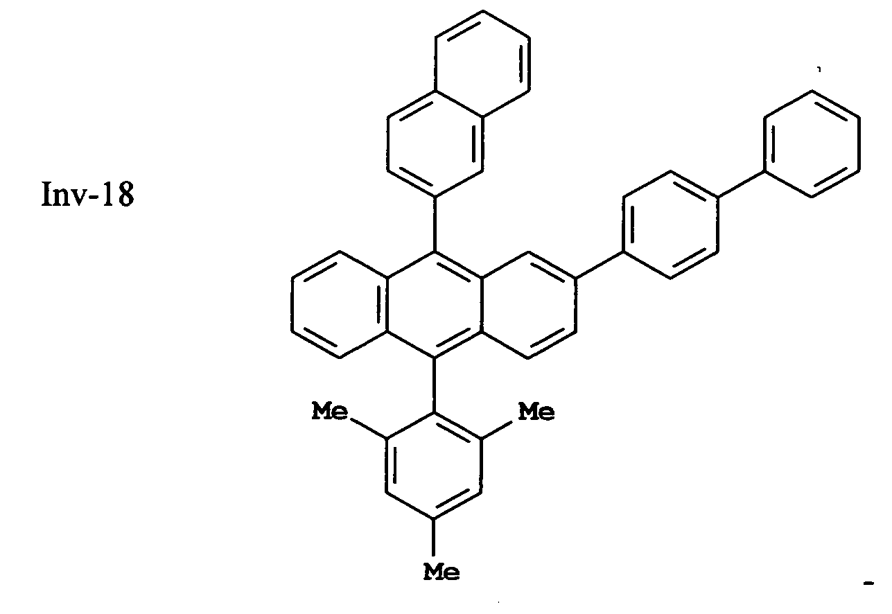
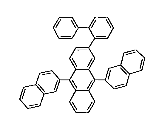
- Useful compounds of this invention include:
- substituted or “substituent” means any group or atom other than hydrogen.
- group when the term “group” is used, it means that when a substituent group contains a substitutable hydrogen, it is also intended to encompass not only the substituent's unsubstituted form, but also its form further substituted with any substituent group or groups as herein mentioned, so long as the substituent does not destroy properties necessary for device utility.
- a substituent group may be halogen or may be bonded to the remainder of the molecule by an atom of carbon, silicon, oxygen, nitrogen, phosphorous, sulfur, selenium, or boron.
- the substituent may be, for example, halogen, such as chloro, bromo or fluoro; nitro; hydroxyl; cyano; carboxyl; or groups which may be further substituted, such as alkyl, including straight or branched chain or cyclic alkyl, such as methyl, trifluoromethyl, ethyl, t -butyl, 3-(2,4-di- t -pentylphenoxy) propyl, and tetradecyl; alkenyl, such as ethylene, 2-butene; alkoxy, such as methoxy, ethoxy, propoxy, butoxy, 2-methoxyethoxy, sec-butoxy, hexyloxy, 2-ethylhexyloxy, tetradecyloxy, 2-(2,4-di- t -pentylphenoxy)ethoxy, and 2-dodecyloxyethoxy; aryl such as phenyl, 4- t
- the substituents may themselves be further substituted one or more times with the described substituent groups.
- the particular substituents used may be selected by those skilled in the art to attain the desired desirable properties for a specific application and can include, for example, electron-withdrawing groups, electron-donating groups, and steric groups.
- the substituents may be joined together to form a ring such as a fused ring unless otherwise provided.
- the above groups and substituents thereof may include those having up to 48 carbon atoms, typically 1 to 36 carbon atoms and usually less than 24 carbon atoms, but greater numbers are possible depending on the particular substituents selected.
- the present invention can be employed in many EL device configurations using small molecule materials, oligomeric materials, polymeric materials, or combinations thereof. These include very simple structures comprising a single anode and cathode to more complex devices, such as passive matrix displays comprised of orthogonal arrays of anodes and cathodes to form pixels, and active-matrix displays where each pixel is controlled independently, for example, with thin film transistors (TFTs).
- TFTs thin film transistors
- OLED organic light-emitting diode
- cathode an organic light-emitting layer located between the anode and cathode. Additional layers may be employed as more fully described hereafter.
- FIG. 1 A typical structure according to the present invention and especially useful for a small molecule device, is shown in FIG. 1 and is comprised of a substrate 101, an anode 103, a hole-injecting layer 105, a hole-transporting layer 107, a light-emitting layer 109, an electron-transporting layer 111, and a cathode 113. These layers are described in detail below. Note that the substrate 101 may alternatively be located adjacent to the cathode 113, or the substrate 101 may actually constitute the anode 103 or cathode 113.
- the organic layers between the anode 103 and cathode 113 are conveniently referred to as the organic EL element. Also, the total combined thickness of the organic layers is desirably less than 500 nm. If the device includes phosphorescent material, a hole-blocking layer, located between the light-emitting layer and the electron-transporting layer, may be present.
- the anode 103 and cathode 113 of the OLED are connected to a voltage/current source through electrical conductors.
- the OLED is operated by applying a potential between the anode 103 and cathode 113 such that the anode 103 is at a more positive potential than the cathode 113. Holes are injected into the organic EL element from the anode 103 and electrons are injected into the organic EL element at the cathode 113.
- Enhanced device stability can sometimes be achieved when the OLED is operated in an AC mode where, for some time period in the AC cycle, the potential bias is reversed and no current flows.
- An example of an AC driven OLED is described in US 5,552,678 .
- the OLED device of this invention is typically provided over a supporting substrate 101 where either the cathode 113 or anode 103 can be in contact with the substrate.
- the electrode in contact with the substrate 101 is conveniently referred to as the bottom electrode.
- the bottom electrode is the anode 103, but this invention is not limited to that configuration.
- the substrate 101 can either be light transmissive or opaque, depending on the intended direction of light emission. The light transmissive property is desirable for viewing the EL emission through the substrate 101. Transparent glass or plastic is commonly employed in such cases.
- the substrate 101 can be a complex structure comprising multiple layers of materials. This is typically the case for active matrix substrates wherein TFTs are provided below the OLED layers.
- the substrate 101 at least in the emissive pixelated areas, be comprised of largely transparent materials such as glass or polymers.
- the transmissive characteristic of the bottom support is immaterial, and therefore the substrate can be light transmissive, light absorbing or light reflective.
- Substrates for use in this case include, but are not limited to, glass, plastic, semiconductor materials such as silicon, ceramics, and circuit board materials.
- the substrate 101 can be a complex structure comprising multiple layers of materials such as found in active matrix TFT designs. It is necessary to provide in these device configurations a light-transparent top electrode.
- the anode 103 When the desired electroluminescent light emission (EL) is viewed through the anode, the anode 103 should be transparent or substantially transparent to the emission of interest.
- Common transparent anode materials used in this invention are indium-tin oxide (ITO), indium-zinc oxide (IZO) and tin oxide, but other metal oxides can work including, but not limited to, aluminum- or indium-doped zinc oxide, magnesium-indium oxide, and nickel-tungsten oxide.
- metal nitrides such as gallium nitride
- metal selenides such as zinc selenide
- metal sulfides such as zinc sulfide
- the transmissive characteristics of the anode 103 are immaterial and any conductive material can be used, transparent, opaque or reflective.
- Example conductors for this application include, but are not limited to, gold, iridium, molybdenum, palladium, and platinum.
- Typical anode materials, transmissive or otherwise, have a work function of 4.1 eV or greater. Desired anode materials are commonly deposited by any suitable means such as evaporation, sputtering, chemical vapor deposition, or electrochemical means.
- Anodes can be patterned using well-known photolithographic processes. Optionally, anodes may be polished prior to application of other layers to reduce surface roughness so as to minimize short circuits or enhance reflectivity.
- the cathode 113 used in this invention can be comprised of nearly any conductive material. Desirable materials have good film-forming properties to ensure good contact with the underlying organic layer, promote electron injection at low voltage, and have good stability. Useful cathode materials often contain a low work function metal ( ⁇ 4.0 eV) or metal alloy.
- One useful cathode material is comprised of a Mg:Ag alloy wherein the percentage of silver is in the range of 1 to 20 %, as described in U.S. Patent No. 4,885,221 .
- cathode materials include bilayers comprising the cathode and a thin electron-injection layer (EIL) in contact with an organic layer (e.g., an electron transporting layer (ETL)), the cathode being capped with a thicker layer of a conductive metal.
- EIL electron transporting layer
- the EIL preferably includes a low work function metal or metal salt, and if so, the thicker capping layer does not need to have a low work function.
- One such cathode is comprised of a thin layer of LiF followed by a thicker layer of A1 as described in U.S. Patent No. 5,677,572 .
- An ETL material doped with an alkali metal for example, Li-doped Alq
- an alkali metal for example, Li-doped Alq
- Other useful cathode material sets include, but are not limited to, those disclosed in U.S. Patent Nos. 5,059,861 , 5,059,862 , and 6,140,763 .
- the cathode 113 When light emission is viewed through the cathode, the cathode 113 must be transparent or nearly transparent. For such applications, metals must be thin or one must use transparent conductive oxides, or a combination of these materials.
- Optically transparent cathodes have been described in more detail in US 4,885,211 , US 5,247,190 , JP 3,234,963 , US 5,703,436 , US 5,608,287 , US 5,837,391 , US 5,677,572 , US 5,776,622 , US 5,776,623 , US 5,714,838 , US 5,969,474 , US 5,739,545 , US 5,981,306 , US 6,137,223 , US 6,140,763 , US 6,172,459 , EP 1 076 368 , US 6,278,236 , and US 6,284,3936 .
- Cathode materials are typically deposited by any suitable method such as evaporation, sputtering, or chemical vapor deposition. When needed, patterning can be achieved through many well known methods including, but not limited to, through-mask deposition, integral shadow masking as described in US 5,276,380 and EP 0 732 868 , laser ablation, and selective chemical vapor deposition.
- HIL Hole-Injecting Layer
- a hole-injecting layer 105 may be provided between anode 103 and hole-transporting layer 107.
- the hole-injecting layer can serve to improve the film formation property of subsequent organic layers and to facilitate injection of holes into the hole-transporting layer 107.
- Suitable materials for use in the hole-injecting layer 105 include, but are not limited to, porphyrinic compounds as described in US 4,720,432 , plasma-deposited fluorocarbon polymers as described in US 6,208,075 , and some aromatic amines, for example, MTDATA (4,4',4"-tris[(3-methylphenyl)phenylamino]triphenylamine).
- a hole-injection layer is conveniently used in the present invention, and is desirably a plasma-deposited fluorocarbon polymer.
- the thickness of a hole-injection layer containing a plasma-deposited fluorocarbon polymer can be in the range of 0.2 nm to 15 nm and suitably in the range of 0.3 to 1.5 nm.
- HTL Hole-Transporting Layer
- the hole-transporting layer 107 of the organic EL device contains at least one hole-transporting compound such as an aromatic tertiary amine, where the latter is understood to be a compound containing at least one trivalent nitrogen atom that is bonded only to carbon atoms, at least one of which is a member of an aromatic ring.
- the aromatic tertiary amine can be an arylamine, such as a monoarylamine, diarylamine, triarylamine, or a polymeric arylamine. Exemplary monomeric triarylamines are illustrated by Klupfel et al. US 3,180,730 .
- Other suitable triarylamines substituted with one or more vinyl radicals and/or comprising at least one active hydrogen containing group are disclosed by Brantley et al US 3,567,450 and US 3,658,520 .
- a more preferred class of aromatic tertiary amines is those which include at least two aromatic tertiary amine moieties as described in US 4,720,432 and US 5,061,569 .
- Such compounds include those represented by structural formula (A). wherein Q 1 and Q 2 are independently selected aromatic tertiary amine moieties and G is a linking group such as an arylene, cycloalkylene, or alkylene group of a carbon to carbon bond.
- at least one of Q 1 or Q 2 contains a polycyclic fused ring structure, e.g., a naphthalene.
- G is an aryl group, it is conveniently a phenylene, biphenylene, or naphthalene moiety.
- a useful class of triarylamines satisfying structural formula (A) and containing two triarylamine moieties is represented by structural formula (B): where R 1 and R 2 each independently represents a hydrogen atom, an aryl group, or an alkyl group or R 1 and R 2 together represent the atoms completing a cycloalkyl group; and R 3 and R 4 each independently represents an aryl group, which is in turn substituted with a diaryl substituted amino group, as indicated by structural formula (C): wherein R 5 and R 6 are independently selected aryl groups.
- at least one of R 5 or R 6 contains a polycyclic fused ring structure, e.g., a naphthalene.
- tetraaryldiamines Another class of aromatic tertiary amines is the tetraaryldiamines. Desirable tetraaryldiamines include two diarylamino groups, such as indicated by formula (C), linked through an arylene group. Useful tetraaryldiamines include those represented by formula (D). wherein each Are is an independently selected arylene group, such as a phenylene or anthracene moiety, n is an integer of from 1 to 4, and Ar, R 7 , R 8 , and R 9 are independently selected aryl groups.
- At least one of Ar, R 7 , R 8 , and R 9 is a polycyclic fused ring structure, e.g., a naphthalene.
- the various alkyl, alkylene, aryl, and arylene moieties of the foregoing structural formulae (A), (B), (C), (D), can each in turn be substituted.
- Typical substituents include alkyl groups, alkoxy groups, aryl groups, aryloxy groups, and halide such as fluoride, chloride, and bromide.
- the various alkyl and alkylene moieties typically contain from about 1 to 6 carbon atoms.
- the cycloalkyl moieties can contain from 3 to about 10 carbon atoms, but topically contain five, six, or seven ring carbon atoms-e.g., cyclopentyl, cyclohexyl, and cycloheptyl ring structures.
- the aryl and arylene moieties are usually phenyl and phenylene moieties.
- the hole-transporting layer can be formed of a single tertiary amine compound or a mixture of such compounds. Specifically, one may employ a triarylamine, such as a triarylamine satisfying the formula (B), in combination with a tetraaryldiamine, such as indicated by formula (D).
- a triarylamine such as a triarylamine satisfying the formula (B)
- a tetraaryldiamine such as indicated by formula (D).
- useful aromatic tertiary amines are the following:
- Another class of useful hole-transporting materials includes polycyclic aromatic compounds as described in EP 1 009 041 . Tertiary aromatic amines with more than two amine groups may be used including oligomeric materials.
- polymeric hole-transporting materials can be used such as poly( N -vinylcarbazole) (PVK), polythiophenes, polypyrrole, polyaniline, and copolymers such as poly(3,4-ethylenedioxythiophene) / poly(4-styrenesulfonate) also called PEDOT/PSS.
- the hole-transporting layer can comprise two or more sublayers of differing compositions, the composition of each sublayer being as described above.
- the thickness of the hole-transporting layer can be between 10 and about 500 nm and suitably between 50 and 300 nm.
- Light emitting materials useful in the EL device include fluorescent materials.
- the light-emitting layer (LEL) of the organic EL element includes a luminescent material where electroluminescence is produced as a result of electron-hole pair recombination.
- the light-emitting layer can be comprised of a single material, but more commonly consists of a host material doped with a guest emitting material or materials where light emission comes primarily from the emitting materials and can be of any color.
- the host materials of the invention may be used in combination with additional host materials, which may be in the same layer or a different layer.
- the host materials in the light-emitting layer can be an electron-transporting material, as defined below, a hole-transporting material, as defined above, or another material or combination of materials that support hole-electron recombination.
- Fluorescent emitting materials are typically incorporated at 0.01 to 10 % by weight of the host material.
- the host and emitting materials can be small non-polymeric molecules or polymeric materials such as polyfluorenes and polyvinylarylenes (e.g., poly( p -phenylenevinylene), PPV).
- small-molecule emitting materials can be molecularly dispersed into a polymeric host, or the emitting materials can be added by copolymerizing a minor constituent into a host polymer.
- Host materials may be mixed together in order to improve film formation, electrical properties, light emission efficiency, operating lifetime, or manufacturability.
- the host may comprise a material that has good hole-transporting properties and a material that has good electron-transporting properties.
- the excited singlet-state energy is defined as the difference in energy between the emitting singlet state and the ground state. For non-emissive hosts, the lowest excited state of the same electronic spin as the ground state is considered the emitting state.
- Host and emitting materials known to be of use include, but are not limited to, those disclosed in US 4,768,292 , US 5,141,671 , US 5,150,006 , US 5,151,629 , US 5,405,709 , US 5,484,922 , US 5,593,788 , US 5,645,948 , US . 5,683,823 , US 5,755,999 , US 5,928,802 , US 5,935,720 , US 5,935,721 , and US 6,020,078 .
- Metal complexes of 8-hydroxyquinoline and similar derivatives also known as metal-chelated oxinoid compounds (Formula E), constitute one class of useful host compounds capable of supporting electroluminescence, and are particularly suitable for light emission of wavelengths longer than 500 nm, e.g., green, yellow, orange, and red.
- M represents a metal
- n is an integer of from 1 to 4
- Z independently in each occurrence represents the atoms completing a nucleus having at least two fused aromatic rings.
- the metal can be monovalent, divalent, trivalent, or tetravalent metal.
- the metal can, for example, be an alkali metal, such as lithium, sodium, or potassium; an alkaline earth metal, such as magnesium or calcium; a trivalent metal, such aluminum or gallium, or another metal such as zinc or zirconium.
- alkali metal such as lithium, sodium, or potassium
- alkaline earth metal such as magnesium or calcium
- trivalent metal such aluminum or gallium, or another metal such as zinc or zirconium.
- any monovalent, divalent, trivalent, or tetravalent metal known to be a useful chelating metal can be employed.
- Z completes a heterocyclic nucleus containing at least two fused aromatic rings, at least one of which is an azole or azine ring. Additional rings, including both aliphatic and aromatic rings, can be fused with the two required rings, if required. To avoid adding molecular bulk without improving on function the number of ring atoms is usually maintained at 18 or less.
- Illustrative of useful chelated oxinoid compounds are the following:
- Formula F Derivatives of 9,10-di-(2-naphthyl)anthracene (Formula F) constitute one class of useful host materials capable of supporting electroluminescence, and are particularly suitable for light emission of wavelengths longer than 400 nm, e.g., blue, green, yellow, orange or red.
- R 1 , R 2 , R 3 , R 4 , R 5 , and R 6 represent one or more substituents on each ring where each substituent is individually selected from the following groups:
- Illustrative examples include 9,10-di-(2-naphthyl)anthracene and 2- t -butyl-9,10-di-(2-naphthyl)anthracene.
- Other anthracene derivatives can be useful as a host in the LEL, including derivatives of 9,10-bis[4-(2,2-diphenylethenyl)phenyl]anthracene.
- Benzazole derivatives constitute another class of useful host materials capable of supporting electroluminescence, and are particularly suitable for light emission of wavelengths longer than 400 nm, e.g., blue, green, yellow, orange or red.
- L is a linkage unit consisting of alkyl, aryl, substituted alkyl, or substituted aryl, which connects the multiple benzazoles together. L may be either conjugated with the multiple benzazoles or not in conjugation with them.
- An example of a useful benzazole is 2,2',2"-(1,3,5-phenylene)tris[1-phenyl-1H-benzimidazole].
- Styrylarylene derivatives as described in U.S. Patent 5,121,029 and JP 083 3 3 569 are also useful hosts for blue emission.
- 9,10-bis[4-(2,2-diphenylethenyl)phenyl]anthracene and 4,4'-bis(2,2-diphenylethenyl)-1,1'-biphenyl (DPVBi) are useful hosts for blue emission.
- Useful fluorescent emitting materials include, but are not limited to, derivatives of anthracene, tetracene, xanthene, perylene, rubrene, coumarin, rhodamine, and quinacridone, dicyanomethylenepyran compounds, thiopyran compounds, polymethine compounds, pyrylium and thiapyrylium compounds, fluorene derivatives, periflanthene derivatives, indenoperylene derivatives, bis(azinyl)amine boron compounds, bis(azinyl)methane compounds, and carbostyryl compounds.
- Illustrative examples of useful materials include, but are not limited to, the following: X R1 R2 X R1 R2 L9 O H H L23 O H H L10 O H Methyl L24 O H Methyl L11 O Methyl H L25 O Methyl H L12 O Methyl Methyl L26 O Methyl Methyl L13 O H t -butyl L27 O H t -butyl L14 O t -butyl H L28 O t -butyl H L15 O t -butyl t -butyl L29 O t -butyl t -butyl L16 S H H L30 S H H L17 S H Methyl L31 S H Methyl L18 S Methyl H L32 S Methyl H L19 S Methyl Methyl L33 S Methyl Methyl L20 S H t -butyl L34 S H t
- light-emitting phosphorescent materials may be used in the EL device.
- the phosphorescent complex guest material may be referred to herein as a phosphorescent material.
- the phosphorescent material typically includes one or more ligands, for example monoanionic ligands that can be coordinated to a metal through an sp 2 carbon and a heteroatom.
- the ligand can be phenylpyridine (ppy) or derivatives or analogs thereof.
- Examples of some useful phosphorescent organometallic materials include tris(2-phenylpyridinato- N,C 2' )iridium(III), bis(2-phenylpyridinato- N,C 2 )iridium(III)(acetylacetonate), and bis(2-phenylpyridinato- N,C 2' )platinum(II).
- tris(2-phenylpyridinato- N,C 2' )iridium(III) bis(2-phenylpyridinato- N,C 2 )iridium(III)(acetylacetonate)
- bis(2-phenylpyridinato- N,C 2' )platinum(II) bis(2-phenylpyridinato- N,C 2' )platinum(II).
- Phosphorescent materials may be used singly or in combinations other phosphorescent materials, either in the same or different layers.
- Phosphorescent materials and suitable hosts are described in WO 00/57676 , WO 00/70655 , WO 01/41512 A1 , WO 02/15645 A1 , US 2003/0017361 A1 , WO 01/93642 A1 , WO 01/39234 A2 , US 6,458,475 B1 , WO 02/071813 A1 , US 6,573,651 B2 , US 2002/0197511 A1 , WO 02/074015 A2 , US 6,451,455 B1 , US 2003/ 0072964 A1 , US 2003 / 0068528 A1 , US 6,413,656 B1 , US 6,515,298 B2 , US 6,451,415 B1 , US 6,097,147 , US 2003/0124381 A1 , US 2003/0059646 A
- the emission wavelengths of cyclometallated Ir(III) complexes of the type IrL 3 and IrL 2 L' may be shifted by substitution of electron donating or withdrawing groups at appropriate positions on the cyclometallating ligand L, or by choice of different heterocycles for the cyclometallating ligand L.
- the emission wavelengths may also be shifted by choice of the ancillary ligand L'.
- red emitters examples include the bis(2-(2'-benzothienyl)pyridinato- N,C 3' )iridium(III)(acetylacetonate) and tris(2-phenylisoquinolinato- N,C )iridium(III).
- a blue-emitting example is bis(2-(4,6-difluorophenyl)-pyridinato- N, C 2' )iridium(III)(picolinate).
- Pt(II) complexes such as cis-bis(2-phenylpyridinato- N,C 2' )platinum(II), cis-bis(2-(2'-thienyl)pyridinato- N,C 3' ) platinum(II), cis-bis(2-(2'-thienyl)quinolinato- N,C 5' ) platinum(II), or (2-(4,6-difluorophenyl)pyridinato- N,C 2 ') platinum (II) (acetylacetonate).
- Pt (II) porphyrin complexes such as 2,3,7,8,12,13,17,18-octaethyl-21H, 23H-porphine platinum(II) are also useful phosphorescent materials.
- Still other examples of useful phosphorescent materials include coordination complexes of the trivalent lanthanides such as Tb 3+ and Eu 3+ ( J. Kido et al., Appl. Phys. Lett., 65, 2124 (1994 )).
- Suitable host materials for phosphorescent materials should be selected so that transfer of a triplet exciton can occur efficiently from the host material to the phosphorescent material but cannot occur efficiently from the phosphorescent material to the host material. Therefore, it is highly desirable that the triplet energy of the phosphorescent material be lower than the triplet energy of the host. Generally speaking, a large triplet energy implies a large optical bandgap. However, the band gap of the host should not be chosen so large as to cause an unacceptable barrier to injection of charge carriers into the light-emitting layer and an unacceptable increase in the drive voltage of the OLED.
- Suitable host materials are described in WO 00/70655 A2 ; 01/39234 A2 ; 01/ 93642 A1 ; 02/074015 A2 ; 02/15645 A1 , and US 20020117662 .
- Suitable hosts include certain aryl amines, triazoles, indoles and carbazole compounds.
- Examples of desirable hosts are 4,4'- N,N '-dicarbazole-biphenyl, otherwise known as 4,4'-bis(carbazol-9-yl)biphenyl or CBP; 4,4'- N,N '-dicarbazole-2,2'-dimethyl-biphenyl, otherwise known as 2,2'-dimethyl-4,4'-bis(carbazol-9-yl)biphenyl or CDBP; 1,3-bis( N,N '-dicarbazole)benzene, otherwise known as 1,3-bis(carbazol-9-yl)benzene, and poly( N -vinylcarbazole), including their derivatives.
- Desirable host materials are capable of forming a continuous film.
- HBL Hole-Blocking Layer
- an OLED device employing a phosphorescent material often requires at least one hole-blocking layer placed between the electron-transporting layer 111 and the light-emitting layer 109 to help confine the excitons and recombination events to the light-emitting layer comprising the host and phosphorescent material.
- there should be an energy barrier for hole migration from the host into the hole-blocking layer while electrons should pass readily from the hole-blocking layer into the light-emitting layer comprising a host and a phosphorescent material.
- the first requirement entails that the ionization potential of the hole-blocking layer be larger than that of the light-emitting layer 109, desirably by 0.2 eV or more.
- the second requirement entails that the electron affinity of the hole-blocking layer not greatly exceed that of the light-emitting layer 109, and desirably be either less than that of light-emitting layer or not exceed that of the light-emitting layer by more than about 0.2 eV.
- the requirements concerning the energies of the highest occupied molecular orbital (HOMO) and lowest unoccupied molecular orbital (LUMO) of the material of the hole-blocking layer frequently result in a characteristic luminescence of the hole-blocking layer at shorter wavelengths than that of the electron-transporting layer, such as blue, violet, or ultraviolet luminescence.
- the characteristic luminescence of the material of a hole-blocking layer be blue, violet, or ultraviolet. It is further desirable, but not absolutely required, that the triplet energy of the hole-blocking material be greater than that of the phosphorescent material.
- Suitable hole-blocking materials are described in WO 00/70655A2 and WO 01/93642 A1 .
- Two examples of useful hole-blocking materials are bathocuproine (BCP) and bis(2-methyl-8-quinolinolato)(4-phenylphenolato)aluminum(III) (BAlq).
- BCP bathocuproine
- BAlq bis(2-methyl-8-quinolinolato)(4-phenylphenolato)aluminum(III)
- BAlq bis(2-methyl-8-quinolinolato)(4-phenylphenolato)aluminum(III)
- BAlq bis(2-methyl-8-quinolinolato)(4-phenylphenolato)aluminum(III)
- BAlq bis(2-methyl-8-quinolinolato)(4-phenylphenolato)aluminum(III)
- the characteristic luminescence of BCP is in the ultraviolet, and that
- a hole-blocking layer When a hole-blocking layer is used, its thickness can be between 2 and 100 nm and suitably between 5 and 10 nm.
- ETL Electron-Transporting Layer
- Desirable thin film-forming materials for use in forming the electron-transporting layer 111 of the organic EL devices of this invention are metal-chelated oxinoid compounds, including chelates of oxine itself (also commonly referred to as 8-quinolinol or 8-hydroxyquinoline). Such compounds help to inject and transport electrons, exhibit high levels of performance, and are readily fabricated in the form of thin films.
- exemplary of contemplated oxinoid compounds are those satisfying structural formula (E), previously described.
- electron-transporting materials suitable for use in the electron-transporting layer 111 include various butadiene derivatives as disclosed in US 4,356,429 and various heterocyclic optical brighteners as described in US 4,539,507 .
- Benzazoles satisfying structural formula (G) are also useful electron transporting materials.
- Triazines are also known to be useful as electron transporting materials.
- the electron affinity of the electron-transporting layer 111 should not greatly exceed that of the hole-blocking layer. Desirably, the electron affinity of the electron-transporting layer should be less than that of the hole-blocking layer or not exceed it by more than about 0.2 eV.
- an electron-transporting layer If an electron-transporting layer is used, its thickness may be between 2 and 100 nm and suitably between 5 and 20 nm.
- layers 109 through 111 can optionally be collapsed into a single layer that serves the function of supporting both light emission and electron transportation.
- the hole-blocking layer, when present, and layer 111 may also be collapsed into a single layer that functions to block holes or excitons, and supports electron transport.
- emitting materials may be included in the hole-transporting layer 107. In that case, the hole-transporting material may serve as a host. Multiple materials may be added to one or more layers in order to create a white-emitting OLED, for example, by combining blue- and yellow-emitting materials, cyan- and red-emitting materials, or red-, green-, and blue-emitting materials.
- White-emitting devices are described, for example, in EP 1 187 235 , US 20020025419 , EP 1 182 244 , US 5,683,823 , US 5,503,910 , US 5,405,709 , and US 5,283,182 and can be equipped with a suitable filter arrangement to produce a color emission.
- This invention may be used in so-called stacked device architecture, for example, as taught in US 5,703,436 and US 6,337,492 .
- the organic materials mentioned above are suitably deposited by any means suitable for the form of the organic materials. In the case of small molecules, they are conveniently deposited through sublimation or evaporation, but can be deposited by other means such as coating from a solvent together with an optional binder to improve film formation. If the material is a polymer, solvent deposition is usually preferred.
- the material to be deposited by sublimation or evaporation can be vaporized from a sublimator "boat" often comprised of a tantalum material, e.g., as described in US 6,237,529 , or can be first coated onto a donor sheet and then sublimed in closer proximity to the substrate.
- Layers with a mixture of materials can utilize separate sublimator boats or the materials can be pre-mixed and coated from a single boat or donor sheet. Patterned deposition can be achieved using shadow masks, integral shadow masks ( US 5,294,870 ), spatially-defined thermal dye transfer from a donor sheet ( US 5,688,551 , US 5,851,709 and US 6,066,357 ) or an inkjet method ( US 6,066,357 ).
- OLED devices are sensitive to moisture or oxygen, or both, so they are commonly sealed in an inert atmosphere such as nitrogen or argon, along with a desiccant such as alumina, bauxite, calcium sulfate, clays, silica gel, zeolites, alkaline metal oxides, alkaline earth metal oxides, sulfates, or metal halides and perchlorates.
- a desiccant such as alumina, bauxite, calcium sulfate, clays, silica gel, zeolites, alkaline metal oxides, alkaline earth metal oxides, sulfates, or metal halides and perchlorates.
- Methods for encapsulation and desiccation include, but are not limited to, those described in U.S. Patent No. 6,226,890 .
- barrier layers such as SiO x , Teflon, and alternating inorganic/polymeric layers are known in the art for encapsulation.
- OLED devices of this invention can employ various well-known optical effects in order to enhance their emissive properties if desired. This includes optimizing layer thicknesses to yield maximum light transmission, providing dielectric mirror structures, replacing reflective electrodes with light-absorbing electrodes, providing anti-glare or anti-reflection coatings over the display, providing a polarizing medium over the display, or providing colored, neutral density, or color-conversion filters over the display. Filters, polarizers, and anti-glare or anti-reflection coatings may be specifically provided over the EL device or as part of the EL device.
- Embodiments of the invention may provide advantageous features such as higher luminous yield, lower drive voltage, higher power efficiency, improved stability, ease of manufacture, and reduced sublimation temperatures as well as desirable hues including those useful in the emission of white light (directly or through filters to provide multicolor displays).
- Embodiments of the invention can also provide devices incorporating the EL device such as electronic displays and an area lighting devices.
- the above sequence completed the deposition of the EL device.
- the device was then hermetically packaged in a dry glove box for protection against ambient environment.
- Samples 2-5, incorporating Inv-1 were fabricated in an identical manner as Sample 1, except the amount of Inv-1 used (that is, the layer thickness of Inv-1) and the level of TBP are indicated in Table 1.
- Sample 6 was prepared in the same manner as Sample 1 except Inv-1 was replaced with TBADN, (2- t -butyl-9,10-di-(2-naphthyl)anthracene) and the TBP level was 1.50 vol%.
- the devices thus formed were tested for efficiency and color at an operating current of 20 mA/cm 2 and the results are reported in Table 1 in the form of output efficiency (W/A), luminance yield (cd/A), and CIE (Commission Internationale de L'Eclairage) coordinates.
- the devices were tested for stability by operating the cells at 20 mA/cm 2 for 250 h at 70 °C. The luminance after operating for this time relative to the initial luminance is listed in Table 1 as a percentage. Table 1. Evaluation Results for EL devices 1-6.
- the anthracene material of the invention affords a high luminance yield and very good operating stability relative to a comparison anthracene material when the two materials are compared at similar levels.
- the Inv-1/TBP combination affords a color that is more blue-green than the TBADN/TBP combination and may be desirable for use in a white light-emitting device.
- EL devices Samples 7-11, were fabricated in an identical manner as Sample 1-5, except Inv-1 was replaced with Inv-2.
- Sample 12 was prepared in the same manner as Sample 6.
- the devices thus formed were tested for in the same manner as Samples 1-6, except the devices were tested for stability by operating the cells at 20 mA/cm 2 for 200 h at 70 °C. The testing results are reported in Table 2. Table 2. Evaluation Results for EL devices 7-12.
- the anthracene material of the invention affords a good luminance yield and operating stability relative to a comparison anthracene material when the two materials are compared at similar levels.
- the Inv-2/TBP combination affords a color that is more blue-green than the TBADN/TBP combination and may be desirable for use in a white light-emitting device.
- EL devices Samples 7-11, were fabricated in an identical manner as Sample 1-5, except Inv-1 was replaced with Inv-3.
- Sample 18 was prepared in the same manner as Sample 6.
- the devices thus formed were tested for in the same manner as Samples 1-6, except the devices were tested for stability by operating the cells at 20 mA/cm 2 for 200 h at 70 °C. The testing results are reported in Table 3. Table 3. Evaluation Results for EL devices 13-18.
- the anthracene material of the invention affords a high luminance yield and very good operating stability relative to a comparison anthracene material when the two materials are compared at similar levels.
- the Inv-3/TBP combination affords a color that is more blue-green than the TBADN/TBP combination and may be desirable for use in a white light-emitting device.
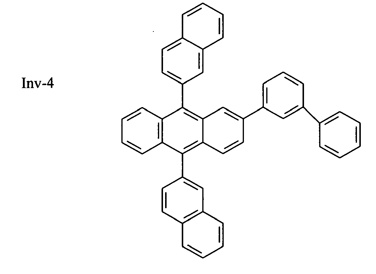
- EL devices Samples 19-23, were fabricated in an identical manner as Sample 1-5, except Inv-1 was replaced with Inv-4.
- Sample 25 was prepared in the same manner as Sample 6.
- the devices thus formed were tested for in the same manner as Samples 1-6, except the devices were tested for stability by operating the cells at 20 mA/cm 2 for 200 h at 70 °C. The testing results are reported in Table 4. Table 4. Evaluation Results for EL devices 19-24.
- the anthracene material of the invention affords a high luminance yield and similar stability relative to a comparison anthracene material when the two materials are compared at similar levels.
- the Inv-4/TBP combination affords a color that is more blue-green than the TBADN/TBP combination and may be desirable for use in a white light-emitting device.
- the anthracene material of the invention affords a high luminance yield and very good operating stability relative to a comparison anthracene material when the two materials are compared at similar levels.
- the Inv-5/TBP combination affords a color that is more blue-green than the TBADN/TBP combination and may be desirable for use in a white light-emitting device.
- EL devices Samples 31-35, were fabricated in an identical manner as Sample 1-5, except Inv-1 was replaced with Inv-7.
- Sample 36 was prepared in the same manner as Sample 6.
- the devices thus formed were tested for in the same manner as Samples 1-6, except the devices were tested for stability by operating the cells at 20 mA/cm 2 for 200 h at 70 °C. The testing results are reported in Table 6. Table 6. Evaluation Results for EL devices 31-36.
- the anthracene material of the invention affords a high luminance yield and similar or better operating stability relative to a comparison anthracene material when the two materials are compared at similar levels.
- the Inv-7/TBP combination affords a color that is more blue-green than the TBADN/TBP combination and may be desirable for use in a white light-emitting device.
- EL devices Samples 37-41, were fabricated in an identical manner as Sample 1-5, except Inv-1 was replaced with Inv-8.
- Sample 42 was prepared in the same manner as Sample 6.
- the devices thus formed were tested for in the same manner as Samples 1-6, except the devices were tested for stability by operating the cells at 20 mA/cm 2 for 200 h at 70 °C. The testing results are reported in Table 7. Table 7. Evaluation Results for EL devices 37-42.
- the anthracene material of the invention affords a high luminance yield and very good operating stability relative to a comparison anthracene material when the two materials are compared at similar levels.
- the Inv-8/TBP combination affords a color that is more blue-green than the TBADN/TBP combination and may be desirable for use in a white light-emitting device.
- the anthracene material of the invention affords a high luminance yield and very good operating stability relative to a comparison anthracene material when the two materials are compared at similar levels.
- the Inv-9/TBP combination affords a color that is more blue-green than the TBADN/TBP combination and may be desirable for use in a white light-emitting device.
Abstract
Claims (15)
- Un dispositif EL comprenant une couche électroluminescente contenant un matériau à base d'anthracène portant au moins un noyau aryle en position 2 et ayant un atome d'hydrogène ou un groupe alkyle en position 6, et ayant jusqu'à 12 noyaux carbocycliques aromatiques contenant au moins un groupe naphtalène en position 9 du groupe anthracène et un groupe aryle en position 10, le matériau à base d'anthracène contenant seulement des noyaux carbocycliques parmi les noyaux, sous réserve que l'anthracène n'ait pas l'une des deux structures


- Dispositif selon la revendication 1, dans lequel le matériau à base d'anthracène comprend 10 noyaux carbocycliques aromatiques contenant seulement des noyaux carbocycliques parmi les noyaux.
- Dispositif selon la revendication 1, dans lequel le matériau à base d'anthracène comprend au moins un groupe 2-naphtyle.
- Dispositif selon la revendication 1, dans lequel le matériau à base d'anthracène comprend des groupes naphtyles choisis séparément en positions 9 et 10.
- Dispositif selon la revendication 4, dans lequel les groupes naphtyles en positions 9 et 10 sont identiques.
- Dispositif selon la revendication 1, dans lequel le matériau à base d'anthracène comprend un groupe biphényle en position 10.
- Dispositif selon la revendication 1, dans lequel la position 6 du matériau à base d'anthracène porte un atome d'hydrogène.
- Dispositif selon la revendication 1, dans lequel le matériau à base d'anthracène comprend seulement un groupe anthracène.
- Dispositif selon la revendication 1, dans lequel le matériau à base d'anthracène est représenté par la formule (1) :
 Ar2 représente un groupe aryle ;Ar9 représente un groupe naphtyle ;Ar10 représente un groupe aryle ;v1, v3, v4, v5, v7, et v8 représentent séparément un atome d'hydrogène ou un substituant ;v6 représente un atome d'hydrogène ou un groupe alkyle.
 - Dispositif selon la revendication 9, dans lequel Ar9 et Ar10 représentent des groupes naphtyles choisis séparément.
- Dispositif selon la revendication 9, dans lequel v6 représente un atome d'hydrogène.
- Dispositif selon la revendication 1, dans lequel la couche électroluminescente contient un matériau de formule (2a) ou (2b),

 Ra - Rh représentent un atome d'hydrogène ou un substituant choisi séparément.
 - Dispositif selon la revendication 1, dans lequel le matériau à base d'anthracène est choisi parmi les matériaux suivants :


- Dispositif selon la revendication 1, comprenant aussi une deuxième couche électroluminescente pour produire une émission de lumière blanche.
- Composé représenté par la formule (1) :
 Ar2 représente un groupe aryle ;Ar9 représente un groupe naphtyle ;Ar10 représente un groupe aryle ;v1, v3, v4, v5, v7, et v8 représentent séparément un atome d'hydrogène ou un substituant ;v6 représente un atome d'hydrogène ou un groupe alkyle ;et sous réserve que 12 noyaux carbocycliques aromatiques au maximum soient présents et comprennent seulement des noyaux carbocycliques parmi les noyaux et sous réserve également que le composé n'ait pas l'une des structures
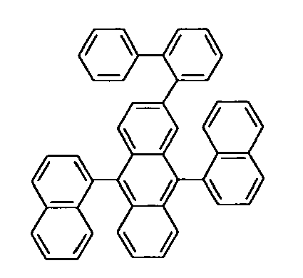
Applications Claiming Priority (2)
| Application Number | Priority Date | Filing Date | Title |
|---|---|---|---|
| US10/809,064 US7326371B2 (en) | 2004-03-25 | 2004-03-25 | Electroluminescent device with anthracene derivative host |
| PCT/US2005/008253 WO2005100506A1 (fr) | 2004-03-25 | 2005-03-11 | Dispositif electroluminescent avec hote derive anthracene |
Publications (3)
| Publication Number | Publication Date |
|---|---|
| EP1730249A1 EP1730249A1 (fr) | 2006-12-13 |
| EP1730249B1 true EP1730249B1 (fr) | 2009-06-17 |
| EP1730249B2 EP1730249B2 (fr) | 2012-12-26 |
Family
ID=34962567
Family Applications (1)
| Application Number | Title | Priority Date | Filing Date |
|---|---|---|---|
| EP05725437A Active EP1730249B2 (fr) | 2004-03-25 | 2005-03-11 | Dispositif electroluminescent avec hote derive anthracene |
Country Status (7)
| Country | Link |
|---|---|
| US (1) | US7326371B2 (fr) |
| EP (1) | EP1730249B2 (fr) |
| JP (2) | JP2007531273A (fr) |
| KR (1) | KR101182702B1 (fr) |
| CN (1) | CN1934215B (fr) |
| DE (1) | DE602005014951D1 (fr) |
| WO (1) | WO2005100506A1 (fr) |
Families Citing this family (136)
| Publication number | Priority date | Publication date | Assignee | Title |
|---|---|---|---|---|
| US20040126617A1 (en) * | 2002-12-31 | 2004-07-01 | Eastman Kodak Company | Efficient electroluminescent device |
| US7329466B2 (en) * | 2004-01-30 | 2008-02-12 | Eastman Kodak Company | Organic element for electroluminescent devices |
| WO2006025700A1 (fr) * | 2004-09-02 | 2006-03-09 | Lg Chem. Ltd. | Derives d'anthracene et dispositif organique electroluminescent les utilisant en tant que materiau electroluminescent |
| US20060204783A1 (en) * | 2005-03-10 | 2006-09-14 | Conley Scott R | Organic electroluminescent device |
| US20060269782A1 (en) * | 2005-05-25 | 2006-11-30 | Eastman Kodak Company | OLED electron-transporting layer |
| US8766023B2 (en) * | 2005-07-20 | 2014-07-01 | Lg Display Co., Ltd. | Synthesis process |
| KR100788254B1 (ko) | 2005-08-16 | 2007-12-27 | (주)그라쎌 | 녹색 발광 화합물 및 이를 발광재료로서 채용하고 있는발광소자 |
| KR100828173B1 (ko) * | 2005-11-22 | 2008-05-08 | (주)그라쎌 | 유기 발광 화합물 및 이를 발광재료로 채용하고 있는 표시소자 |
| US9666826B2 (en) * | 2005-11-30 | 2017-05-30 | Global Oled Technology Llc | Electroluminescent device including an anthracene derivative |
| US20070252517A1 (en) * | 2006-04-27 | 2007-11-01 | Eastman Kodak Company | Electroluminescent device including an anthracene derivative |
| US20070252515A1 (en) * | 2006-04-27 | 2007-11-01 | Eastman Kodak Company | Electroluminescent device including an anthracene derivative |
| KR100893044B1 (ko) * | 2006-07-26 | 2009-04-15 | 주식회사 엘지화학 | 안트라센 유도체, 이를 이용한 유기 전자 소자 및 이 유기전자 소자를 포함하는 전자 장치 |
| JP5003685B2 (ja) * | 2006-11-08 | 2012-08-15 | コニカミノルタホールディングス株式会社 | 表示素子 |
| WO2008056652A1 (fr) * | 2006-11-09 | 2008-05-15 | Idemitsu Kosan Co., Ltd. | Solution contenant un matériau el organique, procédé de synthèse d'un matériau el organique, composé synthétisé par le procédé de synthèse, procédé de formation d'un film mince de matériau el organique, film mince de matériau el organ |
| KR100903203B1 (ko) * | 2006-11-30 | 2009-06-18 | 에스에프씨 주식회사 | 안트라센 유도체 및 이를 채용한 유기전계발광소자 |
| TWI502049B (zh) * | 2006-12-28 | 2015-10-01 | Semiconductor Energy Lab | 有機化合物及合成有機化合物與蒽衍生物之方法 |
| US8795855B2 (en) * | 2007-01-30 | 2014-08-05 | Global Oled Technology Llc | OLEDs having high efficiency and excellent lifetime |
| EP2444470B1 (fr) | 2007-08-31 | 2016-10-26 | Semiconductor Energy Laboratory Co., Ltd. | Élément électroluminescent, dispositif électroluminescent et appareil électronique |
| KR100935356B1 (ko) * | 2007-11-19 | 2010-01-06 | 다우어드밴스드디스플레이머티리얼 유한회사 | 녹색 발광 화합물 및 이를 발광재료로서 채용하고 있는유기 전기 발광 소자 |
| KR100940938B1 (ko) * | 2007-12-04 | 2010-02-08 | 다우어드밴스드디스플레이머티리얼 유한회사 | 신규한 유기 발광 화합물 및 이를 발광재료로서 채용하고있는 유기 전기 발광 소자 |
| JP4662384B2 (ja) * | 2007-12-25 | 2011-03-30 | 財団法人山形県産業技術振興機構 | 有機エレクトロルミネッセンス材料およびそれを用いた素子 |
| KR100974562B1 (ko) * | 2007-12-31 | 2010-08-06 | 다우어드밴스드디스플레이머티리얼 유한회사 | 신규한 유기 발광 화합물 및 이를 발광재료로서 채용하고있는 유기 발광 소자 |
| KR100991416B1 (ko) * | 2007-12-31 | 2010-11-03 | 다우어드밴스드디스플레이머티리얼 유한회사 | 유기 발광 화합물 및 이를 포함하는 유기 발광 소자 |
| KR101001384B1 (ko) * | 2008-02-29 | 2010-12-14 | 다우어드밴스드디스플레이머티리얼 유한회사 | 신규한 유기 발광 화합물 및 이를 발광재료로서 채용하고있는 유기 전기 발광 소자 |
| KR100901887B1 (ko) * | 2008-03-14 | 2009-06-09 | (주)그라쎌 | 신규한 유기 발광 화합물 및 이를 채용하고 있는 유기 발광소자 |
| KR100989815B1 (ko) * | 2008-03-20 | 2010-10-29 | 다우어드밴스드디스플레이머티리얼 유한회사 | 신규한 유기 발광 화합물 및 이를 발광재료로서 채용하고있는 유기 발광 소자 |
| KR100946411B1 (ko) * | 2008-03-28 | 2010-03-09 | 다우어드밴스드디스플레이머티리얼 유한회사 | 신규한 유기 발광 화합물 및 이를 발광재료로서 채용하고있는 유기 발광 소자 |
| KR100910150B1 (ko) * | 2008-04-02 | 2009-08-03 | (주)그라쎌 | 신규한 유기 발광 화합물 및 이를 발광재료로서 채용하고있는 유기 발광 소자 |
| KR101495547B1 (ko) * | 2008-04-17 | 2015-02-25 | 롬엔드하스전자재료코리아유한회사 | 신규한 전자 재료용 화합물 및 이를 포함하는 유기 전자소자 |
| KR20090111915A (ko) * | 2008-04-23 | 2009-10-28 | (주)그라쎌 | 신규한 유기 발광 화합물 및 이를 발광재료로서 채용하고있는 유기 발광 소자 |
| JPWO2009154207A1 (ja) * | 2008-06-17 | 2011-12-01 | 出光興産株式会社 | アントラセン誘導体及びそれを用いた有機エレクトロルミネッセンス素子 |
| KR20100000772A (ko) * | 2008-06-25 | 2010-01-06 | 다우어드밴스드디스플레이머티리얼 유한회사 | 신규한 유기 발광 화합물 및 이를 발광재료로서 채용하고있는 유기 발광 소자 |
| EP2145936A3 (fr) * | 2008-07-14 | 2010-03-17 | Gracel Display Inc. | Dérivés de fluorène et pyrène et dispositif électroluminescent organique les utilisant |
| KR20100041043A (ko) * | 2008-10-13 | 2010-04-22 | 다우어드밴스드디스플레이머티리얼 유한회사 | 신규한 유기 발광 화합물 및 이를 발광재료로서 채용하고 있는 유기 발광 소자 |
| DE102009005746A1 (de) | 2009-01-23 | 2010-07-29 | Merck Patent Gmbh | Materialien für organische Elektrolumineszenzvorrichtungen |
| DE102009009277B4 (de) | 2009-02-17 | 2023-12-07 | Merck Patent Gmbh | Organische elektronische Vorrichtung, Verfahren zu deren Herstellung und Verwendung von Verbindungen |
| KR20100109050A (ko) * | 2009-03-31 | 2010-10-08 | 다우어드밴스드디스플레이머티리얼 유한회사 | 신규한 유기 발광 화합물 및 이를 포함하는 유기 전계 발광소자 |
| US9153790B2 (en) * | 2009-05-22 | 2015-10-06 | Idemitsu Kosan Co., Ltd. | Organic electroluminescent device |
| KR101754445B1 (ko) * | 2009-05-29 | 2017-07-05 | 이데미쓰 고산 가부시키가이샤 | 안트라센 유도체 및 그것을 이용한 유기 전계 발광 소자 |
| US20120104380A1 (en) | 2009-06-22 | 2012-05-03 | Merck Patent Gmbh | Conducting formulation |
| US8877356B2 (en) * | 2009-07-22 | 2014-11-04 | Global Oled Technology Llc | OLED device with stabilized yellow light-emitting layer |
| EP2462203B1 (fr) | 2009-08-04 | 2016-03-02 | Merck Patent GmbH | Dispositifs électroniques comprenant des hydrocarbures polycycliques |
| DE102009042693A1 (de) | 2009-09-23 | 2011-03-24 | Merck Patent Gmbh | Materialien für elektronische Vorrichtungen |
| US8716699B2 (en) * | 2009-10-29 | 2014-05-06 | E I Du Pont De Nemours And Company | Organic light-emitting diodes having white light emission |
| US8716700B2 (en) * | 2009-10-29 | 2014-05-06 | E I Du Pont De Nemours And Company | Organic light-emitting diodes having white light emission |
| DE102009053191A1 (de) | 2009-11-06 | 2011-05-12 | Merck Patent Gmbh | Materialien für elektronische Vorrichtungen |
| JP5897472B2 (ja) | 2009-12-22 | 2016-03-30 | メルク パテント ゲーエムベーハー | エレクトロルミネセンス機能性界面活性剤 |
| EP2517275B1 (fr) | 2009-12-22 | 2018-11-07 | Merck Patent GmbH | Formulations comprenant des matériaux fonctionnels à phases séparées |
| WO2011076314A1 (fr) | 2009-12-22 | 2011-06-30 | Merck Patent Gmbh | Formulations électroluminescentes |
| CN102668152A (zh) | 2009-12-23 | 2012-09-12 | 默克专利有限公司 | 包括聚合粘结剂的组合物 |
| JP5840621B2 (ja) | 2009-12-23 | 2016-01-06 | メルク パテント ゲーエムベーハー | 有機半導体化合物を含む組成物 |
| DE102010005697A1 (de) | 2010-01-25 | 2011-07-28 | Merck Patent GmbH, 64293 | Verbindungen für elektronische Vorrichtungen |
| DE102010009193B4 (de) | 2010-02-24 | 2022-05-19 | MERCK Patent Gesellschaft mit beschränkter Haftung | Zusammensetzung enthaltend Fluor-Fluor Assoziate, Verfahren zu deren Herstellung, deren Verwendung sowie organische elektronische Vorrichtung diese enthaltend |
| DE102010009903A1 (de) | 2010-03-02 | 2011-09-08 | Merck Patent Gmbh | Verbindungen für elektronische Vorrichtungen |
| JP2013522816A (ja) | 2010-03-11 | 2013-06-13 | メルク パテント ゲーエムベーハー | 発光ファイバー |
| KR20130020883A (ko) | 2010-03-11 | 2013-03-04 | 메르크 파텐트 게엠베하 | 요법 및 미용에서의 섬유 |
| DE102010013068A1 (de) | 2010-03-26 | 2011-09-29 | Merck Patent Gmbh | Verbindungen für elektronische Vorrichtungen |
| EP2559079B1 (fr) | 2010-04-12 | 2020-04-01 | Merck Patent GmbH | Composition et procédé pour la préparation de dispositifs électroniques organiques |
| CN102859738B (zh) | 2010-04-12 | 2016-08-03 | 默克专利有限公司 | 具有改进的性能的组合物 |
| WO2011147522A1 (fr) | 2010-05-27 | 2011-12-01 | Merck Patent Gmbh | Composition comprenant des points quantiques |
| EP2576724B1 (fr) | 2010-05-27 | 2019-04-24 | Merck Patent GmbH | Procédé pour la préparation de dispositifs électroniques organiques |
| DE102010024335A1 (de) | 2010-06-18 | 2011-12-22 | Merck Patent Gmbh | Verbindungen für elektronische Vorrichtungen |
| DE102010024542A1 (de) | 2010-06-22 | 2011-12-22 | Merck Patent Gmbh | Materialien für elektronische Vorrichtungen |
| US20130226268A1 (en) | 2010-07-26 | 2013-08-29 | Merck Patent Gmbh | Nanocrystals in devices |
| WO2012013272A1 (fr) | 2010-07-26 | 2012-02-02 | Merck Patent Gmbh | Boîtes quantiques et hôtes |
| DE102010033548A1 (de) | 2010-08-05 | 2012-02-09 | Merck Patent Gmbh | Materialien für elektronische Vorrichtungen |
| DE102010048074A1 (de) | 2010-10-09 | 2012-04-12 | Merck Patent Gmbh | Materialien für elektronische Vorrichtungen |
| DE102010048607A1 (de) | 2010-10-15 | 2012-04-19 | Merck Patent Gmbh | Verbindungen für elektronische Vorrichtungen |
| US9627626B2 (en) | 2011-01-13 | 2017-04-18 | Merck Patent Gmbh | Compounds for organic electroluminescent devices |
| US9492681B2 (en) | 2011-02-14 | 2016-11-15 | Merck Patent Gmbh | Device and method for treatment of cells and cell tissue |
| DE102011011539A1 (de) | 2011-02-17 | 2012-08-23 | Merck Patent Gmbh | Verbindungen für elektronische Vorrichtungen |
| WO2012126566A1 (fr) | 2011-03-24 | 2012-09-27 | Merck Patent Gmbh | Matériaux fonctionnels ioniques organiques |
| JP6271417B2 (ja) | 2011-04-13 | 2018-01-31 | メルク パテント ゲーエムベーハー | 電子素子のための材料 |
| WO2012139693A1 (fr) | 2011-04-13 | 2012-10-18 | Merck Patent Gmbh | Composés pour dispositifs électroniques |
| WO2012143079A1 (fr) | 2011-04-18 | 2012-10-26 | Merck Patent Gmbh | Composés pour des dispositifs électroniques |
| WO2012149992A1 (fr) | 2011-05-04 | 2012-11-08 | Merck Patent Gmbh | Dispositif de conservation de produits frais |
| WO2012152366A1 (fr) | 2011-05-12 | 2012-11-15 | Merck Patent Gmbh | Composés ioniques organiques, compositions et dispositifs électroniques |
| JP6223984B2 (ja) | 2011-10-27 | 2017-11-01 | メルク パテント ゲーエムベーハー | 電子素子のための材料 |
| KR20140123555A (ko) | 2012-01-30 | 2014-10-22 | 메르크 파텐트 게엠베하 | 파이버 상의 나노결정 |
| KR102015765B1 (ko) | 2012-02-14 | 2019-10-21 | 메르크 파텐트 게엠베하 | 유기 전계발광 소자용 스피로비플루오렌 화합물 |
| JP2013207139A (ja) * | 2012-03-29 | 2013-10-07 | Kaneka Corp | 発光材料および有機el素子 |
| US20160301003A1 (en) | 2013-12-06 | 2016-10-13 | Merck Patent Gmbh | Compositions containing a polymeric binder which comprises acrylic and/or methacrylic acid ester units |
| JP6695863B2 (ja) | 2014-09-05 | 2020-05-20 | メルク パテント ゲーエムベーハー | 調合物と電子素子 |
| WO2016107663A1 (fr) | 2014-12-30 | 2016-07-07 | Merck Patent Gmbh | Formulations et dispositifs électroniques |
| EP3251128B1 (fr) | 2015-01-30 | 2023-06-14 | Merck Patent GmbH | Formulations comprenant une proportion faible de particules |
| JP6800879B2 (ja) | 2015-03-30 | 2020-12-16 | メルク パテント ゲーエムベーハー | シロキサン溶媒を含む有機機能性材料の調合物 |
| EP3581633B1 (fr) | 2015-06-12 | 2021-01-27 | Merck Patent GmbH | Esters contenant des cycles non aromatiques en tant que solvants pour des formulations de diodes électroluminescentes organiques (oled) |
| US20180212166A1 (en) | 2015-07-15 | 2018-07-26 | Merck Patent Gmbh | Composition comprising organic semiconducting compounds |
| WO2017036572A1 (fr) | 2015-08-28 | 2017-03-09 | Merck Patent Gmbh | Formulation d'un matériau fonctionnel organique comprenant un solvant contenant un groupe époxy |
| EP3147961A1 (fr) * | 2015-09-28 | 2017-03-29 | Novaled GmbH | Dispositif électroluminescent organique |
| US11005042B2 (en) | 2015-12-10 | 2021-05-11 | Merck Patent Gmbh | Formulations containing ketones comprising non-aromatic cycles |
| JP7051684B2 (ja) | 2015-12-15 | 2022-04-11 | メルク パテント ゲーエムベーハー | 有機電子調合物のための溶媒として芳香族基を含むエステル |
| KR20180095028A (ko) | 2015-12-16 | 2018-08-24 | 메르크 파텐트 게엠베하 | 둘 이상의 상이한 용매의 혼합물을 함유하는 제형 |
| KR20180096676A (ko) | 2015-12-16 | 2018-08-29 | 메르크 파텐트 게엠베하 | 고체 용매를 함유하는 제형 |
| KR20180110125A (ko) | 2016-02-17 | 2018-10-08 | 메르크 파텐트 게엠베하 | 유기 기능성 재료의 제형 |
| DE102016003104A1 (de) | 2016-03-15 | 2017-09-21 | Merck Patent Gmbh | Behälter umfassend eine Formulierung enthaltend mindestens einen organischen Halbleiter |
| WO2017194435A1 (fr) | 2016-05-11 | 2017-11-16 | Merck Patent Gmbh | Compositions pour cellules électrochimiques |
| KR20190019138A (ko) | 2016-06-16 | 2019-02-26 | 메르크 파텐트 게엠베하 | 유기 기능성 재료의 제형 |
| KR102374183B1 (ko) | 2016-06-17 | 2022-03-14 | 메르크 파텐트 게엠베하 | 유기 기능성 재료의 제형 |
| TW201815998A (zh) | 2016-06-28 | 2018-05-01 | 德商麥克專利有限公司 | 有機功能材料之調配物 |
| JP6980757B2 (ja) | 2016-08-04 | 2021-12-15 | メルク パテント ゲーエムベーハー | 有機機能材料の調合物 |
| JP7046938B2 (ja) | 2016-10-31 | 2022-04-04 | メルク パテント ゲーエムベーハー | 有機機能材料の調合物 |
| US10950792B2 (en) | 2016-10-31 | 2021-03-16 | Merck Patent Gmbh | Formulation of an organic functional material |
| TWI756292B (zh) | 2016-11-14 | 2022-03-01 | 德商麥克專利有限公司 | 具有受體基團與供體基團之化合物 |
| US10892414B2 (en) | 2016-12-06 | 2021-01-12 | Merck Patent Gmbh | Process for making electronic device |
| JP7091337B2 (ja) | 2016-12-13 | 2022-06-27 | メルク パテント ゲーエムベーハー | 有機機能材料の調合物 |
| US20200098996A1 (en) | 2016-12-22 | 2020-03-26 | Merck Patent Gmbh | Mixtures comprising at least two organofunctional compounds |
| TWI763772B (zh) | 2017-01-30 | 2022-05-11 | 德商麥克專利有限公司 | 電子裝置之有機元件的形成方法 |
| TWI791481B (zh) | 2017-01-30 | 2023-02-11 | 德商麥克專利有限公司 | 形成有機電致發光(el)元件之方法 |
| KR20190131554A (ko) | 2017-03-31 | 2019-11-26 | 메르크 파텐트 게엠베하 | 유기 발광 다이오드 (oled) 를 위한 인쇄 방법 |
| WO2018189050A1 (fr) | 2017-04-10 | 2018-10-18 | Merck Patent Gmbh | Formulation d'un matériau fonctionnel organique |
| US11581487B2 (en) | 2017-04-26 | 2023-02-14 | Oti Lumionics Inc. | Patterned conductive coating for surface of an opto-electronic device |
| WO2018202603A1 (fr) | 2017-05-03 | 2018-11-08 | Merck Patent Gmbh | Formulation d'un matériau fonctionnel organique |
| TWI813576B (zh) | 2017-07-03 | 2023-09-01 | 德商麥克專利有限公司 | 具有低含量苯酚類雜質的調配物 |
| WO2019016184A1 (fr) | 2017-07-18 | 2019-01-24 | Merck Patent Gmbh | Formulation d'un matériau fonctionnel organique |
| KR102072922B1 (ko) | 2017-10-30 | 2020-02-10 | 주식회사 엘지화학 | 헤테로고리 화합물 및 이를 포함하는 유기 발광 소자 |
| KR102186088B1 (ko) | 2017-11-16 | 2020-12-03 | 주식회사 엘지화학 | 다환 화합물 및 이를 포함한 유기 발광 소자 |
| WO2019115573A1 (fr) | 2017-12-15 | 2019-06-20 | Merck Patent Gmbh | Formulation d'un matériau fonctionnel organique |
| US11751415B2 (en) | 2018-02-02 | 2023-09-05 | Oti Lumionics Inc. | Materials for forming a nucleation-inhibiting coating and devices incorporating same |
| KR20200125660A (ko) | 2018-02-26 | 2020-11-04 | 메르크 파텐트 게엠베하 | 유기 기능성 재료의 포뮬레이션 |
| EP3807367B1 (fr) | 2018-06-15 | 2023-07-19 | Merck Patent GmbH | Formulation d'un matériau fonctionnel organique |
| CN112740432A (zh) | 2018-09-24 | 2021-04-30 | 默克专利有限公司 | 用于生产粒状材料的方法 |
| TW202034551A (zh) | 2018-11-06 | 2020-09-16 | 德商麥克專利有限公司 | 用於形成電子裝置的有機元件之方法 |
| US11780829B2 (en) | 2019-01-30 | 2023-10-10 | The University Of Southern California | Organic electroluminescent materials and devices |
| US11812624B2 (en) * | 2019-01-30 | 2023-11-07 | The University Of Southern California | Organic electroluminescent materials and devices |
| CN113785411B (zh) | 2019-03-07 | 2023-04-11 | Oti照明公司 | 用于形成成核抑制涂层的材料和结合所述成核抑制涂层的装置 |
| JP2021103714A (ja) * | 2019-12-25 | 2021-07-15 | 出光興産株式会社 | 有機エレクトロルミネッセンス素子及び電子機器 |
| TW202214791A (zh) | 2020-04-21 | 2022-04-16 | 德商麥克專利有限公司 | 有機功能性材料之調配物 |
| WO2021213917A1 (fr) | 2020-04-21 | 2021-10-28 | Merck Patent Gmbh | Émulsions comprenant des matériaux fonctionnels organiques |
| EP4169082A1 (fr) | 2020-06-23 | 2023-04-26 | Merck Patent GmbH | Procédé de production d'un mélange |
| WO2022122607A1 (fr) | 2020-12-08 | 2022-06-16 | Merck Patent Gmbh | Système d'encre et procédé d'impression à jet d'encre |
| JP2024515366A (ja) | 2021-04-23 | 2024-04-09 | メルク パテント ゲーエムベーハー | 有機機能材料の調合物 |
| CN117355364A (zh) | 2021-05-21 | 2024-01-05 | 默克专利有限公司 | 用于连续纯化至少一种功能材料的方法和用于连续纯化至少一种功能材料的装置 |
| WO2023012084A1 (fr) | 2021-08-02 | 2023-02-09 | Merck Patent Gmbh | Procédé d'impression par combinaison d'encres |
| TW202349760A (zh) | 2021-10-05 | 2023-12-16 | 德商麥克專利有限公司 | 電子裝置之有機元件的形成方法 |
| WO2023237458A1 (fr) | 2022-06-07 | 2023-12-14 | Merck Patent Gmbh | Procédé d'impression d'une couche fonctionnelle d'un dispositif électronique par combinaison d'encres |
Family Cites Families (22)
| Publication number | Priority date | Publication date | Assignee | Title |
|---|---|---|---|---|
| JP3588978B2 (ja) | 1997-06-12 | 2004-11-17 | 凸版印刷株式会社 | 有機薄膜el素子 |
| JP3148176B2 (ja) | 1998-04-15 | 2001-03-19 | 日本電気株式会社 | 有機エレクトロルミネッセンス素子 |
| US6582837B1 (en) | 1997-07-14 | 2003-06-24 | Nec Corporation | Organic electroluminescence device |
| US5972247A (en) | 1998-03-20 | 1999-10-26 | Eastman Kodak Company | Organic electroluminescent elements for stable blue electroluminescent devices |
| JP3769933B2 (ja) | 1998-05-20 | 2006-04-26 | 凸版印刷株式会社 | 発光材料及び有機薄膜el素子 |
| JP2000053676A (ja) * | 1998-08-10 | 2000-02-22 | Idemitsu Kosan Co Ltd | 芳香族炭化水素化合物およびそれを用いた有機エレクトロルミネッセンス素子 |
| US6361886B2 (en) * | 1998-12-09 | 2002-03-26 | Eastman Kodak Company | Electroluminescent device with improved hole transport layer |
| TW484341B (en) * | 1999-08-03 | 2002-04-21 | Sumitomo Chemical Co | Polymeric fluorescent substance and polymer light emitting device |
| US6361887B1 (en) * | 1999-10-20 | 2002-03-26 | Eastman Kodak Company | Electroluminescent devices having naphthylanthracene-based polymers |
| KR100329571B1 (ko) * | 2000-03-27 | 2002-03-23 | 김순택 | 유기 전자 발광소자 |
| US6998487B2 (en) | 2001-04-27 | 2006-02-14 | Lg Chem, Ltd. | Double-spiro organic compounds and organic electroluminescent devices using the same |
| KR100691543B1 (ko) * | 2002-01-18 | 2007-03-09 | 주식회사 엘지화학 | 새로운 전자 수송용 물질 및 이를 이용한 유기 발광 소자 |
| US6670053B2 (en) * | 2002-02-26 | 2003-12-30 | Eastman Kodak Company | Organic electroluminescent devices with high luminance |
| US6661023B2 (en) * | 2002-02-28 | 2003-12-09 | Eastman Kodak Company | Organic element for electroluminescent devices |
| US20040001969A1 (en) * | 2002-06-27 | 2004-01-01 | Eastman Kodak Company | Device containing green organic light-emitting diode |
| JP4025136B2 (ja) | 2002-07-31 | 2007-12-19 | 出光興産株式会社 | アントラセン誘導体、有機エレクトロルミネッセンス素子用発光材料及び有機エレクトロルミネッセンス素子 |
| US7839074B2 (en) | 2002-08-23 | 2010-11-23 | Idemitsu Kosan Co., Ltd. | Organic electroluminescence device and anthracene derivative |
| US6828044B2 (en) * | 2002-10-25 | 2004-12-07 | Eastman Kodak Company | Dopant in an electroluminescent device |
| US20050058853A1 (en) * | 2003-09-15 | 2005-03-17 | Eastman Kodak Company | Green organic light-emitting diodes |
| JP2005170911A (ja) * | 2003-12-15 | 2005-06-30 | Idemitsu Kosan Co Ltd | 芳香族化合物およびそれを用いた有機エレクトロルミネッセンス素子 |
| US7252893B2 (en) * | 2004-02-17 | 2007-08-07 | Eastman Kodak Company | Anthracene derivative host having ranges of dopants |
| US7033681B2 (en) * | 2004-03-18 | 2006-04-25 | Eastman Kodak Company | Organic element for electroluminescent devices |
-
2004
- 2004-03-25 US US10/809,064 patent/US7326371B2/en active Active
-
2005
- 2005-03-11 CN CN2005800094046A patent/CN1934215B/zh active Active
- 2005-03-11 KR KR1020067019642A patent/KR101182702B1/ko active IP Right Grant
- 2005-03-11 DE DE602005014951T patent/DE602005014951D1/de active Active
- 2005-03-11 EP EP05725437A patent/EP1730249B2/fr active Active
- 2005-03-11 WO PCT/US2005/008253 patent/WO2005100506A1/fr not_active Application Discontinuation
- 2005-03-11 JP JP2007504998A patent/JP2007531273A/ja active Pending
-
2011
- 2011-12-20 JP JP2011278389A patent/JP5744713B2/ja active Active
Also Published As
| Publication number | Publication date |
|---|---|
| JP2012104842A (ja) | 2012-05-31 |
| US7326371B2 (en) | 2008-02-05 |
| WO2005100506A1 (fr) | 2005-10-27 |
| EP1730249B2 (fr) | 2012-12-26 |
| CN1934215A (zh) | 2007-03-21 |
| JP2007531273A (ja) | 2007-11-01 |
| KR101182702B1 (ko) | 2012-09-13 |
| KR20060134999A (ko) | 2006-12-28 |
| JP5744713B2 (ja) | 2015-07-08 |
| US20050211958A1 (en) | 2005-09-29 |
| EP1730249A1 (fr) | 2006-12-13 |
| CN1934215B (zh) | 2010-08-18 |
| DE602005014951D1 (de) | 2009-07-30 |
Similar Documents
| Publication | Publication Date | Title |
|---|---|---|
| EP1730249B1 (fr) | Dispositif electroluminescent avec hote derive anthracene | |
| EP1911069B1 (fr) | Element electroluminescent organique a faible tension | |
| EP1941562B1 (fr) | Element organique pour dispositifs electroluminescents a faible tension | |
| EP1891692B1 (fr) | Element organique pour dispositifs electroluminescents a basse tension | |
| EP1941563B1 (fr) | Element organique pour dispositifs electroluminescents a faible tension | |
| EP1955384B1 (fr) | Dispositif electroluminescent contenant un derive d'anthracene | |
| EP1807482B1 (fr) | Element organique pour dispositifs electroluminescents | |
| EP1955385B1 (fr) | Dispositif electroluminescent contenant un derive de phenanthroline | |
| KR101146268B1 (ko) | 전기발광 디바이스용 유기 소자 | |
| US20060019116A1 (en) | White electroluminescent device with anthracene derivative host | |
| EP1730250A1 (fr) | Element organique pour dispositifs electroluminescents | |
| WO2007050331A1 (fr) | Element organique pour dispositifs electroluminescents a faible tension | |
| WO2007050303A1 (fr) | Element organique pour dispositifs electroluminescents a faible tension | |
| EP1940997A1 (fr) | Element organique pour dispositfs electroluminescents a faible tension | |
| US20060286402A1 (en) | Organic element for low voltage electroluminescent devices | |
| WO2005075599A1 (fr) | Element organique pour dispositifs electroluminescents | |
| WO2007005252A1 (fr) | Dispositifs electroluminescents avec ligands bidentes d’azote | |
| US7033681B2 (en) | Organic element for electroluminescent devices | |
| US7195829B2 (en) | Organic element for electroluminescent devices | |
| WO2005093871A1 (fr) | Reduction de la temperature de sublimation par fluoration de derives de rubrene utilises dans des dispositifs electroluminescents organiques |
Legal Events
| Date | Code | Title | Description |
|---|---|---|---|
| PUAI | Public reference made under article 153(3) epc to a published international application that has entered the european phase |
Free format text: ORIGINAL CODE: 0009012 |
|
| 17P | Request for examination filed |
Effective date: 20060823 |
|
| AK | Designated contracting states |
Kind code of ref document: A1 Designated state(s): DE FR GB |
|
| RIN1 | Information on inventor provided before grant (corrected) |
Inventor name: CONLEY, SCOTT, ROBERT Inventor name: COSIMBESCU, LELIA Inventor name: VREELAND, WILLIAM, BERNARD |
|
| DAX | Request for extension of the european patent (deleted) | ||
| RBV | Designated contracting states (corrected) |
Designated state(s): DE FR GB |
|
| 17Q | First examination report despatched |
Effective date: 20070215 |
|
| GRAP | Despatch of communication of intention to grant a patent |
Free format text: ORIGINAL CODE: EPIDOSNIGR1 |
|
| GRAJ | Information related to disapproval of communication of intention to grant by the applicant or resumption of examination proceedings by the epo deleted |
Free format text: ORIGINAL CODE: EPIDOSDIGR1 |
|
| GRAJ | Information related to disapproval of communication of intention to grant by the applicant or resumption of examination proceedings by the epo deleted |
Free format text: ORIGINAL CODE: EPIDOSDIGR1 |
|
| GRAP | Despatch of communication of intention to grant a patent |
Free format text: ORIGINAL CODE: EPIDOSNIGR1 |
|
| GRAJ | Information related to disapproval of communication of intention to grant by the applicant or resumption of examination proceedings by the epo deleted |
Free format text: ORIGINAL CODE: EPIDOSDIGR1 |
|
| GRAP | Despatch of communication of intention to grant a patent |
Free format text: ORIGINAL CODE: EPIDOSNIGR1 |
|
| GRAS | Grant fee paid |
Free format text: ORIGINAL CODE: EPIDOSNIGR3 |
|
| GRAA | (expected) grant |
Free format text: ORIGINAL CODE: 0009210 |
|
| AK | Designated contracting states |
Kind code of ref document: B1 Designated state(s): DE FR GB |
|
| REG | Reference to a national code |
Ref country code: GB Ref legal event code: FG4D |
|
| REF | Corresponds to: |
Ref document number: 602005014951 Country of ref document: DE Date of ref document: 20090730 Kind code of ref document: P |
|
| PLBI | Opposition filed |
Free format text: ORIGINAL CODE: 0009260 |
|
| PLAX | Notice of opposition and request to file observation + time limit sent |
Free format text: ORIGINAL CODE: EPIDOSNOBS2 |
|
| 26 | Opposition filed |
Opponent name: MERCK KGAA Effective date: 20100316 |
|
| RAP2 | Party data changed (patent owner data changed or rights of a patent transferred) |
Owner name: GLOBAL OLED TECHNOLOGY LLC |
|
| PLAF | Information modified related to communication of a notice of opposition and request to file observations + time limit |
Free format text: ORIGINAL CODE: EPIDOSCOBS2 |
|
| PLBB | Reply of patent proprietor to notice(s) of opposition received |
Free format text: ORIGINAL CODE: EPIDOSNOBS3 |
|
| REG | Reference to a national code |
Ref country code: GB Ref legal event code: 732E Free format text: REGISTERED BETWEEN 20110224 AND 20110302 |
|
| RAP2 | Party data changed (patent owner data changed or rights of a patent transferred) |
Owner name: GLOBAL OLED TECHNOLOGY LLC |
|
| RIC2 | Information provided on ipc code assigned after grant |
Ipc: H01L 51/00 20060101AFI20120329BHEP Ipc: C09K 11/06 20060101ALI20120329BHEP Ipc: H01L 51/30 20060101ALI20120329BHEP Ipc: H05B 33/14 20060101ALI20120329BHEP |
|
| PUAH | Patent maintained in amended form |
Free format text: ORIGINAL CODE: 0009272 |
|
| STAA | Information on the status of an ep patent application or granted ep patent |
Free format text: STATUS: PATENT MAINTAINED AS AMENDED |
|
| 27A | Patent maintained in amended form |
Effective date: 20121226 |
|
| AK | Designated contracting states |
Kind code of ref document: B2 Designated state(s): DE FR GB |
|
| REG | Reference to a national code |
Ref country code: DE Ref legal event code: R102 Ref document number: 602005014951 Country of ref document: DE Effective date: 20121226 |
|
| REG | Reference to a national code |
Ref country code: FR Ref legal event code: PLFP Year of fee payment: 12 |
|
| REG | Reference to a national code |
Ref country code: FR Ref legal event code: PLFP Year of fee payment: 13 |
|
| REG | Reference to a national code |
Ref country code: FR Ref legal event code: PLFP Year of fee payment: 14 |
|
| PGFP | Annual fee paid to national office [announced via postgrant information from national office to epo] |
Ref country code: FR Payment date: 20230322 Year of fee payment: 19 |
|
| PGFP | Annual fee paid to national office [announced via postgrant information from national office to epo] |
Ref country code: GB Payment date: 20230321 Year of fee payment: 19 Ref country code: DE Payment date: 20220620 Year of fee payment: 19 |