EP1689220A2 - Wärmeabfuhranordnung und Verfahren in einer elektronischen Vorrichtung - Google Patents
Wärmeabfuhranordnung und Verfahren in einer elektronischen Vorrichtung Download PDFInfo
- Publication number
- EP1689220A2 EP1689220A2 EP05108116A EP05108116A EP1689220A2 EP 1689220 A2 EP1689220 A2 EP 1689220A2 EP 05108116 A EP05108116 A EP 05108116A EP 05108116 A EP05108116 A EP 05108116A EP 1689220 A2 EP1689220 A2 EP 1689220A2
- Authority
- EP
- European Patent Office
- Prior art keywords
- shielding case
- circuit board
- heat sink
- heat
- holding panels
- Prior art date
- Legal status (The legal status is an assumption and is not a legal conclusion. Google has not performed a legal analysis and makes no representation as to the accuracy of the status listed.)
- Withdrawn
Links
- 238000000034 method Methods 0.000 title claims description 6
- 238000003825 pressing Methods 0.000 claims description 3
- 238000005452 bending Methods 0.000 claims 1
- 230000005855 radiation Effects 0.000 description 6
- 230000009471 action Effects 0.000 description 4
- 230000000694 effects Effects 0.000 description 4
- 230000000994 depressogenic effect Effects 0.000 description 3
- 230000002349 favourable effect Effects 0.000 description 3
- 230000004048 modification Effects 0.000 description 3
- 238000012986 modification Methods 0.000 description 3
- 230000008878 coupling Effects 0.000 description 2
- 238000010168 coupling process Methods 0.000 description 2
- 238000005859 coupling reaction Methods 0.000 description 2
- 238000004519 manufacturing process Methods 0.000 description 2
- 239000007769 metal material Substances 0.000 description 2
- 239000004020 conductor Substances 0.000 description 1
- 238000010276 construction Methods 0.000 description 1
- 238000010586 diagram Methods 0.000 description 1
- 238000001125 extrusion Methods 0.000 description 1
- 230000006872 improvement Effects 0.000 description 1
- 230000010354 integration Effects 0.000 description 1
- 239000004973 liquid crystal related substance Substances 0.000 description 1
- 230000004044 response Effects 0.000 description 1
Images



Classifications
-
- H—ELECTRICITY
- H05—ELECTRIC TECHNIQUES NOT OTHERWISE PROVIDED FOR
- H05K—PRINTED CIRCUITS; CASINGS OR CONSTRUCTIONAL DETAILS OF ELECTRIC APPARATUS; MANUFACTURE OF ASSEMBLAGES OF ELECTRICAL COMPONENTS
- H05K7/00—Constructional details common to different types of electric apparatus
- H05K7/20—Modifications to facilitate cooling, ventilating, or heating
-
- H—ELECTRICITY
- H05—ELECTRIC TECHNIQUES NOT OTHERWISE PROVIDED FOR
- H05K—PRINTED CIRCUITS; CASINGS OR CONSTRUCTIONAL DETAILS OF ELECTRIC APPARATUS; MANUFACTURE OF ASSEMBLAGES OF ELECTRICAL COMPONENTS
- H05K7/00—Constructional details common to different types of electric apparatus
- H05K7/20—Modifications to facilitate cooling, ventilating, or heating
- H05K7/2039—Modifications to facilitate cooling, ventilating, or heating characterised by the heat transfer by conduction from the heat generating element to a dissipating body
- H05K7/20436—Inner thermal coupling elements in heat dissipating housings, e.g. protrusions or depressions integrally formed in the housing
- H05K7/2049—Pressing means used to urge contact, e.g. springs
-
- H—ELECTRICITY
- H05—ELECTRIC TECHNIQUES NOT OTHERWISE PROVIDED FOR
- H05K—PRINTED CIRCUITS; CASINGS OR CONSTRUCTIONAL DETAILS OF ELECTRIC APPARATUS; MANUFACTURE OF ASSEMBLAGES OF ELECTRICAL COMPONENTS
- H05K9/00—Screening of apparatus or components against electric or magnetic fields
Definitions
- the present invention relates to an electronic device such as a digital television broadcast receiving apparatus and particularly to improvement of a heat radiating apparatus and a heat radiating method for radiating the heat generated by its circuit components.
- a conventional digital broadcast receiving apparatus for receiving digital TV signals is required to conduct high-speed processing, particularly of the digital video data.
- the digital TV broadcast receiving apparatus must include a scheme for radiating the heat.
- Jpn. Pat. Appln. KOKAI Publication No. 9-64582 Disclosed in Jpn. Pat. Appln. KOKAI Publication No. 9-64582 is an arrangement in which a shielding case has a planer surface provided with a through hole parallel to its circuit board surface and a separate metallic strip is installed around the through hole in direct contact with each heat generating component mounted on the circuit board.
- the separate metallic strip is attached to the shielding case with a pair of its projections clamping the inner edge at the through hole from both sides along the thicknesswise direction, the projections projecting in parallel to the shielding case surface.
- a shielding case has a planer surface thereof provided with a through hole parallel to its circuit board surface and a cover member is installed around the through hole in direct contact with each heat generating component surface mounted on the circuit board.
- the cover member is attached by an elasticity aided cam construction to the inner edge at the through hole of the shielding case.
- the present invention has been achieved in view of the foregoing problems and its object is to provide a heat radiating apparatus and a heat radiating method which can ensure a favorable degree of heat radiation with the use of a simple arrangement as is feasible in actual use.
- a heat radiating apparatus in an electronic device comprising: a circuit board on which a circuit component is mounted; a heat conductive sheet attached to the circuit component; a shielding case having a flat panel arranged substantially parallel to the surface of the circuit board and holding panels thereof arranged at locations substantially opposite to the circuit component to extend from the base panel towards the circuit board so as to cover the surface of the circuit board including the circuit component; and a heat sink attached to the holding panels of the shielding case, the heat sink coming into direct contact with the heat conductive sheet when the circuit board is covered with the shielding case.
- a heat radiating method for an electronic device comprising: a first step of attaching a heat conductive sheet on a circuit component mounted on a circuit board; a second step of attaching a heat sink to holding panels of a shielding case which are arranged at locations substantially opposite to the circuit component to extend towards the circuit board from a flat panel of the shielding case which extends substantially parallel to the circuit board, the shielding case provided for covering the surface of the circuit board including the circuit board; and a third step of covering the surface of the circuit board with the shielding case such that the heat sink comes into direct contact with the heat conductive sheet.
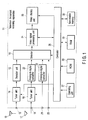
- FIG. 1 schematically illustrates a video signal processing system of a television broadcast receiving apparatus 11 according to the embodiment. More specifically, a digital television broadcast signal is received by a digital television broadcast receiving antenna 12 and transferred via an input terminal 13 to a tuner unit 14.
- the tuner unit 14 is provided for selectively demodulating the input digital television broadcast signal at a desired channel.
- a demodulated signal output from the tuner unit 14 is supplied to a decoder unit 15 where it is decoded, e.g., to a moving picture experts group (MPEG) -2 signal which is then supplied to a selector 16.
- MPEG moving picture experts group
- An analog television broadcast signal received by an analog television broadcast receiving antenna 17 is transferred via an input terminal 18 to a tuner unit 19.
- the tuner unit 19 is provided for selectively demodulating the input analog television broadcast signal at a desired channel.
- a demodulated signal output from the tuner unit 19 is digitized by an analog-to-digital converter 20 before being output to the selector 16.
- An analog video signal supplied to an analog video signal external input terminal 21 is digitized by an analog-to-digital converter 22, and output to the selector 16. Similarly, a digital video signal supplied to a digital video signal external input terminal 23 is directly supplied to the selector 16.
- the selector 16 is provided for selecting one of the four input digital video signals and transmitting the same to a video signal processing unit 24.
- the input digital video signal is subjected to a signal processing of the digital signal processing unit 24 and transferred to a video display unit 25 for display.
- the video display unit 25 may be implemented by, for example, a flat panel display such as a liquid crystal display or a plasma display.
- the fundamental actions of the television broadcast receiving apparatus 11 including the above-described receiving actions are totally controlled by a controller 26.
- the controller 26 is a microprocessor incorporating a central processing unit (CPU) for controlling the action of each component in response to operating information received from an operating unit 27 such as a remote controller (not shown).
- CPU central processing unit
- the controller 26 utilizes a read only memory (ROM) 28 in which the control programs to be executed by the CPU are stored, a random access memory (RAM) 29 to provide a working area for the CPU, and a non-volatile memory 30 in which a variety of setting and controlling information is stored.
- ROM read only memory
- RAM random access memory
- FIG. 2 illustrates a circuit board 31 on which the video signal processing system of the television broadcast receiving apparatus 11 is assembled.
- a plurality of circuit components and circuit patterns is mounted on the circuit board 31 for constructing the video signal processing system.
- an LSI 32 constituting the decoder unit 15 among the circuit components on the circuit board 31 generates heat from its high-speed processing of digital data and must have a scheme for radiating the heat.
- the scheme for radiating the heat is implemented by a heat sink 34 attached closely by an elastic heat conductive sheet 33 to one side of a substantially four-sided planer shape of the LSI 32 of which the opposite side faces directly the circuit board 31.
- a heat sink 34 attached closely by an elastic heat conductive sheet 33 to one side of a substantially four-sided planer shape of the LSI 32 of which the opposite side faces directly the circuit board 31.
- the circuit board 31 with the heat sink 34 are covered at the LSI 32 mounted side with a shielding case 35, the circuit components mounted on the surface thereof are electromagnetically shielded.
- FIG. 3 illustrates a mounting structure of the heat sink 34.
- the heat sink 34 includes a board 34a shaped of substantially a four-sided planer form, a pair of side panels 34b and 34c extending from two opposite sides of the board 34a vertically in the same direction to the board 34a, a pair of heat radiating panels 34d and 34e extending outwardly from the lowermost ends of their respective side panels 34b and 34c parallel to the board 34a, and two or more (two shown) heat radiating panels 34f and 34g extending from predetermined locations on the upper side of the board 34a parallel to the side panels 34b and 34c, which are all integrally shaped by extrusion forming of a heat conductive material such as a metal material.
- Each of the two side panels 34b and 34c of the heat sink 34 has an engaging hole 34b1 or 34c1 provided therein at an identical location.
- the shielding case 35 includes a flat panel 35a shaped of substantially a four-sided planer form and four side panels 35b, 35c, 35d, and 35e extending from all the sides of the flat panel 35a vertically in the same direction to the flat panel 35a, which are all integrally shaped by press forming of, for example, a metal material.
- the shielding case 35 is attached to the circuit board 31 with its four side panels 35b to 35e directly seating at the notch on the upper surface of the circuit board 31, whereby the circuit components mounted on the circuit board 31 are covered.
- the shielding case 35 has two holding panels 35f and 35g projected from predetermined locations of the flat panel 35a to come opposite to the side panels 34b and 34c of the heat sink 34 respectively while the shielding case 35 is attached to the circuit board 31.
- the holding panels 35f and 35g of the shielding case 35 have projections 35f1 and 35g1 provided in the side panels 34b and 34c of the heat sink 34 for fitting into their respective engaging holes 34b1 and 34c1.
- the heat sink 34 and the shielding case 35 are coupled together with the engaging holes 34b1 and 34c1 formed in the side panels 34b and 34c of the heat sink 34 closely accepting their respective projections 35f1 and 35g1 of the holding panels 35f and 35g of the shielding case 35.
- the board 34a of the heat sink 34 comes closely into direct contact with the heat conductive sheet 33 thus forming a heat radiating structure.
- the heat sink 34 and the shielding case 35 are coupled together so that the heat sink 34 comes closely in direct contact with the heat conductive sheet 33 when the shielding case 35 is attached to the circuit board 31. Accordingly, the heat sink 34 need not be pressed against the LSI 32 by the yielding force of a leaf or coil spring.
- the heat radiating structure of the embodiment can provide a favorable degree of heat radiation with its simple arrangement.
- the heat sink 34 Since the projections 35f1 and 35g1 of the holding panels 35f and 35g extending vertically from the flat panel 35a of the shielding case 35 are closely fitted into their respective engaging holes 34b1 and 34c1 in the side panels 34b and 34c of the heat sink 34, the heat sink 34 is securely coupled with the shielding case 35 without its coupling portions extending outwardly of the flat panel 35a of the shielding case 35, thus making the heat radiation structure simple and compact.
- the heat radiation structure of the embodiment is not limited to the engaging holes 34b1 and 34c1 provided in the side panels 34b and 34c of the heat sink 34 and the projections 35f1 and 35g1 provided on the holding panels 35f and 35g of the shielding case 35.
- the side panels 34b and 34c of the heat sink 34 may have two projections provided thereon while the holding panels 35f and 35g of the shielding case 35 have engaging holes provided therein.
- engaging holes 34b1 and 34c1 provided to extend through the side panels 34b and 34c may be replaced by corresponding recesses shaped for engaging with the projections 35f1 and 35g1.
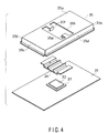
- the flat panel 35a of the shielding case 35 may have a notch 35h provided in a heat sink 34 facing portion thereof so that two tabs extend in the notch 35h.
- the two tabs of the flat panel 35a are bent into an L shape, they serve as the holding panels 35f and 35g. This allows the heat sink 34 to be exposed outwardly through the notch 35h, thus increasing the effect of heat radiation.
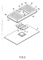
- the flat panel 35a of the shielding case 35 has a plurality of perforations 35i provided therein so long as the shielding effect is not interrupted. Accordingly, the effect of heat radiation will further be improved.
- FIG. 6 illustrates another embodiment of the present invention.
- the same components are denoted by the same numerals as those shown in FIG. 3.
- Holding panels 35f and 35g extending vertically from a flat panel 35a of a shielding case 35 are arranged to remain pressed by and sandwiched between two side panels 34b and 34c of a heat sink 34.
- the heat sink 34 is securely held by the resilient force of the holding panels 35f and 35g.
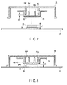
- FIGS. 7 and 8 illustrates a further embodiment of the present invention.
- the same components are denoted by the same numerals as those shown in FIG. 6.
- a shielding case 35 and a heat sink 34 are coupled together with holding panels 35f and 35g of the shielding case 35 pressed against side panels 34b and 34c of the heat sink 34 by their resilient force, there is a clearance d1 between the distal end of each of the holding panels 35f and 35g and board 34a of the heat sink 34.
- the thickness of a heat conductive sheet 33 is d2 (> d1) under a no-load condition.
- the shielding case 35 is lowered from above towards a circuit board 31, the board 34a of the heat sink 34 comes into direct contact with the heat conductive sheet 33.
- the holding panels 35f and 35g of the shielding case 35 slide down along the side panels 34b and 34c of the heat sink 34 and their distal ends come closer to the board 34a of the heat sink 34 to narrow the clearance d1.
- the four side panels 35b to 35e of the shielding case 35 are attached to the circuit board 31 and the thickness of the heat conductive sheet 33 is d3 ( ⁇ d2) as best shown in FIG. 8.
- the heat conductive sheet 33 is thus sandwiched directly between the heat sink 34 and the LSI 32 on the circuit board 31 under pressure.
- heat generated by the LSI 32 can effectively be transferred across the heat conductive sheet 33 to the heat sink 34 and radiated outwardly at a higher efficiency.
- the shielding case 35 and the heat sink 34 remain electrically connected to each other at a favorable stability. Accordingly, the heat sink 34 can act as one part of the shielding case 35 of which the electromagnetic shielding effect will thus be enhanced.
- FIGS. 9 and 10 illustrates a still further embodiment of the present invention.
- the same components are denoted by the same numerals as those shown in FIGS. 7 and 8.
- side panels 34b and 34c of a heat sink 34 have slots 34b2 and 34c2 provided therein
- holding panels 35f and 35g of a shielding case 35 have projections 35f2 and 35g2 provided thereon for loosely fitting into the corresponding slots 34b2 and 34c2.
- the holding panels 35f and 35g of the shielding case 35 in the embodiments shown in FIGS. 6 to 10 are modified to such an arrangement shown in FIG. 4 or the flat panel 35a of the shielding case 35 is modified to have such a plurality of through perforations 35i provided therein as shown in FIG. 5.
- the present invention is not limited to the foregoing embodiments but various changes and modifications of its components may be made without departing from the scope of the present invention.
- the components disclosed in the embodiments may be assembled in any combination for embodying the present invention. For example, some of the components may be omitted from all the components disclosed in the embodiments. Further, components in different embodiments may be appropriately combined.
Landscapes
- Engineering & Computer Science (AREA)
- Microelectronics & Electronic Packaging (AREA)
- Physics & Mathematics (AREA)
- Thermal Sciences (AREA)
- Cooling Or The Like Of Electrical Apparatus (AREA)
- Shielding Devices Or Components To Electric Or Magnetic Fields (AREA)
- Cooling Or The Like Of Semiconductors Or Solid State Devices (AREA)
Applications Claiming Priority (1)
| Application Number | Priority Date | Filing Date | Title |
|---|---|---|---|
| JP2005031953A JP4498163B2 (ja) | 2005-02-08 | 2005-02-08 | 電子機器の放熱装置 |
Publications (1)
| Publication Number | Publication Date |
|---|---|
| EP1689220A2 true EP1689220A2 (de) | 2006-08-09 |
Family
ID=36498973
Family Applications (1)
| Application Number | Title | Priority Date | Filing Date |
|---|---|---|---|
| EP05108116A Withdrawn EP1689220A2 (de) | 2005-02-08 | 2005-09-05 | Wärmeabfuhranordnung und Verfahren in einer elektronischen Vorrichtung |
Country Status (5)
| Country | Link |
|---|---|
| US (1) | US7312998B2 (de) |
| EP (1) | EP1689220A2 (de) |
| JP (1) | JP4498163B2 (de) |
| KR (1) | KR100701000B1 (de) |
| CN (1) | CN100455176C (de) |
Cited By (3)
| Publication number | Priority date | Publication date | Assignee | Title |
|---|---|---|---|---|
| FR2944408A1 (fr) * | 2009-04-14 | 2010-10-15 | Eads Aeronautic Defence And Sp | Boitier pour carte electronique embarquee |
| CN103167786A (zh) * | 2011-12-12 | 2013-06-19 | 洛克威尔自动控制技术股份有限公司 | 负荷被分配的热沉系统 |
| EP2811516A3 (de) * | 2013-06-07 | 2015-04-29 | Hamilton Sundstrand Corporation | Wärmeableitungsvorrichtung |
Families Citing this family (55)
| Publication number | Priority date | Publication date | Assignee | Title |
|---|---|---|---|---|
| JP2006222388A (ja) * | 2005-02-14 | 2006-08-24 | Toshiba Corp | 電子機器の放熱装置及び放熱方法 |
| JP2006229046A (ja) * | 2005-02-18 | 2006-08-31 | Toshiba Corp | 電子機器の放熱装置及び放熱方法 |
| JP4445409B2 (ja) * | 2005-02-23 | 2010-04-07 | 株式会社東芝 | 電子機器の放熱装置 |
| US7524206B2 (en) * | 2005-03-23 | 2009-04-28 | Pulse Engineering, Inc. | Power-enabled connector assembly with heat dissipation apparatus and method of manufacturing |
| WO2008029638A1 (en) * | 2006-09-07 | 2008-03-13 | Kabushiki Kaisha Yaskawa Denki | Motor controller |
| CN101277599A (zh) * | 2007-03-30 | 2008-10-01 | 富准精密工业(深圳)有限公司 | 散热装置 |
| US20090002949A1 (en) * | 2007-06-29 | 2009-01-01 | Lucent Technologies Inc. | Heat transfer for electronic component via an electromagnetic interference (emi) shield having shield deformation |
| JP2009060048A (ja) * | 2007-09-03 | 2009-03-19 | Toshiba Corp | シールドケース装置および表示装置 |
| CN201138907Y (zh) * | 2007-12-29 | 2008-10-22 | 鸿富锦精密工业(深圳)有限公司 | 电子装置壳体 |
| CN101543411B (zh) | 2008-03-24 | 2014-05-28 | 深圳迈瑞生物医疗电子股份有限公司 | 平板伸缩机构 |
| CN101568247B (zh) | 2008-04-25 | 2012-09-05 | 深圳迈瑞生物医疗电子股份有限公司 | 屏蔽绝缘散热系统 |
| JP4473923B2 (ja) * | 2008-10-22 | 2010-06-02 | 株式会社東芝 | 電子機器 |
| CN102026522A (zh) * | 2009-09-17 | 2011-04-20 | 富准精密工业(深圳)有限公司 | 散热模组 |
| USD624510S1 (en) * | 2009-10-30 | 2010-09-28 | SemiLEDs Optoelectronics Co., Ltd. | Light emitting diode device |
| USD618637S1 (en) * | 2009-10-30 | 2010-06-29 | SemiLEDs Optoelectronics Co., Ltd. | Light emitting diode device |
| JP5306263B2 (ja) * | 2010-03-03 | 2013-10-02 | 株式会社東芝 | 電子機器 |
| TW201143585A (en) * | 2010-05-17 | 2011-12-01 | Hon Hai Prec Ind Co Ltd | Electronic device |
| CN102253698A (zh) * | 2010-05-18 | 2011-11-23 | 鸿富锦精密工业(深圳)有限公司 | 电子装置 |
| JP5065443B2 (ja) * | 2010-05-28 | 2012-10-31 | 株式会社藤商事 | 遊技機 |
| JP5899473B2 (ja) | 2011-02-03 | 2016-04-06 | パナソニックIpマネジメント株式会社 | 電子機器の冷却構造 |
| KR101861278B1 (ko) * | 2012-03-22 | 2018-05-25 | 엘지전자 주식회사 | 이동 단말기 |
| KR101994931B1 (ko) | 2012-07-19 | 2019-07-01 | 삼성전자주식회사 | 기억 장치 |
| US20150216074A1 (en) * | 2012-08-02 | 2015-07-30 | Mitsubishi Electric Corporation | Heat dissipation plate |
| JP2014036187A (ja) * | 2012-08-10 | 2014-02-24 | Stanley Electric Co Ltd | 放熱構造及びこの放熱構造が設けられた発熱素子装置 |
| US9265180B2 (en) * | 2012-09-07 | 2016-02-16 | Thomson Licensing | Set top box having heat sink pressure applying means |
| JP2014093414A (ja) * | 2012-11-02 | 2014-05-19 | Hitachi Automotive Systems Ltd | 電子制御装置 |
| EP2736311B1 (de) * | 2012-11-27 | 2017-08-16 | Siemens Aktiengesellschaft | Automatisierungsgerät mit Kühlkörper |
| US9215833B2 (en) * | 2013-03-15 | 2015-12-15 | Apple Inc. | Electronic device with heat dissipating electromagnetic interference shielding structures |
| JP2014187230A (ja) * | 2013-03-25 | 2014-10-02 | Ricoh Co Ltd | 電子機器及び通信装置 |
| KR102148201B1 (ko) * | 2013-05-06 | 2020-08-26 | 삼성전자주식회사 | 제어장치 |
| TW201446120A (zh) * | 2013-05-30 | 2014-12-01 | Wistron Corp | 電子裝置之散熱機構 |
| KR102123245B1 (ko) * | 2013-10-21 | 2020-06-16 | 엘지전자 주식회사 | 노이즈를 차폐하는 방열 부재 및 이를 구비하는 전자 기기 |
| JP6282472B2 (ja) * | 2014-01-30 | 2018-02-21 | Next Innovation合同会社 | 熱伝達機構及び熱伝達体 |
| US9357670B2 (en) * | 2014-02-18 | 2016-05-31 | Lockheed Martin Corporation | Efficient heat transfer from conduction-cooled circuit cards |
| KR102334326B1 (ko) * | 2014-02-24 | 2021-12-02 | 삼성전자주식회사 | 하드웨어 쉴드 장치 및 이를 포함하는 전자 장치 |
| CN104378954A (zh) * | 2014-10-13 | 2015-02-25 | 上海仪电数字技术有限公司 | 电子器件的散热器 |
| DE102015202142A1 (de) * | 2015-02-06 | 2016-08-11 | Mahle International Gmbh | Elektrische Einrichtung |
| JP6036894B2 (ja) * | 2015-03-26 | 2016-11-30 | 日本電気株式会社 | 冷却装置および装置 |
| CN106328612A (zh) * | 2015-06-25 | 2017-01-11 | 浙江盾安人工环境股份有限公司 | 一种芯片散热装置及其电子组件 |
| JP6565456B2 (ja) * | 2015-08-05 | 2019-08-28 | Tdk株式会社 | 電子回路装置および電子回路装置の放熱構造 |
| FR3049160B1 (fr) * | 2016-03-15 | 2018-04-13 | Aptiv Technologies Limited | Dispositif electronique et methode d'assemblage d'un tel dispositif |
| CN106170199B (zh) * | 2016-08-31 | 2023-01-20 | 广东虹勤通讯技术有限公司 | 一种散热屏蔽系统及通信产品 |
| US10390456B2 (en) * | 2016-11-07 | 2019-08-20 | Rockwell Automation Technologies, Inc. | Controller with fan monitoring and control |
| JP6645487B2 (ja) * | 2017-10-30 | 2020-02-14 | セイコーエプソン株式会社 | プリント回路板 |
| US10522990B1 (en) * | 2018-08-29 | 2019-12-31 | The Boeing Company | System and method for an under floor seat-to-seat wiring trough to facilitate flat floors in aircraft passenger cabin |
| KR102656239B1 (ko) * | 2018-11-27 | 2024-04-09 | 엘지디스플레이 주식회사 | 디스플레이 장치 |
| USD924346S1 (en) | 2019-02-01 | 2021-07-06 | Parsons Xtreme Golf, LLC | Golf club head |
| JP2020202036A (ja) * | 2019-06-06 | 2020-12-17 | 株式会社オートネットワーク技術研究所 | シールドコネクタ |
| EP3749072A1 (de) * | 2019-06-07 | 2020-12-09 | ZKW Group GmbH | Verfahren zur herstellung eines ein steuergerät umschliessenden gehäuses |
| JP6905016B2 (ja) * | 2019-09-10 | 2021-07-21 | Necプラットフォームズ株式会社 | 実装基板構造 |
| CN113257759A (zh) * | 2020-02-10 | 2021-08-13 | 华为技术有限公司 | 散热器、单板、电子设备及制造方法 |
| US11505321B2 (en) | 2020-06-15 | 2022-11-22 | The Boeing Company | Underfloor wire routing system for passenger cabin |
| KR102516851B1 (ko) * | 2022-05-11 | 2023-04-03 | (주) 넥스원이노베이션 | 방열기능을 구비한 차폐부재 |
| WO2025135118A1 (ja) * | 2023-12-21 | 2025-06-26 | 本田技研工業株式会社 | 電子機器の筐体構造 |
| KR102798807B1 (ko) * | 2024-04-22 | 2025-04-22 | 한국항공우주연구원 | 단열 또는 전자기파 차폐 블록 모듈 |
Citations (5)
| Publication number | Priority date | Publication date | Assignee | Title |
|---|---|---|---|---|
| US5060114A (en) | 1990-06-06 | 1991-10-22 | Zenith Electronics Corporation | Conformable pad with thermally conductive additive for heat dissipation |
| US5384940A (en) | 1992-02-28 | 1995-01-31 | Aavid Engineering, Inc. | Self-locking heat sinks for surface mount devices |
| JPH0964582A (ja) | 1995-08-21 | 1997-03-07 | Matsushita Electric Ind Co Ltd | シールドケース構造 |
| US6445583B1 (en) | 2001-01-26 | 2002-09-03 | Laird Technologies, Inc. | Snap in heat sink shielding lid |
| JP2002359330A (ja) | 2001-06-01 | 2002-12-13 | Ryosan Co Ltd | ヒートシンク固定具、ヒートシンク、ヒートシンク固定方法 |
Family Cites Families (15)
| Publication number | Priority date | Publication date | Assignee | Title |
|---|---|---|---|---|
| JP3178985B2 (ja) | 1995-03-24 | 2001-06-25 | 株式会社東芝 | 携帯形電子機器 |
| JPH08279689A (ja) * | 1995-04-10 | 1996-10-22 | Matsushita Electric Ind Co Ltd | 半導体素子のシールド装置 |
| JPH10173371A (ja) * | 1996-12-13 | 1998-06-26 | Kokusai Electric Co Ltd | 電子機器の筐体構造 |
| JP3597368B2 (ja) * | 1998-02-16 | 2004-12-08 | アルプス電気株式会社 | 電子機器 |
| JP3619670B2 (ja) * | 1998-05-27 | 2005-02-09 | アルプス電気株式会社 | 電子機器 |
| US6061235A (en) * | 1998-11-18 | 2000-05-09 | Hewlett-Packard Company | Method and apparatus for a modular integrated apparatus for heat dissipation, processor integration, electrical interface, and electromagnetic interference management |
| JP4438164B2 (ja) | 2000-03-01 | 2010-03-24 | ソニー株式会社 | シールドケース |
| JP2001326492A (ja) * | 2000-05-17 | 2001-11-22 | Casio Comput Co Ltd | 熱および電磁ノイズ兼用対策部品、および電子機器 |
| US6545871B1 (en) * | 2000-10-27 | 2003-04-08 | Thomson Licensing, S.A. | Apparatus for providing heat dissipation for a circuit element |
| JP4300706B2 (ja) * | 2000-12-21 | 2009-07-22 | ソニー株式会社 | 電子機器の放熱装置 |
| JP3576512B2 (ja) * | 2001-09-27 | 2004-10-13 | 三菱重工業株式会社 | 電子回路収納ケース、室外ユニット、及び空気調和装置 |
| US6673998B1 (en) * | 2003-01-02 | 2004-01-06 | Accton Technology Corporation | Electromagnetic shielding device with heat-dissipating capability |
| JP4043986B2 (ja) | 2003-03-31 | 2008-02-06 | 古河電気工業株式会社 | 放熱フィンを備えたヒートシンクおよび放熱フィンの固定方法 |
| US7095626B2 (en) * | 2003-05-29 | 2006-08-22 | Interplex Nas Inc. | Openable one-piece electrical RF shield and method of manufacturing the same |
| TWI316387B (en) * | 2003-12-30 | 2009-10-21 | Asustek Comp Inc | Electronic apparatus and shielding module thereof |
-
2005
- 2005-02-08 JP JP2005031953A patent/JP4498163B2/ja not_active Expired - Fee Related
- 2005-09-05 EP EP05108116A patent/EP1689220A2/de not_active Withdrawn
- 2005-09-13 US US11/225,779 patent/US7312998B2/en not_active Expired - Fee Related
- 2005-09-15 KR KR1020050085999A patent/KR100701000B1/ko not_active Expired - Fee Related
- 2005-09-15 CN CNB2005101040721A patent/CN100455176C/zh not_active Expired - Fee Related
Patent Citations (5)
| Publication number | Priority date | Publication date | Assignee | Title |
|---|---|---|---|---|
| US5060114A (en) | 1990-06-06 | 1991-10-22 | Zenith Electronics Corporation | Conformable pad with thermally conductive additive for heat dissipation |
| US5384940A (en) | 1992-02-28 | 1995-01-31 | Aavid Engineering, Inc. | Self-locking heat sinks for surface mount devices |
| JPH0964582A (ja) | 1995-08-21 | 1997-03-07 | Matsushita Electric Ind Co Ltd | シールドケース構造 |
| US6445583B1 (en) | 2001-01-26 | 2002-09-03 | Laird Technologies, Inc. | Snap in heat sink shielding lid |
| JP2002359330A (ja) | 2001-06-01 | 2002-12-13 | Ryosan Co Ltd | ヒートシンク固定具、ヒートシンク、ヒートシンク固定方法 |
Cited By (7)
| Publication number | Priority date | Publication date | Assignee | Title |
|---|---|---|---|---|
| FR2944408A1 (fr) * | 2009-04-14 | 2010-10-15 | Eads Aeronautic Defence And Sp | Boitier pour carte electronique embarquee |
| WO2010118971A1 (fr) * | 2009-04-14 | 2010-10-21 | European Aeronautic Defence And Space Company Eads France | Boîtier pour carte électronique embarquée |
| CN102428765A (zh) * | 2009-04-14 | 2012-04-25 | 欧洲航空防务与空间公司Eads法国 | 用于机载电子卡的壳体 |
| US8947881B2 (en) | 2009-04-14 | 2015-02-03 | European Aeronautic Defence And Space Company Eads France | Housing for an on-board electronic card |
| CN102428765B (zh) * | 2009-04-14 | 2015-05-06 | 欧洲航空防务与空间公司Eads法国 | 用于机载电子卡的壳体 |
| CN103167786A (zh) * | 2011-12-12 | 2013-06-19 | 洛克威尔自动控制技术股份有限公司 | 负荷被分配的热沉系统 |
| EP2811516A3 (de) * | 2013-06-07 | 2015-04-29 | Hamilton Sundstrand Corporation | Wärmeableitungsvorrichtung |
Also Published As
| Publication number | Publication date |
|---|---|
| CN100455176C (zh) | 2009-01-21 |
| KR100701000B1 (ko) | 2007-03-29 |
| JP4498163B2 (ja) | 2010-07-07 |
| US7312998B2 (en) | 2007-12-25 |
| US20060176672A1 (en) | 2006-08-10 |
| CN1819755A (zh) | 2006-08-16 |
| JP2006222146A (ja) | 2006-08-24 |
| KR20060090560A (ko) | 2006-08-14 |
Similar Documents
| Publication | Publication Date | Title |
|---|---|---|
| US7312998B2 (en) | Heat radiating apparatus in electronic device and heat radiating method | |
| JP2006229046A (ja) | 電子機器の放熱装置及び放熱方法 | |
| JP4445409B2 (ja) | 電子機器の放熱装置 | |
| JP2006222388A (ja) | 電子機器の放熱装置及び放熱方法 | |
| US20020186542A1 (en) | Heat sink of module with built-in IC | |
| US20060040562A1 (en) | Connector with built-in substrate and its assembling method | |
| US8928434B2 (en) | Complex tuner module | |
| US6094360A (en) | HF module with housing and printed circuit board arranged therein | |
| JP2009188956A (ja) | チューナモジュールのシールド構造およびそれを備える受信装置 | |
| US8031899B2 (en) | Microphone | |
| US7072174B2 (en) | Television tuner and housing structure for electronic equipment | |
| JP2008198785A (ja) | 高周波ユニット | |
| GB2319397A (en) | A mounting structure for a printed circuit board | |
| JP2007012941A (ja) | 電子機器、およびこの電子機器に組み込まれたヒートシンク | |
| US6580612B2 (en) | Electric circuit | |
| JP2004235738A (ja) | 電子装置及び選局装置 | |
| JP5112145B2 (ja) | 受信装置 | |
| KR100628134B1 (ko) | 영상표시장치의 확장카드 슬롯 어셈블리 | |
| JP2007266207A (ja) | 回路基板およびシールドカバー取付方法 | |
| KR100843439B1 (ko) | 탄성형 방열부 및 이를 갖는 전자 장치 | |
| JP2006310965A (ja) | デジタル放送受信装置 | |
| JP4626457B2 (ja) | ケースとこれを用いた電子機器 | |
| JP2007103610A (ja) | 電子装置 | |
| JP2002026545A (ja) | ガイドレール構造 | |
| JP2007104224A (ja) | チューナユニット |
Legal Events
| Date | Code | Title | Description |
|---|---|---|---|
| PUAI | Public reference made under article 153(3) epc to a published international application that has entered the european phase |
Free format text: ORIGINAL CODE: 0009012 |
|
| 17P | Request for examination filed |
Effective date: 20050906 |
|
| AK | Designated contracting states |
Kind code of ref document: A2 Designated state(s): AT BE BG CH CY CZ DE DK EE ES FI FR GB GR HU IE IS IT LI LT LU LV MC NL PL PT RO SE SI SK TR |
|
| AX | Request for extension of the european patent |
Extension state: AL BA HR MK YU |
|
| STAA | Information on the status of an ep patent application or granted ep patent |
Free format text: STATUS: THE APPLICATION HAS BEEN WITHDRAWN |
|
| 18W | Application withdrawn |
Effective date: 20090303 |