EP1656242B1 - Capillary imprinting technique - Google Patents
Capillary imprinting technique Download PDFInfo
- Publication number
- EP1656242B1 EP1656242B1 EP04781082A EP04781082A EP1656242B1 EP 1656242 B1 EP1656242 B1 EP 1656242B1 EP 04781082 A EP04781082 A EP 04781082A EP 04781082 A EP04781082 A EP 04781082A EP 1656242 B1 EP1656242 B1 EP 1656242B1
- Authority
- EP
- European Patent Office
- Prior art keywords
- mold
- conformable material
- substrate
- region
- sub
- Prior art date
- Legal status (The legal status is an assumption and is not a legal conclusion. Google has not performed a legal analysis and makes no representation as to the accuracy of the status listed.)
- Expired - Lifetime
Links
Images


Classifications
-
- B—PERFORMING OPERATIONS; TRANSPORTING
- B29—WORKING OF PLASTICS; WORKING OF SUBSTANCES IN A PLASTIC STATE IN GENERAL
- B29C—SHAPING OR JOINING OF PLASTICS; SHAPING OF MATERIAL IN A PLASTIC STATE, NOT OTHERWISE PROVIDED FOR; AFTER-TREATMENT OF THE SHAPED PRODUCTS, e.g. REPAIRING
- B29C59/00—Surface shaping of articles, e.g. embossing; Apparatus therefor
- B29C59/02—Surface shaping of articles, e.g. embossing; Apparatus therefor by mechanical means, e.g. pressing
-
- G—PHYSICS
- G03—PHOTOGRAPHY; CINEMATOGRAPHY; ANALOGOUS TECHNIQUES USING WAVES OTHER THAN OPTICAL WAVES; ELECTROGRAPHY; HOLOGRAPHY
- G03F—PHOTOMECHANICAL PRODUCTION OF TEXTURED OR PATTERNED SURFACES, e.g. FOR PRINTING, FOR PROCESSING OF SEMICONDUCTOR DEVICES; MATERIALS THEREFOR; ORIGINALS THEREFOR; APPARATUS SPECIALLY ADAPTED THEREFOR
- G03F7/00—Photomechanical, e.g. photolithographic, production of textured or patterned surfaces, e.g. printing surfaces; Materials therefor, e.g. comprising photoresists; Apparatus specially adapted therefor
- G03F7/0002—Lithographic processes using patterning methods other than those involving the exposure to radiation, e.g. by stamping
-
- B—PERFORMING OPERATIONS; TRANSPORTING
- B29—WORKING OF PLASTICS; WORKING OF SUBSTANCES IN A PLASTIC STATE IN GENERAL
- B29C—SHAPING OR JOINING OF PLASTICS; SHAPING OF MATERIAL IN A PLASTIC STATE, NOT OTHERWISE PROVIDED FOR; AFTER-TREATMENT OF THE SHAPED PRODUCTS, e.g. REPAIRING
- B29C35/00—Heating, cooling or curing, e.g. crosslinking or vulcanising; Apparatus therefor
- B29C35/02—Heating or curing, e.g. crosslinking or vulcanizing during moulding, e.g. in a mould
- B29C35/08—Heating or curing, e.g. crosslinking or vulcanizing during moulding, e.g. in a mould by wave energy or particle radiation
-
- B—PERFORMING OPERATIONS; TRANSPORTING
- B82—NANOTECHNOLOGY
- B82Y—SPECIFIC USES OR APPLICATIONS OF NANOSTRUCTURES; MEASUREMENT OR ANALYSIS OF NANOSTRUCTURES; MANUFACTURE OR TREATMENT OF NANOSTRUCTURES
- B82Y10/00—Nanotechnology for information processing, storage or transmission, e.g. quantum computing or single electron logic
-
- B—PERFORMING OPERATIONS; TRANSPORTING
- B82—NANOTECHNOLOGY
- B82Y—SPECIFIC USES OR APPLICATIONS OF NANOSTRUCTURES; MEASUREMENT OR ANALYSIS OF NANOSTRUCTURES; MANUFACTURE OR TREATMENT OF NANOSTRUCTURES
- B82Y40/00—Manufacture or treatment of nanostructures
-
- C—CHEMISTRY; METALLURGY
- C23—COATING METALLIC MATERIAL; COATING MATERIAL WITH METALLIC MATERIAL; CHEMICAL SURFACE TREATMENT; DIFFUSION TREATMENT OF METALLIC MATERIAL; COATING BY VACUUM EVAPORATION, BY SPUTTERING, BY ION IMPLANTATION OR BY CHEMICAL VAPOUR DEPOSITION, IN GENERAL; INHIBITING CORROSION OF METALLIC MATERIAL OR INCRUSTATION IN GENERAL
- C23F—NON-MECHANICAL REMOVAL OF METALLIC MATERIAL FROM SURFACE; INHIBITING CORROSION OF METALLIC MATERIAL OR INCRUSTATION IN GENERAL; MULTI-STEP PROCESSES FOR SURFACE TREATMENT OF METALLIC MATERIAL INVOLVING AT LEAST ONE PROCESS PROVIDED FOR IN CLASS C23 AND AT LEAST ONE PROCESS COVERED BY SUBCLASS C21D OR C22F OR CLASS C25
- C23F1/00—Etching metallic material by chemical means
- C23F1/08—Apparatus, e.g. for photomechanical printing surfaces
Definitions
- the field of invention relates generally to micro-fabrication of structures. More particularly, the present invention is directed to patterning substrates in furtherance of the formation of structures.
- Micro-fabrication involves the fabrication of very small structures, e.g., having features on the order of micro-meters or smaller.
- One area in which micro-fabrication has had a sizeable impact is in the processing of integrated circuits.
- micro-fabrication becomes increasingly important.
- Micro-fabrication provides greater process control while allowing a reduction in the minimum feature dimension of the structures formed.
- Other areas of development in which micro-fabrication has been employed include biotechnology, optical technology, mechanical systems and the like.
- Willson et al. discloses a method of forming a relief image in a substrate.
- the method includes having a mold make mechanical contact with the polymerizable fluid disposed on a substrate.
- the mold includes a relief structure. Under the compressive force created between the mold and substrate, the polymerizable fluid fills the relief structure in the mold. Thereafter, the polymerizable fluid is subjected to conditions to solidify and polymerize the same, forming a solidified polymeric material on a transfer layer that contains a relief structure complimentary.to that of the relief structure of the mold.
- the mold is then separated from the solid polymeric material such that a replica of the relief structure in the mold is formed in the solidified polymeric material. Post processing steps are undertaken to transfer the relief image into the substrate.
- the present invention provides a method for patterning a substrate with a template having a mold according to claim 1. Specifically, the movement between the mold and the substrate is controlled to a sufficient degree to attenuate, if not avoid, compressive forces between the mold and the substrate. As a result, upon initial contact of the mold with the conformable material, spontaneous capillary filling of the volume between the mold and the substrate occurs. The capillary filling creates pulling forces between the mold and the substrate, which is referred to as a negative imprint force. Many benefits result from the negative imprint force, including rapid and complete filling of the features of the mold, as well as precise control of the distribution of the conformable material of the substrate. These and other embodiments are described more fully below.
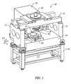
- Fig. 1 is a perspective view of a patterning system in accordance with the present invention
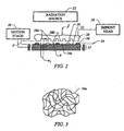
- Fig. 2 is a simplified elevation view of a patterning system shown in Fig. 1 ;
- Fig. 3 is a simplified representation of material from which an imprinting layer, shown in Fig. 2 , is comprised before being polymerized and cross-linked;
- Fig. 4 is a simplified representation of cross-linked polymer material into which the material shown in Fig. 3 is transformed after being subjected to radiation;
- Fig. 5 is a simplified elevation view of a mold spaced-apart from the imprinting layer, shown in Fig. 2 , after patterning of the imprinting layer;
- Fig. 6 is a graphical representation of the forces to which a mold, shown in Fig. 2 , is subjected during imprinting processes, in accordance with one embodiment of the present invention
- Fig. 7 is a detailed view of the system shown in Fig. 1 ;
- Fig. 8 is a graphical representation of the forces to which a mold, shown in Fig. 2 , is subjected during imprinting processes in accordance with an alternate embodiment of the present invention
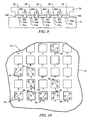
- Fig. 9 is a close-up view of the template, shown in Fig. 1 , having multiple molds formed thereon to concurrently imprint multiple pattern regions on the substrate in accordance with the present invention
- Fig. 10 is a top down plan view of a portion of the substrate, shown in Fig. 1 , showing a plurality of regions that are in superimposition with the molds of template, shown in Fig. 9 , in accordance with the present invention;
- Fig. 11 is a detailed side view showing a portion of the mold, shown in Fig. 2 , extending from an edge of the substrate, in accordance with an alternate embodiment of the present invention.
- Fig. 12 is a simplified elevation view of material in an imprint device and substrate employed with the present invention in accordance with an alternate embodiment.
- Fig. 1 depicts a lithographic system 10 in accordance with one embodiment of the present invention that includes a pair of spaced-apart bridge supports 12 having a bridge 14 and a stage support 16 extending therebetween. Bridge 14 and stage support 16 are spaced-apart. Coupled to bridge 14 is an imprint head 18, which extends from bridge 14 toward stage support 16. Disposed upon stage support 16 to face imprint head 18 is a motion stage 20. Motion stage 20 is configured to move with respect to stage support 16 along X and Y axes, and may optionally facilitate movement along a Z axis, as well.
- a radiation source 22 is coupled to lithographic system 10 to impinge actinic radiation upon motion stage 20. As shown, radiation source 22 is coupled to bridge 14 and includes a power generator 23 connected to radiation source 22.
- Mold 28 includes a plurality of features defined by a plurality of spaced-apart recessions 28a and protrusions 28b.
- the plurality of features defines an original pattern that is to be transferred into a substrate 31 positioned on motion stage 20.
- Substrate 31 may comprise of a bare wafer or a wafer with one or more layers disposed thereon.
- imprint head 18 is adapted to move along the Z axis and vary a distance "d" between mold 28 and substrate 31. In this manner, the features on mold 28 may be imprinted into a conformable region of substrate 31, discussed more fully below.
- Radiation source 22 is located so that mold 28 is positioned between radiation source 22 and substrate 31.
- mold 28 is fabricated from material that allows it to be substantially transparent to the radiation produced by radiation source 22.
- a conformable region such as an imprinting layer 34, is disposed on a portion of surface 32 that presents a substantially planar profile.
- the conformable region may be formed using any known technique to produce conformable material, such as a hot embossing process disclosed in United States patent number 5,772,905 to Chou , or a laser assisted direct imprinting (LADI) process of the type described by Chou et al. in Ultrafast and Direct Imprint of Nanostructures in Silicon, Nature, Col. 417, pp. 835-837, June 2002 .
- LADI laser assisted direct imprinting
- conformable region consists of imprinting layer 34 being deposited as a plurality of spaced-apart discrete droplets 36 of imprinting material 36a on substrate 31, discussed more fully below.
- Imprinting layer 34 is formed from imprinting material 36a that may be selectively polymerized and cross-linked to record a pattern that is complementary to the original pattern, defining a recorded pattern.
- Imprinting material 36a is shown in Fig. 4 as being cross-linked at points 36b, forming cross-linked polymer material 36c.
- radiation source 22 produces actinic radiation that polymerizes and cross-links imprinting material 36a, forming polymer material 36c in which a substantial portion thereof is cross-linked.
- imprinting material 36a transforms to polymer material 36c, which is a solid, forming imprinting layer 134, shown in Fig. 5 .
- polymer material 36c is solidified to provide side 34c of imprinting layer 134 with a shape conforming to a shape of a surface 28c of mold 28, with imprinting layer 134 having recesses 30.
- imprint head 18, shown in Fig. 2 is moved to increase distance "d” so that mold 28 and imprinting layer 134 are spaced-apart.
- the pattern recorded in imprinting layer 34 may be produced primarily, if not solely, by capillary force of imprinting material 36a with mold 28 and/or substrate 31.
- the amount of external force, i.e., non-capillary pressure, employed is dependent upon several factors, including the composition of imprinting material 36a, the resulting thickness of imprinting layer 34 and the area over which imprinting material 36a must spread.
- a fixed composition of imprinting material 36a and a fixed area over which imprinting material 36a is to spread there is a minimum distance d' between substrate 31 and protrusions 28b that is reached before capillary filling occurs.
- imprinting layer 34 greater than d' very little capillary pressure would be employed to spread imprinting material 36a, i.e., a greater amount of compressive forces would be exerted on mold 28.
- an external positive force F is employed to spread imprinting material 36a in droplets 36 in a desirable amount of time.
- imprinting material 36a in droplets 36 is spread primarily with external pressure applied thereto via mold 28 a sufficient amount until imprinting material 36a is spread between mold 28 and substrate 31, as desired.
- the amount of capillary pressure becomes primarily a function of thickness t 2 and the fraction of the fixed area to be filled with imprinting material 36a, i.e., the portion of the fixed area upon which imprinting material 36a is absent. More particularly, the amount of capillary pressure generated during imprinting is proportional to the fraction of the fixed area to be filled and inversely proportional to thickness t 2 . Understanding that thickness t 2 is dependent upon distance d, it becomes important to carefully control distance d during the imprinting process. Control of distance d may be frustrated by compliance in imprint head 18 and/ or motion stage 20.
- force measurements on mold 28 during an exemplary capillary imprint method is shown with point 80 wherein droplets 36 are initially in contact with mold. As shown, the compressive and tensile forces to which mold 28 is subjected are substantially zero. At point 82, capillary filling of volume V is initiated so that mold 28 is subjected to tension force T. At point 84, tension force T has reached a maximum magnitude, i.e., substantially all of imprinting material 36a in volume V is undergoing capillary attraction with mold 28 and substrate 31.
- relative movement of mold 28 and substrate 31 is effectuated to attenuate, if not avoid, subjecting mold 28 to compressive forces resulting from contact with imprinting material 36a.
- the compressive forces C 1 and C 2 shown in Fig. 7 , that are sought to be minimized result from imprint head 18 pushing against mold 28 as imprinting material 36a pushes against mold 28 during imprinting.
- This facilitates spontaneous capillary filling of volume V occurring upon initial contact of mold 28 with imprinting material 36a in droplets 36.
- the capillary filling creates pulling/tensional forces, T, upon mold 28, referred to as a negative imprint force.
- the negative imprinting force, or tension force, T causes elongation of imprint head 18 and substrate 31 subjecting mold 28 to tension force T.
- imprint head 18 would apply pulling force L 1 to attenuate, if not nullify, compressive forces C 1 and C 2 .
- motion stage 20 would generate pulling force L 2 to attenuate, if not nullify, compressive forces C 1 and C 2 or imprint head 18 and motion stage 20 could move in conjunction with one another to attenuate or nullify forces C 1 and C 2 .
- imprint head 18 could apply pushing force S 1 to attenuate, if not nullify, tension force T and/or motion stage 20 would generate pulling force L 2 to attenuate, if not nullify, tension force T.
- the magnitude of tensile and/or compressive forces may be controlled as desired in order to maximize imprinting layer 134 thickness uniformity while still obtaining a desired distance d.
- Figs. 2, 3 and 8 force measurements on mold 28 during an exemplary capillary imprint method employed to maximize thickness uniformity is shown with point 88 wherein droplets 36 are initially in contact with mold. As shown, the compressive and tensile forces to which mold 28 is subjected are substantially zero. At point 90, capillary filling of volume V is initiated so that mold 28 is subjected to tension force T. A point 92, tension force T has reached a maximum magnitude. At point 94, substantially all of imprinting material 36a in volume V has undergone capillary attraction with mold 28, i.e. volume V is substantially filled with imprinting material 36a.
- region 96 either pulling force L 1 or pulling force L 2 or a combination thereof is applied to mold 28, thereby reducing the forces to which the same is subjected to substantially zero at point 96a.
- mold 28 may be subjected to compressive force C 2 that is shown as region 98.
- template 26 may be provided with a plurality of molds 28 so that multiple discrete patterns may be formed on substrate 31, concurrently. Relying on capillary attraction between imprinting material 36a and/or mold 28 and substrate 31, imprinting material 36a does not extend between adjacent patterned areas 31a on substrate 31. Rather, imprinting material 36a remains confined within a region of substrate 31 that is in superimposition with one of the molds 28. As seen, imprinting material 36a forms a meniscus 34d at the periphery of mold 28 due to the surface tension of imprinting material 36a. A hiatus 34c is present between adjacent patterned areas 31a. The surface tension associated with imprinting material 36a in meniscus 34d substantially reduces the probability that imprinting material 36a will extend through hiatus 34c.
- template 26 includes multiple molds 28 in superimposition with a plurality of regions, shown as a-y on substrate 31. It is not necessary to create patterned areas 31a in each of the plurality of regions a-y. Rather, a sub-portion of regions a-y may be provided with droplets 36 of imprinting material 36a, shown as d, k, l, q, s and u-y.
- imprinting material 36a is provided with the requisite properties to completely fill recessions 28a while covering surface 32 with a contiguous formation of imprinting material 36a.
- sub-portions 34b, shown in Fig. 5 of imprinting layer 34 in superimposition with protrusions 28b remain after the desired distance, "d", has been reached, leaving sub-portions 34a with thickness t 1 , and sub-portions 34b with thickness, t 2 .
- Thicknesses "t 1 " and "t 2 " may be any thickness desired, dependent upon the application.
- t 1 is selected so as to be no greater than twice the width u of sub-portions 34a, i.e., t 1 ⁇ 2u, shown more clearly in Fig. 5 .
- substrate 31 and imprinting layer 134 may be etched to transfer the pattern of imprinting layer 134 into substrate 31, providing a patterned surface (not shown).
- the material from which imprinting layer 134 is formed may be varied to define a relative etch rate with respect to substrate 31, as desired.
- imprinting layer 134 may be provided with an etch differential with respect to photo-resist material (not shown) selectively disposed thereon.
- the photo-resist material (not shown) may be provided to further pattern imprinting layer 134, using known techniques. Any etch process may be employed, dependent upon the etch rate desired and the underlying constituents that form substrate 31 and imprinting layer 134. Exemplary etch processes may include plasma etching, reactive ion etching, chemical wet etching and the like.
- an exemplary radiation source 22 may produce ultraviolet radiation; however, any known radiation source may be employed.
- the selection of radiation employed to initiate the polymerization of the material in imprinting layer 34 is known to one skilled in the art and typically depends on the specific application which is desired.
- the plurality of features on mold 28 are shown as recessions 28a extending along a direction parallel to protrusions 28b that provide a cross-section of mold 28 with a shape of a battlement.
- recessions 28a and protrusions 28b may correspond to virtually any feature required to create an integrated circuit and may be as small as a few tens of nanometers.
- the pattern produced by the present patterning technique may be transferred into substrate 31 to provide features having aspect ratios as great as 30:1.
- one embodiment of mold 28 has recessions 28a defining an aspect ratio in a range of 1:1 to 10:1.
- protrusions 28b have a width W 1 in a range of about 10 nm to about 5000 ⁇ m
- recessions 28a have a width W 2 in a range of 10 nm to about 5000 ⁇ m.
- mold 28 and/or template 26 may be formed from various conventional materials, such as, but not limited to, fused-silica, quartz, silicon, organic polymers, siloxane polymers, borosilicate glass, fluorocarbon polymers, metal, hardened sapphire and the like.
- imprinting material 36a is important to efficiently pattern substrate 31 in light of the unique deposition process employed.
- imprinting material 36a is deposited on substrate 31 as a plurality of discrete and spaced-apart droplets 36.
- the combined volume of droplets 36 is such that imprinting material 36a is distributed appropriately over an area of surface 32 where imprinting layer 34 is to be formed.
- imprinting layer 34 is spread and patterned concurrently, with the pattern being subsequently set into imprinting layer 34 by exposure to radiation, such as ultraviolet radiation.
- imprinting material 36a have certain characteristics to facilitate rapid and even spreading of imprinting material 36a in droplets 36 over surface 32 so that all thicknesses t 1 are substantially uniform and all thicknesses t 2 are substantially uniform.
- the desirable characteristics include having a low viscosity, e.g., in a range of 0.5 to 5 centepoise (csp), as well as the ability to wet surface of substrate 31 and/or mold 28 and to avoid subsequent pit or hole formation after polymerization. With these characteristics satisfied, imprinting layer 34 may be made sufficiently thin while avoiding formation of pits or holes in the thinner regions, such as sub-portions 34b, shown in Fig. 5 .
- substrate 31 may be formed from a number of different materials.
- the chemical composition of surface 32 varies dependent upon the material from which substrate 31 is formed.
- substrate 31 may be formed from silicon, plastics, gallium arsenide, mercury telluride, and composites thereof.
- substrate 31 may include one or more layers in sub-portion 34b, e.g., dielectric layer, metal layer, semiconductor layer, planarization layer and the like.
- an exemplary composition for imprinting material 36a is as follows:
- planarization layer 37 may be implemented on substrate 31 that includes a planarization layer 37, shown in Fig. 12 .
- the primary function of planarization layer 37 is to ensure that the surface of substrate 31 is smooth, if not, planar.
- planarization layer 37 may be formed from a number of differing materials, such as, for example, thermoset polymers, thermoplastic polymers, polyepoxies, polyamides, polyurethanes, polycarbonates, polyesters, and combinations thereof.
- Planarization layer 37 is fabricated in such a manner so as to possess a continuous, smooth, relatively defect-free surface that may exhibit excellent adhesion to imprinting layer 34.
- the surface of mold 28 may be treated with a modifying agent.
- imprinting layer 34 is located between planarization layer 37 and the modifying agent.
- a modifying agent is a release layer 39, shown in Fig. 12 .
- Release layer 39 and other surface modifying agents may be applied using any known process.
- processing techniques may include chemical vapor deposition, physical vapor deposition, atomic layer deposition or various other techniques, brazing and the like.
- Exemplary release layers are found in United States application number 10/375,817 , entitled, Method to Reduce Adhesion Between a Polymerizable Layer and a Substrate Employing a Fluorine-Containing Layer , as well as United States application number 10/375,832 , entitled Composition and Method to Form a Release Layer , both of which are assigned to assignee of the present invention.
Landscapes
- Engineering & Computer Science (AREA)
- Chemical & Material Sciences (AREA)
- Nanotechnology (AREA)
- Physics & Mathematics (AREA)
- Crystallography & Structural Chemistry (AREA)
- General Physics & Mathematics (AREA)
- Mechanical Engineering (AREA)
- Metallurgy (AREA)
- Health & Medical Sciences (AREA)
- Chemical Kinetics & Catalysis (AREA)
- General Chemical & Material Sciences (AREA)
- Materials Engineering (AREA)
- Mathematical Physics (AREA)
- Organic Chemistry (AREA)
- Condensed Matter Physics & Semiconductors (AREA)
- Manufacturing & Machinery (AREA)
- Theoretical Computer Science (AREA)
- Toxicology (AREA)
- Oral & Maxillofacial Surgery (AREA)
- Thermal Sciences (AREA)
- Shaping Of Tube Ends By Bending Or Straightening (AREA)
- Moulds For Moulding Plastics Or The Like (AREA)
- Micromachines (AREA)
- Casting Or Compression Moulding Of Plastics Or The Like (AREA)
- Printing Methods (AREA)
- Crystals, And After-Treatments Of Crystals (AREA)
Applications Claiming Priority (2)
| Application Number | Priority Date | Filing Date | Title |
|---|---|---|---|
| US10/645,306 US7442336B2 (en) | 2003-08-21 | 2003-08-21 | Capillary imprinting technique |
| PCT/US2004/026337 WO2005021156A2 (en) | 2003-08-21 | 2004-08-13 | Capillary imprinting technique |
Publications (3)
| Publication Number | Publication Date |
|---|---|
| EP1656242A2 EP1656242A2 (en) | 2006-05-17 |
| EP1656242A4 EP1656242A4 (en) | 2008-01-02 |
| EP1656242B1 true EP1656242B1 (en) | 2011-10-19 |
Family
ID=34273282
Family Applications (1)
| Application Number | Title | Priority Date | Filing Date |
|---|---|---|---|
| EP04781082A Expired - Lifetime EP1656242B1 (en) | 2003-08-21 | 2004-08-13 | Capillary imprinting technique |
Country Status (9)
Families Citing this family (57)
| Publication number | Priority date | Publication date | Assignee | Title |
|---|---|---|---|---|
| EP1303793B1 (en) * | 2000-07-17 | 2015-01-28 | Board Of Regents, The University Of Texas System | Method and system of automatic fluid dispensing for imprint lithography processes |
| US20060005657A1 (en) * | 2004-06-01 | 2006-01-12 | Molecular Imprints, Inc. | Method and system to control movement of a body for nano-scale manufacturing |
| US7077992B2 (en) * | 2002-07-11 | 2006-07-18 | Molecular Imprints, Inc. | Step and repeat imprint lithography processes |
| US7442336B2 (en) * | 2003-08-21 | 2008-10-28 | Molecular Imprints, Inc. | Capillary imprinting technique |
| US7019819B2 (en) | 2002-11-13 | 2006-03-28 | Molecular Imprints, Inc. | Chucking system for modulating shapes of substrates |
| US7641840B2 (en) * | 2002-11-13 | 2010-01-05 | Molecular Imprints, Inc. | Method for expelling gas positioned between a substrate and a mold |
| WO2005030822A2 (en) | 2003-09-23 | 2005-04-07 | University Of North Carolina At Chapel Hill | Photocurable perfluoropolyethers for use as novel materials in microfluidic devices |
| US8211214B2 (en) * | 2003-10-02 | 2012-07-03 | Molecular Imprints, Inc. | Single phase fluid imprint lithography method |
| EP1542074A1 (en) * | 2003-12-11 | 2005-06-15 | Heptagon OY | Manufacturing a replication tool, sub-master or replica |
| CA2549341C (en) | 2003-12-19 | 2014-06-10 | The University Of North Carolina At Chapel Hill | Methods for fabricating isolated micro- and nano- structures using soft or imprint lithography |
| US9040090B2 (en) | 2003-12-19 | 2015-05-26 | The University Of North Carolina At Chapel Hill | Isolated and fixed micro and nano structures and methods thereof |
| SG150506A1 (en) * | 2004-02-13 | 2009-03-30 | Univ North Carolina State | Functional materials and novel methods for the fabrication of microfluidic devices |
| US20060062922A1 (en) | 2004-09-23 | 2006-03-23 | Molecular Imprints, Inc. | Polymerization technique to attenuate oxygen inhibition of solidification of liquids and composition therefor |
| EP1853967A4 (en) * | 2005-02-03 | 2009-11-11 | Univ North Carolina | Low surface area polymer material for use in liquid crystal displays |
| WO2007133235A2 (en) * | 2005-08-08 | 2007-11-22 | Liquidia Technologies, Inc. | Micro and nano-structure metrology |
| EP2537657A3 (en) | 2005-08-09 | 2016-05-04 | The University of North Carolina At Chapel Hill | Methods and materials for fabricating microfluidic devices |
| US8142703B2 (en) * | 2005-10-05 | 2012-03-27 | Molecular Imprints, Inc. | Imprint lithography method |
| JP4533358B2 (ja) * | 2005-10-18 | 2010-09-01 | キヤノン株式会社 | インプリント方法、インプリント装置およびチップの製造方法 |
| US7906058B2 (en) * | 2005-12-01 | 2011-03-15 | Molecular Imprints, Inc. | Bifurcated contact printing technique |
| US7670529B2 (en) * | 2005-12-08 | 2010-03-02 | Molecular Imprints, Inc. | Method and system for double-sided patterning of substrates |
| US7670530B2 (en) * | 2006-01-20 | 2010-03-02 | Molecular Imprints, Inc. | Patterning substrates employing multiple chucks |
| US7943080B2 (en) * | 2005-12-23 | 2011-05-17 | Asml Netherlands B.V. | Alignment for imprint lithography |
| US7459669B2 (en) * | 2005-12-30 | 2008-12-02 | Asml Netherlands B.V. | Sensor and lithographic apparatus |
| US8012395B2 (en) * | 2006-04-18 | 2011-09-06 | Molecular Imprints, Inc. | Template having alignment marks formed of contrast material |
| JP4814682B2 (ja) * | 2006-04-18 | 2011-11-16 | 株式会社日立ハイテクノロジーズ | 微細構造パターンの転写方法及び転写装置 |
| US8215946B2 (en) | 2006-05-18 | 2012-07-10 | Molecular Imprints, Inc. | Imprint lithography system and method |
| US20080181958A1 (en) * | 2006-06-19 | 2008-07-31 | Rothrock Ginger D | Nanoparticle fabrication methods, systems, and materials |
| CN100444027C (zh) * | 2006-07-07 | 2008-12-17 | 中国科学院长春应用化学研究所 | 互补结构微图案化制作倒梯形结构的方法 |
| JP2010503993A (ja) | 2006-09-19 | 2010-02-04 | モレキュラー・インプリンツ・インコーポレーテッド | リフトオフ・パターニング向けの向上したエッチング技法 |
| US20080303187A1 (en) * | 2006-12-29 | 2008-12-11 | Molecular Imprints, Inc. | Imprint Fluid Control |
| WO2008118861A2 (en) * | 2007-03-23 | 2008-10-02 | The University Of North Carolina At Chapel Hill | Discrete size and shape specific organic nanoparticles designed to elicit an immune response |
| US8142702B2 (en) * | 2007-06-18 | 2012-03-27 | Molecular Imprints, Inc. | Solvent-assisted layer formation for imprint lithography |
| US20090014917A1 (en) * | 2007-07-10 | 2009-01-15 | Molecular Imprints, Inc. | Drop Pattern Generation for Imprint Lithography |
| US8119052B2 (en) * | 2007-11-02 | 2012-02-21 | Molecular Imprints, Inc. | Drop pattern generation for imprint lithography |
| US8945444B2 (en) * | 2007-12-04 | 2015-02-03 | Canon Nanotechnologies, Inc. | High throughput imprint based on contact line motion tracking control |
| US20090148619A1 (en) * | 2007-12-05 | 2009-06-11 | Molecular Imprints, Inc. | Controlling Thickness of Residual Layer |
| US8361371B2 (en) * | 2008-02-08 | 2013-01-29 | Molecular Imprints, Inc. | Extrusion reduction in imprint lithography |
| US8187515B2 (en) * | 2008-04-01 | 2012-05-29 | Molecular Imprints, Inc. | Large area roll-to-roll imprint lithography |
| US20100096764A1 (en) * | 2008-10-20 | 2010-04-22 | Molecular Imprints, Inc. | Gas Environment for Imprint Lithography |
| US8586126B2 (en) | 2008-10-21 | 2013-11-19 | Molecular Imprints, Inc. | Robust optimization to generate drop patterns in imprint lithography which are tolerant of variations in drop volume and drop placement |
| US8512797B2 (en) * | 2008-10-21 | 2013-08-20 | Molecular Imprints, Inc. | Drop pattern generation with edge weighting |
| US8652393B2 (en) * | 2008-10-24 | 2014-02-18 | Molecular Imprints, Inc. | Strain and kinetics control during separation phase of imprint process |
| US20100112220A1 (en) * | 2008-11-03 | 2010-05-06 | Molecular Imprints, Inc. | Dispense system set-up and characterization |
| US8464838B2 (en) * | 2009-01-26 | 2013-06-18 | Kenneth C. Brooks | System and method for generating mechanical movement |
| US20100187834A1 (en) * | 2009-01-27 | 2010-07-29 | Brooks Kenneth C | System and method for generating electrical energy |
| NL2003875A (en) * | 2009-02-04 | 2010-08-05 | Asml Netherlands Bv | Imprint lithography method and apparatus. |
| US8715515B2 (en) * | 2009-03-23 | 2014-05-06 | Intevac, Inc. | Process for optimization of island to trench ratio in patterned media |
| US20110030770A1 (en) | 2009-08-04 | 2011-02-10 | Molecular Imprints, Inc. | Nanostructured organic solar cells |
| US20110084417A1 (en) | 2009-10-08 | 2011-04-14 | Molecular Imprints, Inc. | Large area linear array nanoimprinting |
| JP5520270B2 (ja) * | 2011-09-30 | 2014-06-11 | 富士フイルム株式会社 | ナノインプリント用のモールドおよびその製造方法並びにそのモールドを用いたナノインプリント方法およびパターン化基板の製造方法 |
| JP2015088667A (ja) * | 2013-10-31 | 2015-05-07 | 株式会社東芝 | 微細加工システム、微細加工装置、および微細加工方法 |
| WO2016048053A1 (ko) * | 2014-09-26 | 2016-03-31 | 한국기계연구원 | 복수의 나노갭이 형성된 기판 및 이의 제조방법 |
| CN107407868B (zh) * | 2014-11-03 | 2021-08-03 | 武汉大学 | 一种用于毛细纳米印刷的装置和使用该装置进行毛细纳米印刷的方法及其应用 |
| EP3366456A4 (en) * | 2015-10-22 | 2019-05-29 | National Institute of Advanced Industrial Science and Technology | SURFACE STRUCTURE FOR PRINTING BASE MATERIAL AND METHOD FOR THE PRODUCTION THEREOF |
| JP2017152673A (ja) * | 2015-11-05 | 2017-08-31 | ボード・オブ・リージェンツ, ジ・ユニバーシティー・オブ・テキサス・システム | ジェット・アンド・フラッシュ・インプリントリソグラフィにおけるマルチフィールドオーバーレイ制御 |
| US11294277B2 (en) * | 2018-07-25 | 2022-04-05 | Canon Kabushiki Kaisha | Process of imprinting a substrate with fluid control features |
| EP4176311B1 (de) | 2020-07-06 | 2024-05-01 | EV Group E. Thallner GmbH | Verfahren zum erzeugen von mikro- und/oder nanostrukturen |
Family Cites Families (150)
| Publication number | Priority date | Publication date | Assignee | Title |
|---|---|---|---|---|
| US588650A (en) * | 1897-08-24 | Island | ||
| DE2800476A1 (de) | 1977-01-07 | 1978-07-13 | Instruments Sa | Verfahren zur duplizierung einer optischen flaeche sowie so hergestelltes beugungsgitter |
| JPS6053675B2 (ja) | 1978-09-20 | 1985-11-27 | 富士写真フイルム株式会社 | スピンコ−テイング方法 |
| US4512848A (en) | 1984-02-06 | 1985-04-23 | Exxon Research And Engineering Co. | Procedure for fabrication of microstructures over large areas using physical replication |
| DE3614191A1 (de) | 1985-06-27 | 1987-01-08 | Man Technologie Gmbh | Verfahren zur bildung einer oberflaeche hoher guete auf einem bauteil |
| WO1987002935A1 (en) | 1985-11-18 | 1987-05-21 | Eastman Kodak Company | Process for making optical recording media |
| DE3622540A1 (de) * | 1986-07-04 | 1988-01-07 | Bayer Ag | Verfahren zur herstellung von spannungsarmen formteilen |
| FR2604553A1 (fr) | 1986-09-29 | 1988-04-01 | Rhone Poulenc Chimie | Substrat polymere rigide pour disque optique et les disques optiques obtenus a partir dudit substrat |
| US4731155A (en) | 1987-04-15 | 1988-03-15 | General Electric Company | Process for forming a lithographic mask |
| US5132069A (en) | 1987-07-10 | 1992-07-21 | Newton John R | Method of injection molding composite articles |
| US5028366A (en) | 1988-01-12 | 1991-07-02 | Air Products And Chemicals, Inc. | Water based mold release compositions for making molded polyurethane foam |
| JPH01196749A (ja) | 1988-01-30 | 1989-08-08 | Hoya Corp | 光情報記録媒体用基板の製造方法 |
| JPH0224848A (ja) | 1988-07-14 | 1990-01-26 | Canon Inc | 光記録媒体用基板の製造方法 |
| JPH0292603A (ja) | 1988-09-30 | 1990-04-03 | Hoya Corp | 案内溝付き情報記録用基板の製造方法 |
| JPH02192045A (ja) | 1989-01-20 | 1990-07-27 | Fujitsu Ltd | 光ディスク基板の製造方法 |
| US5110514A (en) | 1989-05-01 | 1992-05-05 | Soane Technologies, Inc. | Controlled casting of a shrinkable material |
| DE4029912A1 (de) | 1990-09-21 | 1992-03-26 | Philips Patentverwaltung | Verfahren zur bildung mindestens eines grabens in einer substratschicht |
| US5206983A (en) | 1991-06-24 | 1993-05-04 | Wisconsin Alumni Research Foundation | Method of manufacturing micromechanical devices |
| JPH0553289A (ja) | 1991-08-22 | 1993-03-05 | Nec Corp | 位相シフトレチクルの製造方法 |
| JPH0577260A (ja) * | 1991-09-20 | 1993-03-30 | Fujitsu Ltd | 樹脂層複製装置 |
| JPH0580530A (ja) | 1991-09-24 | 1993-04-02 | Hitachi Ltd | 薄膜パターン製造方法 |
| US5545367A (en) | 1992-04-15 | 1996-08-13 | Soane Technologies, Inc. | Rapid prototype three dimensional stereolithography |
| US5601641A (en) | 1992-07-21 | 1997-02-11 | Tse Industries, Inc. | Mold release composition with polybutadiene and method of coating a mold core |
| DE69405451T2 (de) | 1993-03-16 | 1998-03-12 | Koninkl Philips Electronics Nv | Verfahren und Vorrichtung zur Herstellung eines strukturierten Reliefbildes aus vernetztem Photoresist auf einer flachen Substratoberfläche |
| JP2837063B2 (ja) | 1993-06-04 | 1998-12-14 | シャープ株式会社 | レジストパターンの形成方法 |
| US6776094B1 (en) | 1993-10-04 | 2004-08-17 | President & Fellows Of Harvard College | Kit For Microcontact Printing |
| US5776748A (en) | 1993-10-04 | 1998-07-07 | President And Fellows Of Harvard College | Method of formation of microstamped patterns on plates for adhesion of cells and other biological materials, devices and uses therefor |
| US5900160A (en) | 1993-10-04 | 1999-05-04 | President And Fellows Of Harvard College | Methods of etching articles via microcontact printing |
| US6180239B1 (en) | 1993-10-04 | 2001-01-30 | President And Fellows Of Harvard College | Microcontact printing on surfaces and derivative articles |
| US5512131A (en) | 1993-10-04 | 1996-04-30 | President And Fellows Of Harvard College | Formation of microstamped patterns on surfaces and derivative articles |
| NL9401260A (nl) | 1993-11-12 | 1995-06-01 | Cornelis Johannes Maria Van Ri | Membraan voor microfiltratie, ultrafiltratie, gasscheiding en katalyse, werkwijze ter vervaardiging van een dergelijk membraan, mal ter vervaardiging van een dergelijk membraan, alsmede diverse scheidingssystemen omvattende een dergelijk membraan. |
| US5534101A (en) | 1994-03-02 | 1996-07-09 | Telecommunication Research Laboratories | Method and apparatus for making optical components by direct dispensing of curable liquid |
| US5849209A (en) | 1995-03-31 | 1998-12-15 | Johnson & Johnson Vision Products, Inc. | Mold material made with additives |
| GB9509487D0 (en) | 1995-05-10 | 1995-07-05 | Ici Plc | Micro relief element & preparation thereof |
| US5820769A (en) | 1995-05-24 | 1998-10-13 | Regents Of The University Of Minnesota | Method for making magnetic storage having discrete elements with quantized magnetic moments |
| AU6774996A (en) | 1995-08-18 | 1997-03-12 | President And Fellows Of Harvard College | Self-assembled monolayer directed patterning of surfaces |
| US5849222A (en) | 1995-09-29 | 1998-12-15 | Johnson & Johnson Vision Products, Inc. | Method for reducing lens hole defects in production of contact lens blanks |
| US20030080471A1 (en) | 2001-10-29 | 2003-05-01 | Chou Stephen Y. | Lithographic method for molding pattern with nanoscale features |
| US7758794B2 (en) | 2001-10-29 | 2010-07-20 | Princeton University | Method of making an article comprising nanoscale patterns with reduced edge roughness |
| US5772905A (en) | 1995-11-15 | 1998-06-30 | Regents Of The University Of Minnesota | Nanoimprint lithography |
| US6482742B1 (en) | 2000-07-18 | 2002-11-19 | Stephen Y. Chou | Fluid pressure imprint lithography |
| US20040036201A1 (en) | 2000-07-18 | 2004-02-26 | Princeton University | Methods and apparatus of field-induced pressure imprint lithography |
| US6518189B1 (en) | 1995-11-15 | 2003-02-11 | Regents Of The University Of Minnesota | Method and apparatus for high density nanostructures |
| US6309580B1 (en) | 1995-11-15 | 2001-10-30 | Regents Of The University Of Minnesota | Release surfaces, particularly for use in nanoimprint lithography |
| US20040137734A1 (en) | 1995-11-15 | 2004-07-15 | Princeton University | Compositions and processes for nanoimprinting |
| US5669303A (en) | 1996-03-04 | 1997-09-23 | Motorola | Apparatus and method for stamping a surface |
| US6355198B1 (en) | 1996-03-15 | 2002-03-12 | President And Fellows Of Harvard College | Method of forming articles including waveguides via capillary micromolding and microtransfer molding |
| ATE207798T1 (de) * | 1996-03-15 | 2001-11-15 | Harvard College | Verfahren zum formen von gegenständen und zum mikrostrukturieren von oberflächen durch giessformen mit kapillarwirkung |
| US5942443A (en) | 1996-06-28 | 1999-08-24 | Caliper Technologies Corporation | High throughput screening assay systems in microscale fluidic devices |
| US5888650A (en) | 1996-06-03 | 1999-03-30 | Minnesota Mining And Manufacturing Company | Temperature-responsive adhesive article |
| US6753131B1 (en) | 1996-07-22 | 2004-06-22 | President And Fellows Of Harvard College | Transparent elastomeric, contact-mode photolithography mask, sensor, and wavefront engineering element |
| US6074827A (en) | 1996-07-30 | 2000-06-13 | Aclara Biosciences, Inc. | Microfluidic method for nucleic acid purification and processing |
| US6039897A (en) | 1996-08-28 | 2000-03-21 | University Of Washington | Multiple patterned structures on a single substrate fabricated by elastomeric micro-molding techniques |
| US5948470A (en) | 1997-04-28 | 1999-09-07 | Harrison; Christopher | Method of nanoscale patterning and products made thereby |
| WO1999005724A1 (en) | 1997-07-25 | 1999-02-04 | Regents Of The University Of Minnesota | Single-electron floating-gate mos memory |
| US5912049A (en) | 1997-08-12 | 1999-06-15 | Micron Technology, Inc. | Process liquid dispense method and apparatus |
| US5991022A (en) | 1997-12-09 | 1999-11-23 | N&K Technology, Inc. | Reflectance spectrophotometric apparatus with toroidal mirrors |
| US6117708A (en) | 1998-02-05 | 2000-09-12 | Micron Technology, Inc. | Use of residual organic compounds to facilitate gate break on a carrier substrate for a semiconductor device |
| JP3780700B2 (ja) | 1998-05-26 | 2006-05-31 | セイコーエプソン株式会社 | パターン形成方法、パターン形成装置、パターン形成用版、パターン形成用版の製造方法、カラーフィルタの製造方法、導電膜の製造方法及び液晶パネルの製造方法 |
| AU1444800A (en) | 1998-10-09 | 2000-05-01 | Trustees Of Princeton University, The | Microscale patterning and articles formed thereby |
| US6713238B1 (en) | 1998-10-09 | 2004-03-30 | Stephen Y. Chou | Microscale patterning and articles formed thereby |
| US6218316B1 (en) | 1998-10-22 | 2001-04-17 | Micron Technology, Inc. | Planarization of non-planar surfaces in device fabrication |
| US6168845B1 (en) | 1999-01-19 | 2001-01-02 | International Business Machines Corporation | Patterned magnetic media and method of making the same using selective oxidation |
| US6274294B1 (en) | 1999-02-03 | 2001-08-14 | Electroformed Stents, Inc. | Cylindrical photolithography exposure process and apparatus |
| US6334960B1 (en) | 1999-03-11 | 2002-01-01 | Board Of Regents, The University Of Texas System | Step and flash imprint lithography |
| WO2001003330A1 (en) | 1999-07-02 | 2001-01-11 | Shattil Steve J | Method and apparatus for using frequency diversity to separate wireless communication signals |
| EP1072954A3 (en) | 1999-07-28 | 2002-05-22 | Lucent Technologies Inc. | Lithographic process for device fabrication |
| US6517995B1 (en) | 1999-09-14 | 2003-02-11 | Massachusetts Institute Of Technology | Fabrication of finely featured devices by liquid embossing |
| US6873087B1 (en) | 1999-10-29 | 2005-03-29 | Board Of Regents, The University Of Texas System | High precision orientation alignment and gap control stages for imprint lithography processes |
| CA2395760A1 (en) | 1999-12-23 | 2001-06-28 | University Of Massachusetts | Methods and apparatus for forming submicron patterns on films |
| DE60121302T2 (de) | 2000-01-21 | 2007-06-28 | Obducat Ab | Form zur nanobedruckung |
| SE515785C2 (sv) | 2000-02-23 | 2001-10-08 | Obducat Ab | Anordning för homogen värmning av ett objekt och användning av anordningen |
| US6234379B1 (en) | 2000-02-28 | 2001-05-22 | Nordson Corporation | No-flow flux and underfill dispensing methods |
| SE516414C2 (sv) | 2000-05-24 | 2002-01-15 | Obducat Ab | Metod vid tillverkning av en mall, samt mallen tillverkad därav |
| JP4511786B2 (ja) | 2000-07-16 | 2010-07-28 | ボード・オブ・リージエンツ,ザ・ユニバーシテイ・オブ・テキサス・システム | 基板とこの基板から離れたテンプレートを整列させる方法 |
| EP1303793B1 (en) | 2000-07-17 | 2015-01-28 | Board Of Regents, The University Of Texas System | Method and system of automatic fluid dispensing for imprint lithography processes |
| US20050037143A1 (en) | 2000-07-18 | 2005-02-17 | Chou Stephen Y. | Imprint lithography with improved monitoring and control and apparatus therefor |
| US7635262B2 (en) | 2000-07-18 | 2009-12-22 | Princeton University | Lithographic apparatus for fluid pressure imprint lithography |
| US7211214B2 (en) | 2000-07-18 | 2007-05-01 | Princeton University | Laser assisted direct imprint lithography |
| KR20030040378A (ko) | 2000-08-01 | 2003-05-22 | 보드 오브 리전츠, 더 유니버시티 오브 텍사스 시스템 | 임프린트 리소그래피를 위한 투명한 템플릿과 기판사이의고정확성 갭 및 방향설정 감지 방법 |
| US6326627B1 (en) | 2000-08-02 | 2001-12-04 | Archimedes Technology Group, Inc. | Mass filtering sputtered ion source |
| JP2004523906A (ja) | 2000-10-12 | 2004-08-05 | ボード・オブ・リージエンツ,ザ・ユニバーシテイ・オブ・テキサス・システム | 室温かつ低圧マイクロおよびナノ転写リソグラフィのためのテンプレート |
| JP2004515918A (ja) | 2000-12-04 | 2004-05-27 | 株式会社荏原製作所 | 基板処理装置及びその方法 |
| US6387787B1 (en) | 2001-03-02 | 2002-05-14 | Motorola, Inc. | Lithographic template and method of formation and use |
| US6517977B2 (en) | 2001-03-28 | 2003-02-11 | Motorola, Inc. | Lithographic template and method of formation and use |
| SG187992A1 (en) | 2001-07-25 | 2013-03-28 | Univ Princeton | Nanochannel arrays and their preparation and use for high throughput macromolecular analysis |
| WO2003035932A1 (en) * | 2001-09-25 | 2003-05-01 | Minuta Technology Co., Ltd. | Method for forming a micro-pattern on a substrate by using capillary force |
| AU2003230676A1 (en) | 2002-03-15 | 2003-09-29 | Princeton University | Laser assisted direct imprint lithography |
| US6849558B2 (en) | 2002-05-22 | 2005-02-01 | The Board Of Trustees Of The Leland Stanford Junior University | Replication and transfer of microstructures and nanostructures |
| EP1509379B1 (en) | 2002-05-24 | 2012-02-29 | Stephen Y. Chou | Methods and apparatus of field-induced pressure imprint lithography |
| US20030235787A1 (en) | 2002-06-24 | 2003-12-25 | Watts Michael P.C. | Low viscosity high resolution patterning material |
| US6926929B2 (en) | 2002-07-09 | 2005-08-09 | Molecular Imprints, Inc. | System and method for dispensing liquids |
| US6900881B2 (en) | 2002-07-11 | 2005-05-31 | Molecular Imprints, Inc. | Step and repeat imprint lithography systems |
| US6908861B2 (en) | 2002-07-11 | 2005-06-21 | Molecular Imprints, Inc. | Method for imprint lithography using an electric field |
| US7077992B2 (en) | 2002-07-11 | 2006-07-18 | Molecular Imprints, Inc. | Step and repeat imprint lithography processes |
| MY144124A (en) * | 2002-07-11 | 2011-08-15 | Molecular Imprints Inc | Step and repeat imprint lithography systems |
| US7019819B2 (en) | 2002-11-13 | 2006-03-28 | Molecular Imprints, Inc. | Chucking system for modulating shapes of substrates |
| US7442336B2 (en) | 2003-08-21 | 2008-10-28 | Molecular Imprints, Inc. | Capillary imprinting technique |
| US6932934B2 (en) | 2002-07-11 | 2005-08-23 | Molecular Imprints, Inc. | Formation of discontinuous films during an imprint lithography process |
| WO2004013693A2 (en) * | 2002-08-01 | 2004-02-12 | Molecular Imprints, Inc. | Scatterometry alignment for imprint lithography |
| US7027156B2 (en) | 2002-08-01 | 2006-04-11 | Molecular Imprints, Inc. | Scatterometry alignment for imprint lithography |
| US7070405B2 (en) | 2002-08-01 | 2006-07-04 | Molecular Imprints, Inc. | Alignment systems for imprint lithography |
| US6916584B2 (en) | 2002-08-01 | 2005-07-12 | Molecular Imprints, Inc. | Alignment methods for imprint lithography |
| US7071088B2 (en) | 2002-08-23 | 2006-07-04 | Molecular Imprints, Inc. | Method for fabricating bulbous-shaped vias |
| US8349241B2 (en) | 2002-10-04 | 2013-01-08 | Molecular Imprints, Inc. | Method to arrange features on a substrate to replicate features having minimal dimensional variability |
| US6980282B2 (en) | 2002-12-11 | 2005-12-27 | Molecular Imprints, Inc. | Method for modulating shapes of substrates |
| US6929762B2 (en) | 2002-11-13 | 2005-08-16 | Molecular Imprints, Inc. | Method of reducing pattern distortions during imprint lithography processes |
| US7641840B2 (en) | 2002-11-13 | 2010-01-05 | Molecular Imprints, Inc. | Method for expelling gas positioned between a substrate and a mold |
| JP4391420B2 (ja) | 2002-11-13 | 2009-12-24 | モレキュラー・インプリンツ・インコーポレーテッド | 基板の形状を調整するチャック・システムと方法 |
| US7750059B2 (en) | 2002-12-04 | 2010-07-06 | Hewlett-Packard Development Company, L.P. | Polymer solution for nanoimprint lithography to reduce imprint temperature and pressure |
| US6871558B2 (en) | 2002-12-12 | 2005-03-29 | Molecular Imprints, Inc. | Method for determining characteristics of substrate employing fluid geometries |
| US7365103B2 (en) | 2002-12-12 | 2008-04-29 | Board Of Regents, The University Of Texas System | Compositions for dark-field polymerization and method of using the same for imprint lithography processes |
| US20040168613A1 (en) | 2003-02-27 | 2004-09-02 | Molecular Imprints, Inc. | Composition and method to form a release layer |
| US7452574B2 (en) | 2003-02-27 | 2008-11-18 | Molecular Imprints, Inc. | Method to reduce adhesion between a polymerizable layer and a substrate employing a fluorine-containing layer |
| US6943117B2 (en) | 2003-03-27 | 2005-09-13 | Korea Institute Of Machinery & Materials | UV nanoimprint lithography process using elementwise embossed stamp and selectively additive pressurization |
| WO2004114016A2 (en) | 2003-06-09 | 2004-12-29 | Princeton University Office Of Technology Licensing And Intellectual Property | Imprint lithography with improved monitoring and control and apparatus therefor |
| TWI228638B (en) | 2003-06-10 | 2005-03-01 | Ind Tech Res Inst | Method for and apparatus for bonding patterned imprint to a substrate by adhering means |
| US7684008B2 (en) | 2003-06-11 | 2010-03-23 | Asml Netherlands B.V. | Lithographic apparatus and device manufacturing method |
| JP2005068181A (ja) | 2003-08-22 | 2005-03-17 | Three M Innovative Properties Co | 微細構造体前駆ペースト、微細構造体及びその製造方法 |
| US8211214B2 (en) | 2003-10-02 | 2012-07-03 | Molecular Imprints, Inc. | Single phase fluid imprint lithography method |
| US7090716B2 (en) | 2003-10-02 | 2006-08-15 | Molecular Imprints, Inc. | Single phase fluid imprint lithography method |
| US20050106321A1 (en) | 2003-11-14 | 2005-05-19 | Molecular Imprints, Inc. | Dispense geometery to achieve high-speed filling and throughput |
| US20050158419A1 (en) | 2004-01-15 | 2005-07-21 | Watts Michael P. | Thermal processing system for imprint lithography |
| US20050156353A1 (en) | 2004-01-15 | 2005-07-21 | Watts Michael P. | Method to improve the flow rate of imprinting material |
| US20060115999A1 (en) | 2004-12-01 | 2006-06-01 | Molecular Imprints, Inc. | Methods of exposure for the purpose of thermal management for imprint lithography processes |
| US8076386B2 (en) | 2004-02-23 | 2011-12-13 | Molecular Imprints, Inc. | Materials for imprint lithography |
| US20050189676A1 (en) | 2004-02-27 | 2005-09-01 | Molecular Imprints, Inc. | Full-wafer or large area imprinting with multiple separated sub-fields for high throughput lithography |
| US20050276919A1 (en) | 2004-06-01 | 2005-12-15 | Molecular Imprints, Inc. | Method for dispensing a fluid on a substrate |
| US20050270516A1 (en) | 2004-06-03 | 2005-12-08 | Molecular Imprints, Inc. | System for magnification and distortion correction during nano-scale manufacturing |
| CN100570445C (zh) | 2004-06-03 | 2009-12-16 | 分子制模股份有限公司 | 用于纳米规模制造的流体分配和按需液滴分配 |
| US20070228593A1 (en) | 2006-04-03 | 2007-10-04 | Molecular Imprints, Inc. | Residual Layer Thickness Measurement and Correction |
| NL1027053C2 (nl) * | 2004-09-16 | 2006-03-20 | Robert Oosterling | Oprolbare vloerverwarming. |
| US7547504B2 (en) | 2004-09-21 | 2009-06-16 | Molecular Imprints, Inc. | Pattern reversal employing thick residual layers |
| US20060062922A1 (en) | 2004-09-23 | 2006-03-23 | Molecular Imprints, Inc. | Polymerization technique to attenuate oxygen inhibition of solidification of liquids and composition therefor |
| US7244386B2 (en) | 2004-09-27 | 2007-07-17 | Molecular Imprints, Inc. | Method of compensating for a volumetric shrinkage of a material disposed upon a substrate to form a substantially planar structure therefrom |
| US7281919B2 (en) | 2004-12-07 | 2007-10-16 | Molecular Imprints, Inc. | System for controlling a volume of material on a mold |
| US20060177535A1 (en) | 2005-02-04 | 2006-08-10 | Molecular Imprints, Inc. | Imprint lithography template to facilitate control of liquid movement |
| US20060177532A1 (en) | 2005-02-04 | 2006-08-10 | Molecular Imprints, Inc. | Imprint lithography method to control extrusion of a liquid from a desired region on a substrate |
| US20070228608A1 (en) | 2006-04-03 | 2007-10-04 | Molecular Imprints, Inc. | Preserving Filled Features when Vacuum Wiping |
| US7692771B2 (en) | 2005-05-27 | 2010-04-06 | Asml Netherlands B.V. | Imprint lithography |
| US7670534B2 (en) | 2005-09-21 | 2010-03-02 | Molecular Imprints, Inc. | Method to control an atmosphere between a body and a substrate |
| US20070077763A1 (en) | 2005-09-30 | 2007-04-05 | Molecular Imprints, Inc. | Deposition technique to planarize a multi-layer structure |
| US7906058B2 (en) | 2005-12-01 | 2011-03-15 | Molecular Imprints, Inc. | Bifurcated contact printing technique |
| US7670529B2 (en) | 2005-12-08 | 2010-03-02 | Molecular Imprints, Inc. | Method and system for double-sided patterning of substrates |
| US7670530B2 (en) | 2006-01-20 | 2010-03-02 | Molecular Imprints, Inc. | Patterning substrates employing multiple chucks |
| WO2007123805A2 (en) | 2006-04-03 | 2007-11-01 | Molecular Imprints, Inc. | Lithography imprinting system |
| US8142850B2 (en) | 2006-04-03 | 2012-03-27 | Molecular Imprints, Inc. | Patterning a plurality of fields on a substrate to compensate for differing evaporation times |
| WO2007117524A2 (en) | 2006-04-03 | 2007-10-18 | Molecular Imprints, Inc. | Method of concurrently patterning a substrate having a plurality of fields and alignment marks |
| US20080303187A1 (en) | 2006-12-29 | 2008-12-11 | Molecular Imprints, Inc. | Imprint Fluid Control |
| DE102008051973A1 (de) | 2008-10-16 | 2010-04-22 | Vmi - Az Extrusion Gmbh | Extrusions-Fördervorrichtung |
-
2003
- 2003-08-21 US US10/645,306 patent/US7442336B2/en not_active Expired - Lifetime
-
2004
- 2004-08-13 KR KR1020117021396A patent/KR101121015B1/ko not_active Expired - Fee Related
- 2004-08-13 JP JP2006523943A patent/JP4514754B2/ja not_active Expired - Fee Related
- 2004-08-13 WO PCT/US2004/026337 patent/WO2005021156A2/en active Application Filing
- 2004-08-13 CN CNB2004800230737A patent/CN100532055C/zh not_active Expired - Lifetime
- 2004-08-13 AT AT04781082T patent/ATE529237T1/de active
- 2004-08-13 EP EP04781082A patent/EP1656242B1/en not_active Expired - Lifetime
- 2004-08-13 KR KR1020067003525A patent/KR101108496B1/ko not_active Expired - Lifetime
- 2004-08-17 MY MYPI20043345A patent/MY138554A/en unknown
- 2004-08-20 TW TW093125173A patent/TWI319746B/zh not_active IP Right Cessation
-
2008
- 2008-02-05 US US12/026,049 patent/US7708926B2/en not_active Expired - Lifetime
-
2010
- 2010-02-17 US US12/707,365 patent/US7910042B2/en not_active Expired - Fee Related
-
2011
- 2011-02-16 US US13/028,336 patent/US8057725B2/en not_active Expired - Fee Related
Also Published As
| Publication number | Publication date |
|---|---|
| MY138554A (en) | 2009-06-30 |
| US20100140841A1 (en) | 2010-06-10 |
| EP1656242A2 (en) | 2006-05-17 |
| TWI319746B (en) | 2010-01-21 |
| US20110140302A1 (en) | 2011-06-16 |
| US7442336B2 (en) | 2008-10-28 |
| KR20070048129A (ko) | 2007-05-08 |
| KR20110105880A (ko) | 2011-09-27 |
| TW200518913A (en) | 2005-06-16 |
| KR101108496B1 (ko) | 2012-01-31 |
| JP2007502715A (ja) | 2007-02-15 |
| CN100532055C (zh) | 2009-08-26 |
| US7708926B2 (en) | 2010-05-04 |
| US7910042B2 (en) | 2011-03-22 |
| EP1656242A4 (en) | 2008-01-02 |
| CN1839023A (zh) | 2006-09-27 |
| WO2005021156A3 (en) | 2005-11-03 |
| KR101121015B1 (ko) | 2012-03-16 |
| US20050061773A1 (en) | 2005-03-24 |
| US20080174046A1 (en) | 2008-07-24 |
| US8057725B2 (en) | 2011-11-15 |
| ATE529237T1 (de) | 2011-11-15 |
| JP4514754B2 (ja) | 2010-07-28 |
| WO2005021156A2 (en) | 2005-03-10 |
Similar Documents
| Publication | Publication Date | Title |
|---|---|---|
| EP1656242B1 (en) | Capillary imprinting technique | |
| EP1633545B1 (en) | Method to reduce adhesion between a conformable region and a pattern of a mold | |
| US7179079B2 (en) | Conforming template for patterning liquids disposed on substrates | |
| US7906060B2 (en) | Compositions for dark-field polymerization and method of using the same for imprint lithography processes | |
| US20050156357A1 (en) | Planarization method of patterning a substrate | |
| US20040065252A1 (en) | Method of forming a layer on a substrate to facilitate fabrication of metrology standards | |
| US20030235787A1 (en) | Low viscosity high resolution patterning material | |
| US7939131B2 (en) | Method to provide a layer with uniform etch characteristics | |
| US7282550B2 (en) | Composition to provide a layer with uniform etch characteristics | |
| WO2006023297A1 (en) | Method and composition to provide a layer with uniform etch characteristics | |
| US7261830B2 (en) | Applying imprinting material to substrates employing electromagnetic fields | |
| Schumaker et al. | Applying imprinting material to substrates employing electromagnetic fields | |
| Stacey et al. | Compositions for dark-field polymerization and method of using the same for imprint lithography processes |
Legal Events
| Date | Code | Title | Description |
|---|---|---|---|
| PUAI | Public reference made under article 153(3) epc to a published international application that has entered the european phase |
Free format text: ORIGINAL CODE: 0009012 |
|
| 17P | Request for examination filed |
Effective date: 20060113 |
|
| AK | Designated contracting states |
Kind code of ref document: A2 Designated state(s): AT BE BG CH CY CZ DE DK EE ES FI FR GB GR HU IE IT LI LU MC NL PL PT RO SE SI SK TR |
|
| AX | Request for extension of the european patent |
Extension state: AL HR LT LV MK |
|
| DAX | Request for extension of the european patent (deleted) | ||
| A4 | Supplementary search report drawn up and despatched |
Effective date: 20071130 |
|
| RIC1 | Information provided on ipc code assigned before grant |
Ipc: B29C 31/04 20060101ALI20071123BHEP Ipc: G03F 7/00 20060101ALI20071123BHEP Ipc: B29C 35/08 20060101AFI20051118BHEP |
|
| 17Q | First examination report despatched |
Effective date: 20091015 |
|
| GRAP | Despatch of communication of intention to grant a patent |
Free format text: ORIGINAL CODE: EPIDOSNIGR1 |
|
| RIN1 | Information on inventor provided before grant (corrected) |
Inventor name: WATTS, MICHAEL, P., C. Inventor name: SREENIVASAN, SIDGLATA, V. Inventor name: CHOI, BYUNG-LIN |
|
| GRAS | Grant fee paid |
Free format text: ORIGINAL CODE: EPIDOSNIGR3 |
|
| GRAA | (expected) grant |
Free format text: ORIGINAL CODE: 0009210 |
|
| AK | Designated contracting states |
Kind code of ref document: B1 Designated state(s): AT BE BG CH CY CZ DE DK EE ES FI FR GB GR HU IE IT LI LU MC NL PL PT RO SE SI SK TR |
|
| REG | Reference to a national code |
Ref country code: GB Ref legal event code: FG4D |
|
| REG | Reference to a national code |
Ref country code: CH Ref legal event code: EP |
|
| REG | Reference to a national code |
Ref country code: IE Ref legal event code: FG4D |
|
| REG | Reference to a national code |
Ref country code: NL Ref legal event code: T3 |
|
| REG | Reference to a national code |
Ref country code: DE Ref legal event code: R096 Ref document number: 602004034949 Country of ref document: DE Effective date: 20120126 |
|
| REG | Reference to a national code |
Ref country code: SE Ref legal event code: TRGR |
|
| PG25 | Lapsed in a contracting state [announced via postgrant information from national office to epo] |
Ref country code: BE Free format text: LAPSE BECAUSE OF FAILURE TO SUBMIT A TRANSLATION OF THE DESCRIPTION OR TO PAY THE FEE WITHIN THE PRESCRIBED TIME-LIMIT Effective date: 20111019 |
|
| PG25 | Lapsed in a contracting state [announced via postgrant information from national office to epo] |
Ref country code: SI Free format text: LAPSE BECAUSE OF FAILURE TO SUBMIT A TRANSLATION OF THE DESCRIPTION OR TO PAY THE FEE WITHIN THE PRESCRIBED TIME-LIMIT Effective date: 20111019 Ref country code: GR Free format text: LAPSE BECAUSE OF FAILURE TO SUBMIT A TRANSLATION OF THE DESCRIPTION OR TO PAY THE FEE WITHIN THE PRESCRIBED TIME-LIMIT Effective date: 20120120 Ref country code: PT Free format text: LAPSE BECAUSE OF FAILURE TO SUBMIT A TRANSLATION OF THE DESCRIPTION OR TO PAY THE FEE WITHIN THE PRESCRIBED TIME-LIMIT Effective date: 20120220 |
|
| PG25 | Lapsed in a contracting state [announced via postgrant information from national office to epo] |
Ref country code: CY Free format text: LAPSE BECAUSE OF FAILURE TO SUBMIT A TRANSLATION OF THE DESCRIPTION OR TO PAY THE FEE WITHIN THE PRESCRIBED TIME-LIMIT Effective date: 20111019 |
|
| PG25 | Lapsed in a contracting state [announced via postgrant information from national office to epo] |
Ref country code: BG Free format text: LAPSE BECAUSE OF FAILURE TO SUBMIT A TRANSLATION OF THE DESCRIPTION OR TO PAY THE FEE WITHIN THE PRESCRIBED TIME-LIMIT Effective date: 20120119 Ref country code: SK Free format text: LAPSE BECAUSE OF FAILURE TO SUBMIT A TRANSLATION OF THE DESCRIPTION OR TO PAY THE FEE WITHIN THE PRESCRIBED TIME-LIMIT Effective date: 20111019 Ref country code: DK Free format text: LAPSE BECAUSE OF FAILURE TO SUBMIT A TRANSLATION OF THE DESCRIPTION OR TO PAY THE FEE WITHIN THE PRESCRIBED TIME-LIMIT Effective date: 20111019 Ref country code: EE Free format text: LAPSE BECAUSE OF FAILURE TO SUBMIT A TRANSLATION OF THE DESCRIPTION OR TO PAY THE FEE WITHIN THE PRESCRIBED TIME-LIMIT Effective date: 20111019 Ref country code: CZ Free format text: LAPSE BECAUSE OF FAILURE TO SUBMIT A TRANSLATION OF THE DESCRIPTION OR TO PAY THE FEE WITHIN THE PRESCRIBED TIME-LIMIT Effective date: 20111019 |
|
| PLBE | No opposition filed within time limit |
Free format text: ORIGINAL CODE: 0009261 |
|
| STAA | Information on the status of an ep patent application or granted ep patent |
Free format text: STATUS: NO OPPOSITION FILED WITHIN TIME LIMIT |
|
| PG25 | Lapsed in a contracting state [announced via postgrant information from national office to epo] |
Ref country code: RO Free format text: LAPSE BECAUSE OF FAILURE TO SUBMIT A TRANSLATION OF THE DESCRIPTION OR TO PAY THE FEE WITHIN THE PRESCRIBED TIME-LIMIT Effective date: 20111019 Ref country code: PL Free format text: LAPSE BECAUSE OF FAILURE TO SUBMIT A TRANSLATION OF THE DESCRIPTION OR TO PAY THE FEE WITHIN THE PRESCRIBED TIME-LIMIT Effective date: 20111019 |
|
| 26N | No opposition filed |
Effective date: 20120720 |
|
| REG | Reference to a national code |
Ref country code: DE Ref legal event code: R097 Ref document number: 602004034949 Country of ref document: DE Effective date: 20120720 |
|
| PGFP | Annual fee paid to national office [announced via postgrant information from national office to epo] |
Ref country code: IT Payment date: 20121024 Year of fee payment: 9 Ref country code: GB Payment date: 20121025 Year of fee payment: 9 |
|
| REG | Reference to a national code |
Ref country code: CH Ref legal event code: PL |
|
| PG25 | Lapsed in a contracting state [announced via postgrant information from national office to epo] |
Ref country code: MC Free format text: LAPSE BECAUSE OF NON-PAYMENT OF DUE FEES Effective date: 20120831 |
|
| PG25 | Lapsed in a contracting state [announced via postgrant information from national office to epo] |
Ref country code: CH Free format text: LAPSE BECAUSE OF NON-PAYMENT OF DUE FEES Effective date: 20120831 Ref country code: ES Free format text: LAPSE BECAUSE OF FAILURE TO SUBMIT A TRANSLATION OF THE DESCRIPTION OR TO PAY THE FEE WITHIN THE PRESCRIBED TIME-LIMIT Effective date: 20120130 Ref country code: LI Free format text: LAPSE BECAUSE OF NON-PAYMENT OF DUE FEES Effective date: 20120831 |
|
| REG | Reference to a national code |
Ref country code: IE Ref legal event code: MM4A |
|
| PG25 | Lapsed in a contracting state [announced via postgrant information from national office to epo] |
Ref country code: FI Free format text: LAPSE BECAUSE OF FAILURE TO SUBMIT A TRANSLATION OF THE DESCRIPTION OR TO PAY THE FEE WITHIN THE PRESCRIBED TIME-LIMIT Effective date: 20111019 |
|
| PG25 | Lapsed in a contracting state [announced via postgrant information from national office to epo] |
Ref country code: IE Free format text: LAPSE BECAUSE OF NON-PAYMENT OF DUE FEES Effective date: 20120813 |
|
| GBPC | Gb: european patent ceased through non-payment of renewal fee |
Effective date: 20130813 |
|
| PG25 | Lapsed in a contracting state [announced via postgrant information from national office to epo] |
Ref country code: TR Free format text: LAPSE BECAUSE OF FAILURE TO SUBMIT A TRANSLATION OF THE DESCRIPTION OR TO PAY THE FEE WITHIN THE PRESCRIBED TIME-LIMIT Effective date: 20111019 |
|
| PG25 | Lapsed in a contracting state [announced via postgrant information from national office to epo] |
Ref country code: IT Free format text: LAPSE BECAUSE OF NON-PAYMENT OF DUE FEES Effective date: 20130813 Ref country code: LU Free format text: LAPSE BECAUSE OF NON-PAYMENT OF DUE FEES Effective date: 20120813 |
|
| PG25 | Lapsed in a contracting state [announced via postgrant information from national office to epo] |
Ref country code: HU Free format text: LAPSE BECAUSE OF FAILURE TO SUBMIT A TRANSLATION OF THE DESCRIPTION OR TO PAY THE FEE WITHIN THE PRESCRIBED TIME-LIMIT Effective date: 20040813 Ref country code: GB Free format text: LAPSE BECAUSE OF NON-PAYMENT OF DUE FEES Effective date: 20130813 |
|
| REG | Reference to a national code |
Ref country code: FR Ref legal event code: PLFP Year of fee payment: 12 |
|
| REG | Reference to a national code |
Ref country code: FR Ref legal event code: PLFP Year of fee payment: 13 |
|
| REG | Reference to a national code |
Ref country code: FR Ref legal event code: PLFP Year of fee payment: 14 |
|
| REG | Reference to a national code |
Ref country code: FR Ref legal event code: PLFP Year of fee payment: 15 |
|
| PGFP | Annual fee paid to national office [announced via postgrant information from national office to epo] |
Ref country code: NL Payment date: 20230826 Year of fee payment: 20 |
|
| PGFP | Annual fee paid to national office [announced via postgrant information from national office to epo] |
Ref country code: AT Payment date: 20230719 Year of fee payment: 20 |
|
| PGFP | Annual fee paid to national office [announced via postgrant information from national office to epo] |
Ref country code: SE Payment date: 20230720 Year of fee payment: 20 Ref country code: FR Payment date: 20230720 Year of fee payment: 20 Ref country code: DE Payment date: 20230829 Year of fee payment: 20 |
|
| REG | Reference to a national code |
Ref country code: DE Ref legal event code: R071 Ref document number: 602004034949 Country of ref document: DE |
|
| REG | Reference to a national code |
Ref country code: NL Ref legal event code: MK Effective date: 20240812 |
|
| REG | Reference to a national code |
Ref country code: SE Ref legal event code: EUG |
|
| REG | Reference to a national code |
Ref country code: AT Ref legal event code: MK07 Ref document number: 529237 Country of ref document: AT Kind code of ref document: T Effective date: 20240813 |