EP1601813B1 - Verfahren zur abscheidung von silizium - Google Patents
Verfahren zur abscheidung von silizium Download PDFInfo
- Publication number
- EP1601813B1 EP1601813B1 EP04703337A EP04703337A EP1601813B1 EP 1601813 B1 EP1601813 B1 EP 1601813B1 EP 04703337 A EP04703337 A EP 04703337A EP 04703337 A EP04703337 A EP 04703337A EP 1601813 B1 EP1601813 B1 EP 1601813B1
- Authority
- EP
- European Patent Office
- Prior art keywords
- plasma
- chamber
- hydrogen
- sccm
- deposition
- Prior art date
- Legal status (The legal status is an assumption and is not a legal conclusion. Google has not performed a legal analysis and makes no representation as to the accuracy of the status listed.)
- Expired - Lifetime
Links
Images

Classifications
-
- H—ELECTRICITY
- H01—ELECTRIC ELEMENTS
- H01L—SEMICONDUCTOR DEVICES NOT COVERED BY CLASS H10
- H01L21/00—Processes or apparatus adapted for the manufacture or treatment of semiconductor or solid state devices or of parts thereof
- H01L21/02—Manufacture or treatment of semiconductor devices or of parts thereof
- H01L21/02104—Forming layers
- H01L21/02365—Forming inorganic semiconducting materials on a substrate
- H01L21/02612—Formation types
- H01L21/02617—Deposition types
- H01L21/0262—Reduction or decomposition of gaseous compounds, e.g. CVD
-
- C—CHEMISTRY; METALLURGY
- C23—COATING METALLIC MATERIAL; COATING MATERIAL WITH METALLIC MATERIAL; CHEMICAL SURFACE TREATMENT; DIFFUSION TREATMENT OF METALLIC MATERIAL; COATING BY VACUUM EVAPORATION, BY SPUTTERING, BY ION IMPLANTATION OR BY CHEMICAL VAPOUR DEPOSITION, IN GENERAL; INHIBITING CORROSION OF METALLIC MATERIAL OR INCRUSTATION IN GENERAL
- C23C—COATING METALLIC MATERIAL; COATING MATERIAL WITH METALLIC MATERIAL; SURFACE TREATMENT OF METALLIC MATERIAL BY DIFFUSION INTO THE SURFACE, BY CHEMICAL CONVERSION OR SUBSTITUTION; COATING BY VACUUM EVAPORATION, BY SPUTTERING, BY ION IMPLANTATION OR BY CHEMICAL VAPOUR DEPOSITION, IN GENERAL
- C23C16/00—Chemical coating by decomposition of gaseous compounds, without leaving reaction products of surface material in the coating, i.e. chemical vapour deposition [CVD] processes
- C23C16/22—Chemical coating by decomposition of gaseous compounds, without leaving reaction products of surface material in the coating, i.e. chemical vapour deposition [CVD] processes characterised by the deposition of inorganic material, other than metallic material
- C23C16/24—Deposition of silicon only
-
- C—CHEMISTRY; METALLURGY
- C23—COATING METALLIC MATERIAL; COATING MATERIAL WITH METALLIC MATERIAL; CHEMICAL SURFACE TREATMENT; DIFFUSION TREATMENT OF METALLIC MATERIAL; COATING BY VACUUM EVAPORATION, BY SPUTTERING, BY ION IMPLANTATION OR BY CHEMICAL VAPOUR DEPOSITION, IN GENERAL; INHIBITING CORROSION OF METALLIC MATERIAL OR INCRUSTATION IN GENERAL
- C23C—COATING METALLIC MATERIAL; COATING MATERIAL WITH METALLIC MATERIAL; SURFACE TREATMENT OF METALLIC MATERIAL BY DIFFUSION INTO THE SURFACE, BY CHEMICAL CONVERSION OR SUBSTITUTION; COATING BY VACUUM EVAPORATION, BY SPUTTERING, BY ION IMPLANTATION OR BY CHEMICAL VAPOUR DEPOSITION, IN GENERAL
- C23C16/00—Chemical coating by decomposition of gaseous compounds, without leaving reaction products of surface material in the coating, i.e. chemical vapour deposition [CVD] processes
- C23C16/44—Chemical coating by decomposition of gaseous compounds, without leaving reaction products of surface material in the coating, i.e. chemical vapour deposition [CVD] processes characterised by the method of coating
- C23C16/455—Chemical coating by decomposition of gaseous compounds, without leaving reaction products of surface material in the coating, i.e. chemical vapour deposition [CVD] processes characterised by the method of coating characterised by the method used for introducing gases into reaction chamber or for modifying gas flows in reaction chamber
- C23C16/45557—Pulsed pressure or control pressure
-
- C—CHEMISTRY; METALLURGY
- C23—COATING METALLIC MATERIAL; COATING MATERIAL WITH METALLIC MATERIAL; CHEMICAL SURFACE TREATMENT; DIFFUSION TREATMENT OF METALLIC MATERIAL; COATING BY VACUUM EVAPORATION, BY SPUTTERING, BY ION IMPLANTATION OR BY CHEMICAL VAPOUR DEPOSITION, IN GENERAL; INHIBITING CORROSION OF METALLIC MATERIAL OR INCRUSTATION IN GENERAL
- C23C—COATING METALLIC MATERIAL; COATING MATERIAL WITH METALLIC MATERIAL; SURFACE TREATMENT OF METALLIC MATERIAL BY DIFFUSION INTO THE SURFACE, BY CHEMICAL CONVERSION OR SUBSTITUTION; COATING BY VACUUM EVAPORATION, BY SPUTTERING, BY ION IMPLANTATION OR BY CHEMICAL VAPOUR DEPOSITION, IN GENERAL
- C23C16/00—Chemical coating by decomposition of gaseous compounds, without leaving reaction products of surface material in the coating, i.e. chemical vapour deposition [CVD] processes
- C23C16/44—Chemical coating by decomposition of gaseous compounds, without leaving reaction products of surface material in the coating, i.e. chemical vapour deposition [CVD] processes characterised by the method of coating
- C23C16/50—Chemical coating by decomposition of gaseous compounds, without leaving reaction products of surface material in the coating, i.e. chemical vapour deposition [CVD] processes characterised by the method of coating using electric discharges
- C23C16/505—Chemical coating by decomposition of gaseous compounds, without leaving reaction products of surface material in the coating, i.e. chemical vapour deposition [CVD] processes characterised by the method of coating using electric discharges using radio frequency discharges
-
- H—ELECTRICITY
- H01—ELECTRIC ELEMENTS
- H01L—SEMICONDUCTOR DEVICES NOT COVERED BY CLASS H10
- H01L21/00—Processes or apparatus adapted for the manufacture or treatment of semiconductor or solid state devices or of parts thereof
- H01L21/02—Manufacture or treatment of semiconductor devices or of parts thereof
- H01L21/02104—Forming layers
- H01L21/02365—Forming inorganic semiconducting materials on a substrate
- H01L21/02518—Deposited layers
- H01L21/02521—Materials
- H01L21/02524—Group 14 semiconducting materials
- H01L21/02532—Silicon, silicon germanium, germanium
-
- H—ELECTRICITY
- H10—SEMICONDUCTOR DEVICES; ELECTRIC SOLID-STATE DEVICES NOT OTHERWISE PROVIDED FOR
- H10F—INORGANIC SEMICONDUCTOR DEVICES SENSITIVE TO INFRARED RADIATION, LIGHT, ELECTROMAGNETIC RADIATION OF SHORTER WAVELENGTH OR CORPUSCULAR RADIATION
- H10F71/00—Manufacture or treatment of devices covered by this subclass
- H10F71/121—The active layers comprising only Group IV materials
- H10F71/1224—The active layers comprising only Group IV materials comprising microcrystalline silicon
-
- Y—GENERAL TAGGING OF NEW TECHNOLOGICAL DEVELOPMENTS; GENERAL TAGGING OF CROSS-SECTIONAL TECHNOLOGIES SPANNING OVER SEVERAL SECTIONS OF THE IPC; TECHNICAL SUBJECTS COVERED BY FORMER USPC CROSS-REFERENCE ART COLLECTIONS [XRACs] AND DIGESTS
- Y02—TECHNOLOGIES OR APPLICATIONS FOR MITIGATION OR ADAPTATION AGAINST CLIMATE CHANGE
- Y02E—REDUCTION OF GREENHOUSE GAS [GHG] EMISSIONS, RELATED TO ENERGY GENERATION, TRANSMISSION OR DISTRIBUTION
- Y02E10/00—Energy generation through renewable energy sources
- Y02E10/50—Photovoltaic [PV] energy
- Y02E10/545—Microcrystalline silicon PV cells
-
- Y—GENERAL TAGGING OF NEW TECHNOLOGICAL DEVELOPMENTS; GENERAL TAGGING OF CROSS-SECTIONAL TECHNOLOGIES SPANNING OVER SEVERAL SECTIONS OF THE IPC; TECHNICAL SUBJECTS COVERED BY FORMER USPC CROSS-REFERENCE ART COLLECTIONS [XRACs] AND DIGESTS
- Y02—TECHNOLOGIES OR APPLICATIONS FOR MITIGATION OR ADAPTATION AGAINST CLIMATE CHANGE
- Y02P—CLIMATE CHANGE MITIGATION TECHNOLOGIES IN THE PRODUCTION OR PROCESSING OF GOODS
- Y02P70/00—Climate change mitigation technologies in the production process for final industrial or consumer products
- Y02P70/50—Manufacturing or production processes characterised by the final manufactured product
Definitions
- the invention relates to a method for the deposition of microcrystalline silicon, in which only a small amount of hydrogen is needed.
- Microcrystalline silicon is a material which is used in particular as an absorber material in solar cells. It is today produced in many laboratories by means of the PECVD process (plasma-enhanced chemical vapor deposition) of silane and hydrogen. The addition of hydrogen, the so-called hydrogen dilution, is necessary to produce crystalline silicon at substrate temperatures below 500 ° C. These crystalline silicon layers consist of many microscopic crystallites - hence the name microcrystalline silicon.
- High quality layers of microcrystalline silicon can be deposited in different deposition regimes.
- the hydrogen is needed to influence the layer growth. However, only a small portion of the hydrogen used is incorporated into the produced silicon layer, typically less than 10%. The remaining hydrogen is pumped out. For a later industrial Production is the high hydrogen consumption, especially at deposition at 13.56 MHz, due to the high cost of a serious problem [1] .
- This investigated process runs cyclically (discontinuously) and essentially comprises two process steps.
- a small amount of the reactive process gas SiH 4 or a CH 4 / SiH 4 mixture
- This step serves to refresh the gas atmosphere after a process cycle.
- the plasma burns at low power (about 10 W), so that an ultra-thin silicon layer is deposited.
- both the pumping power from the chamber and the gas supply is interrupted in the chamber.
- the deposition pressure is increased and the silane concentration is lowered to -5%.
- the plasma now burns at about 60 W.
- the process gases are gradually decomposed and the deposited layer continues to grow.
- an opposite effect occurs.
- the layer is etched by H radicals. The etch rate decreases due to the Increasing proportion of hydrogen in the plasma continues to increase, until finally a balance between layer growth and etching is achieved.
- Atoms that are weakly bound are preferably etched, so that eventually a network with stronger bonds is formed.
- the entire deposition process takes place as a continuous sequence of these two steps (layer by layer) to the desired layer thickness. It is reported by a crystalline volume fraction of more than 90%. Due to the cyclic change of the process conditions, this process is very expensive. It differs fundamentally from the standard PECVD method, and is not yet suitable for use in industry. So far no solar cell has been realized with this method.
- VHFGD very high frequency glow discharge
- the deposition Since the deposition is started with a pure silane plasma and only added later by the decomposition of the silane hydrogen, the deposited layer has a pronounced amorphous incubation layer (- 10 nm) as a first layer. This can lead to a significant impairment of the function in the use of such layers in components, in particular in solar cells. Thus, in solar cells whose i-layer was produced by this process, only an efficiency of 2.5% could be achieved.
- the object of the invention is to provide a process for the production of microcrystalline silicon layers which, on the one hand, in the direction of layer growth, has a nearly homogeneous microcrystalline structure, ie. H. homogeneous structural properties, and in which on the other hand only small amounts of hydrogen are used.
- homogeneous microcrystalline silicon layers in particular as a first layer on a substrate in a plasma deposition chamber, can only take place in the presence of corresponding amounts of hydrogen. This means that even at the beginning of a deposition hydrogen must be present, so that a crystalline growth can be advantageous from the beginning.
- a method has been developed in order to provide sufficient hydrogen at a low total hydrogen consumption from the beginning of the deposition. In the continuous process advantageously only small amounts of hydrogen are used.
- static deposition conditions are set during the deposition process. This is done inter alia by a regulated supply and discharge of the corresponding gases in and out of the plasma chamber.
- a ratio of reactive, silicon-containing gas to hydrogen of less than 0.5, in particular of less than 0.25 has proven to be advantageous.
- reactive, silicon-containing gas is particularly silane mentioned.
- dichlorosilane (SiCl 2 H 2 ) are also conceivable.
- the excitation frequency for the plasma is less than 50 MHz, in particular less than 30 MHz. For example, when using PECVD, the standard industry frequency of 13.56 MHz is used.
- a first embodiment of the method provides initially to present a mixture of hydrogen and a reactive silicon-containing gas, in particular silane, as an initial condition within the deposition chamber. This can be done, for example, both by a) the continuous flow through the plasma chamber with a corresponding gas mixture of silane and hydrogen, or else b) by a single flooding of the previously evacuated plasma chamber with a gas mixture. Simultaneously with the plasma start, the hydrogen supply is then stopped in case a).
- the plasma dissociated by the plasma and consumed by the deposition silane is replaced by continuous addition into the chamber after the plasma.
- a corresponding amount of the gas mixture present there is accordingly removed from the chamber in each case.
- the microcrystalline growth of the silicon layers on the substrate occurs from the beginning.
- the gas flows to be set depend on the respective size of the plasma chamber, in the context of this invention the gas flows are respectively related to the substrate surface to be coated.
- the gas flows for the reactive, silicon-containing gas set after the plasma start are advantageously in the range between 0.5 and 20 sccm / 100 cm 2 coating area, in particular in the range between 0.5 and 5 sccm / 100 cm 2 coating area.
- the plasma chamber having the substrate is continuously supplied with a mixture of reactive, silicon-containing gas and hydrogen.
- the plasma is started and the desired microcrystalline deposition of the silicon on the substrate takes place as desired.
- a respective amount of the gas mixture present there is removed from the chamber.
- Both the total gas flow and the ratio of reactive, silicon-containing gas to hydrogen are advantageously kept constant throughout the deposition. Typical total fluxes are in the range below 20 sccm / 100 cm 2 coating area, especially in the area below 6 sccm / 100 cm 2 coating area.
- the set ratio of reactive, silicon-containing gas and hydrogen is advantageously in the range above 15%, in particular above 19%.
- silane concentration above 3% at an excitation frequency of 13.56 MHz for the plasma, in particular of above 10% for all major excitation frequencies of the plasma.
- the inventive method makes it possible to produce homogeneous, microcrystalline silicon layers in a simple manner, which have been found to be outstandingly suitable in particular for use as absorber layers in solar cells. Particular attention is paid to the possibility with this method even in the narrow process window that for solar cells with high efficiency is necessary to deposit suitable layers.
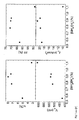
- the FIG. 1 explains the behavior of the solar cell parameters with variation of the silane concentration during the i-layer growth. At a certain silane concentration (here: - 0.9%) maximum efficiency is achieved. This silane concentration is not only important for solar cells, but is also the highest silane concentration at which under the given conditions microcrystalline silicon with a high crystalline volume fraction can be produced.
- FIG. 2 are the maximum silane flows at those with certain hydrogen flows in a continuous Process microcrystalline growth can be done and the resulting silane concentrations have been applied.
- the optimization was carried out according to FIG. 1 , With these combinations of silane and hydrogen flows, homogeneous growth of microcrystalline silicon layers (with a high crystalline volume fraction) is possible at the stated pressure and power.
- the FIG. 3 shows the quantum efficiency of a solar cell during which no more hydrogen was added during the deposition.
- the high quantum efficiency in the long-wave (> 800 nm) spectral range shows that the i-layer has a high crystalline volume fraction.
Landscapes
- Chemical & Material Sciences (AREA)
- Engineering & Computer Science (AREA)
- General Chemical & Material Sciences (AREA)
- Chemical Kinetics & Catalysis (AREA)
- Materials Engineering (AREA)
- Mechanical Engineering (AREA)
- Metallurgy (AREA)
- Organic Chemistry (AREA)
- Physics & Mathematics (AREA)
- Condensed Matter Physics & Semiconductors (AREA)
- General Physics & Mathematics (AREA)
- Manufacturing & Machinery (AREA)
- Computer Hardware Design (AREA)
- Microelectronics & Electronic Packaging (AREA)
- Power Engineering (AREA)
- Inorganic Chemistry (AREA)
- Plasma & Fusion (AREA)
- Photovoltaic Devices (AREA)
- Chemical Vapour Deposition (AREA)
- Crystals, And After-Treatments Of Crystals (AREA)
- Silicon Compounds (AREA)
Priority Applications (2)
| Application Number | Priority Date | Filing Date | Title |
|---|---|---|---|
| SI200430905T SI1601813T1 (sl) | 2003-02-27 | 2004-01-20 | Postopek za nanos silicija |
| CY20081101261T CY1108484T1 (el) | 2003-02-27 | 2008-11-06 | Μεθοδος για την αποθεση πυριτιου |
Applications Claiming Priority (3)
| Application Number | Priority Date | Filing Date | Title |
|---|---|---|---|
| DE10308381A DE10308381B4 (de) | 2003-02-27 | 2003-02-27 | Verfahren zur Abscheidung von Silizium |
| DE10308381 | 2003-02-27 | ||
| PCT/DE2004/000066 WO2004076713A1 (de) | 2003-02-27 | 2004-01-20 | Verfahren zur abscheidung von silizium |
Publications (2)
| Publication Number | Publication Date |
|---|---|
| EP1601813A1 EP1601813A1 (de) | 2005-12-07 |
| EP1601813B1 true EP1601813B1 (de) | 2008-08-06 |
Family
ID=32863924
Family Applications (1)
| Application Number | Title | Priority Date | Filing Date |
|---|---|---|---|
| EP04703337A Expired - Lifetime EP1601813B1 (de) | 2003-02-27 | 2004-01-20 | Verfahren zur abscheidung von silizium |
Country Status (15)
| Country | Link |
|---|---|
| US (1) | US7981776B2 (enExample) |
| EP (1) | EP1601813B1 (enExample) |
| JP (1) | JP4733627B2 (enExample) |
| KR (1) | KR101127047B1 (enExample) |
| CN (1) | CN1754007A (enExample) |
| AT (1) | ATE403763T1 (enExample) |
| AU (1) | AU2004215243B2 (enExample) |
| CA (1) | CA2517598C (enExample) |
| CY (1) | CY1108484T1 (enExample) |
| DE (2) | DE10308381B4 (enExample) |
| ES (1) | ES2311792T3 (enExample) |
| PT (1) | PT1601813E (enExample) |
| RU (1) | RU2005129984A (enExample) |
| SI (1) | SI1601813T1 (enExample) |
| WO (1) | WO2004076713A1 (enExample) |
Families Citing this family (14)
| Publication number | Priority date | Publication date | Assignee | Title |
|---|---|---|---|---|
| JP2006216624A (ja) * | 2005-02-01 | 2006-08-17 | Mitsubishi Heavy Ind Ltd | 太陽電池及び太陽電池の製造方法 |
| US8203071B2 (en) | 2007-01-18 | 2012-06-19 | Applied Materials, Inc. | Multi-junction solar cells and methods and apparatuses for forming the same |
| TWI350006B (en) * | 2007-10-05 | 2011-10-01 | Ind Tech Res Inst | Plasma enhanced thin film deposition method |
| JP2011503848A (ja) | 2007-11-02 | 2011-01-27 | アプライド マテリアルズ インコーポレイテッド | 堆積プロセス間のプラズマ処置 |
| JP5005588B2 (ja) | 2008-03-14 | 2012-08-22 | 東洋自動機株式会社 | 袋移送及び傾き修正装置 |
| RU2367600C1 (ru) * | 2008-04-16 | 2009-09-20 | Борис Георгиевич Грибов | Способ получения кремния высокой чистоты |
| DE102008063737A1 (de) * | 2008-12-18 | 2010-06-24 | Forschungszentrum Jülich GmbH | Verfahren zur Abscheidung von mikrokristallinem Silizium auf einem Substrat |
| TW201120942A (en) * | 2009-12-08 | 2011-06-16 | Ind Tech Res Inst | Method for depositing microcrystalline silicon and monitor device of a plasma enhanced deposition |
| CN102108494B (zh) * | 2009-12-23 | 2013-01-16 | 财团法人工业技术研究院 | 微晶硅薄膜的沉积方法及等离子体辅助沉积的监控装置 |
| CN102031503B (zh) * | 2010-09-29 | 2012-12-05 | 理想能源设备(上海)有限公司 | 硅薄膜的沉积方法 |
| US8642376B2 (en) * | 2011-05-16 | 2014-02-04 | Applied Materials, Inc. | Methods for depositing a material atop a substrate |
| DE102014007767B4 (de) * | 2014-05-21 | 2025-08-28 | Christian Bauch | Verfahren zur Herstellung halogenierter Oligosilane aus Silicium und Tetrachlorsilan |
| DE102014007766B4 (de) * | 2014-05-21 | 2025-10-16 | Christian Bauch | Verfahren zur plasmachemischen Herstellung halogenierter Oligosilane aus Tetrachlorsilan |
| CN114242833A (zh) * | 2021-11-18 | 2022-03-25 | 国家电投集团科学技术研究院有限公司 | 异质结太阳电池的硅片处理方法 |
Family Cites Families (9)
| Publication number | Priority date | Publication date | Assignee | Title |
|---|---|---|---|---|
| US5334423A (en) * | 1993-01-28 | 1994-08-02 | United Solar Systems Corp. | Microwave energized process for the preparation of high quality semiconductor material |
| JPH09232235A (ja) * | 1995-02-24 | 1997-09-05 | Mitsui Toatsu Chem Inc | 光電変換素子 |
| JPH1081973A (ja) | 1996-03-18 | 1998-03-31 | Hyundai Electron Ind Co Ltd | 誘導結合形プラズマcvd装置 |
| US5824940A (en) | 1997-01-27 | 1998-10-20 | Alfred University | Ceramic bullet-proof fabric |
| JPH11233801A (ja) * | 1998-02-17 | 1999-08-27 | Canon Inc | 微結晶シリコン膜の形成方法、および光起電力素子 |
| JP4335389B2 (ja) * | 1999-11-24 | 2009-09-30 | 株式会社カネカ | シリコン系薄膜光電変換装置の製造方法 |
| JP3857024B2 (ja) * | 2000-07-17 | 2006-12-13 | 株式会社神戸製鋼所 | 微結晶シリコン薄膜の形成方法 |
| JP2003007629A (ja) * | 2001-04-03 | 2003-01-10 | Canon Inc | シリコン系膜の形成方法、シリコン系膜および半導体素子 |
| JP4397391B2 (ja) * | 2006-10-30 | 2010-01-13 | 信越フィルム株式会社 | ガスバリア性プラスチックおよびプラスチックフィルムの製造方法 |
-
2003
- 2003-02-27 DE DE10308381A patent/DE10308381B4/de not_active Expired - Lifetime
-
2004
- 2004-01-20 DE DE502004007776T patent/DE502004007776D1/de not_active Expired - Lifetime
- 2004-01-20 ES ES04703337T patent/ES2311792T3/es not_active Expired - Lifetime
- 2004-01-20 SI SI200430905T patent/SI1601813T1/sl unknown
- 2004-01-20 CA CA2517598A patent/CA2517598C/en not_active Expired - Fee Related
- 2004-01-20 PT PT04703337T patent/PT1601813E/pt unknown
- 2004-01-20 US US10/547,118 patent/US7981776B2/en not_active Expired - Fee Related
- 2004-01-20 EP EP04703337A patent/EP1601813B1/de not_active Expired - Lifetime
- 2004-01-20 AT AT04703337T patent/ATE403763T1/de active
- 2004-01-20 WO PCT/DE2004/000066 patent/WO2004076713A1/de not_active Ceased
- 2004-01-20 RU RU2005129984/02A patent/RU2005129984A/ru not_active Application Discontinuation
- 2004-01-20 JP JP2006501464A patent/JP4733627B2/ja not_active Expired - Fee Related
- 2004-01-20 AU AU2004215243A patent/AU2004215243B2/en not_active Ceased
- 2004-01-20 CN CNA2004800052636A patent/CN1754007A/zh active Pending
- 2004-01-20 KR KR1020057015528A patent/KR101127047B1/ko not_active Expired - Fee Related
-
2008
- 2008-11-06 CY CY20081101261T patent/CY1108484T1/el unknown
Also Published As
| Publication number | Publication date |
|---|---|
| EP1601813A1 (de) | 2005-12-07 |
| ES2311792T3 (es) | 2009-02-16 |
| CA2517598C (en) | 2012-05-15 |
| JP4733627B2 (ja) | 2011-07-27 |
| SI1601813T1 (sl) | 2009-02-28 |
| DE10308381B4 (de) | 2012-08-16 |
| WO2004076713A1 (de) | 2004-09-10 |
| AU2004215243B2 (en) | 2009-12-03 |
| DE10308381A1 (de) | 2004-09-16 |
| KR20050114218A (ko) | 2005-12-05 |
| US20060240649A1 (en) | 2006-10-26 |
| CY1108484T1 (el) | 2014-04-09 |
| CA2517598A1 (en) | 2004-09-10 |
| AU2004215243A1 (en) | 2004-09-10 |
| DE502004007776D1 (de) | 2008-09-18 |
| RU2005129984A (ru) | 2006-05-10 |
| PT1601813E (pt) | 2008-11-13 |
| CN1754007A (zh) | 2006-03-29 |
| ATE403763T1 (de) | 2008-08-15 |
| US7981776B2 (en) | 2011-07-19 |
| KR101127047B1 (ko) | 2012-04-23 |
| JP2006519482A (ja) | 2006-08-24 |
Similar Documents
| Publication | Publication Date | Title |
|---|---|---|
| EP1601813B1 (de) | Verfahren zur abscheidung von silizium | |
| DE69636253T2 (de) | Verfahren zur Herstellung einer Silizium Solarzelle und so hergestellte Solarzelle | |
| DE69331522T2 (de) | Mikrowellengespeistes abscheideverfahren mit regelung der substrattemperatur. | |
| DE102010000002B4 (de) | Verfahren zur Abscheidung von Mehrlagenschichten und/oder Gradientenschichten | |
| DE69021960T2 (de) | Verfahren zur kontinuierlichen Herstellung von einem grossflächigen funktionellen aufgedampften Film mittels Mikrowellen-Plasma-CVD sowie Anlage zur Durchführung des Verfahrens. | |
| DE69213759T2 (de) | Halbleiter vorrichtung und herstellungsverfahren mittels mikrowellen-niederschlag. | |
| DE69125554T2 (de) | Verfahren zur Herstellung einer Solarzelle aus amorphem Silizium | |
| DE3135393A1 (de) | Verfahren zum herstellen einer lichtempfindlichen amorphen legierung und diese enthaltendes bauelement | |
| DE19844102A1 (de) | Herstellverfahren für eine Halbleiterstruktur | |
| DE102010000001A1 (de) | Inline-Beschichtungsanlage | |
| DE3742110A1 (de) | Verfahren zur bildung funktioneller aufgedampfter filme durch ein chemisches mikrowellen-plasma-aufdampfverfahren | |
| DE112009002455T5 (de) | Plasma-CVD-Vorrichtung, Verfahren zum Herstellen einer Halbleiterschicht, Verfahren zum Herstellen einer Dünnschichtsolarzelle und Verfahren zum Reinigen einer Plasma-CVD-Vorrichtung | |
| EP0949688A1 (de) | Dünnschichtsolarzelle, Verfahren zu deren Herstellung sowie Vorrichtung zur Durchführung des Verfahrens | |
| EP0224231B1 (de) | Verfahren zur Herstellung einer Dünnschichtssolarzelle | |
| DE3644655A1 (de) | Verfahren zur bildung eines abgeschiedenen films | |
| DE69633754T2 (de) | Herstellungsverfahren für einen dünnen Halbleiterfilm | |
| EP1829117A1 (de) | Verfahren zur herstellung einer dünnschichtsolarzelle mit mikrokristallinem silizium sowie schichtfolge | |
| EP1706908B1 (de) | Herstellungsverfahren für stapelsolarzellen umfassend mikrokristallinem siliziumschichten | |
| DE69501624T2 (de) | Plasmabearbeitungsverfahren und Plasmabearbeitungsgerät | |
| EP1110248B1 (en) | Method for depositing layers of high quality semiconductor material | |
| EP1187945B1 (de) | Verfahren zur plasmaunterstützten reaktiven abscheidung von material | |
| DE3441044C2 (enExample) | ||
| DE102008063737A1 (de) | Verfahren zur Abscheidung von mikrokristallinem Silizium auf einem Substrat | |
| DE3781748T2 (de) | Beschichtungssystem, bestehend aus mehreren kammern. | |
| DE69013965T2 (de) | Methode zur Bildung einer dünnen Halbleiterschicht. |
Legal Events
| Date | Code | Title | Description |
|---|---|---|---|
| PUAI | Public reference made under article 153(3) epc to a published international application that has entered the european phase |
Free format text: ORIGINAL CODE: 0009012 |
|
| 17P | Request for examination filed |
Effective date: 20050727 |
|
| AK | Designated contracting states |
Kind code of ref document: A1 Designated state(s): AT BE BG CH CY CZ DE DK EE ES FI FR GB GR HU IE IT LI LU MC NL PT RO SE SI SK TR |
|
| AX | Request for extension of the european patent |
Extension state: AL LT LV MK |
|
| RIN1 | Information on inventor provided before grant (corrected) |
Inventor name: RECH, BERND Inventor name: ROSCHEK, TOBIAS |
|
| DAX | Request for extension of the european patent (deleted) | ||
| 17Q | First examination report despatched |
Effective date: 20051222 |
|
| GRAP | Despatch of communication of intention to grant a patent |
Free format text: ORIGINAL CODE: EPIDOSNIGR1 |
|
| GRAS | Grant fee paid |
Free format text: ORIGINAL CODE: EPIDOSNIGR3 |
|
| GRAA | (expected) grant |
Free format text: ORIGINAL CODE: 0009210 |
|
| AK | Designated contracting states |
Kind code of ref document: B1 Designated state(s): AT BE BG CH CY CZ DE DK EE ES FI FR GB GR HU IE IT LI LU MC NL PT RO SE SI SK TR |
|
| REG | Reference to a national code |
Ref country code: GB Ref legal event code: FG4D Free format text: NOT ENGLISH |
|
| REG | Reference to a national code |
Ref country code: CH Ref legal event code: EP |
|
| REG | Reference to a national code |
Ref country code: IE Ref legal event code: FG4D Free format text: LANGUAGE OF EP DOCUMENT: GERMAN |
|
| REF | Corresponds to: |
Ref document number: 502004007776 Country of ref document: DE Date of ref document: 20080918 Kind code of ref document: P |
|
| REG | Reference to a national code |
Ref country code: RO Ref legal event code: EPE |
|
| REG | Reference to a national code |
Ref country code: PT Ref legal event code: SC4A Free format text: AVAILABILITY OF NATIONAL TRANSLATION Effective date: 20081103 |
|
| REG | Reference to a national code |
Ref country code: GR Ref legal event code: EP Ref document number: 20080403014 Country of ref document: GR |
|
| PG25 | Lapsed in a contracting state [announced via postgrant information from national office to epo] |
Ref country code: NL Free format text: LAPSE BECAUSE OF FAILURE TO SUBMIT A TRANSLATION OF THE DESCRIPTION OR TO PAY THE FEE WITHIN THE PRESCRIBED TIME-LIMIT Effective date: 20080806 |
|
| REG | Reference to a national code |
Ref country code: ES Ref legal event code: FG2A Ref document number: 2311792 Country of ref document: ES Kind code of ref document: T3 |
|
| PG25 | Lapsed in a contracting state [announced via postgrant information from national office to epo] |
Ref country code: FI Free format text: LAPSE BECAUSE OF FAILURE TO SUBMIT A TRANSLATION OF THE DESCRIPTION OR TO PAY THE FEE WITHIN THE PRESCRIBED TIME-LIMIT Effective date: 20080806 |
|
| REG | Reference to a national code |
Ref country code: IE Ref legal event code: FD4D |
|
| PG25 | Lapsed in a contracting state [announced via postgrant information from national office to epo] |
Ref country code: DK Free format text: LAPSE BECAUSE OF FAILURE TO SUBMIT A TRANSLATION OF THE DESCRIPTION OR TO PAY THE FEE WITHIN THE PRESCRIBED TIME-LIMIT Effective date: 20080806 Ref country code: IE Free format text: LAPSE BECAUSE OF FAILURE TO SUBMIT A TRANSLATION OF THE DESCRIPTION OR TO PAY THE FEE WITHIN THE PRESCRIBED TIME-LIMIT Effective date: 20080806 |
|
| REG | Reference to a national code |
Ref country code: HU Ref legal event code: AG4A Ref document number: E004841 Country of ref document: HU |
|
| PLBE | No opposition filed within time limit |
Free format text: ORIGINAL CODE: 0009261 |
|
| STAA | Information on the status of an ep patent application or granted ep patent |
Free format text: STATUS: NO OPPOSITION FILED WITHIN TIME LIMIT |
|
| 26N | No opposition filed |
Effective date: 20090507 |
|
| PG25 | Lapsed in a contracting state [announced via postgrant information from national office to epo] |
Ref country code: EE Free format text: LAPSE BECAUSE OF FAILURE TO SUBMIT A TRANSLATION OF THE DESCRIPTION OR TO PAY THE FEE WITHIN THE PRESCRIBED TIME-LIMIT Effective date: 20080806 |
|
| PG25 | Lapsed in a contracting state [announced via postgrant information from national office to epo] |
Ref country code: MC Free format text: LAPSE BECAUSE OF NON-PAYMENT OF DUE FEES Effective date: 20090131 |
|
| PG25 | Lapsed in a contracting state [announced via postgrant information from national office to epo] |
Ref country code: SE Free format text: LAPSE BECAUSE OF FAILURE TO SUBMIT A TRANSLATION OF THE DESCRIPTION OR TO PAY THE FEE WITHIN THE PRESCRIBED TIME-LIMIT Effective date: 20081106 |
|
| PG25 | Lapsed in a contracting state [announced via postgrant information from national office to epo] |
Ref country code: BE Free format text: LAPSE BECAUSE OF NON-PAYMENT OF DUE FEES Effective date: 20090131 |
|
| PG25 | Lapsed in a contracting state [announced via postgrant information from national office to epo] |
Ref country code: LU Free format text: LAPSE BECAUSE OF NON-PAYMENT OF DUE FEES Effective date: 20090120 |
|
| PGFP | Annual fee paid to national office [announced via postgrant information from national office to epo] |
Ref country code: TR Payment date: 20120110 Year of fee payment: 9 |
|
| PGFP | Annual fee paid to national office [announced via postgrant information from national office to epo] |
Ref country code: CZ Payment date: 20130110 Year of fee payment: 10 Ref country code: GB Payment date: 20130122 Year of fee payment: 10 Ref country code: CH Payment date: 20130123 Year of fee payment: 10 Ref country code: HU Payment date: 20130116 Year of fee payment: 10 Ref country code: BG Payment date: 20130123 Year of fee payment: 10 Ref country code: RO Payment date: 20130115 Year of fee payment: 10 |
|
| PGFP | Annual fee paid to national office [announced via postgrant information from national office to epo] |
Ref country code: GR Payment date: 20130121 Year of fee payment: 10 Ref country code: SI Payment date: 20130109 Year of fee payment: 10 Ref country code: SK Payment date: 20130111 Year of fee payment: 10 Ref country code: CY Payment date: 20130114 Year of fee payment: 10 |
|
| PGFP | Annual fee paid to national office [announced via postgrant information from national office to epo] |
Ref country code: AT Payment date: 20130121 Year of fee payment: 10 Ref country code: PT Payment date: 20130111 Year of fee payment: 10 |
|
| REG | Reference to a national code |
Ref country code: PT Ref legal event code: MM4A Free format text: LAPSE DUE TO NON-PAYMENT OF FEES Effective date: 20140721 |
|
| REG | Reference to a national code |
Ref country code: CH Ref legal event code: PL |
|
| REG | Reference to a national code |
Ref country code: AT Ref legal event code: MM01 Ref document number: 403763 Country of ref document: AT Kind code of ref document: T Effective date: 20140120 |
|
| GBPC | Gb: european patent ceased through non-payment of renewal fee |
Effective date: 20140120 |
|
| REG | Reference to a national code |
Ref country code: SK Ref legal event code: MM4A Ref document number: E 4354 Country of ref document: SK Effective date: 20140120 |
|
| REG | Reference to a national code |
Ref country code: GR Ref legal event code: ML Ref document number: 20080403014 Country of ref document: GR Effective date: 20140801 |
|
| REG | Reference to a national code |
Ref country code: SI Ref legal event code: KO00 Effective date: 20140909 |
|
| PG25 | Lapsed in a contracting state [announced via postgrant information from national office to epo] |
Ref country code: RO Free format text: LAPSE BECAUSE OF NON-PAYMENT OF DUE FEES Effective date: 20140120 Ref country code: GR Free format text: LAPSE BECAUSE OF NON-PAYMENT OF DUE FEES Effective date: 20140801 Ref country code: LI Free format text: LAPSE BECAUSE OF NON-PAYMENT OF DUE FEES Effective date: 20140131 Ref country code: BG Free format text: LAPSE BECAUSE OF NON-PAYMENT OF DUE FEES Effective date: 20140930 Ref country code: CH Free format text: LAPSE BECAUSE OF NON-PAYMENT OF DUE FEES Effective date: 20140131 Ref country code: CY Free format text: LAPSE BECAUSE OF NON-PAYMENT OF DUE FEES Effective date: 20140120 Ref country code: CZ Free format text: LAPSE BECAUSE OF NON-PAYMENT OF DUE FEES Effective date: 20140120 |
|
| PG25 | Lapsed in a contracting state [announced via postgrant information from national office to epo] |
Ref country code: GB Free format text: LAPSE BECAUSE OF NON-PAYMENT OF DUE FEES Effective date: 20140120 Ref country code: SK Free format text: LAPSE BECAUSE OF NON-PAYMENT OF DUE FEES Effective date: 20140120 Ref country code: HU Free format text: LAPSE BECAUSE OF NON-PAYMENT OF DUE FEES Effective date: 20140121 Ref country code: AT Free format text: LAPSE BECAUSE OF NON-PAYMENT OF DUE FEES Effective date: 20140120 Ref country code: SI Free format text: LAPSE BECAUSE OF NON-PAYMENT OF DUE FEES Effective date: 20140121 |
|
| PG25 | Lapsed in a contracting state [announced via postgrant information from national office to epo] |
Ref country code: PT Free format text: LAPSE BECAUSE OF NON-PAYMENT OF DUE FEES Effective date: 20140721 |
|
| REG | Reference to a national code |
Ref country code: FR Ref legal event code: PLFP Year of fee payment: 12 |
|
| PGFP | Annual fee paid to national office [announced via postgrant information from national office to epo] |
Ref country code: ES Payment date: 20150122 Year of fee payment: 12 |
|
| PGFP | Annual fee paid to national office [announced via postgrant information from national office to epo] |
Ref country code: FR Payment date: 20150115 Year of fee payment: 12 |
|
| REG | Reference to a national code |
Ref country code: FR Ref legal event code: ST Effective date: 20160930 |
|
| PG25 | Lapsed in a contracting state [announced via postgrant information from national office to epo] |
Ref country code: FR Free format text: LAPSE BECAUSE OF NON-PAYMENT OF DUE FEES Effective date: 20160201 |
|
| REG | Reference to a national code |
Ref country code: ES Ref legal event code: FD2A Effective date: 20170224 |
|
| PGFP | Annual fee paid to national office [announced via postgrant information from national office to epo] |
Ref country code: DE Payment date: 20161215 Year of fee payment: 14 |
|
| PG25 | Lapsed in a contracting state [announced via postgrant information from national office to epo] |
Ref country code: ES Free format text: LAPSE BECAUSE OF NON-PAYMENT OF DUE FEES Effective date: 20160121 |
|
| PGFP | Annual fee paid to national office [announced via postgrant information from national office to epo] |
Ref country code: IT Payment date: 20170125 Year of fee payment: 14 |
|
| PG25 | Lapsed in a contracting state [announced via postgrant information from national office to epo] |
Ref country code: TR Free format text: LAPSE BECAUSE OF NON-PAYMENT OF DUE FEES Effective date: 20140120 |
|
| REG | Reference to a national code |
Ref country code: DE Ref legal event code: R119 Ref document number: 502004007776 Country of ref document: DE |
|
| PG25 | Lapsed in a contracting state [announced via postgrant information from national office to epo] |
Ref country code: DE Free format text: LAPSE BECAUSE OF NON-PAYMENT OF DUE FEES Effective date: 20180801 |
|
| PG25 | Lapsed in a contracting state [announced via postgrant information from national office to epo] |
Ref country code: IT Free format text: LAPSE BECAUSE OF NON-PAYMENT OF DUE FEES Effective date: 20180120 |