EP1601813B1 - Verfahren zur abscheidung von silizium - Google Patents
Verfahren zur abscheidung von silizium Download PDFInfo
- Publication number
- EP1601813B1 EP1601813B1 EP04703337A EP04703337A EP1601813B1 EP 1601813 B1 EP1601813 B1 EP 1601813B1 EP 04703337 A EP04703337 A EP 04703337A EP 04703337 A EP04703337 A EP 04703337A EP 1601813 B1 EP1601813 B1 EP 1601813B1
- Authority
- EP
- European Patent Office
- Prior art keywords
- plasma
- chamber
- hydrogen
- sccm
- deposition
- Prior art date
- Legal status (The legal status is an assumption and is not a legal conclusion. Google has not performed a legal analysis and makes no representation as to the accuracy of the status listed.)
- Expired - Lifetime
Links
- 238000000151 deposition Methods 0.000 title claims abstract description 54
- 238000000034 method Methods 0.000 title claims abstract description 48
- 229910052710 silicon Inorganic materials 0.000 title claims abstract description 28
- 239000010703 silicon Substances 0.000 title claims abstract description 27
- UFHFLCQGNIYNRP-UHFFFAOYSA-N Hydrogen Chemical compound [H][H] UFHFLCQGNIYNRP-UHFFFAOYSA-N 0.000 claims abstract description 56
- 239000001257 hydrogen Substances 0.000 claims abstract description 54
- 229910052739 hydrogen Inorganic materials 0.000 claims abstract description 54
- 239000007789 gas Substances 0.000 claims abstract description 43
- XUIMIQQOPSSXEZ-UHFFFAOYSA-N Silicon Chemical compound [Si] XUIMIQQOPSSXEZ-UHFFFAOYSA-N 0.000 claims abstract description 27
- 239000000203 mixture Substances 0.000 claims abstract description 16
- 229910021424 microcrystalline silicon Inorganic materials 0.000 claims abstract description 15
- 239000000758 substrate Substances 0.000 claims abstract description 12
- 230000008021 deposition Effects 0.000 claims description 48
- BLRPTPMANUNPDV-UHFFFAOYSA-N Silane Chemical compound [SiH4] BLRPTPMANUNPDV-UHFFFAOYSA-N 0.000 claims description 45
- 229910000077 silane Inorganic materials 0.000 claims description 37
- 230000005284 excitation Effects 0.000 claims description 8
- 239000006096 absorbing agent Substances 0.000 claims description 4
- 230000001105 regulatory effect Effects 0.000 claims description 2
- 230000000977 initiatory effect Effects 0.000 abstract 2
- 239000011248 coating agent Substances 0.000 description 12
- 238000000576 coating method Methods 0.000 description 12
- 238000000623 plasma-assisted chemical vapour deposition Methods 0.000 description 9
- 239000000463 material Substances 0.000 description 5
- 230000003068 static effect Effects 0.000 description 5
- 229910021417 amorphous silicon Inorganic materials 0.000 description 4
- 238000005137 deposition process Methods 0.000 description 4
- 150000002431 hydrogen Chemical class 0.000 description 4
- 238000004519 manufacturing process Methods 0.000 description 4
- 238000010924 continuous production Methods 0.000 description 3
- 239000010409 thin film Substances 0.000 description 3
- 229910021419 crystalline silicon Inorganic materials 0.000 description 2
- 230000004907 flux Effects 0.000 description 2
- 238000005457 optimization Methods 0.000 description 2
- 238000005086 pumping Methods 0.000 description 2
- 150000004756 silanes Chemical class 0.000 description 2
- 229910003902 SiCl 4 Inorganic materials 0.000 description 1
- 125000004429 atom Chemical group 0.000 description 1
- 230000015572 biosynthetic process Effects 0.000 description 1
- 125000004122 cyclic group Chemical group 0.000 description 1
- 238000000354 decomposition reaction Methods 0.000 description 1
- 230000007423 decrease Effects 0.000 description 1
- 230000006735 deficit Effects 0.000 description 1
- 230000001419 dependent effect Effects 0.000 description 1
- MROCJMGDEKINLD-UHFFFAOYSA-N dichlorosilane Chemical compound Cl[SiH2]Cl MROCJMGDEKINLD-UHFFFAOYSA-N 0.000 description 1
- 239000012895 dilution Substances 0.000 description 1
- 238000010790 dilution Methods 0.000 description 1
- PZPGRFITIJYNEJ-UHFFFAOYSA-N disilane Chemical compound [SiH3][SiH3] PZPGRFITIJYNEJ-UHFFFAOYSA-N 0.000 description 1
- 230000000694 effects Effects 0.000 description 1
- 238000005530 etching Methods 0.000 description 1
- 125000004435 hydrogen atom Chemical group [H]* 0.000 description 1
- 238000011534 incubation Methods 0.000 description 1
- 238000009776 industrial production Methods 0.000 description 1
- -1 silane hydrogen Chemical class 0.000 description 1
- 239000000243 solution Substances 0.000 description 1
- 230000003595 spectral effect Effects 0.000 description 1
Images

Classifications
-
- H—ELECTRICITY
- H01—ELECTRIC ELEMENTS
- H01L—SEMICONDUCTOR DEVICES NOT COVERED BY CLASS H10
- H01L21/00—Processes or apparatus adapted for the manufacture or treatment of semiconductor or solid state devices or of parts thereof
- H01L21/02—Manufacture or treatment of semiconductor devices or of parts thereof
- H01L21/02104—Forming layers
- H01L21/02365—Forming inorganic semiconducting materials on a substrate
- H01L21/02612—Formation types
- H01L21/02617—Deposition types
- H01L21/0262—Reduction or decomposition of gaseous compounds, e.g. CVD
-
- C—CHEMISTRY; METALLURGY
- C23—COATING METALLIC MATERIAL; COATING MATERIAL WITH METALLIC MATERIAL; CHEMICAL SURFACE TREATMENT; DIFFUSION TREATMENT OF METALLIC MATERIAL; COATING BY VACUUM EVAPORATION, BY SPUTTERING, BY ION IMPLANTATION OR BY CHEMICAL VAPOUR DEPOSITION, IN GENERAL; INHIBITING CORROSION OF METALLIC MATERIAL OR INCRUSTATION IN GENERAL
- C23C—COATING METALLIC MATERIAL; COATING MATERIAL WITH METALLIC MATERIAL; SURFACE TREATMENT OF METALLIC MATERIAL BY DIFFUSION INTO THE SURFACE, BY CHEMICAL CONVERSION OR SUBSTITUTION; COATING BY VACUUM EVAPORATION, BY SPUTTERING, BY ION IMPLANTATION OR BY CHEMICAL VAPOUR DEPOSITION, IN GENERAL
- C23C16/00—Chemical coating by decomposition of gaseous compounds, without leaving reaction products of surface material in the coating, i.e. chemical vapour deposition [CVD] processes
- C23C16/22—Chemical coating by decomposition of gaseous compounds, without leaving reaction products of surface material in the coating, i.e. chemical vapour deposition [CVD] processes characterised by the deposition of inorganic material, other than metallic material
- C23C16/24—Deposition of silicon only
-
- C—CHEMISTRY; METALLURGY
- C23—COATING METALLIC MATERIAL; COATING MATERIAL WITH METALLIC MATERIAL; CHEMICAL SURFACE TREATMENT; DIFFUSION TREATMENT OF METALLIC MATERIAL; COATING BY VACUUM EVAPORATION, BY SPUTTERING, BY ION IMPLANTATION OR BY CHEMICAL VAPOUR DEPOSITION, IN GENERAL; INHIBITING CORROSION OF METALLIC MATERIAL OR INCRUSTATION IN GENERAL
- C23C—COATING METALLIC MATERIAL; COATING MATERIAL WITH METALLIC MATERIAL; SURFACE TREATMENT OF METALLIC MATERIAL BY DIFFUSION INTO THE SURFACE, BY CHEMICAL CONVERSION OR SUBSTITUTION; COATING BY VACUUM EVAPORATION, BY SPUTTERING, BY ION IMPLANTATION OR BY CHEMICAL VAPOUR DEPOSITION, IN GENERAL
- C23C16/00—Chemical coating by decomposition of gaseous compounds, without leaving reaction products of surface material in the coating, i.e. chemical vapour deposition [CVD] processes
- C23C16/44—Chemical coating by decomposition of gaseous compounds, without leaving reaction products of surface material in the coating, i.e. chemical vapour deposition [CVD] processes characterised by the method of coating
- C23C16/455—Chemical coating by decomposition of gaseous compounds, without leaving reaction products of surface material in the coating, i.e. chemical vapour deposition [CVD] processes characterised by the method of coating characterised by the method used for introducing gases into reaction chamber or for modifying gas flows in reaction chamber
- C23C16/45557—Pulsed pressure or control pressure
-
- C—CHEMISTRY; METALLURGY
- C23—COATING METALLIC MATERIAL; COATING MATERIAL WITH METALLIC MATERIAL; CHEMICAL SURFACE TREATMENT; DIFFUSION TREATMENT OF METALLIC MATERIAL; COATING BY VACUUM EVAPORATION, BY SPUTTERING, BY ION IMPLANTATION OR BY CHEMICAL VAPOUR DEPOSITION, IN GENERAL; INHIBITING CORROSION OF METALLIC MATERIAL OR INCRUSTATION IN GENERAL
- C23C—COATING METALLIC MATERIAL; COATING MATERIAL WITH METALLIC MATERIAL; SURFACE TREATMENT OF METALLIC MATERIAL BY DIFFUSION INTO THE SURFACE, BY CHEMICAL CONVERSION OR SUBSTITUTION; COATING BY VACUUM EVAPORATION, BY SPUTTERING, BY ION IMPLANTATION OR BY CHEMICAL VAPOUR DEPOSITION, IN GENERAL
- C23C16/00—Chemical coating by decomposition of gaseous compounds, without leaving reaction products of surface material in the coating, i.e. chemical vapour deposition [CVD] processes
- C23C16/44—Chemical coating by decomposition of gaseous compounds, without leaving reaction products of surface material in the coating, i.e. chemical vapour deposition [CVD] processes characterised by the method of coating
- C23C16/50—Chemical coating by decomposition of gaseous compounds, without leaving reaction products of surface material in the coating, i.e. chemical vapour deposition [CVD] processes characterised by the method of coating using electric discharges
- C23C16/505—Chemical coating by decomposition of gaseous compounds, without leaving reaction products of surface material in the coating, i.e. chemical vapour deposition [CVD] processes characterised by the method of coating using electric discharges using radio frequency discharges
-
- H—ELECTRICITY
- H01—ELECTRIC ELEMENTS
- H01L—SEMICONDUCTOR DEVICES NOT COVERED BY CLASS H10
- H01L21/00—Processes or apparatus adapted for the manufacture or treatment of semiconductor or solid state devices or of parts thereof
- H01L21/02—Manufacture or treatment of semiconductor devices or of parts thereof
- H01L21/02104—Forming layers
- H01L21/02365—Forming inorganic semiconducting materials on a substrate
- H01L21/02518—Deposited layers
- H01L21/02521—Materials
- H01L21/02524—Group 14 semiconducting materials
- H01L21/02532—Silicon, silicon germanium, germanium
-
- H—ELECTRICITY
- H01—ELECTRIC ELEMENTS
- H01L—SEMICONDUCTOR DEVICES NOT COVERED BY CLASS H10
- H01L31/00—Semiconductor devices sensitive to infrared radiation, light, electromagnetic radiation of shorter wavelength or corpuscular radiation and specially adapted either for the conversion of the energy of such radiation into electrical energy or for the control of electrical energy by such radiation; Processes or apparatus specially adapted for the manufacture or treatment thereof or of parts thereof; Details thereof
- H01L31/18—Processes or apparatus specially adapted for the manufacture or treatment of these devices or of parts thereof
- H01L31/1804—Processes or apparatus specially adapted for the manufacture or treatment of these devices or of parts thereof comprising only elements of Group IV of the Periodic System
- H01L31/182—Special manufacturing methods for polycrystalline Si, e.g. Si ribbon, poly Si ingots, thin films of polycrystalline Si
- H01L31/1824—Special manufacturing methods for microcrystalline Si, uc-Si
-
- Y—GENERAL TAGGING OF NEW TECHNOLOGICAL DEVELOPMENTS; GENERAL TAGGING OF CROSS-SECTIONAL TECHNOLOGIES SPANNING OVER SEVERAL SECTIONS OF THE IPC; TECHNICAL SUBJECTS COVERED BY FORMER USPC CROSS-REFERENCE ART COLLECTIONS [XRACs] AND DIGESTS
- Y02—TECHNOLOGIES OR APPLICATIONS FOR MITIGATION OR ADAPTATION AGAINST CLIMATE CHANGE
- Y02E—REDUCTION OF GREENHOUSE GAS [GHG] EMISSIONS, RELATED TO ENERGY GENERATION, TRANSMISSION OR DISTRIBUTION
- Y02E10/00—Energy generation through renewable energy sources
- Y02E10/50—Photovoltaic [PV] energy
- Y02E10/545—Microcrystalline silicon PV cells
-
- Y—GENERAL TAGGING OF NEW TECHNOLOGICAL DEVELOPMENTS; GENERAL TAGGING OF CROSS-SECTIONAL TECHNOLOGIES SPANNING OVER SEVERAL SECTIONS OF THE IPC; TECHNICAL SUBJECTS COVERED BY FORMER USPC CROSS-REFERENCE ART COLLECTIONS [XRACs] AND DIGESTS
- Y02—TECHNOLOGIES OR APPLICATIONS FOR MITIGATION OR ADAPTATION AGAINST CLIMATE CHANGE
- Y02P—CLIMATE CHANGE MITIGATION TECHNOLOGIES IN THE PRODUCTION OR PROCESSING OF GOODS
- Y02P70/00—Climate change mitigation technologies in the production process for final industrial or consumer products
- Y02P70/50—Manufacturing or production processes characterised by the final manufactured product
Definitions
- the invention relates to a method for the deposition of microcrystalline silicon, in which only a small amount of hydrogen is needed.
- Microcrystalline silicon is a material which is used in particular as an absorber material in solar cells. It is today produced in many laboratories by means of the PECVD process (plasma-enhanced chemical vapor deposition) of silane and hydrogen. The addition of hydrogen, the so-called hydrogen dilution, is necessary to produce crystalline silicon at substrate temperatures below 500 ° C. These crystalline silicon layers consist of many microscopic crystallites - hence the name microcrystalline silicon.
- High quality layers of microcrystalline silicon can be deposited in different deposition regimes.
- the hydrogen is needed to influence the layer growth. However, only a small portion of the hydrogen used is incorporated into the produced silicon layer, typically less than 10%. The remaining hydrogen is pumped out. For a later industrial Production is the high hydrogen consumption, especially at deposition at 13.56 MHz, due to the high cost of a serious problem [1] .
- This investigated process runs cyclically (discontinuously) and essentially comprises two process steps.
- a small amount of the reactive process gas SiH 4 or a CH 4 / SiH 4 mixture
- This step serves to refresh the gas atmosphere after a process cycle.
- the plasma burns at low power (about 10 W), so that an ultra-thin silicon layer is deposited.
- both the pumping power from the chamber and the gas supply is interrupted in the chamber.
- the deposition pressure is increased and the silane concentration is lowered to -5%.
- the plasma now burns at about 60 W.
- the process gases are gradually decomposed and the deposited layer continues to grow.
- an opposite effect occurs.
- the layer is etched by H radicals. The etch rate decreases due to the Increasing proportion of hydrogen in the plasma continues to increase, until finally a balance between layer growth and etching is achieved.
- Atoms that are weakly bound are preferably etched, so that eventually a network with stronger bonds is formed.
- the entire deposition process takes place as a continuous sequence of these two steps (layer by layer) to the desired layer thickness. It is reported by a crystalline volume fraction of more than 90%. Due to the cyclic change of the process conditions, this process is very expensive. It differs fundamentally from the standard PECVD method, and is not yet suitable for use in industry. So far no solar cell has been realized with this method.
- VHFGD very high frequency glow discharge
- the deposition Since the deposition is started with a pure silane plasma and only added later by the decomposition of the silane hydrogen, the deposited layer has a pronounced amorphous incubation layer (- 10 nm) as a first layer. This can lead to a significant impairment of the function in the use of such layers in components, in particular in solar cells. Thus, in solar cells whose i-layer was produced by this process, only an efficiency of 2.5% could be achieved.
- the object of the invention is to provide a process for the production of microcrystalline silicon layers which, on the one hand, in the direction of layer growth, has a nearly homogeneous microcrystalline structure, ie. H. homogeneous structural properties, and in which on the other hand only small amounts of hydrogen are used.
- homogeneous microcrystalline silicon layers in particular as a first layer on a substrate in a plasma deposition chamber, can only take place in the presence of corresponding amounts of hydrogen. This means that even at the beginning of a deposition hydrogen must be present, so that a crystalline growth can be advantageous from the beginning.
- a method has been developed in order to provide sufficient hydrogen at a low total hydrogen consumption from the beginning of the deposition. In the continuous process advantageously only small amounts of hydrogen are used.
- static deposition conditions are set during the deposition process. This is done inter alia by a regulated supply and discharge of the corresponding gases in and out of the plasma chamber.
- a ratio of reactive, silicon-containing gas to hydrogen of less than 0.5, in particular of less than 0.25 has proven to be advantageous.
- reactive, silicon-containing gas is particularly silane mentioned.
- dichlorosilane (SiCl 2 H 2 ) are also conceivable.
- the excitation frequency for the plasma is less than 50 MHz, in particular less than 30 MHz. For example, when using PECVD, the standard industry frequency of 13.56 MHz is used.
- a first embodiment of the method provides initially to present a mixture of hydrogen and a reactive silicon-containing gas, in particular silane, as an initial condition within the deposition chamber. This can be done, for example, both by a) the continuous flow through the plasma chamber with a corresponding gas mixture of silane and hydrogen, or else b) by a single flooding of the previously evacuated plasma chamber with a gas mixture. Simultaneously with the plasma start, the hydrogen supply is then stopped in case a).
- the plasma dissociated by the plasma and consumed by the deposition silane is replaced by continuous addition into the chamber after the plasma.
- a corresponding amount of the gas mixture present there is accordingly removed from the chamber in each case.
- the microcrystalline growth of the silicon layers on the substrate occurs from the beginning.
- the gas flows to be set depend on the respective size of the plasma chamber, in the context of this invention the gas flows are respectively related to the substrate surface to be coated.
- the gas flows for the reactive, silicon-containing gas set after the plasma start are advantageously in the range between 0.5 and 20 sccm / 100 cm 2 coating area, in particular in the range between 0.5 and 5 sccm / 100 cm 2 coating area.
- the plasma chamber having the substrate is continuously supplied with a mixture of reactive, silicon-containing gas and hydrogen.
- the plasma is started and the desired microcrystalline deposition of the silicon on the substrate takes place as desired.
- a respective amount of the gas mixture present there is removed from the chamber.
- Both the total gas flow and the ratio of reactive, silicon-containing gas to hydrogen are advantageously kept constant throughout the deposition. Typical total fluxes are in the range below 20 sccm / 100 cm 2 coating area, especially in the area below 6 sccm / 100 cm 2 coating area.
- the set ratio of reactive, silicon-containing gas and hydrogen is advantageously in the range above 15%, in particular above 19%.
- silane concentration above 3% at an excitation frequency of 13.56 MHz for the plasma, in particular of above 10% for all major excitation frequencies of the plasma.
- the inventive method makes it possible to produce homogeneous, microcrystalline silicon layers in a simple manner, which have been found to be outstandingly suitable in particular for use as absorber layers in solar cells. Particular attention is paid to the possibility with this method even in the narrow process window that for solar cells with high efficiency is necessary to deposit suitable layers.
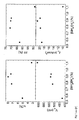
- the FIG. 1 explains the behavior of the solar cell parameters with variation of the silane concentration during the i-layer growth. At a certain silane concentration (here: - 0.9%) maximum efficiency is achieved. This silane concentration is not only important for solar cells, but is also the highest silane concentration at which under the given conditions microcrystalline silicon with a high crystalline volume fraction can be produced.
- FIG. 2 are the maximum silane flows at those with certain hydrogen flows in a continuous Process microcrystalline growth can be done and the resulting silane concentrations have been applied.
- the optimization was carried out according to FIG. 1 , With these combinations of silane and hydrogen flows, homogeneous growth of microcrystalline silicon layers (with a high crystalline volume fraction) is possible at the stated pressure and power.
- the FIG. 3 shows the quantum efficiency of a solar cell during which no more hydrogen was added during the deposition.
- the high quantum efficiency in the long-wave (> 800 nm) spectral range shows that the i-layer has a high crystalline volume fraction.
Description
- Die Erfindung betrifft ein Verfahren zur Abscheidung von mikrokristallinem Silizium, bei dem nur wenig Wasserstoff benötigt wird.
- Mikrokristallines Silizium ist ein Material, welches insbesondere in Solarzellen als Absorbermaterial genutzt wird. Es wird heute in vielen Labors mittels des PECVD-Verfahrens (plasma enhanced chemical vapor deposition) aus Silan und Wasserstoff hergestellt. Die Zugabe von Wasserstoff, die sogenannte Wasserstoffverdünnung, ist dabei notwendig um kristallines Silizium bei Substrattemperaturen unter 500°C herzustellen. Diese kristallinen Siliziumschichten bestehen aus vielen mikroskopisch kleinen Kristalliten - daher der Name mikrokristallines Silizium.
- Es können in verschiedenen Depositionsregimen qualitativ hochwertige Schichten aus mikrokristallinem Silizium abgeschieden werden. Bei der Abscheidung mit PECVD bei der Standardindustriefrequenz 13,56 MHz beträgt die Silankonzentration (=Silanfluss/Wasserstofffluss) typischerweise ca. 1 %, bei Anregungsfrequenzen im VHF-Bereich in der Regel weniger als 10%. Der Wasserstoff wird benötigt um das Schichtwachstum zu beeinflussen. Es wird jedoch nur ein geringer Teil des eingesetzten Wasserstoffs in die hergestellte Siliziumschicht eingebaut, typischerweise weniger als 10 %. Der übrige Wasserstoff wird abgepumpt. Für eine spätere industrielle Produktion ist der hohe Wasserstoffverbrauch, insbesondere bei Abscheidung bei 13,56 MHz, aufgrund der hohen Kosten ein ernsthaftes Problem[1].
- Aus dem Stand der Technik sind inzwischen die folgenden verbesserten Methoden zur Abscheidung von mikrokristallinem Silizium mittels PECVD mit geringem Wasserstoffverbrauch bekannt.
- Dieser untersuchte Prozess verläuft zyklisch (diskontinuierlich) und umfasst im wesentlichen zwei Prozessschritte. In einem ersten Schritt fließt eine geringe Menge des reaktiven Prozessgas (SiH4 oder eine CH4/SiH4-Mischung) in einem Verhältnis von ca. 25 % reaktivem Gas zu Wasserstoff durch die Kammer. Dieser Schritt dient der Auffrischung der Gasatmosphäre nach einem Prozesszyklus. Während dieser Zeit brennt das Plasma bei geringer Leistung (ca. 10 W), so dass eine ultra dünne Siliziumschicht abgeschieden wird.
- Im nachfolgenden zweiten Schritt wird sowohl die Pumpleistung aus der Kammer als auch die Gasversorgung in die Kammer unterbrochen. Durch eine Verzögerung des Abschaltens der Wasserstoffzufuhr wird der Depositionsdruck erhöht und die Silankonzentration auf -5 % erniedrigt. Das Plasma brennt nun bei ca. 60 W weiter. Die Prozessgase werden allmählich zersetzt und die abgeschiedene Schicht wächst weiter. Zur gleichen Zeit tritt ein gegensätzlicher Effekt auf. Die Schicht wird durch H-Radikale geätzt. Die Ätzrate nimmt aufgrund des steigenden Anteils an Wasserstoff im Plasma immer weiter zu, bis schließlich ein Gleichgewicht zwischen Schichtwachstum und Ätzen erreicht ist. Atome die schwach gebunden sind werden bevorzugt geätzt, so dass sich schließlich ein Netzwerk mit stärkeren Bindungen ausbildet.
- Der gesamte Abscheidungsprozess erfolgt als ständige Abfolge dieser beiden Schritte (layer by layer) bis zur gewünschten Schichtdicke. Es wird von einem kristallinen Volumenanteil von mehr als 90 % berichtet. Durch die zyklische Veränderung der Prozessbedingungen ist dieser Prozess jedoch sehr aufwendig. Er unterscheidet sich grundsätzlich von dem standardmäßig eingesetzten PECVD-Verfahren, und ist bislang noch nicht für den Einsatz in der Industrie geeignet. Mit diesem Verfahren konnte bisher auch noch keine Solarzelle realisiert werden.
- Dieses "very high frequency glow discharge" (VHFGD) Abscheidungsverfahren ist ein kontinuierlicher Prozess ohne jegliche Einsatz von Wasserstoff. Die Depositionskammer (Plasmakammer) ist nicht vollständig isoliert. Ein geringer Silanfluss wird in die Kammer eingelassen und eine entsprechende Menge Gas wird gleichzeitig abgepumpt. Die Abscheidung erfolgt bei VHF-Anregung und bei niedrigem Druck (0,1 mbar). Bei der Abscheidung von Silizium aus Silan wird Wasserstoff frei. Der geringe Silangasfluss sorgt dafür, dass eine Silanverarmung auftritt. Die anfänglich schnelle Abscheidung des Siliziums wird durch die Zunahme an dissoziiertem Wasserstoff gebremst. Nach ca. einer Minute herrschen statische Bedingungen mit einem kleinen Verhältnis von [SiH*]/[Hα] vor, bei denen ein kontinuierliches mikrokristallines Wachstum ermöglicht wird.
- Da die Abscheidung mit einem reinen Silanplasma gestartet wird und erst später durch die Zersetzung des Silans Wasserstoff hinzukommt, weist die abgeschiedene Schicht eine ausgeprägte amorphe Inkubationsschicht (- 10 nm) als erste Schicht auf. Das kann bei dem Einsatz solcher Schichten in Bauelementen, insbesondere in Solarzellen, zu einer deutlichen Beeinträchtigung der Funktion führen. So konnte bei Solarzellen deren i-Schicht mit diesem Verfahren hergestellt wurden, nur ein Wirkungsgrad von 2,5 % erzielt werden.
- Aus Rech et al. (B. Rech, O. Kluth, T. Repmann, T. Roschek, J. Springer, J. Müller, F. Finger, H. Stiebig, H. Wagner (2002). New materials and deposition techniques for highly efficient silicon thin film solar cells. Solar Energy Materials & Solar Cells 74 (2002) 439-447) ist ein PECVD-Verfahren für die Herstellung von µC-Si:H-Solarzellen bekannt.
- Repmann et al. (T. Repmann, W. Appenzeller, T. Roschek, B. Rech, O. Kluth, J. Müller, (2001). Development of a-Si:H/µC-Si:H thin film solar mudules using 13.56 MHz PECVD. 17th Europaen Photovoltaic Solar Energy Conference, 22-26 October 2001, Munich, Germany, Seiten 2836-2841) offenbaren die Entwicklung von Dünnfilmsolarzellenmodulen mit a-Si:H/µC-Si:H-Schichten mittels eines PECVD-Verfahrens bei 13,56 MHz Anregungsfrequenz.
- Aus Rech et al. (B. Rech, T. Roschek, J. Müller, S. Wieder, H. Wagner (2001). Amorphous and microcrystalline silicon solar cells prepared at high deposition rates using RF (13.56MHz) plasma excitation frequencies. Solar Energy Materials & Solar Cells 66 (2001) 267-273) ist ein weiteres Verfahren zur Abscheidung von mikrokristallinen und amorphen Silizium für Solarzellen bei hohen Depositionsraten bekannt.
- Nachteilig sind auch bei diesen Verfahren nur geringe Wirkungsgrade von etwa 2,5% erhältlich oder aber die Schichten weisen keine ausreichend homogene Struktur auf.
- Aufgabe der Erfindung ist es, ein Verfahren zur Herstellung von mikrokristallinen Siliziumschichten bereit zu stellen, welches einerseits in Richtung des Schichtwachstums eine nahezu homogene mikrokristalline Struktur, d. h. homogene strukturelle Eigenschaften, aufweist und bei dem andererseits nur geringe Mengen an Wasserstoff eingesetzt werden.
- Die Aufgabe wird gelöst durch ein Verfahren zur Herstellung von mikrokristallinen Siliziumschichten gemäß Hauptanspruch. Vorteilhafte Ausführungsformen des Verfahrens befinden sich in den jeweils darauf rückbezogenen Ansprüchen.
- Die Bildung von homogenen mikrokristallinen Siliziumschichten insbesondere als eine erste Schicht auf einem Substrat in einer Plasmaabscheidekammer kann nur in Anwesenheit von entsprechenden Mengen an Wasserstoff erfolgen. Das bedeutet, dass schon bei Beginn einer Abscheidung Wasserstoff vorliegen muss, damit ein kristallines Wachstum vorteilhaft von Anfang an erfolgen kann. Im Rahmen der Erfindung wurde ein Verfahren entwickelt, um bei insgesamt geringem Wasserstoffverbrauch von Beginn der Deposition an ausreichend Wasserstoff zur Verfügung zu stellen. Bei dem kontinuierlichen Verfahren werden vorteilhaft nur geringe Wasserstoffmengen eingesetzt. Vorteilhaft werden während des Abscheideprozesses statische Depositionsbedingungen eingestellt. Dies erfolgt u.a. durch eine geregelte Zu- und Abführung der entsprechenden Gase in und aus der Plasmakammer. Zu Beginn des Abscheidevorgangs hat sich insbesondere ein Verhältnis von reaktivem, siliziumhaltigem Gas zu Wasserstoff von kleiner 0,5, insbesondere von kleiner als 0,25 als vorteilhaft, herausgestellt. Als für diese Verfahren geeignetes reaktives, siliziumhaltiges Gas ist insbesondere Silan zu nennen. Höhere Silane, z. B. Disilan (Si2H6), Chlor- und Fluorsilane, z. B. SiCl4 oder SiF4, sowie deren höhere Formen und Mischformen z. B. Dichlorsilan (SiCl2H2) sind ebenfalls denkbar. Die Anregungsfrequenz für das Plasma ist kleiner als 50 MHz, insbesondere kleiner als 30 MHz. Bei der Abscheidung mit PECVD wird beispielsweise die Standardindustriefrequenz von 13,56 MHz eingesetzt.
- Eine erste Ausführungsform des Verfahrens sieht vor, zunächst eine Mischung aus Wasserstoff und einem reaktiven siliziumhaltigen Gas, insbesondere Silan, als Anfangsbedingung innerhalb der Abscheidungskammer vorzulegen. Dies kann beispielsweise sowohl durch a) das kontinuierliche Durchströmen der Plasmakammer mit einer entsprechenden Gasmischung aus Silan und Wasserstoff erfolgen, oder aber auch b) durch ein einmaliges Fluten der zuvor evakuierten Plasmakammer mit einer Gasmischung. Gleichzeitig mit dem Plasmastart wird dann im Fall a) die Wasserstoffzufuhr gestoppt.
- Im weiteren Verlauf wird nach dem Plasmastart das durch das Plasma dissoziierte und durch den Abscheidevorgang verbrauchte Silan durch kontinuierliche Zugabe in die Kammer ersetzt. Zur Aufrechterhaltung von statischen Druckbedingungen (Depositionsdruck) innerhalb der Plasmakammer wird dementsprechend jeweils eine entsprechende Menge der dort vorliegenden Gasmischung aus der Kammer abgeführt. In Anwesenheit von Wasserstoff erfolgt das mikrokristalline Wachstum der Siliziumschichten auf dem Substrat von Anfang an.
- Da die einzustellenden, absoluten Gasflüsse von der jeweiligen Größe der Plasmakammer abhängen, werden im Rahmen dieser Erfindung die Gasflüsse jeweils auf die zu beschichtende Substratfläche bezogen. Die nach dem Plasmastart eingestellten Gasflüsse für das reaktive, siliziumhaltige Gas liegen vorteilhaft in dem Bereich zwischen 0,5 und 20 sccm/100 cm2 Beschichtungsfläche, insbesondere in dem Bereich zwischen 0,5 und 5 sccm/100 cm2 Beschichtungsfläche.
- In einer alternativen Ausgestaltung des Verfahrens wird der das Substrat aufweisenden Plasmakammer kontinuierlich eine Mischung aus reaktivem, siliziumhaltigem Gas und Wasserstoff zugeführt. Das Plasma wird gestartet, und es erfolgt die wunschgemäße mikrokristalline Abscheidung des Siliziums auf dem Substrat. Auch hier wird zur Aufrechterhaltung der statischen Druckbedingungen innerhalb der Kammer jeweils eine entsprechende Menge der dort vorliegenden Gasmischung aus der Kammer abgeführt. Vorteilhaft werden sowohl der Gesamtgasfluss als auch das Verhältnis von reaktivem, siliziumhaltigem Gas zu Wasserstoff während der gesamten Abscheidung konstant gehalten. Typische Gesamtflüsse liegen in dem Bereich unter 20 sccm/100 cm2 Beschichtungsfläche, insbesondere in dem Bereich unter 6 sccm/100 cm2 Beschichtungsfläche. Das eingestellte Verhältnis von reaktivem, siliziumhaltigem Gas und Wasserstoff liegt dabei vorteilhaft in dem Bereich über 15 %, insbesondere über 19 %. Als besonders vorteilhaft haben sich ein Gesamtgasfluss von weniger als 10 sccm/100 cm2 Beschichtungsfläche bei einer Depositionsrate >0,1 nm/s, von weniger als 50 sccm/100 cm2 Beschichtungsfläche bei einer Depositionsrate >0,5 nm/s, von weniger als 100 sccm/100 cm2 Beschichtungsfläche bei einer Depositionsrate >1 nm/s, und von weniger als 200 sccm/100 cm2 Beschichtungsfläche bei einer Depositionsrate > 2 nm/s herausgestellt. Besonders gute Ergebnisse konnten erzielt werden, wenn dabei ein Gesamtgasfluss von weniger als 6 sccm/100 cm2 Beschichtungsfläche bei einer Depositionsrate > 0,1 nm/s, von weniger als 30 sccm/100 cm2 Beschichtungsfläche bei einer Depositionsrate >0,5 nm/s, von weniger als 60 sccm/100 cm2 Beschichtungsfläche bei einer Depositionsrate >1 nm/s, und von weniger als 120 sccm/100 cm2 Beschichtungsfläche bei einer Depositionsrate > 2 nm/s eingestellt wurde.
- Es wird eine Silankonzentration oberhalb von 3 % bei einer Anregungsfrequenz von 13,56 MHz für das Plasma gewählt, insbesondere von oberhalb von 10 % für alle größeren Anregungsfrequenzen des Plasmas.
- Das erfindungsgemäße Verfahren ermöglicht es, auf einfache Weise homogene, mikrokristalline Siliziumschichten herzustellen, die sich insbesondere für den Einsatz als Absorberschichten in Solarzellen als hervorragend geeignet herausgestellt haben. Dabei liegt das besondere Augenmerk auf der Möglichkeit mit diesem Verfahren auch in dem engen Prozessfenster, dass für Solarzellen mit hohem Wirkungsgrad notwendig ist, geeignete Schichten abzuscheiden.
- Nachfolgend wird der Gegenstand der Erfindung anhand von drei Figuren sowie zwei Ausführungsbeispielen näher erläutert, ohne dass der Gegenstand der Erfindung dadurch beschränkt wird.
- Es zeigen die
- Figur 1:
- Die Solarzellenkenngrößen
- a) Wirkungsgrad η,
- b) Füllfaktor FF,
- c) Leerlaufspannung VOC und
- d) Kurzschlussstromdichte JSC jeweils in Abhängigkeit von der Silankonzentration [SiH4]/[H2].
Die Solarzellen wurden bei einem Depositionsdruck pdep=11 mbar und einer Plasmaleistung von PHF = 0,26 W/cm2 hergestellt und haben eine Absorberschichtdicke von ca. 1,1 µm (nach Repmann[4])
- Figur 2:
- Silanfluss (Quadrate) und Silankonzentration (offene Dreiecke) für die Herstellung optimierter Solarzellen (entsprechend
Figur 1 ) bei verschiedenen Wasserstoffflüssen. Die Solarzellen wurden bei 27 mbar und 0,7 W/cm2 abgeschieden. - Figur 3:
- Quanteneffizienz einer Solarzelle mit 7,3 % Wirkungsgrad, deren i-Schicht ohne Zufuhr von Wasserstoff hergestellt wurde (Ausführungsbeispiel A).
- Die
Figur 1 erläutert das Verhalten der Solarzellenparameter bei Variation der Silankonzentration während des i-Schichtwachstums. Bei einer bestimmten Silankonzentration (hier: - 0,9 %) wird ein maximaler Wirkungsgrad erzielt. Diese Silankonzentration ist nicht nur für Solarzellen von Bedeutung, sondern ist gleichzeitig die höchste Silankonzentration bei der unter den gegebenen Bedingungen mikrokristallines Silizium mit hohem kristallinen Volumenanteil hergestellt werden kann. - In der
Figur 2 sind die maximalen Silanflüsse bei denen bei bestimmten Wasserstoffflüssen in einem kontinuierlichen Prozess mikrokristallines Wachstum erfolgen kann und die resultierenden Silankonzentrationen aufgetragen worden. Die Optimierung erfolgte gemäßFigur 1 . Bei diesen Kombinationen aus Silan- und Wasserstoffflüssen ist bei dem angegebenen Druck und der angegebenen Leistung jeweils das homogene Wachstum mikrokristalliner Siliziumschichten (mit hohem kristallinen Volumenanteil) möglich. - Die
Figur 3 zeigt die Quanteneffizienz einer Solarzelle bei der während der Deposition kein Wasserstoff mehr zugegeben wurde. Die hohe Quanteneffizient im langwelligen (> 800 nm) Spektralbereich zeigt, dass die i-Schicht einen hohen kristallinen Volumenanteil hat. - Nachfolgend werden zwei Ausführungsbeispiele für das erfindungsgemäße Verfahren näher beschrieben. Beide Ausführungsbeispiele beziehen sich jeweils auf eine Substratfläche von 100 cm2.
- A) In einer ersten Ausführungsform des Verfahrens wird eine Mischung aus Wasserstoff und Silan (entsprechend Standardprozessbedingungen, d. h. einem Silan-Wasserstoffgemisch gemäß
Figur 2 ) eingesetzt, um vor dem Start der Deposition für definierte Anfangsbedingungen zu sorgen. Da von Anfang an Wasserstoff vorhanden ist, kann auch von Anfang an mikrokristallines Wachstum erfolgen. Nach dem Plasmastart wird der Wasserstofffluss abgeschaltet. Das verbrauchte Silan wird durch einen geringen Silanfluss ersetzt. Es ist die ganze Zeit Wasserstoff vorhanden, da einerseits der Wasserstoff der zu Beginn in der Kammer war nur zu einem geringen Teil verbraucht und abgepumpt wird, und andererseits durch die Deposition von Silizium aus Silan ständig neuer Wasserstoff entsteht (SiH4 → Si(Schicht) + 2H2). Dabei wird das Abpumpen die ganze Zeit so geregelt, dass der Depositionsdruck konstant bleibt. Eine Optimierung des Prozesses erfolgt dabei über die Wahl geeigneter Anfangsbedingungen und über die Wahl des Silanflusses während der Deposition. Der Prozess besteht also aus zwei Schritten:- 1. Aufbau des Depositionsdrucks bei hohem Wasserstofffluss und geringem Silanfluss (ohne Plasma).
- 2. Deposition unter ausschließlichem Fluss von Silan.
In dem gewählten Ausführungsbeispiel wurde bei p = 27 mbar eine Gasmischung mit dem Verhältnis [SiH4]/[H2] von 2,4 sccm/360 sccm in die Kammer eingeleitet. Mit dem Plasmastart (13,56 MHz Plasma) wurde die Zufuhr von Wasserstoff gestoppt. Der nach dem Plasmastart eingestellte Silanfluss betrug 1 sccm. Es erfolgte die Siliziumabscheidung auf dem Substrat bei einer Leistung von 0,7 W/cm2. Die Dicke der abgeschiedenen Schicht betrug 1,8 µm bei einer Abscheidungsrate von 0,17 nm/s.
Die mit diesem Verfahren hergestellte, vollständig mikrokristalline Schicht wurde erfolgreich in einer Solarzelle eingesetzt. Die so hergestellte Solarzelle hatte einen Wirkungsgrad von 7,3 % (FF = 62,6 %, VOC = 490 mV, JSC = 23,9 mA/cm2). In derFigur 3 ist die Quanteneffizienz der hergestellten Solarzelle gezeigt. Der hohe Kurzschlussstrom und die hohe Quanteneffizienz für Wellenlängen größer als 800 nm sind ein Hinweis auf den hohen kristallinen Volumenanteil über die ganze i-Schichtdicke hinweg. Setzt man für diese Zelle das verbrauchte Silan in Relation zu dem zum Druckaufbau verwendeten Wasserstoff, so kommt man auf ein Verhältnis von 4:3. - B) Bei einer weiteren Ausführungsform des Verfahrens wurde kontinuierlich ein Gemisch aus Silan und Wasserstoff als Prozessgas verwendet. Bei extrem niedrigen Gesamtgasflüssen führte die auftretende Silanverarmung dazu, dass mikrokristallines Wachstum auch bei niedrigen Wasserstoffflüssen erfolgte.
Im gewählten Ausführungsbeispiel wurde bei den Depositionsbedingungen 1 sccm SiH4, 4 sccm H2, 27 mbar, 0,7 W/cm2 eine Solarzelle mit einem Wirkungsgrad von 7,0 % (FF = 69,1 %, Voc= 485 mV, 21,0 mA/cm2 bei einer Depositionsrate von 0,24 nm/s hergestellt. - In dieser Anmeldung zitierte Literatur:
- [1] A. V. Shah et al., Solar Energy Materials & Solar Cells, in print (2003)
- [2] S. Koynov et al., Thin Solid Films 383 (2001) 206-208. S. Koynov et al., Jpn. J. Appl. Phys. 33 (1994) 4534-4539
- [3] L. Feitknecht et al., Solar Energy Materials & Solar Cells, 74 (2002) 539-545
- [4] T. Repmann et al., Proc. of the 28th IEEE Photovoltaic Specialists Conf., S. 912-915 (2000)
Claims (6)
- Verfahren zur Abscheidung von mikrokristallinem Silizium auf einem Substrat in einer Plasmakammer bei dem:a) die Plasmakammer vor dem Start des Plasmas ein reaktives, siliziumhaltiges Gas und Wasserstoff aufweist,b) das Plasma gestartet wird,c) der Kammer nach dem Plasmastart kontinuierlich ausschließlich reaktives, siliziumhaltiges Gas zugeführt wird oder der Kammer nach dem Plasmastart kontinuierlich ein Gemisch aus einem reaktiven, siliziumhaltigen Gas und Wasserstoff zugeführt wird wobei die Konzentration an reaktivem, siliziumhaltigen Gas bei der Zufuhr in die Kammer größer als 3 % eingestellt wird undd) gleichzeitig das in der Kammer vorliegende Gasgemisch wenigstens teilweise aus der Kammer abgeleitet wird,e) wobei der in die Plasmakammer eingeleitete Gesamtfluss an Gasen [sccm], bezogen auf die zu beschichtende Fläche des Substrates [100 cm2] in Relation zu der Abscheidungsrate [nm/s] einen Wert von 1 [sccm*s/(cm2*nm)], insbesondere von 0,6 [sccm*s/(cm2*nm)] nicht überschreitet,f) eine Anregungsfrequenz für das Plasma kleiner 50 MHz, insbesondere kleiner 30 MHz gewählt wird, wobei ein Depositionsdruck größer als 3 mbar, insbesondere größer als 6 mbar eingestellt wird.
- Verfahren nach Anspruch 1,
bei dem die Flüsse der der Kammer zugeführten und aus der Kammer abgeleiteten Gase bzw. Gasmischungen derart geregelt werden, dass sich während des Verfahrens ein konstanter Depositionsdruck ausbildet. - Verfahren nach einem der Ansprüche 1 bis 2,
bei dem das reaktive, siliziumhaltige Gas und der Wasserstoff vor dem Plasmastart in einem Verhältnis kleiner 0,5, insbesondere kleiner als 0,25 vorliegen. - Verfahren nach einem der Ansprüche 1 bis 3,
bei dem als reaktives, siliziumhaltiges Gas Silan eingesetzt wird. - Verfahren nach einem der vorhergehenden Ansprüche 1 bis 4,
bei dem der Kammer nach dem Plasmastart kontinuierlich ausschließlich reaktives, siliziumhaltiges Gas in einem Volumenstrom von 0,5 sccm bis zu 20 sccm/100 cm2 Beschichtungsfläche, insbesondere von 0,5 sccm bis zu 5 sccm/100 cm2 Beschichtungsfläche, zugeführt wird. - Verfahren nach einem der Ansprüche 1 bis 5,
bei dem Absorberschichten für Solarzellen mit einem Wirkungsgrad von mehr als 5 % hergestellt werden.
Priority Applications (2)
| Application Number | Priority Date | Filing Date | Title |
|---|---|---|---|
| SI200430905T SI1601813T1 (sl) | 2003-02-27 | 2004-01-20 | Postopek za nanos silicija |
| CY20081101261T CY1108484T1 (el) | 2003-02-27 | 2008-11-06 | Μεθοδος για την αποθεση πυριτιου |
Applications Claiming Priority (3)
| Application Number | Priority Date | Filing Date | Title |
|---|---|---|---|
| DE10308381 | 2003-02-27 | ||
| DE10308381A DE10308381B4 (de) | 2003-02-27 | 2003-02-27 | Verfahren zur Abscheidung von Silizium |
| PCT/DE2004/000066 WO2004076713A1 (de) | 2003-02-27 | 2004-01-20 | Verfahren zur abscheidung von silizium |
Publications (2)
| Publication Number | Publication Date |
|---|---|
| EP1601813A1 EP1601813A1 (de) | 2005-12-07 |
| EP1601813B1 true EP1601813B1 (de) | 2008-08-06 |
Family
ID=32863924
Family Applications (1)
| Application Number | Title | Priority Date | Filing Date |
|---|---|---|---|
| EP04703337A Expired - Lifetime EP1601813B1 (de) | 2003-02-27 | 2004-01-20 | Verfahren zur abscheidung von silizium |
Country Status (15)
| Country | Link |
|---|---|
| US (1) | US7981776B2 (de) |
| EP (1) | EP1601813B1 (de) |
| JP (1) | JP4733627B2 (de) |
| KR (1) | KR101127047B1 (de) |
| CN (1) | CN1754007A (de) |
| AT (1) | ATE403763T1 (de) |
| AU (1) | AU2004215243B2 (de) |
| CA (1) | CA2517598C (de) |
| CY (1) | CY1108484T1 (de) |
| DE (2) | DE10308381B4 (de) |
| ES (1) | ES2311792T3 (de) |
| PT (1) | PT1601813E (de) |
| RU (1) | RU2005129984A (de) |
| SI (1) | SI1601813T1 (de) |
| WO (1) | WO2004076713A1 (de) |
Families Citing this family (13)
| Publication number | Priority date | Publication date | Assignee | Title |
|---|---|---|---|---|
| JP2006216624A (ja) * | 2005-02-01 | 2006-08-17 | Mitsubishi Heavy Ind Ltd | 太陽電池及び太陽電池の製造方法 |
| US8203071B2 (en) | 2007-01-18 | 2012-06-19 | Applied Materials, Inc. | Multi-junction solar cells and methods and apparatuses for forming the same |
| TWI350006B (en) * | 2007-10-05 | 2011-10-01 | Ind Tech Res Inst | Plasma enhanced thin film deposition method |
| EP2215652A4 (de) | 2007-11-02 | 2011-10-05 | Applied Materials Inc | Plasmabehandlung zwischen abscheidungsprozessen |
| JP5005588B2 (ja) | 2008-03-14 | 2012-08-22 | 東洋自動機株式会社 | 袋移送及び傾き修正装置 |
| DE102008063737A1 (de) | 2008-12-18 | 2010-06-24 | Forschungszentrum Jülich GmbH | Verfahren zur Abscheidung von mikrokristallinem Silizium auf einem Substrat |
| TW201120942A (en) * | 2009-12-08 | 2011-06-16 | Ind Tech Res Inst | Method for depositing microcrystalline silicon and monitor device of a plasma enhanced deposition |
| CN102108494B (zh) * | 2009-12-23 | 2013-01-16 | 财团法人工业技术研究院 | 微晶硅薄膜的沉积方法及等离子体辅助沉积的监控装置 |
| CN102031503B (zh) * | 2010-09-29 | 2012-12-05 | 理想能源设备(上海)有限公司 | 硅薄膜的沉积方法 |
| US8642376B2 (en) * | 2011-05-16 | 2014-02-04 | Applied Materials, Inc. | Methods for depositing a material atop a substrate |
| DE102014007767A1 (de) * | 2014-05-21 | 2015-11-26 | Psc Polysilane Chemicals Gmbh | Verfahren und Vorrichtung zur Herstellung halogenierter Oligosilane aus Silicium und Tetrachlorsilan |
| DE102014007766A1 (de) * | 2014-05-21 | 2015-11-26 | Psc Polysilane Chemicals Gmbh | Verfahren zur plasmachemischen Herstellung halogenierter Oligosilane aus Tetrachlorsilan |
| CN114242833A (zh) * | 2021-11-18 | 2022-03-25 | 国家电投集团科学技术研究院有限公司 | 异质结太阳电池的硅片处理方法 |
Family Cites Families (9)
| Publication number | Priority date | Publication date | Assignee | Title |
|---|---|---|---|---|
| US5334423A (en) * | 1993-01-28 | 1994-08-02 | United Solar Systems Corp. | Microwave energized process for the preparation of high quality semiconductor material |
| JPH09232235A (ja) * | 1995-02-24 | 1997-09-05 | Mitsui Toatsu Chem Inc | 光電変換素子 |
| JPH1081973A (ja) * | 1996-03-18 | 1998-03-31 | Hyundai Electron Ind Co Ltd | 誘導結合形プラズマcvd装置 |
| US5824940A (en) * | 1997-01-27 | 1998-10-20 | Alfred University | Ceramic bullet-proof fabric |
| JPH11233801A (ja) * | 1998-02-17 | 1999-08-27 | Canon Inc | 微結晶シリコン膜の形成方法、および光起電力素子 |
| JP4335389B2 (ja) * | 1999-11-24 | 2009-09-30 | 株式会社カネカ | シリコン系薄膜光電変換装置の製造方法 |
| JP3857024B2 (ja) * | 2000-07-17 | 2006-12-13 | 株式会社神戸製鋼所 | 微結晶シリコン薄膜の形成方法 |
| JP2003007629A (ja) * | 2001-04-03 | 2003-01-10 | Canon Inc | シリコン系膜の形成方法、シリコン系膜および半導体素子 |
| JP4397391B2 (ja) * | 2006-10-30 | 2010-01-13 | 信越フィルム株式会社 | ガスバリア性プラスチックおよびプラスチックフィルムの製造方法 |
-
2003
- 2003-02-27 DE DE10308381A patent/DE10308381B4/de not_active Withdrawn - After Issue
-
2004
- 2004-01-20 WO PCT/DE2004/000066 patent/WO2004076713A1/de active IP Right Grant
- 2004-01-20 CA CA2517598A patent/CA2517598C/en not_active Expired - Fee Related
- 2004-01-20 RU RU2005129984/02A patent/RU2005129984A/ru not_active Application Discontinuation
- 2004-01-20 DE DE502004007776T patent/DE502004007776D1/de not_active Expired - Lifetime
- 2004-01-20 AT AT04703337T patent/ATE403763T1/de active
- 2004-01-20 JP JP2006501464A patent/JP4733627B2/ja not_active Expired - Fee Related
- 2004-01-20 US US10/547,118 patent/US7981776B2/en not_active Expired - Fee Related
- 2004-01-20 EP EP04703337A patent/EP1601813B1/de not_active Expired - Lifetime
- 2004-01-20 PT PT04703337T patent/PT1601813E/pt unknown
- 2004-01-20 AU AU2004215243A patent/AU2004215243B2/en not_active Ceased
- 2004-01-20 CN CNA2004800052636A patent/CN1754007A/zh active Pending
- 2004-01-20 ES ES04703337T patent/ES2311792T3/es not_active Expired - Lifetime
- 2004-01-20 KR KR1020057015528A patent/KR101127047B1/ko not_active IP Right Cessation
- 2004-01-20 SI SI200430905T patent/SI1601813T1/sl unknown
-
2008
- 2008-11-06 CY CY20081101261T patent/CY1108484T1/el unknown
Also Published As
| Publication number | Publication date |
|---|---|
| WO2004076713A1 (de) | 2004-09-10 |
| KR20050114218A (ko) | 2005-12-05 |
| DE10308381B4 (de) | 2012-08-16 |
| JP2006519482A (ja) | 2006-08-24 |
| ES2311792T3 (es) | 2009-02-16 |
| ATE403763T1 (de) | 2008-08-15 |
| AU2004215243B2 (en) | 2009-12-03 |
| RU2005129984A (ru) | 2006-05-10 |
| CA2517598A1 (en) | 2004-09-10 |
| US20060240649A1 (en) | 2006-10-26 |
| AU2004215243A1 (en) | 2004-09-10 |
| US7981776B2 (en) | 2011-07-19 |
| SI1601813T1 (sl) | 2009-02-28 |
| CN1754007A (zh) | 2006-03-29 |
| CA2517598C (en) | 2012-05-15 |
| PT1601813E (pt) | 2008-11-13 |
| JP4733627B2 (ja) | 2011-07-27 |
| DE502004007776D1 (de) | 2008-09-18 |
| KR101127047B1 (ko) | 2012-04-23 |
| DE10308381A1 (de) | 2004-09-16 |
| EP1601813A1 (de) | 2005-12-07 |
| CY1108484T1 (el) | 2014-04-09 |
Similar Documents
| Publication | Publication Date | Title |
|---|---|---|
| DE69636253T2 (de) | Verfahren zur Herstellung einer Silizium Solarzelle und so hergestellte Solarzelle | |
| EP1601813B1 (de) | Verfahren zur abscheidung von silizium | |
| DE102010000002B4 (de) | Verfahren zur Abscheidung von Mehrlagenschichten und/oder Gradientenschichten | |
| DE19844102C2 (de) | Herstellverfahren für eine Halbleiterstruktur | |
| DE3135393A1 (de) | Verfahren zum herstellen einer lichtempfindlichen amorphen legierung und diese enthaltendes bauelement | |
| DE112009002455T5 (de) | Plasma-CVD-Vorrichtung, Verfahren zum Herstellen einer Halbleiterschicht, Verfahren zum Herstellen einer Dünnschichtsolarzelle und Verfahren zum Reinigen einer Plasma-CVD-Vorrichtung | |
| EP0949688A1 (de) | Dünnschichtsolarzelle, Verfahren zu deren Herstellung sowie Vorrichtung zur Durchführung des Verfahrens | |
| EP1829117A1 (de) | Verfahren zur herstellung einer dünnschichtsolarzelle mit mikrokristallinem silizium sowie schichtfolge | |
| EP0224231B1 (de) | Verfahren zur Herstellung einer Dünnschichtssolarzelle | |
| DE3644655A1 (de) | Verfahren zur bildung eines abgeschiedenen films | |
| DE69633754T2 (de) | Herstellungsverfahren für einen dünnen Halbleiterfilm | |
| EP0211318B1 (de) | Verfahren zum selektiven Auffüllen von in Isolationsschichten geätzten Kontaktlöchern mit metallisch leitenden Materialien bei der Herstellung von höchstintegrierten Halbleiterschaltungen sowie eine Vorrichtung zur Durchführung des Verfahrens | |
| EP1110248B1 (de) | Verfahren zur abscheidung von hochqualitativen halbleiterschichten | |
| EP1187945B1 (de) | Verfahren zur plasmaunterstützten reaktiven abscheidung von material | |
| EP1706908B1 (de) | Herstellungsverfahren für stapelsolarzellen umfassend mikrokristallinem siliziumschichten | |
| DE102008063737A1 (de) | Verfahren zur Abscheidung von mikrokristallinem Silizium auf einem Substrat | |
| DE3441044A1 (de) | Verfahren zur herstellung von duennschicht-halbleiterelementen, insbesondere solarzellen | |
| DE102014110608B4 (de) | Verfahren zur Anschlussprozessierung einer Siliziumschicht | |
| DE3905297A1 (de) | Verfahren zum herstellen polykristalliner halbleitermaterialschichten durch plasmaangeregte gasphasenabscheidung | |
| DE3809010C2 (de) | Verfahren zum Herstellen mikrokristalliner, n- oder p-leitender Siliziumschichten nach der Glimmentladungsplasmatechnik, geeignet für Solarzellen | |
| EP4292133A1 (de) | Verfahren zur herstellung eines ausgangsmaterials für eine siliziumsolarzelle mit passivierten kontakten | |
| DE102009036982A1 (de) | Verfahren und Vorrichtung zur plasmaunterstützten Gasphasenabscheidung für photovoltaisches Element | |
| WO2012171682A2 (de) | Verfahren zur herstellung einer halbleitereinrichtung | |
| WO2011051052A1 (de) | Verfahren zur herstellung von halbleiterschichten | |
| DE19943741A1 (de) | Verfahren und Vorrichtung für die ICP-CVD-Beschichtung |
Legal Events
| Date | Code | Title | Description |
|---|---|---|---|
| PUAI | Public reference made under article 153(3) epc to a published international application that has entered the european phase |
Free format text: ORIGINAL CODE: 0009012 |
|
| 17P | Request for examination filed |
Effective date: 20050727 |
|
| AK | Designated contracting states |
Kind code of ref document: A1 Designated state(s): AT BE BG CH CY CZ DE DK EE ES FI FR GB GR HU IE IT LI LU MC NL PT RO SE SI SK TR |
|
| AX | Request for extension of the european patent |
Extension state: AL LT LV MK |
|
| RIN1 | Information on inventor provided before grant (corrected) |
Inventor name: RECH, BERND Inventor name: ROSCHEK, TOBIAS |
|
| DAX | Request for extension of the european patent (deleted) | ||
| 17Q | First examination report despatched |
Effective date: 20051222 |
|
| GRAP | Despatch of communication of intention to grant a patent |
Free format text: ORIGINAL CODE: EPIDOSNIGR1 |
|
| GRAS | Grant fee paid |
Free format text: ORIGINAL CODE: EPIDOSNIGR3 |
|
| GRAA | (expected) grant |
Free format text: ORIGINAL CODE: 0009210 |
|
| AK | Designated contracting states |
Kind code of ref document: B1 Designated state(s): AT BE BG CH CY CZ DE DK EE ES FI FR GB GR HU IE IT LI LU MC NL PT RO SE SI SK TR |
|
| REG | Reference to a national code |
Ref country code: GB Ref legal event code: FG4D Free format text: NOT ENGLISH |
|
| REG | Reference to a national code |
Ref country code: CH Ref legal event code: EP |
|
| REG | Reference to a national code |
Ref country code: IE Ref legal event code: FG4D Free format text: LANGUAGE OF EP DOCUMENT: GERMAN |
|
| REF | Corresponds to: |
Ref document number: 502004007776 Country of ref document: DE Date of ref document: 20080918 Kind code of ref document: P |
|
| REG | Reference to a national code |
Ref country code: RO Ref legal event code: EPE |
|
| REG | Reference to a national code |
Ref country code: PT Ref legal event code: SC4A Free format text: AVAILABILITY OF NATIONAL TRANSLATION Effective date: 20081103 |
|
| REG | Reference to a national code |
Ref country code: GR Ref legal event code: EP Ref document number: 20080403014 Country of ref document: GR |
|
| PG25 | Lapsed in a contracting state [announced via postgrant information from national office to epo] |
Ref country code: NL Free format text: LAPSE BECAUSE OF FAILURE TO SUBMIT A TRANSLATION OF THE DESCRIPTION OR TO PAY THE FEE WITHIN THE PRESCRIBED TIME-LIMIT Effective date: 20080806 |
|
| REG | Reference to a national code |
Ref country code: ES Ref legal event code: FG2A Ref document number: 2311792 Country of ref document: ES Kind code of ref document: T3 |
|
| PG25 | Lapsed in a contracting state [announced via postgrant information from national office to epo] |
Ref country code: FI Free format text: LAPSE BECAUSE OF FAILURE TO SUBMIT A TRANSLATION OF THE DESCRIPTION OR TO PAY THE FEE WITHIN THE PRESCRIBED TIME-LIMIT Effective date: 20080806 |
|
| REG | Reference to a national code |
Ref country code: IE Ref legal event code: FD4D |
|
| PG25 | Lapsed in a contracting state [announced via postgrant information from national office to epo] |
Ref country code: DK Free format text: LAPSE BECAUSE OF FAILURE TO SUBMIT A TRANSLATION OF THE DESCRIPTION OR TO PAY THE FEE WITHIN THE PRESCRIBED TIME-LIMIT Effective date: 20080806 Ref country code: IE Free format text: LAPSE BECAUSE OF FAILURE TO SUBMIT A TRANSLATION OF THE DESCRIPTION OR TO PAY THE FEE WITHIN THE PRESCRIBED TIME-LIMIT Effective date: 20080806 |
|
| REG | Reference to a national code |
Ref country code: HU Ref legal event code: AG4A Ref document number: E004841 Country of ref document: HU |
|
| PLBE | No opposition filed within time limit |
Free format text: ORIGINAL CODE: 0009261 |
|
| STAA | Information on the status of an ep patent application or granted ep patent |
Free format text: STATUS: NO OPPOSITION FILED WITHIN TIME LIMIT |
|
| 26N | No opposition filed |
Effective date: 20090507 |
|
| PG25 | Lapsed in a contracting state [announced via postgrant information from national office to epo] |
Ref country code: EE Free format text: LAPSE BECAUSE OF FAILURE TO SUBMIT A TRANSLATION OF THE DESCRIPTION OR TO PAY THE FEE WITHIN THE PRESCRIBED TIME-LIMIT Effective date: 20080806 |
|
| PG25 | Lapsed in a contracting state [announced via postgrant information from national office to epo] |
Ref country code: MC Free format text: LAPSE BECAUSE OF NON-PAYMENT OF DUE FEES Effective date: 20090131 |
|
| PG25 | Lapsed in a contracting state [announced via postgrant information from national office to epo] |
Ref country code: SE Free format text: LAPSE BECAUSE OF FAILURE TO SUBMIT A TRANSLATION OF THE DESCRIPTION OR TO PAY THE FEE WITHIN THE PRESCRIBED TIME-LIMIT Effective date: 20081106 |
|
| PG25 | Lapsed in a contracting state [announced via postgrant information from national office to epo] |
Ref country code: BE Free format text: LAPSE BECAUSE OF NON-PAYMENT OF DUE FEES Effective date: 20090131 |
|
| PG25 | Lapsed in a contracting state [announced via postgrant information from national office to epo] |
Ref country code: LU Free format text: LAPSE BECAUSE OF NON-PAYMENT OF DUE FEES Effective date: 20090120 |
|
| PGFP | Annual fee paid to national office [announced via postgrant information from national office to epo] |
Ref country code: TR Payment date: 20120110 Year of fee payment: 9 |
|
| PGFP | Annual fee paid to national office [announced via postgrant information from national office to epo] |
Ref country code: CZ Payment date: 20130110 Year of fee payment: 10 Ref country code: GB Payment date: 20130122 Year of fee payment: 10 Ref country code: CH Payment date: 20130123 Year of fee payment: 10 Ref country code: HU Payment date: 20130116 Year of fee payment: 10 Ref country code: BG Payment date: 20130123 Year of fee payment: 10 Ref country code: RO Payment date: 20130115 Year of fee payment: 10 |
|
| PGFP | Annual fee paid to national office [announced via postgrant information from national office to epo] |
Ref country code: GR Payment date: 20130121 Year of fee payment: 10 Ref country code: SI Payment date: 20130109 Year of fee payment: 10 Ref country code: SK Payment date: 20130111 Year of fee payment: 10 Ref country code: CY Payment date: 20130114 Year of fee payment: 10 |
|
| PGFP | Annual fee paid to national office [announced via postgrant information from national office to epo] |
Ref country code: AT Payment date: 20130121 Year of fee payment: 10 Ref country code: PT Payment date: 20130111 Year of fee payment: 10 |
|
| REG | Reference to a national code |
Ref country code: PT Ref legal event code: MM4A Free format text: LAPSE DUE TO NON-PAYMENT OF FEES Effective date: 20140721 |
|
| REG | Reference to a national code |
Ref country code: CH Ref legal event code: PL |
|
| REG | Reference to a national code |
Ref country code: AT Ref legal event code: MM01 Ref document number: 403763 Country of ref document: AT Kind code of ref document: T Effective date: 20140120 |
|
| GBPC | Gb: european patent ceased through non-payment of renewal fee |
Effective date: 20140120 |
|
| REG | Reference to a national code |
Ref country code: SK Ref legal event code: MM4A Ref document number: E 4354 Country of ref document: SK Effective date: 20140120 |
|
| REG | Reference to a national code |
Ref country code: GR Ref legal event code: ML Ref document number: 20080403014 Country of ref document: GR Effective date: 20140801 |
|
| REG | Reference to a national code |
Ref country code: SI Ref legal event code: KO00 Effective date: 20140909 |
|
| PG25 | Lapsed in a contracting state [announced via postgrant information from national office to epo] |
Ref country code: RO Free format text: LAPSE BECAUSE OF NON-PAYMENT OF DUE FEES Effective date: 20140120 Ref country code: GR Free format text: LAPSE BECAUSE OF NON-PAYMENT OF DUE FEES Effective date: 20140801 Ref country code: LI Free format text: LAPSE BECAUSE OF NON-PAYMENT OF DUE FEES Effective date: 20140131 Ref country code: BG Free format text: LAPSE BECAUSE OF NON-PAYMENT OF DUE FEES Effective date: 20140930 Ref country code: CH Free format text: LAPSE BECAUSE OF NON-PAYMENT OF DUE FEES Effective date: 20140131 Ref country code: CY Free format text: LAPSE BECAUSE OF NON-PAYMENT OF DUE FEES Effective date: 20140120 Ref country code: CZ Free format text: LAPSE BECAUSE OF NON-PAYMENT OF DUE FEES Effective date: 20140120 |
|
| PG25 | Lapsed in a contracting state [announced via postgrant information from national office to epo] |
Ref country code: GB Free format text: LAPSE BECAUSE OF NON-PAYMENT OF DUE FEES Effective date: 20140120 Ref country code: SK Free format text: LAPSE BECAUSE OF NON-PAYMENT OF DUE FEES Effective date: 20140120 Ref country code: HU Free format text: LAPSE BECAUSE OF NON-PAYMENT OF DUE FEES Effective date: 20140121 Ref country code: AT Free format text: LAPSE BECAUSE OF NON-PAYMENT OF DUE FEES Effective date: 20140120 Ref country code: SI Free format text: LAPSE BECAUSE OF NON-PAYMENT OF DUE FEES Effective date: 20140121 |
|
| PG25 | Lapsed in a contracting state [announced via postgrant information from national office to epo] |
Ref country code: PT Free format text: LAPSE BECAUSE OF NON-PAYMENT OF DUE FEES Effective date: 20140721 |
|
| REG | Reference to a national code |
Ref country code: FR Ref legal event code: PLFP Year of fee payment: 12 |
|
| PGFP | Annual fee paid to national office [announced via postgrant information from national office to epo] |
Ref country code: ES Payment date: 20150122 Year of fee payment: 12 |
|
| PGFP | Annual fee paid to national office [announced via postgrant information from national office to epo] |
Ref country code: FR Payment date: 20150115 Year of fee payment: 12 |
|
| REG | Reference to a national code |
Ref country code: FR Ref legal event code: ST Effective date: 20160930 |
|
| PG25 | Lapsed in a contracting state [announced via postgrant information from national office to epo] |
Ref country code: FR Free format text: LAPSE BECAUSE OF NON-PAYMENT OF DUE FEES Effective date: 20160201 |
|
| REG | Reference to a national code |
Ref country code: ES Ref legal event code: FD2A Effective date: 20170224 |
|
| PGFP | Annual fee paid to national office [announced via postgrant information from national office to epo] |
Ref country code: DE Payment date: 20161215 Year of fee payment: 14 |
|
| PG25 | Lapsed in a contracting state [announced via postgrant information from national office to epo] |
Ref country code: ES Free format text: LAPSE BECAUSE OF NON-PAYMENT OF DUE FEES Effective date: 20160121 |
|
| PGFP | Annual fee paid to national office [announced via postgrant information from national office to epo] |
Ref country code: IT Payment date: 20170125 Year of fee payment: 14 |
|
| PG25 | Lapsed in a contracting state [announced via postgrant information from national office to epo] |
Ref country code: TR Free format text: LAPSE BECAUSE OF NON-PAYMENT OF DUE FEES Effective date: 20140120 |
|
| REG | Reference to a national code |
Ref country code: DE Ref legal event code: R119 Ref document number: 502004007776 Country of ref document: DE |
|
| PG25 | Lapsed in a contracting state [announced via postgrant information from national office to epo] |
Ref country code: DE Free format text: LAPSE BECAUSE OF NON-PAYMENT OF DUE FEES Effective date: 20180801 |
|
| PG25 | Lapsed in a contracting state [announced via postgrant information from national office to epo] |
Ref country code: IT Free format text: LAPSE BECAUSE OF NON-PAYMENT OF DUE FEES Effective date: 20180120 |