EP1600529A2 - Procédé et dispositif pour l'application d'une tension sur un ou plusieurs substrats pendant la déposition - Google Patents
Procédé et dispositif pour l'application d'une tension sur un ou plusieurs substrats pendant la déposition Download PDFInfo
- Publication number
- EP1600529A2 EP1600529A2 EP05011220A EP05011220A EP1600529A2 EP 1600529 A2 EP1600529 A2 EP 1600529A2 EP 05011220 A EP05011220 A EP 05011220A EP 05011220 A EP05011220 A EP 05011220A EP 1600529 A2 EP1600529 A2 EP 1600529A2
- Authority
- EP
- European Patent Office
- Prior art keywords
- substrates
- rotating member
- coupled
- electrically conductive
- rotating
- Prior art date
- Legal status (The legal status is an assumption and is not a legal conclusion. Google has not performed a legal analysis and makes no representation as to the accuracy of the status listed.)
- Withdrawn
Links
Images


Classifications
-
- C—CHEMISTRY; METALLURGY
- C25—ELECTROLYTIC OR ELECTROPHORETIC PROCESSES; APPARATUS THEREFOR
- C25D—PROCESSES FOR THE ELECTROLYTIC OR ELECTROPHORETIC PRODUCTION OF COATINGS; ELECTROFORMING; APPARATUS THEREFOR
- C25D17/00—Constructional parts, or assemblies thereof, of cells for electrolytic coating
- C25D17/06—Suspending or supporting devices for articles to be coated
- C25D17/08—Supporting racks, i.e. not for suspending
Definitions
- This invention pertains to methods for applying a voltage to a substrate during plating. This invention also pertains to apparatus for applying a voltage to a substrate during plating.
- plating is "electroless", i.e. a voltage is not applied to the substrate being plated.
- initiation of electroless plating can be enhanced by applying a "strike voltage" to the substrates. It would be desirable to provide plating apparatus that facilitates application of such a voltage.
- Apparatus for plating material onto one or more substrates comprises a set of elongated arms (e.g. mandrels) for holding the outer edge of the substrates.
- the substrates are electrically conductive, and can be disk-shaped.
- the arms are connected to a connecting member, which in turn is coupled to a source of electrical power.
- the connecting member is provided on one end of the arms, and a second connecting member is connected to the other end of the arms.
- the structure comprising the arms, connecting member and substrates are placed into a plating bath. Rotational motion and electrical power are imparted to the connecting member during at least a portion of the plating process.
- the substrates are typically rotated during the entire plating process, but electrical power is typically only imparted to the substrates during a portion of the process.
- the substrates are moved in a planetary manner, e.g. using a gear system that imparts planetary motion.
- At least one of the gears comprises an electrically conductive region that is electrically coupled to the connecting member.
- the electrically conductive region can be a plate affixed to a surface of the gear.
- An electrical path (e.g. comprising a wire) extends from a power source outside the plating bath (e.g. a voltage source) into the bath to a contact member that is in sliding contact with the conductive region to thereby apply electrical power to the substrates.
- the removable arm can be reattached to the connecting member, and then the connecting member, arms and substrates can be placed back within the bath so that the new substrates can be plated.
- Fig. 1A illustrates plating apparatus constructed in accordance with the invention.
- Fig. 1B illustrates a structure for holding substrates to be plated within the apparatus of Fig. 1A. (Details concerning the structure of Fig. 1B are not shown in Fig. 1A for ease of illustration.)
- Fig. 2 is a front cross section view of the structure of Fig. 1B.
- Fig. 2A illustrates in cross section the structure of Fig. 2 taken along lines 2A-2A.
- Fig. 3 illustrates in cross section the structure of Fig. 2 taken along lines 3-3 comprising a set of gears for imparting planetary motion to substrates during plating.
- Fig. 4 illustrates in cross section the structure of Fig. 2 taken along lines 4-4 comprising the set of gears for imparting planetary motion to substrates during plating.
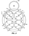
- Fig. 5 illustrates in cross section the structure of Fig. 2 taken along lines 5-5.
- Fig. 6 illustrates in cross section the structure of Fig. 2 taken along lines 6-6.
- Fig. 7 illustrates the portion of the structure of Fig. 5 indicated by lines 7-7.
- Fig. 8 illustrates a portion of the structure of Fig. 1B and 2 comprising a set of mandrels for holding substrates, an end plate connected to one end of the mandrels, and a cruciform connected to the other end of the mandrels.
- Fig. 9 illustrates in plan view an end plate for connecting to the mandrels.
- Fig. 10 illustrates a mandrel used in the apparatus of the above-mentioned figures for holding substrates during plating.
- Figs. 1A and 1B illustrate apparatus 10 for plating a layer of material onto substrates S (Figs. 1B, 2 and 8).
- Substrates S can be disk-shaped metal substrates (e.g. an aluminum or copper alloy), and the material plated onto the substrate can be a nickel-phosphorus alloy. However, these materials are merely exemplary.
- substrates S have a centrally defined opening therein (not shown), but in other embodiments, substrates S do not have such a centrally defined opening.
- Apparatus 10 includes a bath B containing plating solution and a holder 16 immersed in bath B for holding and moving substrates S. (Only one substrate S is shown in Fig. 1B, but typically numerous substrates are simultaneously held by holder 16. The internal structure of holder 16 is not shown in Fig. 1A for ease of illustration, but is shown in Fig. 1B.)
- Apparatus 10 comprises a motor 18 which turns a system of gears GL1-GL3 and GLa-GLd for moving mandrels M (and hence substrates S) in a planetary manner during plating.
- Gears GL1-GL3 and GLa-GLd drive mandrels M from the left side of apparatus 10.
- Gears GR2 and GR3 (similar to gears GL2 and GL3 and shown in Figs. 2 and 5) drive mandrels M from the right side of apparatus 10.
- the motion of substrates S through the plating solution facilitates a) more even plating of material onto the substrate surfaces, b) a more homogenous thickness and surface roughness, and c) greater plating solution velocity across substrates S to remove bubbles and particles to theoretically reduce the number of defects.
- apparatus 10 applies a voltage to substrates S during at least a portion of the plating process via a source of electrical power P, cable 20, bar 22 (mounted on the outside of left wall WL of holder 16), wire 24 (Fig. 2 and 6), spring-loaded contact pin 26, metal contact plate 27 (mounted on gear GL3, and shown in Figs. 2, 4 and 6), a set of trunions TLa-TLd, cruciforms Ca-Cd and mandrels M.
- a "strike voltage" can be applied to substrates S at the start of plating.
- the electrical return path is provided via cables 28 and bars 29 (immersed in bath B, shown in Fig. 1).
- the strike voltage electrical path is discussed below, following the discussion of the mechanism for driving (moving) the mandrels.
- Holder 16 comprises four sets of mandrels M, each set comprising four mandrels for holding a set of substrates S.
- Fig. 1B one set of mandrels (comprising mandrels Ma1, Ma2, Ma3 and Ma4) is shown holding a substrate S.
- the left end of each set of mandrels is connected to an associated one of cruciforms Ca-Cd and on the right end of each set of mandrels is connected to an associated one of end plates Ea-Ed.
- end plates Ea-Ed Only two end plates Ea and Ec, two cruciforms Ca and Cc, and four mandrels M are shown in Fig. 2 because it is a cross section drawing. However, all four end plates Ea-Ed are shown in Fig. 5.
- Each cruciform Ca-Cd is rigidly connected associated posts PLa-PLd, which in turn are rigidly connected to associated gears GLa-GLd.
- Posts PLa-PLd are also rotatably coupled to gear GL3 via trunions TRa-TRd.
- Each end plate Ea-Ed is rotatably coupled via an associated one of posts PRa-PRd to gear GR3.
- gears GLa-GLd, GL3 and GR3 are parts of a gear mechanism that moves mandrels M in a planetary manner during plating. The motion of gear GL3 is synchronized with gear GR3 to cause mandrels M to revolve about the central axis A3 (Fig.
- gear GL3 (which is also the central axis of gear GR3).
- Gear GL3 drives mandrels M from the left side of holder 16, while gear GR3 drives mandrels M from the right side of holder 16.
- a description of the mechanism that drives mandrels M from the left side will be provided, followed by a description of the mechanism that drives mandrels M from the right side.
- a motor 18 drives a rotor shaft 19 which in turn drives first gear GL1 in a direction DL1 (Fig. 3), which in turn drives second gear GL2, in a direction DL2 which in turn drives third gear GL3 in a direction DL3.
- Trunions TLa-TLd are affixed to and extend through associated openings in gear GL3.
- Each one of posts PLa-PLd is rotatably mounted within an associated one of trunions TLa-TLd.
- posts PLa-PLd also rotate about axis A3. Since posts PLa-PLd are rigidly connected to cruciforms Ca-Cd, respectively, cruciforms Ca-Cd and mandrels M also rotate about axis A3.
- a gear GL4 is rigidly (non-rotatably) mounted to wall WR of holder 16.
- Gears GLa-GLd are each rigidly (non-rotatably) connected to an associated one of posts PLa-PLd.
- gear GLa engages gear GL4, thereby causing gear GLa rotate in a direction Da, which in turn causes post PLa, cruciform Ca and the associated set of mandrels Ma1-Ma4 to rotate about the central axis of gear GLa.
- mandrels Ma1-Ma4 rotate about central axis A3 of gear GL3, but they also rotate about the central axis of gear GLa.
- Gears GLb-GLd similarly engage with gear GL3, thereby causing posts PLb-d, cruciforms Cb-d, and their associated mandrels M to rotate about the central axis of associated gears GLb-GLd in directions Db-Dd, respectively.
- gear GL2 also drives an idler shaft 30, which in turn drives gear GR2, which in turn drives gear GR3.
- Gear GR3 is rigidly affixed to a rotating plate 40 (Figs. 5 and 7) via a post 41.
- Posts PRa-PRd extending from associated end plates Ea-Ed, ride in openings Oa-Od of plate 40.
- plate 40 and end plates E also rotate about axis A3.
- Gears GL3 and GR3 move synchronously, and therefore, both sides of mandrels M are driven synchronously.
- Posts PRa-PRd rotate freely within openings Oa-Od. There is nothing analogous to gears GLa-GLd on the right side of holder 16. Thus, in the illustrated embodiment, rotation of mandrels M about the axes of gears GLa-GLd is imparted only from the left side of holder 16 and not from the right side of holder 16. However, in alternative embodiments, such rotation of mandrels M about the axis of gears GLa-GLd can be imparted from both the left and right sides of holder 16. Alternatively, in other embodiments, such motion could be imparted from only the right side of holder 16. Referring to Fig. 5, a ring R extends about plate 40.
- Ring R is fixedly mounted to a side wall WR of holder 16 via posts 48, and does not rotate. Thus, plate 40 rotates within ring R. Ring R prevents posts PRa-PRd from disengaging from openings Oa-Od in plate 40 during use.
- a strike voltage is provided by electrical power source P, cable 20, bar 22, wire 24, spring-loaded contact pin 26, and metal contact plate 27 (mounted on gear GL3, and shown in Figs. 4 and 6).
- Metal contact plate 27 is electrically coupled to mandrels M via trunions TRa-d, posts PLa-d, and cruciforms Ca-d. (Trunions TRa-d, posts PLa-d and cruciforms Ca-d are electrically conductive and typically made of metal.)
- Mandrels M typically comprise an electrically conductive stainless steel core MCO (Fig. 10) surrounded by an electrically insulating polyvinyl difluoride coating MI. As each set of mandrels M is affixed to an associated one of metal cruciforms Ca-d, the conductive core MCO of each mandrel M electrically contacts one of cruciforms Ca-d. As seen in Figs. 8 and 10, each mandrel M comprises a set of notches MN for holding substrates S. Notches MN expose conductive core MCO, so that each substrate S electrically contacts core MCO of the mandrels M holding that substrate. In this way, there is an electrical path from power source P to substrates S.
- Apparatus 10 applies electrical power to substrates S only via the left side of mandrels M.
- end plates E are typically not electrically conductive.
- the various gears in apparatus 10 are also not typically electrically conductive.
- electrical power can be applied to the right side, or both the right and left side, of mandrels M.
- One advantage of using cruciforms Ca-Cd in lieu of conductive plates is the minimization of metallic surface area exposed to the plating solution.
- the shape of electrically conductive plate 27 is also designed to minimize the metallic surface area exposed to the plating solution.
- insulting coating MI also minimizes the metallic surface area exposed to the plating solution.
- each rack typically holds 42 substrates S.
- Holder 16 is designed so that the racks can be removed therefrom.
- an arcuate section Ra of ring R is removed from ring R by removing screws 50a, 50b (Fig. 7).
- apparatus of the present invention can be used for a variety of plating processes, including electroless plating and electroplating.
- an alkaline cleaner e.g. a KOH solution plus an inhibitor
- an acidic solution e.g. phosphoric acid
- This bath comprises the chemicals used to plate NiP, e.g. nickel sulfates, sodium hypophosphite and chelating agents.
- the nickel plating chemistry can be type 300 ADP, manufactured by Enthone Corp.
- a strike voltage of about 3 volts can be applied to the substrates, e.g. for about 15 to 60 seconds, but these parameters are merely exemplary. Thereafter, the substrates can be electrolessly plated in the same bath or a different bath from that used to apply the strike voltage.
- the disclosed apparatus can be used to plate materials other than NiP onto one or more substrates, and the substrates can comprise a material other than Al alloys or spinodal copper.
- the apparatus can be used to apply a strike voltage to initiate electroless plating.
- the apparatus can be used to apply a voltage during electroplating.
- one electrical contact pin 26 multiple pins could be used.
- a brush, strip or ribbon contact could be used.
- gear GL3 is mounted on and rotates about an electrically conductive bearing coupled by an electrically conductive post and bolt to wall WL of holding structure 16.
- wire 24 is connected to the portion of that bolt on the right side of wall WR.
- the conductive bearing is electrically connected to plate 27.
- gears in the drawings have been illustrated as having different thicknesses. In alternative embodiments of the invention, the various gears have the same thickness.
- the mandrels can have the shape of arcuate sections of a cylinder.
- the term mandrel is not limited to a cylindrical mandrel.
- the term "arms" includes mandrels.
- Different numbers of mandrels can be used in each rack of substrates, and holder 16 can be designed to accommodate different numbers of racks (other than four). It is not necessary that all of mandrels M be electrically conductive. Also, it is not necessary that the entirety of cruciforms C be electrically conductive.
- bar 22 and wire 24 can be connected directly to pin 26.
- bars 29 can be arranged at different locations within bath B.
- gear GL3 is replaced with a wheel, and a pulley can connect rotor 19 to the wheel to rotate the mandrels.
- the apparatus can be used to provide a plated layer of materials other than NiP.
- a method and apparatus in accordance with the invention can be used to make masters or stampers, e.g. as discussed in the above-incorporated '380 application.
Landscapes
- Chemical & Material Sciences (AREA)
- Engineering & Computer Science (AREA)
- Chemical Kinetics & Catalysis (AREA)
- Electrochemistry (AREA)
- Materials Engineering (AREA)
- Metallurgy (AREA)
- Organic Chemistry (AREA)
- Electroplating Methods And Accessories (AREA)
- Chemically Coating (AREA)
Applications Claiming Priority (2)
| Application Number | Priority Date | Filing Date | Title |
|---|---|---|---|
| US853953 | 2004-05-26 | ||
| US10/853,953 US7498062B2 (en) | 2004-05-26 | 2004-05-26 | Method and apparatus for applying a voltage to a substrate during plating |
Publications (2)
| Publication Number | Publication Date |
|---|---|
| EP1600529A2 true EP1600529A2 (fr) | 2005-11-30 |
| EP1600529A3 EP1600529A3 (fr) | 2011-01-12 |
Family
ID=34936872
Family Applications (1)
| Application Number | Title | Priority Date | Filing Date |
|---|---|---|---|
| EP05011220A Withdrawn EP1600529A3 (fr) | 2004-05-26 | 2005-05-24 | Procédé et dispositif pour l'application d'une tension sur un ou plusieurs substrats pendant la déposition |
Country Status (4)
| Country | Link |
|---|---|
| US (3) | US7498062B2 (fr) |
| EP (1) | EP1600529A3 (fr) |
| JP (1) | JP4839017B2 (fr) |
| MY (1) | MY146519A (fr) |
Cited By (5)
| Publication number | Priority date | Publication date | Assignee | Title |
|---|---|---|---|---|
| WO2014138840A1 (fr) * | 2013-03-14 | 2014-09-18 | Bradley Wright | Ensemble d'électrodéposition et composants associés |
| CN104894629A (zh) * | 2015-06-26 | 2015-09-09 | 张家口时代橡胶制品股份有限公司 | 磷化生产线工件挂具 |
| US20160024682A1 (en) * | 2011-09-22 | 2016-01-28 | Bradley Wright | Electroplating Assembly And Related Components |
| EP3178970A1 (fr) * | 2015-12-08 | 2017-06-14 | Schaeffler Technologies GmbH & Co. KG | Bati de reception de composants annulaires et procede |
| IT201800010055A1 (it) * | 2018-11-06 | 2020-05-06 | Stefano Zini | Attrezzatura per trattamenti di rivestimento elettrolitico. |
Families Citing this family (93)
| Publication number | Priority date | Publication date | Assignee | Title |
|---|---|---|---|---|
| US7498062B2 (en) * | 2004-05-26 | 2009-03-03 | Wd Media, Inc. | Method and apparatus for applying a voltage to a substrate during plating |
| US7776189B2 (en) * | 2006-03-07 | 2010-08-17 | Abbott Laboratories | Method and apparatus for electropolishing metallic stents |
| JP5117895B2 (ja) | 2008-03-17 | 2013-01-16 | ダブリュディ・メディア・シンガポール・プライベートリミテッド | 磁気記録媒体及びその製造方法 |
| JP2009238299A (ja) | 2008-03-26 | 2009-10-15 | Hoya Corp | 垂直磁気記録媒体および垂直磁気記録媒体の製造方法 |
| JP5453666B2 (ja) * | 2008-03-30 | 2014-03-26 | ダブリュディ・メディア・シンガポール・プライベートリミテッド | 磁気ディスク及びその製造方法 |
| JP2011034603A (ja) * | 2008-03-31 | 2011-02-17 | Hoya Corp | 垂直磁気記録媒体 |
| US8323459B2 (en) * | 2008-04-10 | 2012-12-04 | Abbott Cardiovascular Systems Inc. | Automated electropolishing process |
| US9177586B2 (en) | 2008-09-30 | 2015-11-03 | WD Media (Singapore), LLC | Magnetic disk and manufacturing method thereof |
| WO2010064724A1 (fr) | 2008-12-05 | 2010-06-10 | Hoya株式会社 | Disque magnétique et procédé de fabrication associé |
| US20100175619A1 (en) * | 2009-01-15 | 2010-07-15 | Joseph Garfield Albanese | Part mounting apparatus |
| WO2010116908A1 (fr) | 2009-03-28 | 2010-10-14 | Hoya株式会社 | Composé lubrifiant pour disque magnétique et disque magnétique |
| US8431258B2 (en) | 2009-03-30 | 2013-04-30 | Wd Media (Singapore) Pte. Ltd. | Perpendicular magnetic recording medium and method of manufacturing the same |
| US8267831B1 (en) | 2009-05-19 | 2012-09-18 | Western Digital Technologies, Inc. | Method and apparatus for washing, etching, rinsing, and plating substrates |
| US20100300884A1 (en) | 2009-05-26 | 2010-12-02 | Wd Media, Inc. | Electro-deposited passivation coatings for patterned media |
| US8596214B2 (en) * | 2009-09-29 | 2013-12-03 | Larry J. Schieszer | Wood grilling plank soaking device |
| US9330685B1 (en) | 2009-11-06 | 2016-05-03 | WD Media, LLC | Press system for nano-imprinting of recording media with a two step pressing method |
| US8496466B1 (en) | 2009-11-06 | 2013-07-30 | WD Media, LLC | Press system with interleaved embossing foil holders for nano-imprinting of recording media |
| JP5643516B2 (ja) | 2010-01-08 | 2014-12-17 | ダブリュディ・メディア・シンガポール・プライベートリミテッド | 垂直磁気記録媒体 |
| JP5574414B2 (ja) | 2010-03-29 | 2014-08-20 | ダブリュディ・メディア・シンガポール・プライベートリミテッド | 磁気ディスクの評価方法及び磁気ディスクの製造方法 |
| US8658006B2 (en) | 2010-04-12 | 2014-02-25 | Abbott Cardiovascular Systems Inc. | System and method for electropolising devices |
| JP5645476B2 (ja) | 2010-05-21 | 2014-12-24 | ダブリュディ・メディア・シンガポール・プライベートリミテッド | 垂直磁気ディスク |
| JP5634749B2 (ja) | 2010-05-21 | 2014-12-03 | ダブリュディ・メディア・シンガポール・プライベートリミテッド | 垂直磁気ディスク |
| JP2011248968A (ja) | 2010-05-28 | 2011-12-08 | Wd Media (Singapore) Pte. Ltd | 垂直磁気ディスク |
| US9456508B2 (en) * | 2010-05-28 | 2016-09-27 | Apple Inc. | Methods for assembling electronic devices by internally curing light-sensitive adhesive |
| JP2011248967A (ja) | 2010-05-28 | 2011-12-08 | Wd Media (Singapore) Pte. Ltd | 垂直磁気ディスクの製造方法 |
| JP2011248969A (ja) | 2010-05-28 | 2011-12-08 | Wd Media (Singapore) Pte. Ltd | 垂直磁気ディスク |
| JP2012009086A (ja) | 2010-06-22 | 2012-01-12 | Wd Media (Singapore) Pte. Ltd | 垂直磁気記録媒体及びその製造方法 |
| US8889275B1 (en) | 2010-08-20 | 2014-11-18 | WD Media, LLC | Single layer small grain size FePT:C film for heat assisted magnetic recording media |
| US9222191B2 (en) | 2010-10-20 | 2015-12-29 | Seagate Technology Llc | Laminar flow plating rack |
| US11298251B2 (en) | 2010-11-17 | 2022-04-12 | Abbott Cardiovascular Systems, Inc. | Radiopaque intraluminal stents comprising cobalt-based alloys with primarily single-phase supersaturated tungsten content |
| US8743666B1 (en) | 2011-03-08 | 2014-06-03 | Western Digital Technologies, Inc. | Energy assisted magnetic recording medium capable of suppressing high DC readback noise |
| US8711499B1 (en) | 2011-03-10 | 2014-04-29 | WD Media, LLC | Methods for measuring media performance associated with adjacent track interference |
| US8491800B1 (en) | 2011-03-25 | 2013-07-23 | WD Media, LLC | Manufacturing of hard masks for patterning magnetic media |
| US9028985B2 (en) | 2011-03-31 | 2015-05-12 | WD Media, LLC | Recording media with multiple exchange coupled magnetic layers |
| US9724494B2 (en) | 2011-06-29 | 2017-08-08 | Abbott Cardiovascular Systems, Inc. | Guide wire device including a solderable linear elastic nickel-titanium distal end section and methods of preparation therefor |
| TWI485286B (zh) * | 2011-11-16 | 2015-05-21 | 荏原製作所股份有限公司 | Electroless plating and electroless plating |
| US9266310B2 (en) | 2011-12-16 | 2016-02-23 | Apple Inc. | Methods of joining device structures with adhesive |
| US8565050B1 (en) | 2011-12-20 | 2013-10-22 | WD Media, LLC | Heat assisted magnetic recording media having moment keeper layer |
| US9029308B1 (en) | 2012-03-28 | 2015-05-12 | WD Media, LLC | Low foam media cleaning detergent |
| US9269480B1 (en) | 2012-03-30 | 2016-02-23 | WD Media, LLC | Systems and methods for forming magnetic recording media with improved grain columnar growth for energy assisted magnetic recording |
| US8941950B2 (en) | 2012-05-23 | 2015-01-27 | WD Media, LLC | Underlayers for heat assisted magnetic recording (HAMR) media |
| US8993134B2 (en) | 2012-06-29 | 2015-03-31 | Western Digital Technologies, Inc. | Electrically conductive underlayer to grow FePt granular media with (001) texture on glass substrates |
| US9034492B1 (en) | 2013-01-11 | 2015-05-19 | WD Media, LLC | Systems and methods for controlling damping of magnetic media for heat assisted magnetic recording |
| US10115428B1 (en) | 2013-02-15 | 2018-10-30 | Wd Media, Inc. | HAMR media structure having an anisotropic thermal barrier layer |
| US9153268B1 (en) | 2013-02-19 | 2015-10-06 | WD Media, LLC | Lubricants comprising fluorinated graphene nanoribbons for magnetic recording media structure |
| US9183867B1 (en) | 2013-02-21 | 2015-11-10 | WD Media, LLC | Systems and methods for forming implanted capping layers in magnetic media for magnetic recording |
| US9196283B1 (en) | 2013-03-13 | 2015-11-24 | Western Digital (Fremont), Llc | Method for providing a magnetic recording transducer using a chemical buffer |
| US9190094B2 (en) | 2013-04-04 | 2015-11-17 | Western Digital (Fremont) | Perpendicular recording media with grain isolation initiation layer and exchange breaking layer for signal-to-noise ratio enhancement |
| US9093122B1 (en) | 2013-04-05 | 2015-07-28 | WD Media, LLC | Systems and methods for improving accuracy of test measurements involving aggressor tracks written to disks of hard disk drives |
| US8947987B1 (en) | 2013-05-03 | 2015-02-03 | WD Media, LLC | Systems and methods for providing capping layers for heat assisted magnetic recording media |
| US8867322B1 (en) | 2013-05-07 | 2014-10-21 | WD Media, LLC | Systems and methods for providing thermal barrier bilayers for heat assisted magnetic recording media |
| US9296082B1 (en) | 2013-06-11 | 2016-03-29 | WD Media, LLC | Disk buffing apparatus with abrasive tape loading pad having a vibration absorbing layer |
| US9406330B1 (en) | 2013-06-19 | 2016-08-02 | WD Media, LLC | Method for HDD disk defect source detection |
| US9607646B2 (en) | 2013-07-30 | 2017-03-28 | WD Media, LLC | Hard disk double lubrication layer |
| US9389135B2 (en) | 2013-09-26 | 2016-07-12 | WD Media, LLC | Systems and methods for calibrating a load cell of a disk burnishing machine |
| US9177585B1 (en) | 2013-10-23 | 2015-11-03 | WD Media, LLC | Magnetic media capable of improving magnetic properties and thermal management for heat-assisted magnetic recording |
| US9581510B1 (en) | 2013-12-16 | 2017-02-28 | Western Digital Technologies, Inc. | Sputter chamber pressure gauge with vibration absorber |
| US9382496B1 (en) | 2013-12-19 | 2016-07-05 | Western Digital Technologies, Inc. | Lubricants with high thermal stability for heat-assisted magnetic recording |
| US9824711B1 (en) | 2014-02-14 | 2017-11-21 | WD Media, LLC | Soft underlayer for heat assisted magnetic recording media |
| US9447368B1 (en) | 2014-02-18 | 2016-09-20 | WD Media, LLC | Detergent composition with low foam and high nickel solubility |
| US9431045B1 (en) | 2014-04-25 | 2016-08-30 | WD Media, LLC | Magnetic seed layer used with an unbalanced soft underlayer |
| US9042053B1 (en) | 2014-06-24 | 2015-05-26 | WD Media, LLC | Thermally stabilized perpendicular magnetic recording medium |
| US9159350B1 (en) | 2014-07-02 | 2015-10-13 | WD Media, LLC | High damping cap layer for magnetic recording media |
| US10054363B2 (en) | 2014-08-15 | 2018-08-21 | WD Media, LLC | Method and apparatus for cryogenic dynamic cooling |
| US9082447B1 (en) | 2014-09-22 | 2015-07-14 | WD Media, LLC | Determining storage media substrate material type |
| US9227324B1 (en) | 2014-09-25 | 2016-01-05 | WD Media, LLC | Mandrel for substrate transport system with notch |
| US8995078B1 (en) | 2014-09-25 | 2015-03-31 | WD Media, LLC | Method of testing a head for contamination |
| US9685184B1 (en) | 2014-09-25 | 2017-06-20 | WD Media, LLC | NiFeX-based seed layer for magnetic recording media |
| US9449633B1 (en) | 2014-11-06 | 2016-09-20 | WD Media, LLC | Smooth structures for heat-assisted magnetic recording media |
| US9818442B2 (en) | 2014-12-01 | 2017-11-14 | WD Media, LLC | Magnetic media having improved magnetic grain size distribution and intergranular segregation |
| US9401300B1 (en) | 2014-12-18 | 2016-07-26 | WD Media, LLC | Media substrate gripper including a plurality of snap-fit fingers |
| US9218850B1 (en) | 2014-12-23 | 2015-12-22 | WD Media, LLC | Exchange break layer for heat-assisted magnetic recording media |
| US9257134B1 (en) | 2014-12-24 | 2016-02-09 | Western Digital Technologies, Inc. | Allowing fast data zone switches on data storage devices |
| US9990940B1 (en) | 2014-12-30 | 2018-06-05 | WD Media, LLC | Seed structure for perpendicular magnetic recording media |
| CN104611758B (zh) * | 2015-01-30 | 2017-05-10 | 广东保迪环保电镀设备有限公司 | 一种行星式滚镀机 |
| US9280998B1 (en) | 2015-03-30 | 2016-03-08 | WD Media, LLC | Acidic post-sputter wash for magnetic recording media |
| US9822441B2 (en) | 2015-03-31 | 2017-11-21 | WD Media, LLC | Iridium underlayer for heat assisted magnetic recording media |
| US9275669B1 (en) | 2015-03-31 | 2016-03-01 | WD Media, LLC | TbFeCo in PMR media for SNR improvement |
| CN105133000B (zh) * | 2015-08-27 | 2018-06-22 | 深圳市佳易研磨有限公司 | 卧式旋转挂具装置 |
| US11074934B1 (en) | 2015-09-25 | 2021-07-27 | Western Digital Technologies, Inc. | Heat assisted magnetic recording (HAMR) media with Curie temperature reduction layer |
| US10236026B1 (en) | 2015-11-06 | 2019-03-19 | WD Media, LLC | Thermal barrier layers and seed layers for control of thermal and structural properties of HAMR media |
| US9406329B1 (en) | 2015-11-30 | 2016-08-02 | WD Media, LLC | HAMR media structure with intermediate layer underlying a magnetic recording layer having multiple sublayers |
| US10121506B1 (en) | 2015-12-29 | 2018-11-06 | WD Media, LLC | Magnetic-recording medium including a carbon overcoat implanted with nitrogen and hydrogen |
| WO2018118075A1 (fr) | 2016-12-23 | 2018-06-28 | Intel Corporation | Procédés et systèmes de carte sonde à pas fin |
| US11268983B2 (en) | 2017-06-30 | 2022-03-08 | Intel Corporation | Chevron interconnect for very fine pitch probing |
| US10775414B2 (en) | 2017-09-29 | 2020-09-15 | Intel Corporation | Low-profile gimbal platform for high-resolution in situ co-planarity adjustment |
| US11061068B2 (en) | 2017-12-05 | 2021-07-13 | Intel Corporation | Multi-member test probe structure |
| US11204555B2 (en) * | 2017-12-28 | 2021-12-21 | Intel Corporation | Method and apparatus to develop lithographically defined high aspect ratio interconnects |
| US11073538B2 (en) | 2018-01-03 | 2021-07-27 | Intel Corporation | Electrical testing apparatus with lateral movement of a probe support substrate |
| US10488438B2 (en) | 2018-01-05 | 2019-11-26 | Intel Corporation | High density and fine pitch interconnect structures in an electric test apparatus |
| US11543454B2 (en) | 2018-09-25 | 2023-01-03 | Intel Corporation | Double-beam test probe |
| US10935573B2 (en) | 2018-09-28 | 2021-03-02 | Intel Corporation | Slip-plane MEMS probe for high-density and fine pitch interconnects |
| US12151049B2 (en) | 2019-10-14 | 2024-11-26 | Abbott Cardiovascular Systems, Inc. | Methods for manufacturing radiopaque intraluminal stents comprising cobalt-based alloys with supersaturated tungsten content |
Family Cites Families (67)
| Publication number | Priority date | Publication date | Assignee | Title |
|---|---|---|---|---|
| US655972A (en) * | 1899-12-09 | 1900-08-14 | Reinhold Hakewessell | Clutch. |
| US1475937A (en) | 1919-09-30 | 1923-12-04 | Hanson & Van Winkle Co | Phonograph-record matrix and method and apparatus for producing same |
| US1453419A (en) | 1921-09-12 | 1923-05-01 | Wm A Rogers Ltd | Electroplating apparatus |
| US2244197A (en) | 1936-03-25 | 1941-06-03 | Hessler Christian Rudolph | Bearing |
| US2211295A (en) | 1938-04-09 | 1940-08-13 | Fafnir Bearing Co | Bearing device |
| US2979452A (en) | 1954-08-23 | 1961-04-11 | Nat Forge Co | Apparatus for electroplating crankshaft journals |
| US3137246A (en) * | 1962-03-05 | 1964-06-16 | Huss Equipment Corp | Carrier fixtures |
| US3304138A (en) | 1964-08-14 | 1967-02-14 | Gen Motors Corp | Antifriction bearing |
| US3607712A (en) * | 1969-01-21 | 1971-09-21 | Ionic International Inc | Barrel-type processing apparatus |
| US3640592A (en) | 1969-10-23 | 1972-02-08 | Textron Inc | Antifriction bearing with embedded race inserts |
| US3880480A (en) | 1971-07-06 | 1975-04-29 | Trw Inc | Nonmetallic bearing housing |
| US4105310A (en) * | 1975-12-24 | 1978-08-08 | Minolta Camera Kabushiki Kaisha | Indicating device for motion picture camera |
| JPS585107B2 (ja) * | 1978-12-27 | 1983-01-29 | ワイケイケイ株式会社 | 小物品の塗装装置 |
| CH627826A5 (fr) | 1978-12-31 | 1982-01-29 | Schmid Roost J Sro Kugellagerw | Element de guidage axial-rotatif. |
| US4305804A (en) * | 1980-05-07 | 1981-12-15 | Harshaw Chemical Company | Plating barrel contact |
| US4324441A (en) | 1980-10-24 | 1982-04-13 | Rouverol William S | Rolling contact element |
| US4516523A (en) | 1983-12-16 | 1985-05-14 | Knox David J | Apparatus for wetting apertured discs |
| US4581260A (en) | 1984-09-25 | 1986-04-08 | Ampex Corporation | Electroless plating method and apparatus |
| JPS61133380A (ja) * | 1984-12-03 | 1986-06-20 | Katsukawa Kogyo Kk | 化学表面処理方法 |
| JPS61200874A (ja) * | 1985-02-28 | 1986-09-05 | Mitsui Kinzoku Eng Kk | 鋼製小物類の表面処理装置 |
| JPH0627352B2 (ja) * | 1985-08-06 | 1994-04-13 | 日本電気株式会社 | 表面処理装置用カ−ロセル |
| US4855020A (en) * | 1985-12-06 | 1989-08-08 | Microsurface Technology Corp. | Apparatus and method for the electrolytic plating of layers onto computer memory hard discs |
| JPS62183036A (ja) * | 1986-02-06 | 1987-08-11 | Chuo Seisakusho:Kk | 磁気デイスク基板のめつき装置 |
| JPH01275771A (ja) * | 1988-04-28 | 1989-11-06 | Brother Ind Ltd | 無電解メッキ装置及び該無電解メッキ装置を用いた無電解メッキ方法 |
| US5176456A (en) * | 1989-05-01 | 1993-01-05 | Koyo Seiko Co., Ltd. | Rolling bearing |
| US4951763A (en) * | 1989-11-13 | 1990-08-28 | Hi-Speed Checkweigher Co., Inc. | Checkweigher |
| US5275184A (en) * | 1990-10-19 | 1994-01-04 | Dainippon Screen Mfg. Co., Ltd. | Apparatus and system for treating surface of a wafer by dipping the same in a treatment solution and a gate device for chemical agent used in the apparatus and the system |
| US5174045A (en) | 1991-05-17 | 1992-12-29 | Semitool, Inc. | Semiconductor processor with extendible receiver for handling multiple discrete wafers without wafer carriers |
| DE4209732A1 (de) * | 1992-03-25 | 1993-09-30 | Schloetter Ges Mbh Salzburg | Vorrichtung zum Aufbringen galvanischer Überzüge auf metallische Gegenstände |
| US5264256A (en) | 1992-09-08 | 1993-11-23 | Xerox Corporation | Apparatus and process for glow discharge comprising substrate temperature control by shutter adjustment |
| US5358460A (en) * | 1993-01-25 | 1994-10-25 | The United States Of America As Represented By The Administrator Of The National Aeronautics And Space Administration | Flex-gear power transmission system for transmitting EMF between sun and ring gears |
| JP2877217B2 (ja) * | 1993-03-29 | 1999-03-31 | 日本軽金属株式会社 | 表面処理装置 |
| JP2877218B2 (ja) * | 1993-03-29 | 1999-03-31 | 日本軽金属株式会社 | 表面処理装置 |
| US5750207A (en) | 1995-02-17 | 1998-05-12 | Si Diamond Technology, Inc. | System and method for depositing coating of modulated composition |
| AU5177496A (en) * | 1995-03-06 | 1996-09-23 | Intel Corporation | A computer system with unattended on-demand availability |
| TW325588B (en) | 1996-02-28 | 1998-01-21 | Asahi Glass Co Ltd | Vertical wafer boat |
| US6358388B1 (en) | 1996-07-15 | 2002-03-19 | Semitool, Inc. | Plating system workpiece support having workpiece-engaging electrodes with distal contact-part and dielectric cover |
| JP3176294B2 (ja) | 1996-08-26 | 2001-06-11 | 日本電気株式会社 | 半導体ウェーハ用キャリア |
| US5716147A (en) | 1997-02-07 | 1998-02-10 | Emerson Power Transmission Corp. | Corrosion-resistant bearing assembly |
| US6372303B1 (en) | 1997-06-16 | 2002-04-16 | Robert Bosch Gmbh | Method and device for vacuum-coating a substrate |
| USD411176S (en) | 1997-08-20 | 1999-06-22 | Tokyo Electron Limited | Wafer boat for use in a semiconductor wafer heat processing apparatus |
| US6056123A (en) | 1997-12-10 | 2000-05-02 | Novus Corporation | Semiconductor wafer carrier having the same composition as the wafers |
| US5951763A (en) * | 1998-02-09 | 1999-09-14 | Knox; David J. | Immersible rotatable carousel apparatus for wetting articles of manufacture |
| US5997947A (en) | 1998-04-29 | 1999-12-07 | United Technologies Corporation | Rotisserie fixture for coating airfoils |
| US6099702A (en) * | 1998-06-10 | 2000-08-08 | Novellus Systems, Inc. | Electroplating chamber with rotatable wafer holder and pre-wetting and rinsing capability |
| KR20000002833A (ko) | 1998-06-23 | 2000-01-15 | 윤종용 | 반도체 웨이퍼 보트 |
| US6216709B1 (en) | 1998-09-04 | 2001-04-17 | Komag, Inc. | Method for drying a substrate |
| US6225594B1 (en) | 1999-04-15 | 2001-05-01 | Integrated Materials, Inc. | Method and apparatus for securing components of wafer processing fixtures |
| JP2000345356A (ja) * | 1999-06-04 | 2000-12-12 | Mitsubishi Materials Corp | ディスク基板のめっき処理装置 |
| JP2001003177A (ja) * | 1999-06-18 | 2001-01-09 | Mitsubishi Materials Corp | ディスク基板のめっき処理装置 |
| US6673216B2 (en) | 1999-08-31 | 2004-01-06 | Semitool, Inc. | Apparatus for providing electrical and fluid communication to a rotating microelectronic workpiece during electrochemical processing |
| DE19948423B4 (de) | 1999-10-07 | 2006-11-30 | Ina-Schaeffler Kg | Transport- und Montagevorrichtung für Wälzkörpersätze |
| JP2001181893A (ja) * | 1999-10-13 | 2001-07-03 | Sumitomo Special Metals Co Ltd | 表面処理装置 |
| JP3698403B2 (ja) | 2000-02-28 | 2005-09-21 | 東京エレクトロン株式会社 | 回転式液処理装置 |
| US6370791B1 (en) | 2000-03-10 | 2002-04-16 | Semitool, Inc. | Processing machine with lockdown rotor |
| US6852208B2 (en) * | 2000-03-17 | 2005-02-08 | Nutool, Inc. | Method and apparatus for full surface electrotreating of a wafer |
| EP1139396A3 (fr) * | 2000-03-31 | 2003-08-27 | Texas Instruments Incorporated | Dispositif de fixation et procédé pour dépôt sans courant uniforme d'un métal sur des plots d'interconnexion de circuit intégré |
| US6341935B1 (en) | 2000-06-14 | 2002-01-29 | Taiwan Semiconductor Manufacturing Company, Ltd. | Wafer boat having improved wafer holding capability |
| US6709563B2 (en) | 2000-06-30 | 2004-03-23 | Ebara Corporation | Copper-plating liquid, plating method and plating apparatus |
| US6418945B1 (en) | 2000-07-07 | 2002-07-16 | Semitool, Inc. | Dual cassette centrifugal processor |
| JP2002038275A (ja) * | 2000-07-25 | 2002-02-06 | Mitsubishi Materials Corp | 円板支持具 |
| US6528124B1 (en) | 2000-12-01 | 2003-03-04 | Komag, Inc. | Disk carrier |
| US6558750B2 (en) | 2001-07-16 | 2003-05-06 | Technic Inc. | Method of processing and plating planar articles |
| US6664122B1 (en) | 2001-10-19 | 2003-12-16 | Novellus Systems, Inc. | Electroless copper deposition method for preparing copper seed layers |
| US7067045B2 (en) * | 2002-10-18 | 2006-06-27 | Applied Materials, Inc. | Method and apparatus for sealing electrical contacts during an electrochemical deposition process |
| US20050056542A1 (en) * | 2003-07-04 | 2005-03-17 | Seiko Epson Corporation | Plating tool, plating method, electroplating apparatus, plated product, and method for producing plated product |
| US7498062B2 (en) | 2004-05-26 | 2009-03-03 | Wd Media, Inc. | Method and apparatus for applying a voltage to a substrate during plating |
-
2004
- 2004-05-26 US US10/853,953 patent/US7498062B2/en not_active Expired - Fee Related
-
2005
- 2005-03-23 US US11/088,052 patent/US20050263401A1/en not_active Abandoned
- 2005-05-23 JP JP2005149681A patent/JP4839017B2/ja not_active Expired - Fee Related
- 2005-05-24 EP EP05011220A patent/EP1600529A3/fr not_active Withdrawn
- 2005-05-26 MY MYPI20052384A patent/MY146519A/en unknown
-
2009
- 2009-02-13 US US12/371,397 patent/US7758732B1/en not_active Expired - Fee Related
Cited By (6)
| Publication number | Priority date | Publication date | Assignee | Title |
|---|---|---|---|---|
| US20160024682A1 (en) * | 2011-09-22 | 2016-01-28 | Bradley Wright | Electroplating Assembly And Related Components |
| WO2014138840A1 (fr) * | 2013-03-14 | 2014-09-18 | Bradley Wright | Ensemble d'électrodéposition et composants associés |
| CN104894629A (zh) * | 2015-06-26 | 2015-09-09 | 张家口时代橡胶制品股份有限公司 | 磷化生产线工件挂具 |
| EP3178970A1 (fr) * | 2015-12-08 | 2017-06-14 | Schaeffler Technologies GmbH & Co. KG | Bati de reception de composants annulaires et procede |
| WO2017097300A1 (fr) * | 2015-12-08 | 2017-06-15 | Schaeffler Technologies AG & Co. KG | Châssis pour la réception de pièces annulaires et procédé |
| IT201800010055A1 (it) * | 2018-11-06 | 2020-05-06 | Stefano Zini | Attrezzatura per trattamenti di rivestimento elettrolitico. |
Also Published As
| Publication number | Publication date |
|---|---|
| US20050274605A1 (en) | 2005-12-15 |
| JP4839017B2 (ja) | 2011-12-14 |
| MY146519A (en) | 2012-08-15 |
| US7758732B1 (en) | 2010-07-20 |
| EP1600529A3 (fr) | 2011-01-12 |
| US7498062B2 (en) | 2009-03-03 |
| JP2005336612A (ja) | 2005-12-08 |
| US20050263401A1 (en) | 2005-12-01 |
Similar Documents
| Publication | Publication Date | Title |
|---|---|---|
| US7758732B1 (en) | Method and apparatus for applying a voltage to a substrate during plating | |
| US5141626A (en) | Method of and apparatus for surface treatment for half bearings | |
| CN115555925A (zh) | 振动磁场辅助电化学磁性磨料复合抛光装置及其使用方法 | |
| JPS63282289A (ja) | 電磁波遮蔽用金属格子 | |
| US3259556A (en) | Ribbon electroplating method | |
| JP2015035945A (ja) | スピンドルモータ及びハードディスク装置 | |
| RU2398918C2 (ru) | Установка для обработки поверхностей металлических деталей, в частности, электролизом | |
| CN115532677A (zh) | 一种环保低耗型镀锡导体生产工艺及装置 | |
| JPH0790596A (ja) | 表面処理装置および表面処理方法 | |
| JP2002097591A (ja) | 金属粉末の製造方法 | |
| JP3461060B2 (ja) | バレルメッキ装置 | |
| JPH0452275A (ja) | スパツタリング装置 | |
| CN210270413U (zh) | 一种隐形眼镜脱膜机 | |
| RU2841704C1 (ru) | Устройство для формирования тонкопленочных покрытий наноразмерной толщины методом ионного наслаивания | |
| JPH11100698A (ja) | メッキ装置 | |
| JPH0841649A (ja) | 表面処理装置 | |
| JPH0344479A (ja) | スピナー法による無電解めっき方法及びその装置 | |
| TW491750B (en) | Method and apparatus for electrochemical planarization of a workpiece | |
| CA2028196A1 (fr) | Electroplacage de pieces de precision | |
| KR100833019B1 (ko) | 전기도금공정의 유기 서포트 롤 | |
| JP2938172B2 (ja) | スリップリングの電気めっき装置 | |
| JPH07126884A (ja) | 部分めっきリード線の製造装置 | |
| CN120627617A (zh) | 一种阀芯清洗后的自动干燥及防锈处理一体机 | |
| JPH01177974A (ja) | 電着砥石の製造方法 | |
| JP2003321790A (ja) | 中空金属部材の製造方法および電鋳装置 |
Legal Events
| Date | Code | Title | Description |
|---|---|---|---|
| PUAI | Public reference made under article 153(3) epc to a published international application that has entered the european phase |
Free format text: ORIGINAL CODE: 0009012 |
|
| AK | Designated contracting states |
Kind code of ref document: A2 Designated state(s): AT BE BG CH CY CZ DE DK EE ES FI FR GB GR HU IE IS IT LI LT LU MC NL PL PT RO SE SI SK TR |
|
| AX | Request for extension of the european patent |
Extension state: AL BA HR LV MK YU |
|
| PUAL | Search report despatched |
Free format text: ORIGINAL CODE: 0009013 |
|
| AK | Designated contracting states |
Kind code of ref document: A3 Designated state(s): AT BE BG CH CY CZ DE DK EE ES FI FR GB GR HU IE IS IT LI LT LU MC NL PL PT RO SE SI SK TR |
|
| AX | Request for extension of the european patent |
Extension state: AL BA HR LV MK YU |
|
| 17P | Request for examination filed |
Effective date: 20110624 |
|
| AKX | Designation fees paid |
Designated state(s): AT BE BG CH CY CZ DE DK EE ES FI FR GB GR HU IE IS IT LI LT LU MC NL PL PT RO SE SI SK TR |
|
| 17Q | First examination report despatched |
Effective date: 20130319 |
|
| STAA | Information on the status of an ep patent application or granted ep patent |
Free format text: STATUS: THE APPLICATION IS DEEMED TO BE WITHDRAWN |
|
| 18D | Application deemed to be withdrawn |
Effective date: 20130730 |