EP1596408A2 - Dispositif émetteur d'électrons, source d'électrons et procédé de fabrication d'un dispositif d'affichage d'images - Google Patents
Dispositif émetteur d'électrons, source d'électrons et procédé de fabrication d'un dispositif d'affichage d'images Download PDFInfo
- Publication number
- EP1596408A2 EP1596408A2 EP05008198A EP05008198A EP1596408A2 EP 1596408 A2 EP1596408 A2 EP 1596408A2 EP 05008198 A EP05008198 A EP 05008198A EP 05008198 A EP05008198 A EP 05008198A EP 1596408 A2 EP1596408 A2 EP 1596408A2
- Authority
- EP
- European Patent Office
- Prior art keywords
- electron
- electroconductive members
- substrate
- electroconductive
- emitting device
- Prior art date
- Legal status (The legal status is an assumption and is not a legal conclusion. Google has not performed a legal analysis and makes no representation as to the accuracy of the status listed.)
- Withdrawn
Links
- 238000000034 method Methods 0.000 title claims description 106
- 238000004519 manufacturing process Methods 0.000 title claims description 34
- 239000000758 substrate Substances 0.000 claims abstract description 72
- 238000001803 electron scattering Methods 0.000 claims abstract description 37
- OKTJSMMVPCPJKN-UHFFFAOYSA-N Carbon Chemical compound [C] OKTJSMMVPCPJKN-UHFFFAOYSA-N 0.000 claims description 45
- 229910052799 carbon Inorganic materials 0.000 claims description 40
- 229910052751 metal Inorganic materials 0.000 claims description 27
- 239000002184 metal Substances 0.000 claims description 27
- OAICVXFJPJFONN-UHFFFAOYSA-N Phosphorus Chemical compound [P] OAICVXFJPJFONN-UHFFFAOYSA-N 0.000 claims description 16
- 150000001722 carbon compounds Chemical class 0.000 claims description 15
- 239000012298 atmosphere Substances 0.000 claims description 9
- 150000001875 compounds Chemical class 0.000 claims description 6
- 239000010408 film Substances 0.000 description 113
- 239000010409 thin film Substances 0.000 description 57
- 230000008569 process Effects 0.000 description 53
- 238000012545 processing Methods 0.000 description 52
- 239000000463 material Substances 0.000 description 34
- 238000001994 activation Methods 0.000 description 28
- 230000004913 activation Effects 0.000 description 20
- 239000010410 layer Substances 0.000 description 19
- 230000000052 comparative effect Effects 0.000 description 17
- 238000001704 evaporation Methods 0.000 description 15
- 238000010438 heat treatment Methods 0.000 description 15
- BASFCYQUMIYNBI-UHFFFAOYSA-N platinum Substances [Pt] BASFCYQUMIYNBI-UHFFFAOYSA-N 0.000 description 14
- 230000008020 evaporation Effects 0.000 description 13
- 239000011521 glass Substances 0.000 description 13
- KDLHZDBZIXYQEI-UHFFFAOYSA-N palladium Substances [Pd] KDLHZDBZIXYQEI-UHFFFAOYSA-N 0.000 description 13
- 230000015572 biosynthetic process Effects 0.000 description 12
- 238000009413 insulation Methods 0.000 description 11
- 239000011229 interlayer Substances 0.000 description 11
- 238000005259 measurement Methods 0.000 description 11
- VYPSYNLAJGMNEJ-UHFFFAOYSA-N Silicium dioxide Chemical compound O=[Si]=O VYPSYNLAJGMNEJ-UHFFFAOYSA-N 0.000 description 10
- 238000010894 electron beam technology Methods 0.000 description 9
- 239000011159 matrix material Substances 0.000 description 9
- HBEQXAKJSGXAIQ-UHFFFAOYSA-N oxopalladium Chemical compound [Pd]=O HBEQXAKJSGXAIQ-UHFFFAOYSA-N 0.000 description 9
- 239000000243 solution Substances 0.000 description 9
- 239000007789 gas Substances 0.000 description 8
- 238000004544 sputter deposition Methods 0.000 description 8
- NWPNXBQSRGKSJB-UHFFFAOYSA-N 2-methylbenzonitrile Chemical compound CC1=CC=CC=C1C#N NWPNXBQSRGKSJB-UHFFFAOYSA-N 0.000 description 7
- 229910052763 palladium Inorganic materials 0.000 description 7
- 229910003445 palladium oxide Inorganic materials 0.000 description 7
- 229910052697 platinum Inorganic materials 0.000 description 7
- KFZMGEQAYNKOFK-UHFFFAOYSA-N Isopropanol Chemical compound CC(C)O KFZMGEQAYNKOFK-UHFFFAOYSA-N 0.000 description 6
- 238000000576 coating method Methods 0.000 description 6
- 239000013078 crystal Substances 0.000 description 6
- 238000010586 diagram Methods 0.000 description 6
- 238000011156 evaluation Methods 0.000 description 6
- 230000006641 stabilisation Effects 0.000 description 6
- 238000011105 stabilization Methods 0.000 description 6
- 239000010936 titanium Substances 0.000 description 6
- 238000001771 vacuum deposition Methods 0.000 description 6
- 239000011248 coating agent Substances 0.000 description 5
- 229910052737 gold Inorganic materials 0.000 description 5
- 229910002804 graphite Inorganic materials 0.000 description 5
- 239000010439 graphite Substances 0.000 description 5
- 150000002736 metal compounds Chemical class 0.000 description 5
- 238000007639 printing Methods 0.000 description 5
- ISWSIDIOOBJBQZ-UHFFFAOYSA-N Phenol Chemical compound OC1=CC=CC=C1 ISWSIDIOOBJBQZ-UHFFFAOYSA-N 0.000 description 4
- 238000004833 X-ray photoelectron spectroscopy Methods 0.000 description 4
- 229910052681 coesite Inorganic materials 0.000 description 4
- 239000004020 conductor Substances 0.000 description 4
- 229910052906 cristobalite Inorganic materials 0.000 description 4
- 238000004453 electron probe microanalysis Methods 0.000 description 4
- 239000010419 fine particle Substances 0.000 description 4
- 239000000377 silicon dioxide Substances 0.000 description 4
- 229910052682 stishovite Inorganic materials 0.000 description 4
- 229910052905 tridymite Inorganic materials 0.000 description 4
- ZWEHNKRNPOVVGH-UHFFFAOYSA-N 2-Butanone Chemical compound CCC(C)=O ZWEHNKRNPOVVGH-UHFFFAOYSA-N 0.000 description 3
- QTBSBXVTEAMEQO-UHFFFAOYSA-N Acetic acid Chemical compound CC(O)=O QTBSBXVTEAMEQO-UHFFFAOYSA-N 0.000 description 3
- CSCPPACGZOOCGX-UHFFFAOYSA-N Acetone Chemical compound CC(C)=O CSCPPACGZOOCGX-UHFFFAOYSA-N 0.000 description 3
- UHOVQNZJYSORNB-UHFFFAOYSA-N Benzene Chemical compound C1=CC=CC=C1 UHOVQNZJYSORNB-UHFFFAOYSA-N 0.000 description 3
- LFQSCWFLJHTTHZ-UHFFFAOYSA-N Ethanol Chemical compound CCO LFQSCWFLJHTTHZ-UHFFFAOYSA-N 0.000 description 3
- OKKJLVBELUTLKV-UHFFFAOYSA-N Methanol Chemical compound OC OKKJLVBELUTLKV-UHFFFAOYSA-N 0.000 description 3
- YXFVVABEGXRONW-UHFFFAOYSA-N Toluene Chemical compound CC1=CC=CC=C1 YXFVVABEGXRONW-UHFFFAOYSA-N 0.000 description 3
- 229910003481 amorphous carbon Inorganic materials 0.000 description 3
- JFDZBHWFFUWGJE-UHFFFAOYSA-N benzonitrile Chemical compound N#CC1=CC=CC=C1 JFDZBHWFFUWGJE-UHFFFAOYSA-N 0.000 description 3
- 238000000151 deposition Methods 0.000 description 3
- 238000005530 etching Methods 0.000 description 3
- 230000008018 melting Effects 0.000 description 3
- 238000002844 melting Methods 0.000 description 3
- 150000002739 metals Chemical class 0.000 description 3
- 239000000203 mixture Substances 0.000 description 3
- 229910052759 nickel Inorganic materials 0.000 description 3
- 229920002120 photoresistant polymer Polymers 0.000 description 3
- 238000007650 screen-printing Methods 0.000 description 3
- 238000007789 sealing Methods 0.000 description 3
- 239000005361 soda-lime glass Substances 0.000 description 3
- 239000011734 sodium Substances 0.000 description 3
- 229910052719 titanium Inorganic materials 0.000 description 3
- XLYOFNOQVPJJNP-UHFFFAOYSA-N water Substances O XLYOFNOQVPJJNP-UHFFFAOYSA-N 0.000 description 3
- IJGRMHOSHXDMSA-UHFFFAOYSA-N Atomic nitrogen Chemical compound N#N IJGRMHOSHXDMSA-UHFFFAOYSA-N 0.000 description 2
- QUSNBJAOOMFDIB-UHFFFAOYSA-N Ethylamine Chemical compound CCN QUSNBJAOOMFDIB-UHFFFAOYSA-N 0.000 description 2
- -1 HfC Chemical compound 0.000 description 2
- DGAQECJNVWCQMB-PUAWFVPOSA-M Ilexoside XXIX Chemical compound C[C@@H]1CC[C@@]2(CC[C@@]3(C(=CC[C@H]4[C@]3(CC[C@@H]5[C@@]4(CC[C@@H](C5(C)C)OS(=O)(=O)[O-])C)C)[C@@H]2[C@]1(C)O)C)C(=O)O[C@H]6[C@@H]([C@H]([C@@H]([C@H](O6)CO)O)O)O.[Na+] DGAQECJNVWCQMB-PUAWFVPOSA-M 0.000 description 2
- BAVYZALUXZFZLV-UHFFFAOYSA-N Methylamine Chemical compound NC BAVYZALUXZFZLV-UHFFFAOYSA-N 0.000 description 2
- 229910052774 Proactinium Inorganic materials 0.000 description 2
- ATUOYWHBWRKTHZ-UHFFFAOYSA-N Propane Chemical compound CCC ATUOYWHBWRKTHZ-UHFFFAOYSA-N 0.000 description 2
- 229910052782 aluminium Inorganic materials 0.000 description 2
- 239000007864 aqueous solution Substances 0.000 description 2
- 230000000903 blocking effect Effects 0.000 description 2
- ULDHMXUKGWMISQ-UHFFFAOYSA-N carvone Chemical compound CC(=C)C1CC=C(C)C(=O)C1 ULDHMXUKGWMISQ-UHFFFAOYSA-N 0.000 description 2
- 230000008859 change Effects 0.000 description 2
- 239000003795 chemical substances by application Substances 0.000 description 2
- 238000004140 cleaning Methods 0.000 description 2
- 230000003247 decreasing effect Effects 0.000 description 2
- 230000008021 deposition Effects 0.000 description 2
- XBDQKXXYIPTUBI-UHFFFAOYSA-N dimethylselenoniopropionate Natural products CCC(O)=O XBDQKXXYIPTUBI-UHFFFAOYSA-N 0.000 description 2
- 239000012789 electroconductive film Substances 0.000 description 2
- 238000000921 elemental analysis Methods 0.000 description 2
- 238000000605 extraction Methods 0.000 description 2
- 238000009499 grossing Methods 0.000 description 2
- 230000002209 hydrophobic effect Effects 0.000 description 2
- 230000006872 improvement Effects 0.000 description 2
- VNWKTOKETHGBQD-UHFFFAOYSA-N methane Chemical compound C VNWKTOKETHGBQD-UHFFFAOYSA-N 0.000 description 2
- BDAGIHXWWSANSR-UHFFFAOYSA-N methanoic acid Natural products OC=O BDAGIHXWWSANSR-UHFFFAOYSA-N 0.000 description 2
- 239000003960 organic solvent Substances 0.000 description 2
- 238000000059 patterning Methods 0.000 description 2
- 238000011946 reduction process Methods 0.000 description 2
- WOCIAKWEIIZHES-UHFFFAOYSA-N ruthenium(iv) oxide Chemical compound O=[Ru]=O WOCIAKWEIIZHES-UHFFFAOYSA-N 0.000 description 2
- 229920006395 saturated elastomer Polymers 0.000 description 2
- 238000000682 scanning probe acoustic microscopy Methods 0.000 description 2
- 239000004065 semiconductor Substances 0.000 description 2
- 229910052709 silver Inorganic materials 0.000 description 2
- 229910052708 sodium Inorganic materials 0.000 description 2
- 229910052721 tungsten Inorganic materials 0.000 description 2
- 238000007738 vacuum evaporation Methods 0.000 description 2
- OSWFIVFLDKOXQC-UHFFFAOYSA-N 4-(3-methoxyphenyl)aniline Chemical compound COC1=CC=CC(C=2C=CC(N)=CC=2)=C1 OSWFIVFLDKOXQC-UHFFFAOYSA-N 0.000 description 1
- NLHHRLWOUZZQLW-UHFFFAOYSA-N Acrylonitrile Chemical compound C=CC#N NLHHRLWOUZZQLW-UHFFFAOYSA-N 0.000 description 1
- LSNNMFCWUKXFEE-UHFFFAOYSA-M Bisulfite Chemical compound OS([O-])=O LSNNMFCWUKXFEE-UHFFFAOYSA-M 0.000 description 1
- 239000005973 Carvone Substances 0.000 description 1
- OTMSDBZUPAUEDD-UHFFFAOYSA-N Ethane Chemical compound CC OTMSDBZUPAUEDD-UHFFFAOYSA-N 0.000 description 1
- VGGSQFUCUMXWEO-UHFFFAOYSA-N Ethene Chemical compound C=C VGGSQFUCUMXWEO-UHFFFAOYSA-N 0.000 description 1
- 239000005977 Ethylene Substances 0.000 description 1
- 229910003862 HfB2 Inorganic materials 0.000 description 1
- 108010083687 Ion Pumps Proteins 0.000 description 1
- ONIBWKKTOPOVIA-BYPYZUCNSA-N L-Proline Chemical compound OC(=O)[C@@H]1CCCN1 ONIBWKKTOPOVIA-BYPYZUCNSA-N 0.000 description 1
- ONIBWKKTOPOVIA-UHFFFAOYSA-N Proline Natural products OC(=O)C1CCCN1 ONIBWKKTOPOVIA-UHFFFAOYSA-N 0.000 description 1
- BQCADISMDOOEFD-UHFFFAOYSA-N Silver Chemical compound [Ag] BQCADISMDOOEFD-UHFFFAOYSA-N 0.000 description 1
- XOLBLPGZBRYERU-UHFFFAOYSA-N SnO2 Inorganic materials O=[Sn]=O XOLBLPGZBRYERU-UHFFFAOYSA-N 0.000 description 1
- ATJFFYVFTNAWJD-UHFFFAOYSA-N Tin Chemical compound [Sn] ATJFFYVFTNAWJD-UHFFFAOYSA-N 0.000 description 1
- RTAQQCXQSZGOHL-UHFFFAOYSA-N Titanium Chemical compound [Ti] RTAQQCXQSZGOHL-UHFFFAOYSA-N 0.000 description 1
- 229910007948 ZrB2 Inorganic materials 0.000 description 1
- 238000010521 absorption reaction Methods 0.000 description 1
- IKHGUXGNUITLKF-XPULMUKRSA-N acetaldehyde Chemical compound [14CH]([14CH3])=O IKHGUXGNUITLKF-XPULMUKRSA-N 0.000 description 1
- 235000011054 acetic acid Nutrition 0.000 description 1
- 239000002253 acid Substances 0.000 description 1
- 239000000654 additive Substances 0.000 description 1
- 230000000996 additive effect Effects 0.000 description 1
- 150000001298 alcohols Chemical class 0.000 description 1
- 150000001299 aldehydes Chemical class 0.000 description 1
- 150000001335 aliphatic alkanes Chemical class 0.000 description 1
- 150000001338 aliphatic hydrocarbons Chemical class 0.000 description 1
- 150000001336 alkenes Chemical class 0.000 description 1
- 150000001345 alkine derivatives Chemical class 0.000 description 1
- 229910045601 alloy Inorganic materials 0.000 description 1
- 239000000956 alloy Substances 0.000 description 1
- XAGFODPZIPBFFR-UHFFFAOYSA-N aluminium Chemical compound [Al] XAGFODPZIPBFFR-UHFFFAOYSA-N 0.000 description 1
- PNEYBMLMFCGWSK-UHFFFAOYSA-N aluminium oxide Inorganic materials [O-2].[O-2].[O-2].[Al+3].[Al+3] PNEYBMLMFCGWSK-UHFFFAOYSA-N 0.000 description 1
- 150000001412 amines Chemical class 0.000 description 1
- 150000004945 aromatic hydrocarbons Chemical class 0.000 description 1
- FFBHFFJDDLITSX-UHFFFAOYSA-N benzyl N-[2-hydroxy-4-(3-oxomorpholin-4-yl)phenyl]carbamate Chemical compound OC1=C(NC(=O)OCC2=CC=CC=C2)C=CC(=C1)N1CCOCC1=O FFBHFFJDDLITSX-UHFFFAOYSA-N 0.000 description 1
- 230000005540 biological transmission Effects 0.000 description 1
- VWZIXVXBCBBRGP-UHFFFAOYSA-N boron;zirconium Chemical compound B#[Zr]#B VWZIXVXBCBBRGP-UHFFFAOYSA-N 0.000 description 1
- 239000000919 ceramic Substances 0.000 description 1
- 238000005229 chemical vapour deposition Methods 0.000 description 1
- 229910052804 chromium Inorganic materials 0.000 description 1
- 239000011247 coating layer Substances 0.000 description 1
- 229910052802 copper Inorganic materials 0.000 description 1
- 239000010949 copper Substances 0.000 description 1
- 239000003599 detergent Substances 0.000 description 1
- 230000006866 deterioration Effects 0.000 description 1
- 238000011161 development Methods 0.000 description 1
- 238000009792 diffusion process Methods 0.000 description 1
- 238000007598 dipping method Methods 0.000 description 1
- 239000006185 dispersion Substances 0.000 description 1
- 238000001035 drying Methods 0.000 description 1
- 239000007772 electrode material Substances 0.000 description 1
- 238000005566 electron beam evaporation Methods 0.000 description 1
- 230000005284 excitation Effects 0.000 description 1
- 235000019253 formic acid Nutrition 0.000 description 1
- 239000010931 gold Substances 0.000 description 1
- 229910052735 hafnium Inorganic materials 0.000 description 1
- 229930195733 hydrocarbon Natural products 0.000 description 1
- 150000002430 hydrocarbons Chemical class 0.000 description 1
- 239000012535 impurity Substances 0.000 description 1
- 238000002347 injection Methods 0.000 description 1
- 239000007924 injection Substances 0.000 description 1
- 150000002500 ions Chemical class 0.000 description 1
- 150000002576 ketones Chemical class 0.000 description 1
- 229910052745 lead Inorganic materials 0.000 description 1
- 150000001247 metal acetylides Chemical class 0.000 description 1
- 229910044991 metal oxide Inorganic materials 0.000 description 1
- 150000004706 metal oxides Chemical class 0.000 description 1
- WSFSSNUMVMOOMR-NJFSPNSNSA-N methanone Chemical compound O=[14CH2] WSFSSNUMVMOOMR-NJFSPNSNSA-N 0.000 description 1
- 238000002156 mixing Methods 0.000 description 1
- PXHVJJICTQNCMI-UHFFFAOYSA-N nickel Substances [Ni] PXHVJJICTQNCMI-UHFFFAOYSA-N 0.000 description 1
- 150000004767 nitrides Chemical class 0.000 description 1
- 229910052757 nitrogen Inorganic materials 0.000 description 1
- 150000007524 organic acids Chemical class 0.000 description 1
- 235000005985 organic acids Nutrition 0.000 description 1
- 150000002941 palladium compounds Chemical class 0.000 description 1
- 239000002245 particle Substances 0.000 description 1
- 239000006089 photosensitive glass Substances 0.000 description 1
- 229910021420 polycrystalline silicon Inorganic materials 0.000 description 1
- 229920005591 polysilicon Polymers 0.000 description 1
- 238000001556 precipitation Methods 0.000 description 1
- 239000001294 propane Substances 0.000 description 1
- 235000019260 propionic acid Nutrition 0.000 description 1
- QQONPFPTGQHPMA-UHFFFAOYSA-N propylene Natural products CC=C QQONPFPTGQHPMA-UHFFFAOYSA-N 0.000 description 1
- 125000004805 propylene group Chemical group [H]C([H])([H])C([H])([*:1])C([H])([H])[*:2] 0.000 description 1
- 239000010453 quartz Substances 0.000 description 1
- IUVKMZGDUIUOCP-BTNSXGMBSA-N quinbolone Chemical compound O([C@H]1CC[C@H]2[C@H]3[C@@H]([C@]4(C=CC(=O)C=C4CC3)C)CC[C@@]21C)C1=CCCC1 IUVKMZGDUIUOCP-BTNSXGMBSA-N 0.000 description 1
- 230000003014 reinforcing effect Effects 0.000 description 1
- 239000004332 silver Substances 0.000 description 1
- 238000007613 slurry method Methods 0.000 description 1
- 238000001179 sorption measurement Methods 0.000 description 1
- 125000006850 spacer group Chemical group 0.000 description 1
- 239000000126 substance Substances 0.000 description 1
- 230000001629 suppression Effects 0.000 description 1
- BLUWRIUGZBUUHI-UHFFFAOYSA-N toluene;cyanide Chemical compound N#[C-].CC1=CC=CC=C1 BLUWRIUGZBUUHI-UHFFFAOYSA-N 0.000 description 1
- 229930195735 unsaturated hydrocarbon Natural products 0.000 description 1
Images


Classifications
-
- H—ELECTRICITY
- H01—ELECTRIC ELEMENTS
- H01J—ELECTRIC DISCHARGE TUBES OR DISCHARGE LAMPS
- H01J1/00—Details of electrodes, of magnetic control means, of screens, or of the mounting or spacing thereof, common to two or more basic types of discharge tubes or lamps
- H01J1/02—Main electrodes
- H01J1/30—Cold cathodes, e.g. field-emissive cathode
- H01J1/316—Cold cathodes, e.g. field-emissive cathode having an electric field parallel to the surface, e.g. thin film cathodes
-
- H—ELECTRICITY
- H01—ELECTRIC ELEMENTS
- H01J—ELECTRIC DISCHARGE TUBES OR DISCHARGE LAMPS
- H01J31/00—Cathode ray tubes; Electron beam tubes
- H01J31/08—Cathode ray tubes; Electron beam tubes having a screen on or from which an image or pattern is formed, picked up, converted, or stored
- H01J31/10—Image or pattern display tubes, i.e. having electrical input and optical output; Flying-spot tubes for scanning purposes
- H01J31/12—Image or pattern display tubes, i.e. having electrical input and optical output; Flying-spot tubes for scanning purposes with luminescent screen
- H01J31/123—Flat display tubes
- H01J31/125—Flat display tubes provided with control means permitting the electron beam to reach selected parts of the screen, e.g. digital selection
- H01J31/127—Flat display tubes provided with control means permitting the electron beam to reach selected parts of the screen, e.g. digital selection using large area or array sources, i.e. essentially a source for each pixel group
-
- H—ELECTRICITY
- H01—ELECTRIC ELEMENTS
- H01J—ELECTRIC DISCHARGE TUBES OR DISCHARGE LAMPS
- H01J9/00—Apparatus or processes specially adapted for the manufacture, installation, removal, maintenance of electric discharge tubes, discharge lamps, or parts thereof; Recovery of material from discharge tubes or lamps
- H01J9/02—Manufacture of electrodes or electrode systems
- H01J9/022—Manufacture of electrodes or electrode systems of cold cathodes
- H01J9/027—Manufacture of electrodes or electrode systems of cold cathodes of thin film cathodes
Definitions
- the present invention relates to an electron-emitting device which emits a large amount of electrons and can obtain a stable emission current, an electron source using the electron-emitting device, and a method for manufacturing an image displaying apparatus.
- a surface conduction electron-emitting device has been conventionally known as an electron-emitting device for constituting a flat display.
- the basic configuration of the surface conduction electron-emitting device is one in which a pair of device electrodes and an electroconductive thin film connecting both the device electrodes to each other are formed on a substrate and an electron-emitting region is formed by performing an energization processing of the electroconductive thin film.
- Japanese Patent Application Laid-Open No. 2000-231872 discloses a configuration in which a film including carbon or a carbon compound as the principal component thereof is deposited on an electroconductive thin film at the circumference of the electron-emitting region in the electron-emitting device having the basic configuration described above in order to improve the electron emission efficiency of the electron-emitting device.
- the surface conduction electron-emitting device In the case where the surface conduction electron-emitting device is applied to a practical use, for example, a flat panel image displaying apparatus or the like, a demand of suppressing the power consumption thereof while securing the display quality thereof arises. According to the demand, increasing the electron emission efficiency of the device, i.e. a ratio of a current accompanying an electron emission (emission current Ie) to a current flowing through the device (device current If), is requested. In particular, in case of displaying an image having a high image quality, many pixels are accordingly needed, and it is necessary to arrange many electron-emitting devices correspondingly to respective pixels.
- the characteristics of the electron-emitting device is kept in a good state for a long time on the occasion of a practical use, and the suppression of the deterioration of the characteristics is successively requested.
- the present invention is an electron-emitting device equipped with a pair of first electroconductive members arranged on a substrate with an interval between them, wherein the interval becomes narrower at an upper position distant from a surface of the substrate than at a position on the surface, and a peak of one of the pair of the first electroconductive members is higher than a peak of the other of the pair of the first electroconductive members, and further an electron scattering surface forming film including an element having an atomic number larger than those of elements constituting the first electroconductive members as a principal component is provided on a surface of the one of the first electroconductive members.
- the present invention is an electron source wherein a plurality of the electron-emitting devices described above is arranged on the substrate.
- the present invention is an image displaying apparatus including an electron source equipped with a plurality of the electron-emitting devices described above is arranged on a substrate, and a phosphor member emitting light by irradiation of electrons emitted from the electron-emitting devices.
- the present invention is a method for manufacturing an electron-emitting device, including the steps of: forming a pair of first electroconductive members on a substrate with a first interval becoming narrower at an upper position distant from a surface of the substrate than at a position on the surface, each of the pair of the first electroconductive members having a peak, one of the peaks being higher than the other; and flying evaporated molecules of a metal having an atomic number larger than those of elements constituting the first electroconductive members or evaporated molecules of a compound of the metal from a side of the one of the first electroconductive members to the side of the other of the first electroconductive members to deposit the evaporated molecules on the one of the first electroconductive members.
- the present invention is a method for manufacturing an electron source equipped with a plurality of electron-emitting devices on a substrate, wherein the electron-emitting devices are manufactured by the method described above.
- the present invention is a method for manufacturing an image displaying apparatus including an electron source equipped with a plurality of electron-emitting devices on a substrate and a phosphor member emitting light by irradiation of electrons emitted from the electron-emitting devices, wherein the electron-emitting devices are manufactured by the method described above.
- a first aspect of he present invention is an electron-emitting device equipped with a pair of first electroconductive members arranged on a substrate with an interval between them, wherein the interval becomes narrower at an upper position distant from a surface of the substrate than at a position on the surface, and a peak of one of the pair of the first electroconductive members is higher than a peak of the other of the pair of the first electroconductive members, and further an electron scattering surface forming film including an element having an atomic number larger than those of elements constituting the first electroconductive members as a principal component is provided on a surface of the one of the first electroconductive members.
- a second aspect of the present invention is an electron source wherein a plurality of the electron-emitting devices described above is arranged on the substrate.
- a third aspect of the present invention is an image displaying apparatus including an electron source equipped with a plurality of the electron-emitting devices described above is arranged on a substrate, and a phosphor member emitting light by irradiation of electrons emitted from the electron-emitting devices.
- a fourth aspect of the present invention is a method for manufacturing an electron-emitting device, including the steps of: forming a pair of first electroconductive members on a substrate with a first interval becoming narrower at an upper position distant from a surface of the substrate than at a position on the surface, each of the pair of the first electroconductive members having a peak, one of the peaks being higher than the other; and flying evaporated molecules of a metal having an atomic number larger than those of elements constituting the first electroconductive members or evaporated molecules of a compound of the metal from a side of the one of the first electroconductive members to the side of the other of the first electroconductive members to deposit the evaporated molecules on the one of the first electroconductive members.
- a fifth aspect of the present invention is a method for manufacturing an electron source equipped with a plurality of electron-emitting devices on a substrate, wherein the electron-emitting devices are manufactured by the method described above.
- a sixth aspect of the present invention is a method for manufacturing an image displaying apparatus including an electron source equipped with a plurality of electron-emitting devices on a substrate and a phosphor member emitting light by irradiation of electrons emitted from the electron-emitting devices, wherein the electron-emitting devices are manufactured by the method described above.
- an electron-emitting device having an efficiency improved by leaps and bounds can be provided, and an image displaying apparatus having an excellent display quality over a long period of time can be provided.
- Fig. 1A is a schematic plan view
- Fig. 1B is a schematic sectional view taken along a line 1B - 1B in Fig. 1A.
- a reference numeral 1 denotes a substrate
- reference numerals 2 and 3 denote device electrodes
- reference numerals 4a and 4b denote electroconductive thin films
- a reference numeral 5 denotes a gap (a second interval)
- reference numerals 6a and 6b denote first electroconductive members, which are carbon films in the present embodiment
- reference numerals 7a and 7b denote electron scattering surface forming films
- a reference numeral 8 denotes a first interval giving an electron emission function to the first electroconductive members 6a and 6b.
- the first interval 8 is narrower at an upper position distant from the surface the substrate 1 than a position on the surface.
- a pair of the first electroconductive members 6a and 6b is adapted in order that the peak of the first electroconductive member 6b on one side may be higher than the peak of the first electroconductive member 6a on the other side.
- the electron scattering surface forming films 7a and 7b do not necessarily exist on both of the pair of the first electroconductive members 6a and 6b, and at least the electron scattering surface forming film 7b exists on the electroconductive member 6b on the one side having the higher peak.
- the device electrode 2 is on a low potential side
- the device electrode 3 is on a high potential side.
- the electron-emitting device is manufactured as follows. That is, a pair of second electroconductive members (the device electrode 2 and the electroconductive thin film 4a, and the device electrode 3 and the electroconductive thin film 4b) having an interval (the second interval 5) to each other is formed on the insulating substrate 1. Bipolar voltage pulses (activation voltages) having different waveforms in respective polarities are applied between the pair of the second electroconductive members to deposit the carbon films 6a and 6b being the first electroconductive members.
- evaporated molecules of an element constituting the first electroconductive members 6a and 6b namely a metal element having an atomic number larger than the one of carbon, or a compound of the metal in the present embodiment, are flied in a direction from the first electroconductive member 6b on one side (the side of the device electrode 3) toward the first electroconductive member 6a on the other side, and then the evaporated molecules are deposited on the electroconductive member 6b on the one side.
- an oblique evaporation method or the like is used for the flying of the evaporated molecules.
- the evaporated molecules deposited on the electroconductive member 6b on one side in such a way form the film 7b consists of the metal having the atomic number larger than the one of the element constituting the first electroconductive members 6a and 6b or a compound of the metal, and such a film 7b functions as an electron scattering surface forming film, which elastically scatters electrons entering from the outside efficiently.
- the electroconductive thin films 4a and 4b are not always necessary for the present invention, and the first electroconductive members 6a and 6b may be directly connected to the device electrodes 2 and 3.
- the second electroconductive member according to the present invention can be said to be the device electrodes 2 and 3.
- a device electrode material is deposited by the vacuum evaporation method, the sputtering method, or the like. After that, the device electrodes 2 and 3 are formed by, for example, the photolithographic technique (Fig. 2A).
- the substrate 1 As the substrate 1, the following types can be used. That is, silica glass, glass including a content of decreased impurities such as Na, soda lime glass, a layered product stacking a soda lime glass with SiO 2 by the sputtering method or the like, ceramics such as alumina, a Si substrate and the like can be used.
- a general conductive material can be used as the materials of the device electrodes 2 and 3.
- the conductive material can be suitably selected from, for example, metals such as Ni, Cr, Au, Mo, W, Pt, Ti, Al, Cu and Pd, alloys of the metals, printed conductors which consist of metal or a metal oxide such as Pd, Ag, Au, RuO 2 and Pd-Ag and glass, transparent conductor such as In 2 O 3 -SnO 2 , semiconductor materials such as polysilicon, and the like.
- the device electrode interval L is in a range from several tens of nm to several hundreds of ⁇ m.
- the device electrode interval L is set by the photolithographic technique, which is a foundation of the manufacturing method of the device electrodes 2 and 3, namely by the performance of an exposure apparatus, an etching method and the like, and a voltage applied between the device electrodes 2 and 3.
- the device electrode interval L is preferably within a range from several ⁇ m to several tens of ⁇ m.
- the lengths W and the film thicknesses d of the device electrodes 2 and 3 are suitably designed on the basis of the resistance values of the electrodes, the wire connection of the electrodes with the wiring, and the problem on the arrangement of the electron source where many electron-emitting devices are arranged.
- the lengths W are severally within a range from several ⁇ m to hundreds of ⁇ m
- the film thicknesses d are severally within a range from several nm to several ⁇ m.
- the interval between the device electrodes 2 and 3 may be set to be the predetermined gap 5 by the FIB method, for example.
- the following Process 2 and Process 3 can be omitted.
- the gap 5 corresponds to the interval L between the device electrodes 2 and 3.
- the following processes using the electroconductive thin film 4 are preferable.
- the electroconductive thin film 4 which connects the device electrodes 2 and 3 to each other is formed.
- the electroconductive thin film 4 In order to acquire a good electron emission characteristic, it is preferable to use a fine particle film which consists of fine particles as the electroconductive thin film 4.
- the film thickness of the electroconductive thin film 4 is suitably set in consideration of the step coverage to the device electrodes 2 and 3, the resistance value between the device electrodes 2 and 3, the forming condition, which will be mentioned later, and the like.
- the electroconductive thin film 4 is designed in order that sufficient emission currents may be obtained under the limitation of the size of the electron-emitting device like the forms of the device electrodes 2 and 3.
- the thermal stability of the electroconductive thin film 4 governs the life of the electron emission characteristic
- larger electric power is usually needed for energization forming, which will be described later, as the melting point of the electroconductive thin film 4 becomes higher.
- the following problem concerning the electron emission characteristic may be produced. That is, the application voltage (threshold voltage) at which electron emission can be generated rises according to the form of the electron-emitting region obtained as a result, and the like.
- a material having an especially high melting point is not always needed as the material of the electroconductive thin film 4, and it is possible to select a material in the form by which a good electron-emitting region can be formed with comparatively small forming power.
- the electroconductive materials such as Ni, Au, PdO, Pd and Pt which are formed to have film thicknesses at which sheet resistance Rs shows resistance values within a range from 1 ⁇ 10 2 to 1 ⁇ 10 7 ⁇ / ⁇ are preferably used.
- the film thicknesses which show the above-mentioned resistance value are almost within a range from 5 nm to 50 nm.
- the thin film of each material preferably has the form of a fine particle film in the film thickness range.
- the particle diameters of the fine particles are within a range from several ⁇ to several hundreds of nm, and preferably they are within a range from 1 nm to 20 nm.
- PdO is a preferable material among the materials exemplified above owing to the following reasons and the like. That is, PdO can be easily formed to be a thin film by the baking in the air of an organic Pd compound. Because PdO is a semiconductor, PdO has a relatively low electric conductivity, and the process margin of the film thickness for obtaining the resistance value Rs within the above-mentioned range is wide. Because PdO can be easily reduced to be metal Pd after the formation of the gap 5 in the electroconductive thin film 4 or the like, the film resistance of the PdO can be decreased.
- an organic metal film is formed by applying an organic metal solution between the device electrodes 2 and 3 provided on the substrate 1, and by drying the applied organic solution.
- the organic metal solution means a solution of the organic metal compound having the metals such as Pd, Ni, Au and Pt of the above-mentioned electroconductive thin film materials, as the main element of the solution.
- the heating baking processing of the organic metal film is performed, and the processed film is patterned by performing the lift off, the etching or the like thereof to form the electroconductive thin film 4.
- the device electrode 2 is set as a low potential, and the device electrode 3 is set as a high potential.
- an energization processing called as the forming is performed by the application of a pulse-shaped voltage or a rise voltage from a power supply (not shown), and the gap 5 is formed in a part of the electroconductive thin film 4 by the energization processing.
- the electroconductive thin films 4a and 4b are opposed to each other in the lateral direction to the surface of the substrate 1 with the gap 5 put between them (Fig. 2C).
- the electric processing after the forming processing is performed within a suitable vacuum apparatus.
- the forming processing is performed by either the method of applying pulses each having a peak value of a constant voltage or the method of applying voltage pulses having increasing peak values.
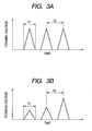
- the voltage waveforms in the case of applying the pulses having the peak values of the constant voltage are shown in Fig. 3A.
- Reference marks T1 and T2 denote the pulse width and the pulse intervals of the voltage waveforms, respectively, in Fig. 3A.
- the pulse width T1 is set to be within a range from 1 ⁇ sec to 10 msec, and the pulse interval T2 is set to be in a range from 10 ⁇ sec to 100 msec.
- the peak values (peak voltages at the time of the forming) of the triangular waves are suitably selected.
- Reference marks T1 and T2 denote the pulse width and the pulse interval of the voltage waveforms, respectively, in Fig. 3B.
- the voltage width T1 is set to be in a range from 1 ⁇ sec to 10 msec
- the pulse interval T2 is set to be in a range from 10 ⁇ sec to 100 msec.
- the peak values (peak voltages at the time of the forming) of the triangular waves increases by, for example, about every 0.1 V step.
- the forming processing is ended at the following time point. That is, a voltage having a degree of a magnitude which does not destroy and deform the electroconductive film 4 locally, for example, a pulse voltage of about 0.1 V, is inserted between the pulses for forming to measure a device current. Thereby, a resistance value is obtained, and the forming processing is ended at the time point when the resistance value shows, for example, a value equal to 1000 times or more of the resistance before the forming processing.
- the forming processing is performed for forming the gap 5 described above by applying the triangular wave pulses between the device electrodes 2 and 3
- the waveform of the wave applied to the part between the device electrodes 2 and 3 is not limited to the triangular wave, and a desired waveform such as a rectangular wave can be used.
- the peak values, the pulse widths, the pulse intervals of the waves are not limited to the values described above, and suitable values are selected according to the resistance value of the electron emitting device, and the like in order that the gap 5 may be formed in a good condition.
- Activation processing is performed to the device in which the forming has ended.
- the activation processing is performed by applying a voltage between the device electrodes 2 and 3 in a suitable degree of vacuum in an atmosphere including a carbon compound gas.
- the carbon films 6a and 6b including carbon or a carbon compound from the carbon compound existing in the atmosphere as the principal components of the carbon films 6a and 6b are deposited on the electroconductive thin films 4a and 4b, and the device current If and the emission current Ie come to change remarkably.
- the carbon and/or the carbon compound here mean ones, for example, graphite (including the so-called HOPG, PG and GC.
- HOPG indicates an almost complete crystal structure of graphite
- PG indicates a somewhat disturbed crystal structure having crystal grains each of a degree of 20 nm
- GC indicates a still largely disturbed crystal structure having crystal grains each of a degree of 2 nm
- amorphous carbon indicating the amorphous carbon, and a mixture of the amorphous carbon and the fine crystal of the graphite.
- aliphatic hydrocarbons such as alkane, alkene and alkyne, aromatic hydrocarbons, alcohols, aldehydes, ketones, amines, organic acids such as phenol, carvone and sulfonic acid, and the like.
- saturation hydrocarbons expressed by C n H 2n+2 such as methane, ethane and propane
- unsaturated hydrocarbon expressed by composition formulae such as C n H 2n such as ethylene and propylene, benzene, toluene, methanol, ethanol, formaldehyde, acetaldehyde, acetone, methyl ethyl ketone, methylamine, ethylamine, phenol, benzonitrile, tolunitrile, formic acid, acetic acid, and propionic acid, and mixtures of them.
- the pulse widths of the bipolar voltage pulse applied between the device electrodes 2 and 3 are set in order to be different from each other.
- the forms of the carbon films 6a and 6b are influenced by the voltage waveforms applied to the device, the pressure of the carbon compound to be introduced, the diffusion mobility on the surface of the device, the average residence time on the surface of the device, and the like. Moreover, the easiness of handling such as the easiness of introduction into the vacuum apparatus and the easiness of the exhaustion after the activation is also important.
- the carbon-containing gas is introduced into the vacuum space through a slow leak valve and a partial pressure thereof is somewhat influenced by the shape of the vacuum apparatus and the members used for the vacuum apparatus.
- the partial pressure is suitable within a range about from 1 ⁇ 10 -5 Pa to 1 ⁇ 10 -2 Pa.
- Fig. 4 shows an example of the waveforms of the activation voltage pulses which can be used suitably for the present invention.
- the maximum voltage value to be applied is suitably selected in a range from 10 to 26 V.
- Reference marks T1 and T1' denote positive and negative pulse widths of the voltage waveforms, respectively.
- a reference mark T2 denotes a pulse interval.
- the pulse width T1 is set to be larger than the pulse width T1'.
- the absolute values of the positive and the negative voltage values are set to be equal to one another.
- the activation process is ended at the time point when the emission current Ie has almost reached its saturation.
- the bipolar voltage pulses having the pulse widths T1 and T1' satisfying the relation T1 > T1' as shown in Fig. 4 are applied during the activation process in the state in which the electric potential of the device electrode 3 is positive, the asymmetrical structure in which the height of the carbon film 6b connected to the device electrode 3 electrically from the surface of the substrate is higher than that of the carbon film 6a connected to the device electrode 2 electrically as shown in Figs. 1A and 1B can be made.
- a stabilization process is preferably performed for the electron-emitting device produced as mentioned above.
- the process is a process for exhausting the carbon compounds in the vacuum chamber.
- the partial pressure of the carbon compounds is preferably 1 ⁇ 10 -8 Pa or less.
- the pressure including the other gases is preferably 1 ⁇ 10 -6 Pa or less, and especially the pressure is more preferably 1 ⁇ 10 -7 Pa or less.
- a vacuum exhausting apparatus which does not use oil is used as the vacuum exhausting apparatus for exhausting the vacuum chamber lest the oil produced from the apparatus should influence the characteristic of the device. To put it concretely, the vacuum exhausting apparatus such as a sorption pump and an ion pump can be cited.
- the whole of the vacuum chamber is heated at the time of the exhaustion of the inside of the vacuum chamber to make it easy to exhaust the carbon compound molecules attached to the inner wall of the vacuum chamber and the electron-emitting device. It is to be desired that the heating is performed for a period of time as long as possible under the heating condition within a range from 150 to 350°C, preferably at 200°C or higher. But, the heating condition is not limited to that condition.
- the heating is performed under a condition suitably selected according to the conditions of the size and the shape of the vacuum chamber, the arrangement of the electron-emitting device, and the like.
- the atmosphere is not limited to that. As long as the carbon compounds are sufficiently removed, the atmosphere can keep a sufficiently stable characteristic even if the pressure itself somewhat rises.
- a metal or a metal compound is deposited on the carbon films 6a and 6b by the oblique evaporation after the stabilization process, and thereby the electron scattering surface forming films 7a and 7b are formed (Fig. 2E).
- the angle of the oblique evaporation is preferably an angle ⁇ 1 within a range from 10° to 90° from the normal vector of the substrate 1 toward the side of the positive electrode (device electrode 3) at the time of the application of the voltages.
- the electron scattering surface forming film 7b completely covers the carbon film 6b on the side of the high potential by the oblique evaporation, the elastic scattering efficiency of electrons on the device electrode 3 on the side of high potential increases, and electron scattering is more effectively produced by an electron scattering body. As a result, the emission current If increases. Moreover, since an electron scattering surface forming film is not formed in the gap 8 owing to the influence of the carbon film 6b on the side of the high potential, the device current If does not change, but only the emission current Ie increases.
- the atomic structure factor, to electron beams, of the metal or the metal compound used at the present process is larger than that of carbon.
- the atomic structure factor E( ⁇ ) e 2 Z/2mv 2 sin 2 ⁇ . Consequently, the atomic structure factor E is in proportion to the atomic number Z, and heavy elements strongly scatter electrons. Therefore, since the atomic structure factor of a larger atomic number to an electron beam is roughly larger, the atomic number of the metal or the metal compound which is evaporated obliquely is preferably larger than that of carbon. Consequently, for example, Pb, Au, Pt, W, Ta, Ba, Hf, and the like are suitable as stable and heavy elements.
- oxides such as PbO and BaO, borides such as HfB 2 and ZrB 2 , carbides such as HfC, ZrC, TaC and WC, and nitrides such as HfN, ZrN and TiN are preferably used.
- the electron scattering surface forming film 7b is formed on the carbon film 6b on the side of the high potential, and further on the high potential side electroconductive thin film 4b and the high potential side device electrode 3, which are on the extension of the carbon film 6b, as the need arises.
- the electron scattering surface forming film 7a may be formed on the low potential side, no electron scattering surface forming film is formed in the gap 5.
- the feature of the electron-emitting device according to the present invention is that the height of the high potential side carbon film 6b is formed to be higher than that of the low potential side carbon film 6a in the direction perpendicular to the surface of the substrate 1.
- the electron-emitting device includes the electron scattering surface forming film 7b having the high efficiency of performing the elastic scattering of the electrons entering the carbon film 6b.
- the basic characteristic of the electron-emitting device according to the present invention is evaluated by a measurement evaluation apparatus shown in Fig. 5. In the following, the measurement evaluation apparatus is described.
- a power supply 51 and an ammeter 50 are connected to the device electrodes 2 and 3, and the anode electrode 54, to which a power supply 53 and an ammeter 52 are connected, is disposed above the electron-emitting device.
- each member of the electron-emitting device is denoted by the same mark as that shown in Figs. 1A and 1B.
- the electron scattering surface forming films 7a and 7b of the electron-emitting device are omitted for convenience.
- the reference numeral 51 denotes the power supply for applying a device voltage Vf to the device
- the reference numeral 50 denotes the ammeter for measuring the device current If flowing the electroconductive thin films 4a and 4b including the electron-emitting region 8 between the device electrodes 2 and 3.
- the reference numeral 54 denotes the anode electrode for catching the emission current Ie emitted from the electron-emitting region 8
- the reference numeral 53 denotes the high-voltage power supply for applying a voltage to the anode electrode 54
- the reference numeral 52 denotes the ammeter for measuring the emission current Ie emitted from the electron-emitting region 8 of the device.
- the present electron-emitting device and the anode electrode 54 are set in a vacuum apparatus 55, and the vacuum apparatus 55 is provided with equipment necessary for the vacuum apparatus 55 such as an exhaust pump 56 and a vacuum gauge (not shown) to make it possible to perform the measurement evaluation of the present device in a desired vacuum.
- the voltage of the anode electrode 54 is measured within a range from 1 kV to 10 kV, and the distance H between the anode electrode 54 and the electron-emitting device is measured within a range from 2 mm to 8 mm.
- An electron source can be configured by arranging a plurality of electron-emitting devices according to the present invention on a substrate, and an image displaying apparatus can be configured by combining the electron source and a phosphor member which emits light by the electrons emitted from the electron-emitting devices.
- an image displaying apparatus can be configured by combining the electron source and a phosphor member which emits light by the electrons emitted from the electron-emitting devices.
- the arrangement of the electron-emitting devices is not especially limited, but the so-called passive matrix arrangement is preferably applied.
- the passive matrix arrangement is an arrangement form in which n Y-direction wires are installed on m X-direction wires with an interlayer insulation layer put between the wires and the X-direction wires and the Y-direction wires are connected to a pair of device electrodes of each of the electron-emitting devices, respectively.
- the passive matrix arrangement is described in detail.
- a reference numeral 71 denotes an electron source base
- a reference numeral 72 denotes the X-direction wires
- a reference numeral 73 denotes the Y-direction wires
- a reference numeral 74 denotes electron-emitting devices.
- the m X-direction wires 72 are composed of wires Dx1, Dx2, ..., Dxm, and consist of an electroconductive metal or the like formed on the base 71 consists of an insulating substrate by the vacuum evaporation method, the printing method, the sputtering method or the like to be a desired pattern.
- the material, the film thicknesses and wiring widths of the X-direction wires 72 are set in order to supply almost equal voltages to many electron-emitting devices.
- the Y-direction wires 73 are composed of n wires Dy1, Dy2, ..., Dyn, and like the X-direction wires 72, the Y-direction wires 73 consist of an electroconductive metal in a desired pattern which is formed by the vacuum evaporation method, the printing method, the sputtering method or the like.
- the material, the film thicknesses and the wiring widths of the Y-direction wires 73 are set in order to supply almost equal voltages to many electron-emitting devices.
- An interlayer insulation layer (not shown) is installed between the m X-direction wires 72 and the n Y-direction wires 73, and thereby the m X-direction wires 72 and the n Y-direction wires 73 are electrically separated.
- matrix wiring is configured (wherein both of m and n indicate positive integers).
- the interlayer insulation layer (not shown) consists of SiO 2 or the like which is formed by the vacuum evaporation method, the printing method, the sputtering method or the like.
- the interlayer insulation layer is formed over the whole of or a part of the surface of the insulating substrate 7, on which the X-direction wires 72 are formed.
- the film thickness, the material and the manufacturing method of the interlayer insulation layer are suitably set in order that the interlayer insulation layer can resist the potential difference at the intersection parts of the X-direction wires 72 and the Y-direction wires 73.
- the X-direction wires 72 and the Y-direction wires 73 are pulled out as external terminals severally.
- opposing device electrodes (not shown) of the electron-emitting devices 74 are electrically connected to the m X-direction wires 72 (Dx1, Dx2, ..., Dxm) and the n Y-direction wires 73 (Dy1, Dy 2 ..., Dyn) through wire connections consist of an electroconductive metal or the like formed by the vacuum evaporation method, the printing method, the sputtering method or the like.
- scanning signal applying means for applying scanning signals for scanning the rows of the electron-emitting devices 74 arranged in the X directions according to an input signal is electrically connected.
- modulating signal generating means for applying modulating signals for modulating each of the columns of the electron-emitting devices 74 arranged in the Y directions according to the input signal is electrically connected.
- the drive voltage applied to each of the electron-emitting devices 74 is supplied as a difference voltage of a scanning signal and a modulating signal applied to the device.
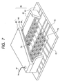
- Fig. 7 is a perspective view schematically showing the basic configuration of a partially broken display panel of an image displaying apparatus.
- Figs. 8A and 8B are plan views of an configuration example of a fluorescent film used for the display panel.
- a reference numeral 81 denotes a rear plate to which the electron source base 71 is fixed
- a reference numeral 86 denotes a face plate composed of a glass substrate 83 on the inner surface of which a fluorescent film 84, a metal-back 85 and the like are formed.
- a reference numeral 82 denotes a supporting frame.
- An envelope 88 is configured by coating frit glass on the rear plate 81, the supporting frame 82 and the face plate 86, and by baking the coated rear plate 81, the supporting frame 82 and the face plate 86 at a temperature within a range from 400 to 500°C for ten minutes or more in the air or in the atmosphere of nitrogen, to perform the seal bonding of them.
- the same members as those shown in Fig. 6 are denoted by the same marks as those in Fig 6.
- the envelope 88 is composed of the face plate 86, the supporting frame 82 and the rear plate 81 as described above, the rear plate 81 is provided chiefly with the aim of reinforcing the strength of the electron source base 71. Consequently, in the case where the base 71 itself has a sufficient strength, the rear plate provided separately is not necessary. Then, the supporting frame 82 may be directly seal-bonded to the base 81, and the envelope 88 may be configured by the face plate 86, the supporting frame 82 and the base 71.
- an envelope 88 having a sufficient strength to the atmospheric pressure also can be configured.
- a reference numeral 91 denotes a black electroconductive material
- a reference numeral 92 denotes a phosphor.
- the fluorescent film 84 consists of only the phosphor 92 in case of monochrome. But, in the case of the fluorescent film of color, the fluorescence film 84 consists of the black electroconductive material 91 and the phosphors 92, which are called as a black stripe (Fig. 8A) or a black matrix (Fig. 8B) according to the arrangement of the phosphors 92.
- the purpose of providing the black stripe or the black matrix is to make the color mixing or the like inconspicuous by blackening the toned portions among the respective phosphors 92 of the three primary color phosphors, which become necessary at the time of color display, and to suppress the lowering of the contrast owing to the reflection of external light on the fluorescent film 84.
- the material of the black electroconductive material 91 there is a material including graphite as the principal component, which is usually used frequently, but the material is not limited to that material. As long as a material having electrical conductivity and the properties of little light transmission and light reflection, the material can be used as the black electroconductive material 91.
- the precipitation method, the printing method and the like are used independent of the monochrome display or the color display.
- the metal-back 85 is usually formed on the inner surface side of the fluorescent film 84.
- the purposes of the provision of the metal-back 85 are raising luminance by performing the mirror reflection of the light toward the inner surface side in the light emitted by the phosphor to the side of the face plate 86, making the metal-back 85 act as an electrode for applying an electron beam accelerating voltage, protecting the phosphor from being damaged by the collision of the negative ions generated in the envelope 88, and the like.
- the metal-back 85 can be produced by performing smoothing processing (usually called as filming) of the surface on the inner surface side of the fluorescent film 84 after the production of the fluorescent film 84, and by depositing aluminum in vacuum evaporation or the like after that.
- a transparent electrode (not shown) may be further provided to the face plate 86 on the outer surface side of the fluorescent film 84.
- each color phosphor should be made to correspond with an electron-emitting device in case of a color display. Accordingly, it is necessary to perform sufficient alignment.
- the sealing of the envelope 88 is performed after making the inside of the envelope 88 be at the degree of vacuum of about 1.3 ⁇ 10 -5 Pa through an exhaust pipe (not shown). Moreover, getter processing is sometimes performed in order to maintain the degree of vacuum after the sealing of the envelope 88.
- the getter processing is the processing of heating a getter (not shown) disposed at a predetermined position in the envelope 88 by a heating method such as the resistance heating or the high frequency heating immediately before of after the sealing of the envelope 88 for forming an evaporated film. Ba or the like is usually the principal component of the getter, and the degree of vacuum within a range, for example, from 1.3 ⁇ 10 -3 Pa to 1.3 ⁇ 10 -5 Pa is kept by the absorption operation of the evaporated film.
- an image is displayed by making each electron-emitting device 74 emit electrons by applying voltages to the X-direction wires 72 and the Y-direction wires 73 through the external terminals of the container, and by accelerating electron beams to collide with the fluorescent film 84 by applying a high voltage equal to several kV or more to the metal-back 85 or the transparent electrode (not shown) through a high-voltage terminal 87, and thereby by performing excitation and light-emission.
- An electron-emitting device having the configuration shown in Figs. 1A and 1B was produced in accordance with the processes shown in Figs. 2A to 2E.
- a pattern to be the device electrodes 2 and 3 and a desired gap L between the device electrodes 2 and 3 was formed on a cleaned quartz substrate 1 with photoresist (RD-2000N-41 made by Hitachi Chemical Co., Ltd.), and Ti and Pt were deposited to be the thicknesses of 5 nm and 30 nm, respectively, in order by the electron beam evaporation method.
- the photoresist pattern was dissolved by an organic solvent, and the lift off of the Pt/Ti deposition films were carried out.
- the device electrode interval L was set to 3 ⁇ m, and the device electrodes 2 and 3 having the width W of 500 ⁇ m of the device electrodes were formed (Fig. 2A).
- a Cr film having a film thickness of 100 nm was deposited by the vacuum evaporation, and the patterning was performed to have an opening corresponding to the form of an electroconductive thin film, which will be described later.
- An organic palladium compound solution (ccp4230 made by Okuno Chemical Industries Co., Ltd.) was coated on the Cr film while being rotated by a spinner, and the heat baking processing at 300°C for 12 minutes was performed.
- the film thickness of the electroconductive thin film 4 which consists of Pd as the principal element formed in the way mentioned above was 10 nm, and the sheet resistance Rs thereof was 2 ⁇ 10 4 ⁇ / ⁇ .
- the Cr film and the electroconductive thin film 4 after baking were etched by an acid etchant, and the electroconductive thin film 4 of a desired pattern with the width W' of the electroconductive thin film 4 being 300 ⁇ m was formed (Fig. 2B).
- the device electrodes 2 and 3 and the electroconductive thin film 4 were formed on the substrate 1.
- devices of comparative examples 1 and 2 were produced by the quite same processes.
- the above-mentioned device was set in the measurement evaluation apparatus of Fig. 5.
- a voltage was applied between the device electrodes 2 and 3 from the power supply 51 for applying the device voltage Vf to the device, and the forming processing was performed.
- the gap 5 was formed in the electroconductive thin film 4, and the electroconductive thin film 4 was separated into the electroconductive thin films 4a and 4b (Fig. 2C).
- the voltage waveforms of the forming processing were ones shown in Fig. 3B.
- the pulse width T1 was set to be 1 msec
- the pulse interval T2 was set to be 16.7 msec.
- the peak values of the triangular waves were raised by a step of 0.1 V to perform the forming processing. Moreover, during the forming processing, a resistance measurement pulse having a voltage of 0.1 V was simultaneously inserted between the pulses for forming to measure the resistance. Incidentally, the end of the forming processing was set at the time when the measured value by the resistance measurement pulse became 1 M ⁇ or more, and the application of the voltages to the device was ended simultaneously.
- tolunitrile was introduced in the vacuum apparatus 1 through the slow leak valve, and the pressure of 1.0 ⁇ 10 -4 Pa was maintained.
- the activation processing of the device which had processed by the forming processing was performed using the waveform shown in Fig. 4 through the device electrodes 2 and 3, in which waveform the pulse width T1 was set to 1 msec, the pulse width T1' was set to 0.1 msec, the pulse interval T2 was set to 10 msec, and the maximum voltage values were set to be ⁇ 22 V.
- the voltages given to the device electrode 3 were made to be positive, and the direction of the device current If flowing from the device electrode 3 to the device electrode 2 was set to be positive.
- current conduction was stopped, and the slow leak valve was closed to end the activation processing.
- the device of the comparative example 1 was produced according to the completely same process.
- the activation processing similar to that of the device of the present example except for the setting of the pulse width T1 being 1 msec, the pulse width T1' being 1 msec, and the pulse interval T2 being 10 msec in the waveform shown in Fig. 4 was performed to the device of the comparative example 2 which had received the same forming process as that of the device of the present example.
- a stabilization process was performed.
- the exhausting of the inside of the vacuum apparatus was continued while keeping the vacuum apparatus and the electron-emitting device at about 250°C by heating them with a heater.
- the heating with the heater was stopped after 20 hours, and the temperature of the inside of the vacuum apparatus was returned to the room temperature. Then, the pressure in the inside of the vacuum apparatus reached about 1 ⁇ 10 -8 Pa.
- the distance H between the anode electrode 54 and the electron-emitting device was set to 4 mm, and the electric potential of 1 kV was given to the anode electrode 54 with the high voltage power supply 53.
- rectangular pulse voltages having the peak values of 15 V were applied between the device electrodes 2 and 3 with the power supply 51, and the device currents If and the emission currents Ie of the device of the example and the devices of the comparative examples were measured with the ammeter 50 and the ammeter 52, respectively.
- no stable emission currents Ie could be measured because large leakage currents flowed.
- the device of the present example had a large emission current Ie and a superior electron emission efficiency ⁇ in comparison with the devices of the comparative examples.
- the observations of the forms of the planes including the electron-emitting regions 8 of the devices were performed using the atomic force microscope.
- the form of the device of the present example was the same as the plane form shown in Figs. 1A and 1B. That is, the carbon films 6a and 6b and the electron scattering surface forming films 7a and 7b were observed on both the sides of the gap 5 formed in the electroconductive thin film 41.
- the height of the highest portion of the electron scattering surface forming film is at a position higher by about 80 nm from the surfaces of the electroconductive thin films 4a and 4b, and the electron scattering surface forming film 7b at the height had the belt-like form having an width of about 50 nm.
- the observation of the electron scattering surface forming film was similarly performed to the device of the comparative example 2.
- the height of the electron scattering surface forming film was almost uniform, and no belt-like forms like the device of the present example were observed.
- Example 1 The processes of the Example 1 were performed until the Process d except that a substrate of soda lime glass with SiO 2 coated thereon was used as the substrate 1.
- tolunitrile was introduced in the vacuum apparatus through the slow leak valve, and the pressure of 1.0 ⁇ 10 4 Pa was maintained.
- the activation processing of the device which had received the forming processing was performed with the waveform shown in Fig. 4, in which the pulse width T1 was set to 1 msec, the pulse width T1' was set to 0.1 msec, the pulse interval T2 was set to 10 msec, and the maximum voltage values were set to ⁇ 22 V, through the device electrodes 2 and 3 of the device.
- the voltage given to the device electrode 3 was made to be positive, and the direction of the device current If flowing from the device electrode 3 to the device electrode 2 was positive.
- current conduction was stopped, and the slow leakage valve was closed, and then the activation processing was ended.
- the activation process was performed to the device of a comparative example 3, which had received the same forming process as that of the device of the present example, under the conditions described above.
- the stabilization process was performed.
- the exhaustion of the inside of the vacuum apparatus was continued while the vacuum apparatus and the electron-emitting device were heated by a heater to be kept at about 250°C.
- the heating with the heater was stopped after 20 hours, and the temperatures of the vacuum apparatus and the electron-emitting device were returned to the room temperature. Then, the pressure in the vacuum apparatus reached about 1 ⁇ 10 -8 Pa.
- Pt atomic number 78
- the oblique evaporation was performed by several atomic layers by inclining the evaporation molecule beam flow coming flying from a heated evaporation source by the angle ⁇ 1 equal to 45° from the normal line of the substrate 1 after the forming processing.
- a part of Pt was also stacked on the substrate 1, the device electrodes 2 and 3, and the thin films 4a and 4b including the electron-emitting region 8, no evils owing to the stacking were produced.
- an electron scattering surface forming film was formed in the device of the comparative example 3 by the same method as that of the device of the present example except for the angle ⁇ 1 of the oblique evaporation was set to -45°.
- the distance H between the anode electrode 54 and the electron-emitting device was set to 4 mm, and the electric potential of 1 kV was given to the anode electrode 54 with the high voltage power supply 53.
- rectangular pulse voltages having peak values of 15 V were applied between the device electrodes 2 and 3 with the power supply 51, and the device currents If and the emission currents Ie of the device of the present example and the device of the comparative example 3 were measured with the ammeters 50 and 52, respectively.
- no stable emission currents Ie could measured because large leakage current flowed.
- the device of the present example had the large emission current Ie and the excellent electron emission efficiency ⁇ in comparison with the device of the comparative example 3.
- the shape of the present example was one including the same carbon films 6a and 6b and the electron scattering surface forming films 7a and 7b as those of the shape shown in Figs. 1A and 1B.
- a plurality of pairs of device electrodes 2 and 3 was formed on the substrate 1 (Fig. 9).
- a film of titanium Ti was formed to be a thickness of 5 nm on the glass substrate 1 and a film of platinum Pt was formed to be a thickness of 40 nm on the Ti film, both formed by the sputtering method as under coating layers.
- photoresist was coated on the Pt film, and the patterning for forming the device electrodes 2 and 3 was performed by the photolithographic method composed of a series of processes of exposure, development and etching to form the device electrodes 2 and 3.
- each of the intervals L of the device electrodes 2 and 3 was 10 ⁇ m, and the corresponding length W was 100 ⁇ m.
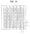
- the Y-direction wires (lower wires) 73 as common wires were formed to be in a line-like pattern in order to contact with the device electrodes 3 in order to connect them each other (Fig. 10).
- As the material of the wires 73 a silver Ag photopaste ink was used, and the photopaste ink was printed on the substrate 1 by the screen printing method. After that, the photopase ink was dried, and was exposed to be a predetermined pattern to be developed. After that, the substrate 1 was baked at a temperature around 480°C, and wirers were formed.
- the thicknesses of the wires were about 10 ⁇ m and each of the line widths was 50 ⁇ m. Incidentally, the ends of the wires were formed to have large line widths in order to use as the electrodes for taking out the wires.
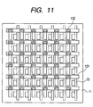
- interlayer insulation layers 131 were arranged (Fig. 11).
- the interlayer insulation layers 131 were formed under the X-direction wires (upper wires) 72, which will be described later, to cover the intersection parts with the Y-direction wires (lower wires) 73, and contact holes 132 were opened at connection parts with the device electrodes 2 for enabling the electrical connection with the device electrodes 2.
- the process of the formation of the insulating layer was as follows. After a photosensitive glass paste including PbO as its principal component was printed by the screen printing method, the glass paste was exposed and developed. The process was repeated four times, and, finally, the glass paste was baked at the temperature around 480°C.
- the thicknesses of the interlayer insulation layers 131 were about 30 ⁇ m in all, and each of the widths of the interlayer insulation layers 131 were 150 ⁇ m.
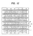
- a Ag paste ink was printed on the interlayer insulation layers 131 formed in the previous process by the screen printing method, and was dried after that. The same process was performed on the printed Ag paste again as two-times coating. After that, the Ag paste was baked at a temperature around 480°C, and the X-direction wires (upper wires) 72 were formed (Fig. 12). The X-direction wires 72 intersected with the Y-direction wires (lower wires) 73 with the insulated layers 131 put between them, and the X-direction wires 72 were also contacted with the device electrodes 2 at the contact hole 132 portions.
- the device electrodes 2 are connected to one another, and the X-direction wires 72 operate as scanning electrodes after being made to be a panel.
- the thicknesses of the X-direction wires 72 are about 15 ⁇ m. Extraction wires to an external drive circuit were also formed by the same method as the one described above.
- extraction terminals to the external drive circuit were also formed by the same method as the one described above.
- An electron source base including the XY matrix wiring was formed in this way.
- the surface thereof was processed with the solution containing a water repellency agent to make the surface thereof have a hydrophobic property.
- the formation of the surface to have the hydrophobic property aims that the aqueous solution for the formation of the electroconductive thin films 4 which are applied after this process is disposed with a suitable spread on the device electrodes.
- the electroconductive thin films 4 were formed by the ink jet coating method between the device electrodes 2 and 3 (Fig. 13).
- a schematic diagram of the process is shown in Figs. 14A and 14B.
- a reference numeral 161 denotes droplet giving means
- a reference numeral 162 denotes a droplet.
- the droplets 162 of the solution were adjusted so that the diameters of dots might be set to 60 ⁇ m, and the droplets 162 were given between the device electrodes 2 and 3.
- the heating baking processing of the substrate 1 was performed at 350°C for 10 minutes, and the droplets 162 were made to palladium oxide (PdO). Films having the diameters of the dots being about 60 ⁇ m and the film thicknesses being 10 nm at the maximum were obtained.
- the films of palladium oxide PdO were formed in the electroconductive thin film portions.
- the resistance values of the electroconductive thin films 4 of the electron source base were within a range from 3500 ⁇ to 4500 ⁇ .
- reference numeral 181 denotes an exhaust pump
- a reference numeral 182 denotes an exhaust valve
- a reference numeral 183 denotes a vacuum chamber
- a reference numeral 184 denotes a vacuum gauge
- a reference numeral 185 denotes an ammeter
- a reference numeral 186 denotes gas bombs
- a reference numeral 187 denotes a wire.
- the electron source base 71 which had not received the forming was put in the vacuum chamber 183, and the pressure in the vacuum chamber 183 was set to 1.3 ⁇ 10 -3 Pa or less.
- a mixed gas of 98% of N 2 and 2% of H 2 was introduced into the vacuum chamber 183, and the pressure therein was set to 5 ⁇ 10 -2 Pa.
- the electron source base 71 was held for 30 minutes in that state, the resistance values of the electroconductive thin films of the electron source were monitored with the ammeter 185. After that, each electron source was reduced, and the resistance values became within a range from 500 ⁇ to 2000 ⁇ . After that, the reducing gas was exhausted, and the electron source base 71 was taken out from the vacuum chamber 183.
- a reference numeral 171 denotes a common electrode
- a reference numeral 172 denotes a pulse generator
- a reference numeral 173 denotes a control switching circuit
- a reference numeral 174 denotes a vacuum apparatus.
- Fig. 15 by connecting the external terminals Dy1 to Dyn of the Y-direction wires 73 to the common electrode 171, the Y-direction wires 73 are commonly connected, and Y-direction wires 73 are connected to the terminal on the side of the ground of the pulse generator 172.
- the control switching circuit 173 connects each terminal to either the pulse generator 172 or the ground, and Fig. 15 shows the function thereof schematically.
- the forming processing was performed by the method of selecting one row of the device rows in the X directions with the switching circuit 173, switching the device row to be selected every application of one pulse, and processing all of the device rows simultaneously.
- the waveforms of the applied pulse voltages are the triangular wave pulses the peak values of which gradually increase as shown in Fig. 3B.
- the pulse width T1 was set to 1 msec, and the pulse interval T2 was set to 10 msec.
- a rectangular wave pulse having peak value of 0.1 V was inserted between the above-mentioned pulses, and the resistance value of the device was measured.
- the activation processing was carried out by repeatedly applying pulse voltages to the device electrodes through the XY direction wiring from the exterior, At this process, tolunitrile was used as carbon or the like, and the tolunitrile was introduced into the vacuum space to maintain the pressure of 1.3 ⁇ 10 -4 Pa.
- the activation processing was performed under the setting of the waveform shown in Fig. 4 in which the pulse width T1 on the positive side was set to 1 msec, the pulse width T1' on the negative side was set to 0.1 msec, the pulse interval T2 was set to 10 msec, and the maximum voltage values were set to ⁇ 22 V. In this case, the electrode 3 sides were made positive. At the time point when the device current If had reached almost saturation after about 60 minutes from the start, current conduction was stopped, and the introduction of the tolunitrile was stopped. Then, the activation processing was ended.
- the electron scattering surface forming film was formed. While the pressure in the vacuum apparatus was kept to 1 ⁇ 10 -8 Pa, the oblique evaporation of Pt (atomic number 78) as a material having a large atomic structure factor to electron beams was carried out from the electrode 3 sides as the electron scattering surface forming films.
- Pt atomic number 78
- the processing was performed to all the electron source devices.
- the faceplate 86 (composed of the glass substrate 83, the fluorescent film 84, which is the image forming member, and the metal-back 85.
- the fluorescent film 84 and the metal-back 85 were formed on the inner surface of the glass substrate 83) was disposed at a position above the substrate 71 by 5 mm with the supporting frame 82 put between the faceplate 86 and the substrate 71.
- frit glass was applied to the joining part of the faceplate 86, the supporting frame 82 and the rear plate 81.
- the seal bonding was performed by baking the panel in the air at 400°C for ten minutes.
- the fixation of the substrate 71 to the rear plate 81 was also performed with the frit glass.
- the phosphor in the stripe form (see Fig. 8A) was used as the fluorescent film 84, which is an image forming member.
- the black stripe which consisted of a black electroconductive material 91 was formed first, and each color phosphor 92 was coated at the gap parts of the black electroconductive material 91 by the slurry method. Thereby, the fluorescent film 84 was produced.
- the black electroconductive material 91 a material including graphite as its principal component, which was usually frequently used, was used.
- the metal-back 85 was formed on the inner side of the fluorescent film 84.
- the metalback 85 was produced by performing smoothing processing (usually called as filming) of the inner side surface of the fluorescent film 84 after the production of the fluorescent film 84, and then by evaporating A1 thereon in the vacuum.
- the inside of the vacuum chamber (envelope 88) formed as mentioned above was exhausted while heating the vacuum chamber.
- the exhaust pipe (not shown) was heated with a gas burner to be welded. Thereby, the vacuum chamber was sealed. Furthermore, getter processing was performed by high frequency heating in order to maintain the pressure in the vacuum chamber to be low.
- a desired electron-emitting device was selected through the X-direction wires and the Y-direction wires.
- a pulse voltage of +20 V was applied on the electrode 3 side and a voltage of 8 kV was applied to the metal back 85 through the high-voltage terminal Hv, a bright good image was able to be formed over a long time.
- An electron-emitting device is equipped with a pair of first electroconductive members arranged on a substrate with an interval between them, wherein the interval becomes narrower at an upper position distant from a surface of the substrate than at a position on the surface, and a peak of one of the pair of the first electroconductive members is higher than a peak of the other of the pair of the first electroconductive members, and further an electron scattering surface forming film including an element having an atomic number larger than those of elements constituting the first electroconductive members as a principal component is provided on a surface of the one of the first electroconductive members.
Landscapes
- Engineering & Computer Science (AREA)
- Manufacturing & Machinery (AREA)
- Cold Cathode And The Manufacture (AREA)
- Cathode-Ray Tubes And Fluorescent Screens For Display (AREA)
Applications Claiming Priority (2)
| Application Number | Priority Date | Filing Date | Title |
|---|---|---|---|
| JP2004125255 | 2004-04-21 | ||
| JP2004125255A JP4366235B2 (ja) | 2004-04-21 | 2004-04-21 | 電子放出素子、電子源及び画像表示装置の製造方法 |
Publications (2)
| Publication Number | Publication Date |
|---|---|
| EP1596408A2 true EP1596408A2 (fr) | 2005-11-16 |
| EP1596408A3 EP1596408A3 (fr) | 2008-05-21 |
Family
ID=34935186
Family Applications (1)
| Application Number | Title | Priority Date | Filing Date |
|---|---|---|---|
| EP05008198A Withdrawn EP1596408A3 (fr) | 2004-04-21 | 2005-04-14 | Dispositif émetteur d'électrons, source d'électrons et procédé de fabrication d'un dispositif d'affichage d'images |
Country Status (4)
| Country | Link |
|---|---|
| US (1) | US7312561B2 (fr) |
| EP (1) | EP1596408A3 (fr) |
| JP (1) | JP4366235B2 (fr) |
| CN (1) | CN100530486C (fr) |
Families Citing this family (17)
| Publication number | Priority date | Publication date | Assignee | Title |
|---|---|---|---|---|
| US7471801B2 (en) * | 2002-05-10 | 2008-12-30 | Osseofon Ab | Device for the generation of or monitoring of vibrations |
| JP3740485B2 (ja) * | 2004-02-24 | 2006-02-01 | キヤノン株式会社 | 電子放出素子、電子源、画像表示装置の製造方法及び駆動方法 |
| JP4366235B2 (ja) * | 2004-04-21 | 2009-11-18 | キヤノン株式会社 | 電子放出素子、電子源及び画像表示装置の製造方法 |
| US7230372B2 (en) * | 2004-04-23 | 2007-06-12 | Canon Kabushiki Kaisha | Electron-emitting device, electron source, image display apparatus, and their manufacturing method |
| JP3907667B2 (ja) * | 2004-05-18 | 2007-04-18 | キヤノン株式会社 | 電子放出素子、電子放出装置およびそれを用いた電子源並びに画像表示装置および情報表示再生装置 |
| JP3935478B2 (ja) * | 2004-06-17 | 2007-06-20 | キヤノン株式会社 | 電子放出素子の製造方法およびそれを用いた電子源並びに画像表示装置の製造方法および該画像表示装置を用いた情報表示再生装置 |
| JP3774723B2 (ja) | 2004-07-01 | 2006-05-17 | キヤノン株式会社 | 電子放出素子の製造方法およびそれを用いた電子源並びに画像表示装置の製造方法、該製造方法によって製造された画像表示装置を用いた情報表示再生装置 |
| JP4594077B2 (ja) * | 2004-12-28 | 2010-12-08 | キヤノン株式会社 | 電子放出素子及びそれを用いた電子源並びに画像表示装置および情報表示再生装置 |
| JP2008027853A (ja) * | 2006-07-25 | 2008-02-07 | Canon Inc | 電子放出素子、電子源および画像表示装置、並びに、それらの製造方法 |
| EP2109132A3 (fr) * | 2008-04-10 | 2010-06-30 | Canon Kabushiki Kaisha | Appareil de faisceau à électrons et appareil d'affichage d'image l'utilisant |
| JP2009277460A (ja) * | 2008-05-14 | 2009-11-26 | Canon Inc | 電子放出素子及び画像表示装置 |
| JP2009277458A (ja) * | 2008-05-14 | 2009-11-26 | Canon Inc | 電子放出素子及び画像表示装置 |
| JP2009277457A (ja) * | 2008-05-14 | 2009-11-26 | Canon Inc | 電子放出素子及び画像表示装置 |
| JP2010092843A (ja) * | 2008-09-09 | 2010-04-22 | Canon Inc | 電子線装置およびそれを用いた画像表示装置 |
| JP4637233B2 (ja) * | 2008-12-19 | 2011-02-23 | キヤノン株式会社 | 電子放出素子の製造方法及びこれを用いた画像表示装置の製造方法 |
| JP2010146914A (ja) * | 2008-12-19 | 2010-07-01 | Canon Inc | 電子放出素子の製造方法および画像表示装置の製造方法 |
| JP2010182585A (ja) * | 2009-02-06 | 2010-08-19 | Canon Inc | 電子放出素子及びこれを用いた画像表示装置 |
Citations (3)
| Publication number | Priority date | Publication date | Assignee | Title |
|---|---|---|---|---|
| EP0725413A1 (fr) | 1995-01-31 | 1996-08-07 | Canon Kabushiki Kaisha | Dispositif émetteur d'électrons ainsi qu'une source d'électrons et appareil de formation d'images utilisant de tels dispositifs |
| EP0899766A2 (fr) | 1995-01-31 | 1999-03-03 | Canon Kabushiki Kaisha | Procédé de formations d'images avec un dispositif d'émission d'électrons |
| EP1009009A2 (fr) | 1998-12-08 | 2000-06-14 | Canon Kabushiki Kaisha | Dispositif émetteur d'électrons, source d'électrons utilisant ces dispositifs émetteurs d'électrons, et dispositif de formation d'images utilisant cette source d'électrons |
Family Cites Families (29)
| Publication number | Priority date | Publication date | Assignee | Title |
|---|---|---|---|---|
| US4904895A (en) | 1987-05-06 | 1990-02-27 | Canon Kabushiki Kaisha | Electron emission device |
| US5066883A (en) | 1987-07-15 | 1991-11-19 | Canon Kabushiki Kaisha | Electron-emitting device with electron-emitting region insulated from electrodes |
| US5749763A (en) | 1987-07-15 | 1998-05-12 | Canon Kabushiki Kaisha | Display device with electron-emitting device with electron-emitting region insulted from electrodes |
| US5412285A (en) * | 1990-12-06 | 1995-05-02 | Seiko Epson Corporation | Linear amplifier incorporating a field emission device having specific gap distances between gate and cathode |
| US6313815B1 (en) | 1991-06-06 | 2001-11-06 | Canon Kabushiki Kaisha | Electron source and production thereof and image-forming apparatus and production thereof |
| CA2137721C (fr) | 1993-12-14 | 2000-10-17 | Hidetoshi Suzuki | Source d'electrons et sa methode de fabrication et appareil d'imagerie et sa methode de fabrication |
| CA2126535C (fr) | 1993-12-28 | 2000-12-19 | Ichiro Nomura | Appareil a faisceau electronique et appareil d'imagerie |
| JP3332676B2 (ja) * | 1994-08-02 | 2002-10-07 | キヤノン株式会社 | 電子放出素子、電子源及び画像形成装置と、それらの製造方法 |
| US6246168B1 (en) * | 1994-08-29 | 2001-06-12 | Canon Kabushiki Kaisha | Electron-emitting device, electron source and image-forming apparatus as well as method of manufacturing the same |
| US6473063B1 (en) | 1995-05-30 | 2002-10-29 | Canon Kabushiki Kaisha | Electron source, image-forming apparatus comprising the same and method of driving such an image-forming apparatus |
| JP3174999B2 (ja) * | 1995-08-03 | 2001-06-11 | キヤノン株式会社 | 電子放出素子、電子源、それを用いた画像形成装置、及びそれらの製造方法 |
| EP0936651B1 (fr) | 1998-02-12 | 2004-08-11 | Canon Kabushiki Kaisha | Procédé de fabrication d'un élément émetteur d'électrons. source d'électrons, et dispositif de formation d'images |
| JP3320387B2 (ja) | 1998-09-07 | 2002-09-03 | キヤノン株式会社 | 電子源の製造装置及び製造方法 |
| JP2000155555A (ja) | 1998-09-16 | 2000-06-06 | Canon Inc | 電子放出素子の駆動方法及び、該電子放出素子を用いた電子源の駆動方法、並びに該電子源を用いた画像形成装置の駆動方法 |
| JP3135118B2 (ja) | 1998-11-18 | 2001-02-13 | キヤノン株式会社 | 電子源形成用基板、電子源及び画像形成装置並びにそれらの製造方法 |
| JP3530823B2 (ja) | 1999-01-19 | 2004-05-24 | キヤノン株式会社 | 画像形成装置の製造方法 |
| JP3323848B2 (ja) | 1999-02-26 | 2002-09-09 | キヤノン株式会社 | 電子放出素子およびこれを用いた電子源およびこれを用いた画像形成装置 |
| JP3323851B2 (ja) | 1999-02-26 | 2002-09-09 | キヤノン株式会社 | 電子放出素子およびこれを用いた電子源およびこれを用いた画像形成装置 |
| JP3323852B2 (ja) | 1999-02-26 | 2002-09-09 | キヤノン株式会社 | 電子放出素子およびこれを用いた電子源およびこれを用いた画像形成装置 |
| JP3634757B2 (ja) | 2001-02-02 | 2005-03-30 | 株式会社三井ハイテック | リードフレーム |
| JP3634852B2 (ja) | 2002-02-28 | 2005-03-30 | キヤノン株式会社 | 電子放出素子、電子源及び画像表示装置の製造方法 |
| JP3740485B2 (ja) | 2004-02-24 | 2006-02-01 | キヤノン株式会社 | 電子放出素子、電子源、画像表示装置の製造方法及び駆動方法 |
| KR20050096541A (ko) * | 2004-03-31 | 2005-10-06 | 삼성에스디아이 주식회사 | 돌출부를 갖는 네거티브 홀 구조, 그것의 형성 방법 및그것을 포함하는 fed 캐소드 부 |
| US7271529B2 (en) | 2004-04-13 | 2007-09-18 | Canon Kabushiki Kaisha | Electron emitting devices having metal-based film formed over an electro-conductive film element |
| JP4366235B2 (ja) * | 2004-04-21 | 2009-11-18 | キヤノン株式会社 | 電子放出素子、電子源及び画像表示装置の製造方法 |
| US7230372B2 (en) | 2004-04-23 | 2007-06-12 | Canon Kabushiki Kaisha | Electron-emitting device, electron source, image display apparatus, and their manufacturing method |
| JP3907667B2 (ja) | 2004-05-18 | 2007-04-18 | キヤノン株式会社 | 電子放出素子、電子放出装置およびそれを用いた電子源並びに画像表示装置および情報表示再生装置 |
| JP3935478B2 (ja) | 2004-06-17 | 2007-06-20 | キヤノン株式会社 | 電子放出素子の製造方法およびそれを用いた電子源並びに画像表示装置の製造方法および該画像表示装置を用いた情報表示再生装置 |
| JP3774723B2 (ja) | 2004-07-01 | 2006-05-17 | キヤノン株式会社 | 電子放出素子の製造方法およびそれを用いた電子源並びに画像表示装置の製造方法、該製造方法によって製造された画像表示装置を用いた情報表示再生装置 |
-
2004
- 2004-04-21 JP JP2004125255A patent/JP4366235B2/ja not_active Expired - Fee Related
-
2005
- 2005-04-14 EP EP05008198A patent/EP1596408A3/fr not_active Withdrawn
- 2005-04-15 US US11/106,584 patent/US7312561B2/en not_active Expired - Fee Related
- 2005-04-20 CN CNB2005100673568A patent/CN100530486C/zh not_active Expired - Fee Related
Patent Citations (3)
| Publication number | Priority date | Publication date | Assignee | Title |
|---|---|---|---|---|
| EP0725413A1 (fr) | 1995-01-31 | 1996-08-07 | Canon Kabushiki Kaisha | Dispositif émetteur d'électrons ainsi qu'une source d'électrons et appareil de formation d'images utilisant de tels dispositifs |
| EP0899766A2 (fr) | 1995-01-31 | 1999-03-03 | Canon Kabushiki Kaisha | Procédé de formations d'images avec un dispositif d'émission d'électrons |
| EP1009009A2 (fr) | 1998-12-08 | 2000-06-14 | Canon Kabushiki Kaisha | Dispositif émetteur d'électrons, source d'électrons utilisant ces dispositifs émetteurs d'électrons, et dispositif de formation d'images utilisant cette source d'électrons |
Also Published As
| Publication number | Publication date |
|---|---|
| JP2005310524A (ja) | 2005-11-04 |
| CN1691242A (zh) | 2005-11-02 |
| US7312561B2 (en) | 2007-12-25 |
| EP1596408A3 (fr) | 2008-05-21 |
| JP4366235B2 (ja) | 2009-11-18 |
| US20050236952A1 (en) | 2005-10-27 |
| CN100530486C (zh) | 2009-08-19 |
Similar Documents
| Publication | Publication Date | Title |
|---|---|---|
| US7312561B2 (en) | Electron-emitting device, electron source, and method for manufacturing image displaying apparatus | |
| US7582002B2 (en) | Manufacturing method of electron emitting device, electron source and image display apparatus | |
| US20090244398A1 (en) | Electron-emitting device, electron-emitting apparatus, electron source, image display device and information display/reproduction apparatus | |
| JP2000285801A (ja) | 電子放出素子の製造方法、該電子放出素子を用いた電子源および画像形成装置 | |
| US6582268B1 (en) | Electron-emitting device, electron source and manufacture method for image-forming apparatus | |
| EP2120246A2 (fr) | Dispositif d'émission d'électrons et appareil d'affichage d'images | |
| US7442406B2 (en) | Electron-emitting device, electron source substrate, electron beam apparatus, display apparatus, and manufacturing method thereof | |
| US6586872B2 (en) | Electron emission source, method and image-forming apparatus, with enhanced output and durability | |
| EP2120247B1 (fr) | Dispositif émetteur d'électrons et appareil d'affichage d'images | |
| US7755267B2 (en) | Electron emitting device having electroconductive thin film and high resistivity sheet | |
| JP2009277457A (ja) | 電子放出素子及び画像表示装置 | |
| JP3397569B2 (ja) | 表面伝導型電子放出素子およびその製造方法、ならびに同電子放出素子を備えた電子源、画像形成装置 | |
| US6755709B2 (en) | Method of fabricating electron-emitting device, electron source and image-forming apparatus using the electron source | |
| JP2000195415A (ja) | 電子放出素子、電子源、画像形成装置及びそれらの製造方法 | |
| JP3200270B2 (ja) | 表面伝導型電子放出素子、電子源、及び、画像形成装置の製造方法 | |
| EP1032012B1 (fr) | Dispositif émetteur d'électrons,source d'électrons et procédé de fabrication d'un appareil de formation d'images | |
| JP2001351548A (ja) | 平板型画像形成装置及びその製造方法 | |
| JP2000243236A (ja) | 電子放出素子、電子源基板及び画像形成装置 | |
| JP2006019248A (ja) | 電子放出素子、電子源、画像表示装置、及び電子放出素子の製造方法 | |
| JP2000164117A (ja) | 電子放出素子、電子源、画像形成装置及びそれらの製造方法 | |
| JP2000251627A (ja) | 電子源基板及びそれを用いた画像形成装置 | |
| JP2003086083A (ja) | 電子放出素子、電子源基板、画像形成装置、及びそれらの製造方法 | |
| JP2006134592A (ja) | 電子放出素子、電子源、及び、画像形成装置の製造方法 | |
| JP2000243231A (ja) | 電子源基板およびそれを用いた画像形成装置 | |
| JP2000251632A (ja) | 電子源基板及びそれを用いた画像形成装置 |
Legal Events
| Date | Code | Title | Description |
|---|---|---|---|
| PUAI | Public reference made under article 153(3) epc to a published international application that has entered the european phase |
Free format text: ORIGINAL CODE: 0009012 |
|
| AK | Designated contracting states |
Kind code of ref document: A2 Designated state(s): AT BE BG CH CY CZ DE DK EE ES FI FR GB GR HU IE IS IT LI LT LU MC NL PL PT RO SE SI SK TR |
|
| AX | Request for extension of the european patent |
Extension state: AL BA HR LV MK YU |
|
| PUAL | Search report despatched |
Free format text: ORIGINAL CODE: 0009013 |
|
| AK | Designated contracting states |
Kind code of ref document: A3 Designated state(s): AT BE BG CH CY CZ DE DK EE ES FI FR GB GR HU IE IS IT LI LT LU MC NL PL PT RO SE SI SK TR |
|
| AX | Request for extension of the european patent |
Extension state: AL BA HR LV MK YU |
|
| RIC1 | Information provided on ipc code assigned before grant |
Ipc: H01J 31/12 20060101ALI20080417BHEP Ipc: H01J 9/02 20060101ALI20080417BHEP Ipc: H01J 1/316 20060101AFI20080417BHEP |
|
| 17P | Request for examination filed |
Effective date: 20081121 |
|
| AKX | Designation fees paid |
Designated state(s): DE FR GB IT NL |
|
| 17Q | First examination report despatched |
Effective date: 20090717 |
|
| GRAP | Despatch of communication of intention to grant a patent |
Free format text: ORIGINAL CODE: EPIDOSNIGR1 |
|
| RIN1 | Information on inventor provided before grant (corrected) |
Inventor name: KOBAYASHI, TAMAKI, Inventor name: YAMAMOTO, KEISUKE, Inventor name: TAKEDA, TOSHIHIKO, Inventor name: MORIGUCHI, TAKUTO, |
|
| STAA | Information on the status of an ep patent application or granted ep patent |
Free format text: STATUS: THE APPLICATION HAS BEEN WITHDRAWN |
|
| 18W | Application withdrawn |
Effective date: 20120725 |