EP1579574B1 - Ac powered logic circuitry - Google Patents
Ac powered logic circuitry Download PDFInfo
- Publication number
- EP1579574B1 EP1579574B1 EP03814771A EP03814771A EP1579574B1 EP 1579574 B1 EP1579574 B1 EP 1579574B1 EP 03814771 A EP03814771 A EP 03814771A EP 03814771 A EP03814771 A EP 03814771A EP 1579574 B1 EP1579574 B1 EP 1579574B1
- Authority
- EP
- European Patent Office
- Prior art keywords
- circuit
- logic gate
- gate
- power
- logic
- Prior art date
- Legal status (The legal status is an assumption and is not a legal conclusion. Google has not performed a legal analysis and makes no representation as to the accuracy of the status listed.)
- Expired - Lifetime
Links
Images


Classifications
-
- H—ELECTRICITY
- H03—ELECTRONIC CIRCUITRY
- H03K—PULSE TECHNIQUE
- H03K19/00—Logic circuits, i.e. having at least two inputs acting on one output; Inverting circuits
-
- G—PHYSICS
- G06—COMPUTING OR CALCULATING; COUNTING
- G06K—GRAPHICAL DATA READING; PRESENTATION OF DATA; RECORD CARRIERS; HANDLING RECORD CARRIERS
- G06K19/00—Record carriers for use with machines and with at least a part designed to carry digital markings
- G06K19/06—Record carriers for use with machines and with at least a part designed to carry digital markings characterised by the kind of the digital marking, e.g. shape, nature, code
- G06K19/067—Record carriers with conductive marks, printed circuits or semiconductor circuit elements, e.g. credit or identity cards also with resonating or responding marks without active components
- G06K19/07—Record carriers with conductive marks, printed circuits or semiconductor circuit elements, e.g. credit or identity cards also with resonating or responding marks without active components with integrated circuit chips
- G06K19/0701—Record carriers with conductive marks, printed circuits or semiconductor circuit elements, e.g. credit or identity cards also with resonating or responding marks without active components with integrated circuit chips at least one of the integrated circuit chips comprising an arrangement for power management
-
- G—PHYSICS
- G06—COMPUTING OR CALCULATING; COUNTING
- G06K—GRAPHICAL DATA READING; PRESENTATION OF DATA; RECORD CARRIERS; HANDLING RECORD CARRIERS
- G06K19/00—Record carriers for use with machines and with at least a part designed to carry digital markings
- G06K19/06—Record carriers for use with machines and with at least a part designed to carry digital markings characterised by the kind of the digital marking, e.g. shape, nature, code
- G06K19/067—Record carriers with conductive marks, printed circuits or semiconductor circuit elements, e.g. credit or identity cards also with resonating or responding marks without active components
- G06K19/07—Record carriers with conductive marks, printed circuits or semiconductor circuit elements, e.g. credit or identity cards also with resonating or responding marks without active components with integrated circuit chips
- G06K19/0723—Record carriers with conductive marks, printed circuits or semiconductor circuit elements, e.g. credit or identity cards also with resonating or responding marks without active components with integrated circuit chips the record carrier comprising an arrangement for non-contact communication, e.g. wireless communication circuits on transponder cards, non-contact smart cards or RFIDs
-
- G—PHYSICS
- G06—COMPUTING OR CALCULATING; COUNTING
- G06K—GRAPHICAL DATA READING; PRESENTATION OF DATA; RECORD CARRIERS; HANDLING RECORD CARRIERS
- G06K19/00—Record carriers for use with machines and with at least a part designed to carry digital markings
- G06K19/06—Record carriers for use with machines and with at least a part designed to carry digital markings characterised by the kind of the digital marking, e.g. shape, nature, code
- G06K19/067—Record carriers with conductive marks, printed circuits or semiconductor circuit elements, e.g. credit or identity cards also with resonating or responding marks without active components
- G06K19/07—Record carriers with conductive marks, printed circuits or semiconductor circuit elements, e.g. credit or identity cards also with resonating or responding marks without active components with integrated circuit chips
- G06K19/077—Constructional details, e.g. mounting of circuits in the carrier
-
- H—ELECTRICITY
- H03—ELECTRONIC CIRCUITRY
- H03K—PULSE TECHNIQUE
- H03K19/00—Logic circuits, i.e. having at least two inputs acting on one output; Inverting circuits
- H03K19/02—Logic circuits, i.e. having at least two inputs acting on one output; Inverting circuits using specified components
- H03K19/08—Logic circuits, i.e. having at least two inputs acting on one output; Inverting circuits using specified components using semiconductor devices
- H03K19/094—Logic circuits, i.e. having at least two inputs acting on one output; Inverting circuits using specified components using semiconductor devices using field-effect transistors
-
- H—ELECTRICITY
- H03—ELECTRONIC CIRCUITRY
- H03K—PULSE TECHNIQUE
- H03K3/00—Circuits for generating electric pulses; Monostable, bistable or multistable circuits
- H03K3/02—Generators characterised by the type of circuit or by the means used for producing pulses
- H03K3/027—Generators characterised by the type of circuit or by the means used for producing pulses by the use of logic circuits, with internal or external positive feedback
- H03K3/03—Astable circuits
- H03K3/0315—Ring oscillators
Definitions
- the invention relates to logic circuitry.
- Thin film circuit devices including transistors, diodes, and the like, are widely used in a variety of modem electronic devices, including integrated circuits, printed circuit boards, flat panel displays, smart cards, cell phones, and radio frequency identification (RFID) tags.
- Thin film circuit devices are typically formed by depositing, masking and etching a variety of conducting, semiconducting and insulating layers to form a thin film stack.
- thin film transistors are based on inorganic semiconductor materials such as amorphous silicon or cadmium selenide. More recently, significant research and development efforts have been directed to the use of organic semiconductor materials to form thin film transistor circuitry.
- Organic semiconductor materials offer a number of manufacturing advantages for transistor fabrication.
- organic semiconductor materials permit the fabrication of organic thin film transistors (OTFTs) on flexible substrates such as thin glass, polymeric or paper-based substrates.
- organic semiconductor materials can be formed using low-cost fabrication techniques such as printing, embossing or shadow masking.
- OTFTs organic thin film transistors
- US 570 1093 discloses transistors being gate-source coupled FETs functioning as diodeses so that an intermediate rectifier circuitry is provided, generating a dc voltage to power the logic circuitry.
- the invention is directed to logic circuitry powered by alternating current (ac) power sources.
- the invention may be applied to logic circuitry incorporating thin film transistors based on amorphous or polycrystalline organic semiconductors, inorganic semiconductors or combinations of both.
- an ac power source to power thin film transistor-based logic circuitry can support satisfactory device performance for a variety of applications, while enhancing long-term stability of the circuitry.
- the OTFT circuitry may exhibit stable performance characteristics over an extended period of operation.
- Enhanced stability may permit the use of OTFT circuitry to form a variety of thin film transistor-based logic circuit devices, including inverters, oscillators, logic gates, registers and the like.
- logic circuit devices may find utility in a variety of applications, including integrated circuits, printed circuit boards, flat panel displays, smart cards, cell phones, and RFID tags.
- ac-powered thin film transistor circuitry may eliminate the need for an ac to dc rectification block, thereby reducing the manufacturing time, expense, cost, complexity, and size of the component carrying the thin film transistor circuitry.
- the ac power source directly powers the logic gate circuitry.
- the ac power source applies an ac power waveform to one or more individual logic gates, instead of applying dc power to the logic gates via an ac-dc rectification block.
- the invention provides an electronic circuit comprising a first transistor and a second transistor arranged to form a logic gate, and an alternating current (ac) source to directly power the logic gate with an ac power waveform.
- the invention provides a method comprising directly powering a logic gate formed by at least a first transistor and a second transistor with an alternating current (ac) power waveform produced by an alternating current (ac) power source.
- the invention provides a radio frequency identification (RFID) tag comprising a logic gate formed by at least a first transistor and a second transistor, and a radio frequency converter that converts RF energy to alternating current (ac) power, and directly powers the logic gate with the ac power.
- RFID radio frequency identification
- the invention provides a radio frequency identification (RFID) system comprising an RFID tag including first and second transistors arranged to form a logic gate, a radio frequency (RF) converter that converts RF energy to alternating current (ac) power and directly powers the logic gate with the ac power, and a modulator that conveys information, and an RFID reader that transmits the RF energy to the RFID tag for conversion by the RF converter, and reads the information conveyed by the modulator.
- RFID radio frequency identification
- the invention provides a ring oscillator circuit comprising a plurality of transistors arranged to form a series of inverter stages, the inverter stages being coupled to form a ring oscillator, and an alternating current (ac) source to directly power the inverter stages in the ring oscillator with an ac power waveform.
- ac alternating current
- ac-powered logic circuitry and particularly OTFT-based logic circuitry, may exhibit increased stability over an extended period of time, relative to dc-powered thin film transistor circuitry.
- ac-powered thin film transistor circuitry may maintain oscillation amplitudes over a longer period of time relative to dc-powered thin film transistor circuitry.
- OTFT circuitry may promote wider use of OTFT circuitry in a variety of applications, with more reliable performance, durability and longevity. Consequently, various applications for OTFT circuitry may benefit from manufacturing advantages associated with OTFT circuitry, such as the ability to form circuitry on flexible substrates, such as thin glass, polymeric or paper-based substrates, and use lower-cost manufacturing techniques.
- the use of ac power for the thin film transistor circuitry may eliminate the need for the ac-dc rectifier component otherwise required in some applications for delivery of dc power to the circuitry. Accordingly, by eliminating the need for a rectifier component, the use of ac power may reduce the manufacturing time, expense, cost, complexity, and size of components carrying thin film transistor circuitry.
- ac-powered thin film circuitry may substantially reduce the cost and size of the tag by eliminating the ac-dc rectifier component.
- ac-powered thin film logic circuitry can result in substantial cost and size savings in the design and manufacture of the RFID tag.
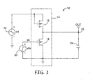
- FIG. 1 is a circuit diagram illustrating an ac-powered inverter circuit.
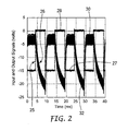
- FIG. 2 is a graph illustrating simulated performance of the inverter circuit of FIG. 1 .
- FIG. 3 is a circuit diagram illustrating an ac-powered inverter circuit based on complementary metal oxide semiconductor (CMOS) transistors.
- CMOS complementary metal oxide semiconductor
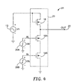
- FIG. 4 is a circuit diagram illustrating an ac-powered NAND gate circuit.
- FIG. 5 is a circuit diagram illustrating an ac-powered thin film transistor-based NOR gate circuit.
- FIG. 6 is a circuit diagram illustrating an ac-powered thin film transistor-based ring oscillator circuit with load capacitors.
- FIG. 7 is a graph illustrating simulated performance of the ring oscillator circuit of FIG. 6 .
- FIG. 8 is a circuit diagram illustrating an ac-powered thin film transistor -based ring oscillator circuit without load capacitors.
- FIG. 9 is a graph illustrating simulated performance of the ring oscillator circuit of FIG. 8 .
- FIG. 10 is a block diagram illustrating application of ac-powered thin film transistor circuitry in an RFID tag/reader system.
- FIG. 11 is a circuit diagram further illustrating the RFID tag/reader system of FIG. 10 .
- FIG. 12 is a circuit diagram further illustrating a reader associated with the RFID tag/reader system of FIG. 10 .
- FIG. 13 is a graph illustrating simulated output of an RFID tag constructed using ac-powered thin film transistor circuitry.
- FIG. 14 is a circuit diagram illustrating an ac-powered inverter circuit that drives a liquid crystal display element.
- FIG. 15 is a circuit diagram illustrating an ac-powered inverter circuit that drives a light emitting diode (LED).
- LED light emitting diode
- FIG. 1 is a circuit diagram illustrating an ac-powered inverter circuit 10.
- Inverter circuit 10 may include an ac power source 12 that supplies ac power to a logic gate in the form of an inverter 14 having a load transistor 16 and a drive transistor 18.
- Each transistor 16, 18 may be a thin film field effect transistor, and may be based on an amorphous or polycrystalline inorganic or organic semiconducting material.
- organic semiconducting materials such as pentacene may be used to form OTFTs.
- circuit 10 may be formed by a combination of organic and inorganic semiconducting material, e.g., to form a complementary metal oxide semiconductor (CMOS) inverter circuit.
- CMOS complementary metal oxide semiconductor
- inverter circuit 10 may be formed by an NMOS inorganic field effect transistor and a PMOS organic field effect transistor.
- transistors 16, 18 may be especially adaptable to fabrication using low cost fabrication techniques, and may be formed on flexible substrates for some applications.
- the ac power source 12 directly powers inverter 14 with an ac power waveform.
- the ac power is applied directly to inverter 14 in the sense that the inverter receives an ac power waveform instead of dc power produced by an ac-dc rectification component.
- inverter 14 operates in response to an ac power waveform.
- intervening circuitry may exist between ac power source 12 and inverter 14 provided that the inverter still receives an ac power waveform as operating power, rather than a dc power signal.
- the ac power waveform is applied directly across the common gate and drain connection of load transistor 16 and the ground connection coupled to the source of drive transistor 18.
- ac power source 12 to power thin film transistor-based logic circuitry, such as inverter 14 in FIG. 1 , can support satisfactory device performance for a variety of applications, while enhancing long-term stability of the circuitry.
- the inverter when inverter 14 is powered by ac power source 12, the inverter may exhibit stable performance characteristics over an extended period of operation relative to dc-powered inverters, especially for organic semiconducting materials.
- ac operation of inverter 14 will eliminate the need for an ac-dc rectifier component to power the inverter.
- the ac power waveform supplied to inverter circuit 10 may have a variety of regular shapes, e.g., sinusoidal, square, or sawtooth-shaped.
- the ac power waveform may have irregular shapes. Accordingly, the ac power waveform exhibits an alternating current flow but is not limited to any particular shape. Nevertheless, in many applications, the ac power waveform may be a sinusoidal waveform.
- the gate and drain of load transistor 16 are coupled to ac power supply 12.
- the drain of drive transistor 18 is coupled to the source of load transistor 16, and the source of the drive transistor is coupled to ground.
- a signal source 20 drives the gate of drive transistor 18, e.g., with a logic signal.
- inverter 14 produces an inverted output 22, which may be output across a load capacitor 24.
- Load capacitor 24 serves to filter out some of the ac voltage present at the output and provides for a cleaner output signal. The amount of filtering depends on the capacitance of load capacitor 24 and the frequency of the ac power.
- Load capacitor 24 may be formed by an input capacitance produced by gate/source overlap within a logic gate coupled to output 22 in the event inverter circuit 10 is coupled to drive one or more additional logic gates.
- the gate/source overlap may be controlled during manufacture of a drive transistor 18 in a subsequent logic gate to produce a desired level of capacitance in load capacitor 24.
- load capacitor 24 may be formed independently, particularly if output 22 does not drive another logic gate.
- load transistor 16 may have a gate width to gate length ratio that is greater than or equal to a gate width to gate length ratio of the drive transistor 18. In this case, direct current (dc) powering of the circuit would result in inferior operation of the logic gate, for NMOS or PMOS designs, because of the reduced gain. NMOS or PMOS ring oscillators based on this design, for example, would not operate if powered by direct current.
- An added benefit of having the gate width to gate length ratio of load transistor 16 greater or equal to the drive transistor 18 gate width to gate length ratio is that the total circuit area can be reduced.
- FIG. 2 is a graph illustrating simulated performance of the inverter circuit 10 of FIG. 1 .
- the graph illustrates signal voltage transitions over a period of time.
- transistors 16, 18 are modeled as PMOS organic field effect transistors.
- trace 25 is the input signal waveform applied to the gate of drive transistor 18 by signal source 20.
- Trace 26 is the output signal waveform produced by inverter 14 at output 22.
- the input signal waveform transitions between a logic '0' state 28 and a logic '1' state 27.
- inverter 14 produces an inverted output in response to the input signal waveform, i.e., a logic '1' state 32 and a logic '0' state 30, as shown in FIG. 2 .
- Inverter 14 exhibits a propagation delay that is inversely related to the ac voltage applied to load transistor 16 and the mobility of the semiconductor material forming the inverter, and proportional to the parasitic capacitance within transistors 16, 18 and any external capacitance that may be independently added to inverter circuit 10.
- the ac power source 12 may have a frequency characterized by a period that is less than the propagation delay time of inverter 14.
- ac power source 12 produces a sinusoidal waveform having a frequency of 125 kHz and a peak-to-peak amplitude of 80 volts.
- signal source 20 produces a square wave input signal waveform between approximately 0 and - 15 volts, at approximately 100 Hz.
- Inverter 14 turns “on” in response to the ac power supply waveform applied by ac power source 12, and serves to invert the input signal waveform applied by signal source 20.
- the output 22 of inverter 14 may be applied to additional logic circuitry.
- a plurality of inverters 14 may be combined to form a variety of logic components, such as oscillators, logic gates, registers and the like.
- inverter circuit 10 is depicted in FIG. 1 for use as a logic gate, the inverter circuit may be used as an analog amplifier in some cases.
- inverter circuit 10 can be used to drive a variety of loads, including display elements such as liquid crystal display (LCD) elements, or light emitting diodes (LEDs), including organic light emitting diodes (OLEDs).
- display elements such as liquid crystal display (LCD) elements, or light emitting diodes (LEDs), including organic light emitting diodes (OLEDs).
- LEDs light emitting diodes
- OLEDs organic light emitting diodes
- FIG. 3 is a circuit diagram illustrating an ac-powered thin film transistor-based inverter circuit 14' incorporating CMOS-based circuitry.
- the source of p-channel transistor 16 is coupled to ac power supply 12.
- An n-channel transistor 19 has a drain coupled to the drain of transistor 16.
- the gates of transistors 16, 19 are coupled together and driven by a signal source 20.
- Signal source 20 drives the gates of transistors 16, 19, e.g., with a logic signal.
- the source of transistor 19 is coupled to ground.
- the source of transistor 16 and the drain of transistor 19 are coupled together to form the output 22 of inverter circuit 14'.
- inverter 14' produces an inverted output 22.
- a load capacitor may be coupled between output 22 and ground.
- the load capacitor may be formed by the input capacitance of a subsequent logic gate coupled to the output of inverter circuit 14'.
- a load capacitor may be formed independently to provide the desired load capacitance for output 22.
- FIG. 4 is a circuit diagram illustrating an ac-powered thin film transistor-based NAND gate circuit 21.
- the gate and drain of load transistor 16 are coupled to ac power supply 12.
- the drain of first drive transistor 18A is coupled to the source of load transistor 16.
- the drain of second drive transistor 18B is coupled to the source of first drive transistor 18A.
- the source of second drive transistor 18B is coupled to ground.
- First and second signal sources 20A, 20B drive the gates of drive transistors 18A, 18B, respectively.
- NAND gate 23 produces a logical NAND output 22.
- Transistors 16, 18A, 18B form a NAND gate.
- NAND circuit 21 is operative in response to the ac power supply signal delivered directly to the NAND circuit by ac power supply 12.
- a load capacitor may be coupled across output 22.
- the load capacitor may be formed independently or realized by the input capacitance of a logic gate driven by output 22 of NAND circuit 21.
- FIG. 5 is a circuit diagram illustrating an ac-powered thin film transistor-based NOR gate circuit 25.
- FIG. 5 represents another example of a thin film transistor-based logic circuit that operates with an ac power supply, in accordance with the invention.
- the gate and drain of load transistor 16 are coupled to ac power supply 12.
- Transistors 16, 29A, 29B form a NOR gate 27.
- the drains of first and second drive transistors 29A, 29B are coupled to the source of load transistor 16, and to output 22.
- the sources of first and second drive transistors 29A, 29B are coupled to ground.
- First and second signal sources 31A, 31B drive the gates of drive transistors 29A, 29B, respectively.
- NOR gate 27 produces a logical NOR output 22.
- NOR circuit 25 is operative in response to the ac power supply signal delivered by ac power supply 12.
- a load capacitor may be coupled across logical NOR output 22.
- the load capacitor may be formed independently or realized by the input capacitance of a logic gate driven by output 22 of NOR circuit 25.
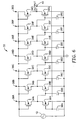
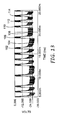
- FIG. 6 is a circuit diagram illustrating an ac-powered thin film transistor-based ring oscillator circuit 33.
- Ring oscillator circuit 33 is an example of another circuit that can be implemented using ac-powered logic gates, e.g., including inverter stages based on OTFTs. As shown in FIG. 6 , ring oscillator circuit 33 includes an odd number of inverter stages arranged in series. In the example of FIG. 6 , ring oscillator circuit 33 includes seven inverter stages 36A-36G having, respectively, load transistors 34A-34G and drive transistors 35A-35G, respectively. Each transistor 34, 35 in ring oscillator circuit 33 is an ac-powered thin film field effect transistor. For example, ac power source 12 delivers ac power to the gates and drains of load transistors 34. The source electrodes of drive transistors 35 are coupled to ground.
- each inverter stage 36 has an output coupled across a respective load capacitor 38A-38G.
- the output of inverter stage 36A is coupled across load capacitor 38B
- the output of inverter stage 36G is coupled across load capacitor 38A.
- Each capacitor 38 may be formed by the input capacitance produced by gate/source overlap within a drive transistor 35 of a subsequent inverter stage 36 that is driven by the output of a respective inverter stage.
- the output 40 of final inverter stage 36G is coupled to the gate of drive transistor 35A in first inverter stage 36A to provide feedback.
- ring oscillator circuit 33 provides a clock signal.
- the output of each inverter stage 36 in ring oscillator circuit 33 can be tapped to provide a clock signal with a desired phase.
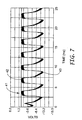
- FIG. 7 is a graph illustrating simulated performance of the ring oscillator circuit 33 of FIG. 6 .
- ring oscillator 33 produces, as output 41, an oscillating output waveform 41 characterized by high peaks 42 and low peaks 43.
- ac power source 12 produces a sinusoidal waveform having a frequency of 125 kHz and a peak-to-peak amplitude of 40 volts.
- Oscillating output waveform 41 in FIG. 7 exhibits a frequency of approximately 300 Hz.
- the output waveform produced by a ring oscillator circuit will have a frequency that is dependent on the number of inverter stages 36 and the propagation delays produced by the individual inverter stages. The propagation delay is inversely related to the ac power supply voltage applied to ring oscillator circuit 33 and the mobility of the semiconducting material, and proportional to any applicable parasitic or external capacitance present in inverter stages 36.
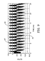
- FIG. 8 is a circuit diagram illustrating an ac-powered thin film transistor-based ring oscillator circuit 33' without capacitors 38.
- FIG. 9 is a graph illustrating simulated performance of the ring oscillator circuit 33' of FIG. 8 .
- Ring oscillator circuit 33' of FIG. 8 conforms substantially to ring oscillator circuit 33 of FIG. 6 , but does not include capacitors 38 at the outputs of respective inverter stages 36. In the absence of capacitors 38, the oscillating output waveform 41', in FIG. 9 including peaks 44 and 46, reveals more of the 125 KHz ac power supply waveform.
- ring oscillator circuit 33 Operation of thin film transistor circuitry, such as ring oscillator circuit 33, also is possible with higher ac power supply frequencies.
- Functioning ring oscillator circuits that conform substantially to circuit 33 have been observed to operate, for example, with ac power supply frequencies on the order of 6 MHz. With increased semiconductor mobility, it may be reasonable to expect use of ring oscillator circuits as described herein with ac power supply frequencies of greater than 10 MHz.
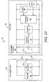
- FIG. 10 is a block diagram illustrating application of ac-powered thin film transistor-based circuitry in an RFID tag/reader system 55.
- ac-powered thin film transistor-based circuitry may be particularly desirable in an RFID tag for a number of reasons, as will be described.
- system 55 may include a reader unit 56 and an RFID tag 58.
- Reader unit 56 may include a radio frequency (RF) source 62 and a reader 64.
- RF source 62 transmits RF energy to RFID tag 58 to provide a source of power.
- RFID tag 58 need not carry an independent power supply, such as a battery. Instead, RFID tag 58 is powered across a wireless air interface between reader unit 56 and the RFID tag.
- reader unit 56 includes an inductor 59 that serves, in effect, as an antenna to transmit and receive RF energy.
- RFID tag 58 may include an ac power source 66.
- ac power source 66 may serve to convert RF energy transmitted by reader unit 56 into ac power for delivery to thin film transistor circuitry carried by RFID tag 58.
- RFID tag 58 may receive the RF energy from reader unit 56 via an inductor 67 that serves as a receiver.
- a capacitor 77 also may be provided in parallel with inductor 67.
- RFID tag 58 further includes a clock circuit 68, data circuit 70, control logic circuit 72, output buffer circuit 74 and modulation inverter 76, one or more of which may be formed by an arrangement of thin film transistor circuitry.
- Clock 68 drives control logic circuit 72 to output data from data circuit 70, which may comprise a plurality of data lines carrying an identification code.
- Output buffer circuit 74 buffers the output from control logic circuit 72.
- Modulation inverter 76 modulates the buffered output for interpretation by reader unit 56 via inductor 67.
- modulation inverter 76 conveys the information by modulating the signal applied across inductor 67.
- FIG. 11 is a circuit diagram further illustrating the RFID tag/reader system 55 of FIG. 10 .
- RF source 62 may include an ac generator 71 that transmits an ac output signal via inductor 59.
- ac generator 71 may take the form of a sinusoidal current source with an output of approximately 0 to 5 amps at a frequency of approximately 125 kHz.
- Inductors 59 and 67 form a transformer for electromagnetic coupling of RF energy between RF source and RFID tag 58. Resistor 73 is selected to limit current.
- the output of ac power source 66 is a sinusoidal waveform with a frequency of approximately 125 kHz. This waveform is then applied to clock circuit 68, control logic 72, data lines 70 and output buffer 74 as represented in FIG. 11 by the terminals AC POWER and COMMON.
- FIG. 11 depicts an RFID tag 58 that carries an n-bit identification code.
- RFID tag 58 carries a 7-bit identification code specified by data lines 70.
- RFID tag 58 may carry a much larger identification code, e.g., 31-bit, 63-bit or 127-bit codes.
- selected data lines 70 may carry information used for start bit identification, data stream synchronization and error checking.
- clock circuit 68 is a ring oscillator formed by a series of seven inverter stages arranged in a feedback loop.
- the ring oscillator of FIG. 11 may be similar to ring oscillator 33 or 33' of FIGS. 6 and 8 .
- the outputs of two successive inverters are applied to a respective NOR gate provided in control logic 72.
- seven NOR gates are used to generate a sequence of seven pulses within each clock cycle produced by the ring oscillator.
- Switches shown in series with data lines 70 are connected to respective NOR gate outputs at one end. If a switch is closed, the respective data line couples the NOR gate output to ground If the switch is open, the NOR gate output is coupled as one of the inputs to a 7-input OR gate within control logic 72.
- the switches for second and fourth data lines are closed.
- data lines 70 store the 7-bit identification code "1010111.”
- the switches can be made, for example, from metal lines that extend from the NOR gate outputs to ground.
- the electrical connections to ground can be intentionally broken or connected during manufacturing to produce, in effect, an open switch, and thereby encode a unique identification code into data lines 70 of RFID tag 58.
- the electrical connections may be broken by a variety of manufacturing techniques such as, for example, laser etching, mechanical scribing, electrical fusing, or shadow masking.
- the output of the 7-input OR gate in control logic 72 is applied to a cascade of buffer amplifiers in output buffer 74 to help match the output impedance of the logic circuitry to the input impedance of the modulation inverter 76.
- the output of the buffer amplifiers in output buffer 74 is applied to the input of the modulation inverter 76.
- the signal TAG OUTPUT is applied to the gate of the drive transistor associated with modulation inverter 76.
- Modulation inverter 76 then modulates the Q of the tank formed by inductor 67 and capacitor 77 to provide amplitude modulation of the carrier signal.
- the received buffer output is conveyed to reader unit 56 so that the identification code can be read by reader 64.
- reader 64 processes the signal received at L_tap via inductor 59.
- FIG. 12 is a circuit diagram further illustrating reader 64 associated with the RFID tag/reader system 55 of FIG. 10 .
- Reader 64 receives, via L_tap, a signal containing the carrier signal, e.g., at 125kHz, modulated by the TAG OUPUT signal, which may be on the order of 1kHz, depending on the frequency of clock circuit 68.
- a low junction capacitance signal diode 78 is used to demodulate the signal.
- a low pass filter section 80 removes the carrier frequency, and may include inductor 84, capacitor 86, resistor 88, inductor 90, capacitor 92 and resistor 94.
- An amplifier stage 82 includes an amplifier 98 in a non-inverting configuration, with resistor 96 and feedback resistor 100 coupled to the inverting input.
- FIG. 13 is a graph illustrating simulated output of an RFID tag constructed using ac-powered thin film transistor circuitry as shown in FIGS. 10-12 .
- FIG. 13 shows the transition of the signal TAG OUTPUT generated from output buffer 74.
- the circuitry is operative to produce a train of pulses in sequence with the clock circuit 68.
- FIG. 13 shows a transition between bit 0 (102), bit 1 (104), bit 2 (106), bit 3 (108), bit 4 (110), bit 5 (112) and bit 6 (114) of the identification code specified by data lines 70.
- the 7-bit code transitions from high to low in a pattern corresponding to the code 1010111. Accordingly, such a pattern can be readily resolved by reader 64 to determine the identification code carried by RFID tag 58.
- FIG. 14 is a circuit diagram illustrating an ac-powered thin film transistor-based inverter circuit 116 that drives a liquid crystal display element 118.
- inverter circuit 116 conforms substantially to inverter circuit 10 of FIG. 1 .
- the output of inverter 14 drives a liquid crystal display element 118.
- one electrode of liquid crystal display element 118 is coupled to the source of load transistor 16 and the drain of drive transistor 18.
- the other electrode of liquid crystal display element 118 is coupled to ground.
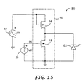
- FIG. 15 is a circuit diagram illustrating an ac-powered thin film transistor-based inverter circuit 120 that drives a light emitting diode (LED) 122.
- Inverter circuit 120 conforms substantially to inverter circuit 10 of FIG. 1 , but drives an LED 122.
- the cathode of LED 122 is coupled to the source of load transistor 16 and the drain of drive transistor 18, and the anode of the LED is coupled to ground.
- ac-powered logic circuitry and particularly OTFT-based logic circuitry, may exhibit stable performance over a longer period of time, relative to dc-powered thin film circuitry.
- dc-powered OTFT logic circuitry appears to undergo substantial changes in threshold voltage over time, the overall performance of ac-powered OTFT logic circuitry does not seem to change as quickly. Instead, ac-powered OTFT circuitry seems to be more stable over an extended period of time.
- ac-powered OTFT circuitry appears to maintain oscillation amplitudes over a much longer period of time relative to dc-powered OTFT circuitry.
- the oscillation amplitude can exhibit a rather rapid decrease.
- the rapid decrease does not occur.
- consistent oscillation amplitude has been observed for an ac-powered OTFT-based ring oscillator running continuously for over sixty hours, in contrast to a dc-powered OTFT-based ring oscillator which exhibited performance changes in less than ten minutes.
- OTFT circuitry may promote wider use of OTFT circuitry in a variety of applications, with more reliable performance, durability and longevity. Consequently, various applications for ac-powered OTFT circuitry, including those described herein, may benefit from manufacturing advantages associated with OTFT circuitry, such as the ability to form circuitry on flexible substrates and use lower-cost manufacturing techniques.
- the use of ac power for the thin film circuitry may eliminate the need for the ac-dc rectifier circuitry otherwise required in some applications for delivery of dc power to the circuitry. Accordingly, by eliminating the need for rectifier circuitry, the use of ac power may reduce the manufacturing time, expense, cost, complexity, and size of components carrying thin film circuitry.
- the use of ac-powered thin film circuitry may substantially reduce the cost and size of the circuit by eliminating the ac-dc rectifier circuitry.
- the RFID tag may benefit from performance and reliability advantages associated with ac-powered OTFT circuitry, possibly creating new opportunities for application of RFID technology.
- the increased reliability of ac-powered OTFTs may permit applications in which the RFID tag, in whatever form, is in more continuous or even persistent operation in conjunction with a reader unit.
- Thin film transistors useful in forming ac-powered logic circuitry may take a variety of forms and may be manufactured using various manufacturing processes.
- the thin film transistors may include organic semiconducting material, inorganic semiconducting material, or a combination of both.
- organic and inorganic semiconducting materials can be used to form CMOS thin film transistor circuitry.
- Thin film transistors useful in forming ac-powered logic circuitry as described herein may include, without limitation, thin film transistors manufactured according to the techniques described in U.S. Patent No. 6,433,359 ; U.S. patent application serial no. 10/012,654, filed November 2, 2001 ; U.S. patent application serial no.
Landscapes
- Engineering & Computer Science (AREA)
- Computer Hardware Design (AREA)
- Physics & Mathematics (AREA)
- Microelectronics & Electronic Packaging (AREA)
- Theoretical Computer Science (AREA)
- General Physics & Mathematics (AREA)
- Computing Systems (AREA)
- Mathematical Physics (AREA)
- General Engineering & Computer Science (AREA)
- Power Engineering (AREA)
- Computer Networks & Wireless Communication (AREA)
- Thin Film Transistor (AREA)
- Logic Circuits (AREA)
- Electronic Switches (AREA)
- Electrophonic Musical Instruments (AREA)
- Ignition Installations For Internal Combustion Engines (AREA)
Applications Claiming Priority (3)
| Application Number | Priority Date | Filing Date | Title |
|---|---|---|---|
| US328461 | 1989-03-24 | ||
| US10/328,461 US7088145B2 (en) | 2002-12-23 | 2002-12-23 | AC powered logic circuitry |
| PCT/US2003/039746 WO2004062106A1 (en) | 2002-12-23 | 2003-12-15 | Ac powered logic circuitry |
Publications (2)
| Publication Number | Publication Date |
|---|---|
| EP1579574A1 EP1579574A1 (en) | 2005-09-28 |
| EP1579574B1 true EP1579574B1 (en) | 2011-07-13 |
Family
ID=32594478
Family Applications (1)
| Application Number | Title | Priority Date | Filing Date |
|---|---|---|---|
| EP03814771A Expired - Lifetime EP1579574B1 (en) | 2002-12-23 | 2003-12-15 | Ac powered logic circuitry |
Country Status (8)
| Country | Link |
|---|---|
| US (2) | US7088145B2 (enExample) |
| EP (1) | EP1579574B1 (enExample) |
| JP (1) | JP4550590B2 (enExample) |
| KR (1) | KR20050088209A (enExample) |
| CN (2) | CN102289705A (enExample) |
| AT (1) | ATE516627T1 (enExample) |
| AU (1) | AU2003297054A1 (enExample) |
| WO (1) | WO2004062106A1 (enExample) |
Families Citing this family (34)
| Publication number | Priority date | Publication date | Assignee | Title |
|---|---|---|---|---|
| US7973313B2 (en) | 2003-02-24 | 2011-07-05 | Semiconductor Energy Laboratory Co., Ltd. | Thin film integrated circuit device, IC label, container comprising the thin film integrated circuit, manufacturing method of the thin film integrated circuit device, manufacturing method of the container, and management method of product having the container |
| DE10329655A1 (de) * | 2003-07-01 | 2005-02-03 | Infineon Technologies Ag | Elektronisches Bauelement |
| US7124942B2 (en) * | 2003-12-05 | 2006-10-24 | Hid Corporation | Low voltage signal stripping circuit for an RFID reader |
| US7768405B2 (en) * | 2003-12-12 | 2010-08-03 | Semiconductor Energy Laboratory Co., Ltd | Semiconductor device and manufacturing method thereof |
| KR101207442B1 (ko) | 2003-12-15 | 2012-12-03 | 가부시키가이샤 한도오따이 에네루기 켄큐쇼 | 박막 집적회로장치의 제조방법, 비접촉형 박막 집적회로장치 및 그 제조 방법, 비접촉형 박막 집적회로 장치를 가지는 아이디 태그 및 동전 |
| US7078937B2 (en) * | 2003-12-17 | 2006-07-18 | 3M Innovative Properties Company | Logic circuitry powered by partially rectified ac waveform |
| KR101161361B1 (ko) * | 2004-03-26 | 2012-06-29 | 가부시키가이샤 한도오따이 에네루기 켄큐쇼 | 반도체장치 |
| DE102005009820A1 (de) * | 2005-03-01 | 2006-09-07 | Polyic Gmbh & Co. Kg | Elektronikbaugruppe mit organischen Logik-Schaltelementen |
| DE102005009819A1 (de) * | 2005-03-01 | 2006-09-07 | Polyic Gmbh & Co. Kg | Elektronikbaugruppe |
| DE102005017655B4 (de) * | 2005-04-15 | 2008-12-11 | Polyic Gmbh & Co. Kg | Mehrschichtiger Verbundkörper mit elektronischer Funktion |
| DE102005031448A1 (de) | 2005-07-04 | 2007-01-11 | Polyic Gmbh & Co. Kg | Aktivierbare optische Schicht |
| DE102005035590A1 (de) * | 2005-07-29 | 2007-02-01 | Polyic Gmbh & Co. Kg | Elektronisches Bauelement |
| DE102005035589A1 (de) | 2005-07-29 | 2007-02-01 | Polyic Gmbh & Co. Kg | Verfahren zur Herstellung eines elektronischen Bauelements |
| DE102005042166A1 (de) * | 2005-09-06 | 2007-03-15 | Polyic Gmbh & Co.Kg | Organisches Bauelement und ein solches umfassende elektrische Schaltung |
| DE102005044306A1 (de) * | 2005-09-16 | 2007-03-22 | Polyic Gmbh & Co. Kg | Elektronische Schaltung und Verfahren zur Herstellung einer solchen |
| US7550998B2 (en) * | 2005-10-26 | 2009-06-23 | Motorola, Inc. | Inverter circuit having a feedback switch and methods corresponding thereto |
| JP2007122981A (ja) * | 2005-10-26 | 2007-05-17 | Matsushita Electric Works Ltd | 点灯装置及び照明装置 |
| US20070215709A1 (en) * | 2006-03-15 | 2007-09-20 | 3M Innovative Properties Company | Rfid sensor |
| KR101478810B1 (ko) * | 2006-07-28 | 2015-01-02 | 가부시키가이샤 한도오따이 에네루기 켄큐쇼 | 축전 장치 |
| US8232621B2 (en) * | 2006-07-28 | 2012-07-31 | Semiconductor Energy Laboratory Co., Ltd. | Semiconductor device |
| KR100790761B1 (ko) * | 2006-09-29 | 2008-01-03 | 한국전자통신연구원 | 인버터 |
| KR100816498B1 (ko) * | 2006-12-07 | 2008-03-24 | 한국전자통신연구원 | 표면 처리된 층을 포함하는 유기 인버터 및 그 제조 방법 |
| CN101212865B (zh) * | 2006-12-29 | 2011-01-19 | 财团法人工业技术研究院 | 以有机晶体管为基础的印刷电路单元 |
| US7982492B2 (en) * | 2009-06-13 | 2011-07-19 | Triune Systems, Lp | Adaptive termination |
| JP5185357B2 (ja) * | 2009-12-17 | 2013-04-17 | 株式会社半導体エネルギー研究所 | 半導体装置 |
| TWI418072B (zh) * | 2010-05-28 | 2013-12-01 | Nat Univ Tsing Hua | 以紙做為基板並以蠶絲做為介電材料之有機薄膜電晶體及其製作方法 |
| CN102270743A (zh) * | 2010-06-04 | 2011-12-07 | 国立清华大学 | 使用纸基板及蚕丝介电层的有机薄膜晶体管及其制作方法 |
| US8362813B2 (en) | 2011-03-24 | 2013-01-29 | Pericom Semiconductor Corp. | Re-driver with pre-emphasis injected through a transformer and tuned by an L-C tank |
| US9077245B2 (en) * | 2011-09-16 | 2015-07-07 | North Carolina State University | AC powered logic circuits and systems including same |
| WO2017130808A1 (ja) * | 2016-01-29 | 2017-08-03 | 富士フイルム株式会社 | センシングシステム |
| US9740813B1 (en) * | 2016-10-13 | 2017-08-22 | International Business Machines Corporation | Layout effect characterization for integrated circuits |
| CN107219014A (zh) | 2017-06-02 | 2017-09-29 | 京东方科技集团股份有限公司 | 用于温度检测的装置 |
| CN113176482B (zh) * | 2020-01-08 | 2023-03-07 | 中芯国际集成电路制造(天津)有限公司 | 测试电路、测试系统及其测试方法 |
| CN111510135A (zh) * | 2020-04-11 | 2020-08-07 | 复旦大学 | 一种基于柔性材料的环形振荡器 |
Family Cites Families (43)
| Publication number | Priority date | Publication date | Assignee | Title |
|---|---|---|---|---|
| JPS5621304B2 (enExample) * | 1973-10-05 | 1981-05-19 | ||
| US4164666A (en) | 1976-06-08 | 1979-08-14 | Toyko Shibaura Electric Co., Ltd. | Electronic apparatus using complementary MOS transistor dynamic clocked logic circuits |
| JPS57104251A (en) | 1980-12-22 | 1982-06-29 | Toshiba Corp | Semiconductor integrated circuit device |
| US4570085A (en) * | 1983-01-17 | 1986-02-11 | Commodore Business Machines Inc. | Self booting logical AND circuit |
| EP0225960B1 (de) | 1985-12-07 | 1991-03-20 | Deutsche ITT Industries GmbH | CMOS-Inverterkette |
| US4800303A (en) * | 1987-05-19 | 1989-01-24 | Gazelle Microcircuits, Inc. | TTL compatible output buffer |
| US5173849A (en) | 1987-09-19 | 1992-12-22 | Magellan Corporation (Australia) Pty. Ltd. | Integratable synchronous rectifier |
| US5173597A (en) * | 1990-11-23 | 1992-12-22 | Verifone, Inc. | Card reader with tapered card slot guide surface |
| US5534711A (en) * | 1991-01-18 | 1996-07-09 | Energy Conversion Devices, Inc. | Electrically erasable, directly overwritable, multibit single cell memory elements and arrays fabricated therefrom |
| US5485019A (en) | 1992-02-05 | 1996-01-16 | Semiconductor Energy Laboratory Co., Ltd. | Semiconductor device and method for forming the same |
| DE4230350C2 (de) | 1992-09-10 | 1996-01-18 | Fraunhofer Ges Forschung | Integrierte Gleichrichterschaltung |
| US5426376A (en) * | 1993-04-23 | 1995-06-20 | Vlsi Technology, Inc. | Noise isolated I/O buffer that uses two separate power supplies |
| US5450027A (en) * | 1994-04-08 | 1995-09-12 | At&T Corp. | Low-power-dissipation CMOS circuits |
| US5426382A (en) | 1994-05-03 | 1995-06-20 | Motorola, Inc. | Complementary logic recovered energy circuit |
| US5552678A (en) | 1994-09-23 | 1996-09-03 | Eastman Kodak Company | AC drive scheme for organic led |
| JPH08152928A (ja) * | 1994-11-25 | 1996-06-11 | Nariisa Imoto | 電圧調整器 |
| JP3313276B2 (ja) * | 1995-03-15 | 2002-08-12 | 株式会社東芝 | Mosゲート回路及びその電源供給方法 |
| DE69729816T2 (de) | 1996-01-31 | 2005-07-21 | Texas Instruments Deutschland Gmbh | Verbesserung für Vollweggleichrichter |
| JPH1044936A (ja) | 1996-01-31 | 1998-02-17 | Texas Instr Deutschland Gmbh | 全二重トランスポンダ用の減衰変調回路 |
| WO1999030432A1 (en) | 1997-12-05 | 1999-06-17 | Koninklijke Philips Electronics N.V. | Identification transponder |
| FR2780222B1 (fr) * | 1998-06-18 | 2000-08-11 | Sgs Thomson Microelectronics | Procede et systeme de detection par couplage inductif d'un signal de modulation de charge |
| JP2001101369A (ja) * | 1999-10-01 | 2001-04-13 | Matsushita Electric Ind Co Ltd | Rfタグ |
| US6349047B1 (en) | 2000-12-18 | 2002-02-19 | Lovoltech, Inc. | Full wave rectifier circuit using normally off JFETs |
| US6275401B1 (en) | 2000-01-10 | 2001-08-14 | Power-One, Inc. | Self-driven synchronous rectification circuit for low output voltage DC-DC converters |
| US6745008B1 (en) * | 2000-06-06 | 2004-06-01 | Battelle Memorial Institute K1-53 | Multi-frequency communication system and method |
| JP2003536302A (ja) * | 2000-06-06 | 2003-12-02 | バッテル メモリアル インスティテュート | 遠隔通信のシステムおよび方法 |
| US6384727B1 (en) | 2000-08-02 | 2002-05-07 | Motorola, Inc. | Capacitively powered radio frequency identification device |
| JP3650317B2 (ja) * | 2000-08-23 | 2005-05-18 | 日本電信電話株式会社 | 電磁場受信装置 |
| JP3607585B2 (ja) * | 2000-08-23 | 2005-01-05 | 日本電信電話株式会社 | 非接触応答装置 |
| US6392544B1 (en) | 2000-09-25 | 2002-05-21 | Motorola, Inc. | Method and apparatus for selectively activating radio frequency identification tags that are in close proximity |
| TW479904U (en) | 2000-10-09 | 2002-03-11 | Sunplus Technology Co Ltd | Diode circuit to simulate zero cutoff voltage and the rectifying circuit having zero cutoff voltage characteristics |
| FR2815490B1 (fr) * | 2000-10-16 | 2006-07-07 | Inside Technologies | Lecteur de circuit integre sans contact |
| US6414543B1 (en) | 2000-11-28 | 2002-07-02 | Precision Dynamics Corporation | Rectifying charge storage element |
| GB0100751D0 (en) | 2001-01-11 | 2001-02-21 | Scient Generics Ltd | Programmable tags |
| JP3498716B2 (ja) * | 2001-02-09 | 2004-02-16 | オムロン株式会社 | アンテナ装置 |
| US6995652B2 (en) * | 2001-04-11 | 2006-02-07 | Battelle Memorial Institute K1-53 | System and method for controlling remote devices |
| US6433359B1 (en) | 2001-09-06 | 2002-08-13 | 3M Innovative Properties Company | Surface modifying layers for organic thin film transistors |
| US6946676B2 (en) | 2001-11-05 | 2005-09-20 | 3M Innovative Properties Company | Organic thin film transistor with polymeric interface |
| US6617609B2 (en) | 2001-11-05 | 2003-09-09 | 3M Innovative Properties Company | Organic thin film transistor with siloxane polymer interface |
| US6821348B2 (en) | 2002-02-14 | 2004-11-23 | 3M Innovative Properties Company | In-line deposition processes for circuit fabrication |
| US6897164B2 (en) | 2002-02-14 | 2005-05-24 | 3M Innovative Properties Company | Aperture masks for circuit fabrication |
| US20030151118A1 (en) | 2002-02-14 | 2003-08-14 | 3M Innovative Properties Company | Aperture masks for circuit fabrication |
| US6768132B2 (en) | 2002-03-07 | 2004-07-27 | 3M Innovative Properties Company | Surface modified organic thin film transistors |
-
2002
- 2002-12-23 US US10/328,461 patent/US7088145B2/en not_active Expired - Fee Related
-
2003
- 2003-12-15 AT AT03814771T patent/ATE516627T1/de not_active IP Right Cessation
- 2003-12-15 CN CN2011101340859A patent/CN102289705A/zh active Pending
- 2003-12-15 JP JP2004565453A patent/JP4550590B2/ja not_active Expired - Fee Related
- 2003-12-15 EP EP03814771A patent/EP1579574B1/en not_active Expired - Lifetime
- 2003-12-15 WO PCT/US2003/039746 patent/WO2004062106A1/en not_active Ceased
- 2003-12-15 CN CN2003801070798A patent/CN1729624B/zh not_active Expired - Fee Related
- 2003-12-15 KR KR1020057011783A patent/KR20050088209A/ko not_active Withdrawn
- 2003-12-15 AU AU2003297054A patent/AU2003297054A1/en not_active Abandoned
-
2006
- 2006-05-31 US US11/421,075 patent/US7352213B2/en not_active Expired - Fee Related
Also Published As
| Publication number | Publication date |
|---|---|
| JP4550590B2 (ja) | 2010-09-22 |
| JP2006512020A (ja) | 2006-04-06 |
| CN102289705A (zh) | 2011-12-21 |
| US7088145B2 (en) | 2006-08-08 |
| AU2003297054A1 (en) | 2004-07-29 |
| ATE516627T1 (de) | 2011-07-15 |
| KR20050088209A (ko) | 2005-09-02 |
| US20060214697A1 (en) | 2006-09-28 |
| US20040119504A1 (en) | 2004-06-24 |
| EP1579574A1 (en) | 2005-09-28 |
| US7352213B2 (en) | 2008-04-01 |
| CN1729624B (zh) | 2011-11-30 |
| CN1729624A (zh) | 2006-02-01 |
| WO2004062106A1 (en) | 2004-07-22 |
Similar Documents
| Publication | Publication Date | Title |
|---|---|---|
| EP1579574B1 (en) | Ac powered logic circuitry | |
| US7245151B2 (en) | Logic circuitry powered by partially rectified AC waveform | |
| Kocer et al. | A new transponder architecture with on-chip ADC for long-range telemetry applications | |
| JP4314258B2 (ja) | 整流回路およびこれを用いた無線通信装置 | |
| US8044801B1 (en) | RFID tag with double-switch rectifier | |
| US20080198947A1 (en) | Inductive Power and Data Transmission System Based on Class D and Amplitude Shift Keying | |
| US8258771B2 (en) | Circuit device, electronic apparatus, and power supply method | |
| ATE374455T1 (de) | Resonante logiktreiberschaltung | |
| CN101088101A (zh) | 有机整流器 | |
| JP4750530B2 (ja) | 半導体集積回路装置及びそれを用いた非接触電子装置 | |
| CN110832492B (zh) | 低功率磁安全传输系统 | |
| KR101119134B1 (ko) | 인쇄 유기 박막 트랜지스터를 이용한 rfid 태그 회로 구성 방법 | |
| JP4555969B2 (ja) | インダクティブリンク | |
| JP4498242B2 (ja) | 電子機器 | |
| CN1218594C (zh) | 一种反馈调制电路 | |
| CN105684291B (zh) | 谐振型高频电源装置以及谐振型高频电源装置用开关电路 | |
| KR101181470B1 (ko) | 무선 에너지 전송을 위한 송신단 구조 | |
| US20080205105A1 (en) | Voltage converter | |
| CN2618349Y (zh) | 一种非接触卡中的供电装置 | |
| CN1523731A (zh) | 一种非接触卡中的供电装置 |
Legal Events
| Date | Code | Title | Description |
|---|---|---|---|
| PUAI | Public reference made under article 153(3) epc to a published international application that has entered the european phase |
Free format text: ORIGINAL CODE: 0009012 |
|
| 17P | Request for examination filed |
Effective date: 20050719 |
|
| AK | Designated contracting states |
Kind code of ref document: A1 Designated state(s): AT BE BG CH CY CZ DE DK EE ES FI FR GB GR HU IE IT LI LU MC NL PT RO SE SI SK TR |
|
| AX | Request for extension of the european patent |
Extension state: AL LT LV MK |
|
| DAX | Request for extension of the european patent (deleted) | ||
| 17Q | First examination report despatched |
Effective date: 20100628 |
|
| GRAP | Despatch of communication of intention to grant a patent |
Free format text: ORIGINAL CODE: EPIDOSNIGR1 |
|
| GRAS | Grant fee paid |
Free format text: ORIGINAL CODE: EPIDOSNIGR3 |
|
| GRAA | (expected) grant |
Free format text: ORIGINAL CODE: 0009210 |
|
| AK | Designated contracting states |
Kind code of ref document: B1 Designated state(s): AT BE BG CH CY CZ DE DK EE ES FI FR GB GR HU IE IT LI LU MC NL PT RO SE SI SK TR |
|
| REG | Reference to a national code |
Ref country code: GB Ref legal event code: FG4D |
|
| REG | Reference to a national code |
Ref country code: CH Ref legal event code: EP |
|
| REG | Reference to a national code |
Ref country code: IE Ref legal event code: FG4D |
|
| REG | Reference to a national code |
Ref country code: DE Ref legal event code: R096 Ref document number: 60337706 Country of ref document: DE Effective date: 20110901 |
|
| REG | Reference to a national code |
Ref country code: NL Ref legal event code: VDEP Effective date: 20110713 |
|
| REG | Reference to a national code |
Ref country code: AT Ref legal event code: MK05 Ref document number: 516627 Country of ref document: AT Kind code of ref document: T Effective date: 20110713 |
|
| PG25 | Lapsed in a contracting state [announced via postgrant information from national office to epo] |
Ref country code: FI Free format text: LAPSE BECAUSE OF FAILURE TO SUBMIT A TRANSLATION OF THE DESCRIPTION OR TO PAY THE FEE WITHIN THE PRESCRIBED TIME-LIMIT Effective date: 20110713 Ref country code: NL Free format text: LAPSE BECAUSE OF FAILURE TO SUBMIT A TRANSLATION OF THE DESCRIPTION OR TO PAY THE FEE WITHIN THE PRESCRIBED TIME-LIMIT Effective date: 20110713 Ref country code: PT Free format text: LAPSE BECAUSE OF FAILURE TO SUBMIT A TRANSLATION OF THE DESCRIPTION OR TO PAY THE FEE WITHIN THE PRESCRIBED TIME-LIMIT Effective date: 20111114 Ref country code: BE Free format text: LAPSE BECAUSE OF FAILURE TO SUBMIT A TRANSLATION OF THE DESCRIPTION OR TO PAY THE FEE WITHIN THE PRESCRIBED TIME-LIMIT Effective date: 20110713 Ref country code: SE Free format text: LAPSE BECAUSE OF FAILURE TO SUBMIT A TRANSLATION OF THE DESCRIPTION OR TO PAY THE FEE WITHIN THE PRESCRIBED TIME-LIMIT Effective date: 20110713 |
|
| PG25 | Lapsed in a contracting state [announced via postgrant information from national office to epo] |
Ref country code: CY Free format text: LAPSE BECAUSE OF FAILURE TO SUBMIT A TRANSLATION OF THE DESCRIPTION OR TO PAY THE FEE WITHIN THE PRESCRIBED TIME-LIMIT Effective date: 20110713 Ref country code: SI Free format text: LAPSE BECAUSE OF FAILURE TO SUBMIT A TRANSLATION OF THE DESCRIPTION OR TO PAY THE FEE WITHIN THE PRESCRIBED TIME-LIMIT Effective date: 20110713 Ref country code: AT Free format text: LAPSE BECAUSE OF FAILURE TO SUBMIT A TRANSLATION OF THE DESCRIPTION OR TO PAY THE FEE WITHIN THE PRESCRIBED TIME-LIMIT Effective date: 20110713 Ref country code: GR Free format text: LAPSE BECAUSE OF FAILURE TO SUBMIT A TRANSLATION OF THE DESCRIPTION OR TO PAY THE FEE WITHIN THE PRESCRIBED TIME-LIMIT Effective date: 20111014 |
|
| PG25 | Lapsed in a contracting state [announced via postgrant information from national office to epo] |
Ref country code: CZ Free format text: LAPSE BECAUSE OF FAILURE TO SUBMIT A TRANSLATION OF THE DESCRIPTION OR TO PAY THE FEE WITHIN THE PRESCRIBED TIME-LIMIT Effective date: 20110713 Ref country code: SK Free format text: LAPSE BECAUSE OF FAILURE TO SUBMIT A TRANSLATION OF THE DESCRIPTION OR TO PAY THE FEE WITHIN THE PRESCRIBED TIME-LIMIT Effective date: 20110713 |
|
| PLBE | No opposition filed within time limit |
Free format text: ORIGINAL CODE: 0009261 |
|
| STAA | Information on the status of an ep patent application or granted ep patent |
Free format text: STATUS: NO OPPOSITION FILED WITHIN TIME LIMIT |
|
| PG25 | Lapsed in a contracting state [announced via postgrant information from national office to epo] |
Ref country code: IT Free format text: LAPSE BECAUSE OF FAILURE TO SUBMIT A TRANSLATION OF THE DESCRIPTION OR TO PAY THE FEE WITHIN THE PRESCRIBED TIME-LIMIT Effective date: 20110713 Ref country code: RO Free format text: LAPSE BECAUSE OF FAILURE TO SUBMIT A TRANSLATION OF THE DESCRIPTION OR TO PAY THE FEE WITHIN THE PRESCRIBED TIME-LIMIT Effective date: 20110713 Ref country code: EE Free format text: LAPSE BECAUSE OF FAILURE TO SUBMIT A TRANSLATION OF THE DESCRIPTION OR TO PAY THE FEE WITHIN THE PRESCRIBED TIME-LIMIT Effective date: 20110713 |
|
| 26N | No opposition filed |
Effective date: 20120416 |
|
| PG25 | Lapsed in a contracting state [announced via postgrant information from national office to epo] |
Ref country code: DK Free format text: LAPSE BECAUSE OF FAILURE TO SUBMIT A TRANSLATION OF THE DESCRIPTION OR TO PAY THE FEE WITHIN THE PRESCRIBED TIME-LIMIT Effective date: 20110713 |
|
| PG25 | Lapsed in a contracting state [announced via postgrant information from national office to epo] |
Ref country code: MC Free format text: LAPSE BECAUSE OF NON-PAYMENT OF DUE FEES Effective date: 20111231 |
|
| REG | Reference to a national code |
Ref country code: CH Ref legal event code: PL |
|
| REG | Reference to a national code |
Ref country code: DE Ref legal event code: R097 Ref document number: 60337706 Country of ref document: DE Effective date: 20120416 |
|
| GBPC | Gb: european patent ceased through non-payment of renewal fee |
Effective date: 20111215 |
|
| REG | Reference to a national code |
Ref country code: FR Ref legal event code: ST Effective date: 20120831 |
|
| REG | Reference to a national code |
Ref country code: IE Ref legal event code: MM4A |
|
| REG | Reference to a national code |
Ref country code: DE Ref legal event code: R119 Ref document number: 60337706 Country of ref document: DE Effective date: 20120703 |
|
| PG25 | Lapsed in a contracting state [announced via postgrant information from national office to epo] |
Ref country code: GB Free format text: LAPSE BECAUSE OF NON-PAYMENT OF DUE FEES Effective date: 20111215 Ref country code: DE Free format text: LAPSE BECAUSE OF NON-PAYMENT OF DUE FEES Effective date: 20120703 Ref country code: LI Free format text: LAPSE BECAUSE OF NON-PAYMENT OF DUE FEES Effective date: 20111231 Ref country code: IE Free format text: LAPSE BECAUSE OF NON-PAYMENT OF DUE FEES Effective date: 20111215 Ref country code: CH Free format text: LAPSE BECAUSE OF NON-PAYMENT OF DUE FEES Effective date: 20111231 |
|
| PG25 | Lapsed in a contracting state [announced via postgrant information from national office to epo] |
Ref country code: FR Free format text: LAPSE BECAUSE OF NON-PAYMENT OF DUE FEES Effective date: 20120102 Ref country code: ES Free format text: LAPSE BECAUSE OF FAILURE TO SUBMIT A TRANSLATION OF THE DESCRIPTION OR TO PAY THE FEE WITHIN THE PRESCRIBED TIME-LIMIT Effective date: 20111024 |
|
| PG25 | Lapsed in a contracting state [announced via postgrant information from national office to epo] |
Ref country code: LU Free format text: LAPSE BECAUSE OF NON-PAYMENT OF DUE FEES Effective date: 20111215 |
|
| PG25 | Lapsed in a contracting state [announced via postgrant information from national office to epo] |
Ref country code: BG Free format text: LAPSE BECAUSE OF FAILURE TO SUBMIT A TRANSLATION OF THE DESCRIPTION OR TO PAY THE FEE WITHIN THE PRESCRIBED TIME-LIMIT Effective date: 20111013 |
|
| PG25 | Lapsed in a contracting state [announced via postgrant information from national office to epo] |
Ref country code: TR Free format text: LAPSE BECAUSE OF FAILURE TO SUBMIT A TRANSLATION OF THE DESCRIPTION OR TO PAY THE FEE WITHIN THE PRESCRIBED TIME-LIMIT Effective date: 20110713 |
|
| PG25 | Lapsed in a contracting state [announced via postgrant information from national office to epo] |
Ref country code: HU Free format text: LAPSE BECAUSE OF FAILURE TO SUBMIT A TRANSLATION OF THE DESCRIPTION OR TO PAY THE FEE WITHIN THE PRESCRIBED TIME-LIMIT Effective date: 20110713 |