EP1577936A1 - Halbleitersensor und plattierungsverfahren für ein halbleiterbauelement - Google Patents
Halbleitersensor und plattierungsverfahren für ein halbleiterbauelement Download PDFInfo
- Publication number
- EP1577936A1 EP1577936A1 EP03786283A EP03786283A EP1577936A1 EP 1577936 A1 EP1577936 A1 EP 1577936A1 EP 03786283 A EP03786283 A EP 03786283A EP 03786283 A EP03786283 A EP 03786283A EP 1577936 A1 EP1577936 A1 EP 1577936A1
- Authority
- EP
- European Patent Office
- Prior art keywords
- plating
- type sensor
- semiconductor
- semiconductor type
- semiconductor device
- Prior art date
- Legal status (The legal status is an assumption and is not a legal conclusion. Google has not performed a legal analysis and makes no representation as to the accuracy of the status listed.)
- Ceased
Links
Images


Classifications
-
- G—PHYSICS
- G01—MEASURING; TESTING
- G01L—MEASURING FORCE, STRESS, TORQUE, WORK, MECHANICAL POWER, MECHANICAL EFFICIENCY, OR FLUID PRESSURE
- G01L19/00—Details of, or accessories for, apparatus for measuring steady or quasi-steady pressure of a fluent medium insofar as such details or accessories are not special to particular types of pressure gauges
- G01L19/14—Housings
- G01L19/147—Details about the mounting of the sensor to support or covering means
-
- H10W72/00—
-
- B—PERFORMING OPERATIONS; TRANSPORTING
- B81—MICROSTRUCTURAL TECHNOLOGY
- B81B—MICROSTRUCTURAL DEVICES OR SYSTEMS, e.g. MICROMECHANICAL DEVICES
- B81B7/00—Microstructural systems; Auxiliary parts of microstructural devices or systems
- B81B7/0009—Structural features, others than packages, for protecting a device against environmental influences
- B81B7/0012—Protection against reverse engineering, unauthorised use, use in unintended manner, wrong insertion or pin assignment
-
- G—PHYSICS
- G01—MEASURING; TESTING
- G01F—MEASURING VOLUME, VOLUME FLOW, MASS FLOW OR LIQUID LEVEL; METERING BY VOLUME
- G01F1/00—Measuring the volume flow or mass flow of fluid or fluent solid material wherein the fluid passes through a meter in a continuous flow
- G01F1/05—Measuring the volume flow or mass flow of fluid or fluent solid material wherein the fluid passes through a meter in a continuous flow by using mechanical effects
- G01F1/34—Measuring the volume flow or mass flow of fluid or fluent solid material wherein the fluid passes through a meter in a continuous flow by using mechanical effects by measuring pressure or differential pressure
-
- G—PHYSICS
- G01—MEASURING; TESTING
- G01F—MEASURING VOLUME, VOLUME FLOW, MASS FLOW OR LIQUID LEVEL; METERING BY VOLUME
- G01F1/00—Measuring the volume flow or mass flow of fluid or fluent solid material wherein the fluid passes through a meter in a continuous flow
- G01F1/68—Measuring the volume flow or mass flow of fluid or fluent solid material wherein the fluid passes through a meter in a continuous flow by using thermal effects
- G01F1/684—Structural arrangements; Mounting of elements, e.g. in relation to fluid flow
- G01F1/688—Structural arrangements; Mounting of elements, e.g. in relation to fluid flow using a particular type of heating, cooling or sensing element
- G01F1/69—Structural arrangements; Mounting of elements, e.g. in relation to fluid flow using a particular type of heating, cooling or sensing element of resistive type
- G01F1/692—Thin-film arrangements
-
- G—PHYSICS
- G01—MEASURING; TESTING
- G01F—MEASURING VOLUME, VOLUME FLOW, MASS FLOW OR LIQUID LEVEL; METERING BY VOLUME
- G01F15/00—Details of, or accessories for, apparatus of groups G01F1/00 - G01F13/00 insofar as such details or appliances are not adapted to particular types of such apparatus
- G01F15/006—Details of, or accessories for, apparatus of groups G01F1/00 - G01F13/00 insofar as such details or appliances are not adapted to particular types of such apparatus characterised by the use of a particular material, e.g. anti-corrosive material
-
- G—PHYSICS
- G01—MEASURING; TESTING
- G01L—MEASURING FORCE, STRESS, TORQUE, WORK, MECHANICAL POWER, MECHANICAL EFFICIENCY, OR FLUID PRESSURE
- G01L19/00—Details of, or accessories for, apparatus for measuring steady or quasi-steady pressure of a fluent medium insofar as such details or accessories are not special to particular types of pressure gauges
- G01L19/06—Means for preventing overload or deleterious influence of the measured medium on the measuring device or vice versa
- G01L19/0627—Protection against aggressive medium in general
- G01L19/0645—Protection against aggressive medium in general using isolation membranes, specially adapted for protection
-
- H10W72/019—
-
- B—PERFORMING OPERATIONS; TRANSPORTING
- B81—MICROSTRUCTURAL TECHNOLOGY
- B81B—MICROSTRUCTURAL DEVICES OR SYSTEMS, e.g. MICROMECHANICAL DEVICES
- B81B2207/00—Microstructural systems or auxiliary parts thereof
- B81B2207/07—Interconnects
-
- H10W70/682—
-
- H10W72/01515—
-
- H10W72/075—
-
- H10W72/07511—
-
- H10W72/20—
-
- H10W72/536—
-
- H10W72/5434—
-
- H10W72/5522—
-
- H10W72/5524—
-
- H10W72/5525—
-
- H10W72/59—
-
- H10W72/884—
-
- H10W72/923—
-
- H10W72/934—
-
- H10W72/952—
-
- H10W72/983—
-
- H10W90/734—
-
- H10W90/754—
Definitions
- the present invention relates to a semiconductor sensor and to a method of plating semiconductor devices during the production thereof.
- a semiconductor sensor for detecting physical quantities such as a pressure and a flow rate of a medium to be measured or for detecting chemical components that constitute the medium to be measured has heretofore been used as a physical quantity sensor or a chemical sensor.
- a conventional semiconductor type physical quantity sensor uses, for example, pads composed chiefly of aluminum as external terminals for sending the detected electric signals to an external unit. To satisfy the demand for highly accurate control of modern machines and equipment, however, it has been urged to measure physical quantities in a variety of objects, and the corrosion of aluminum due to the medium being measured affects the life of the products.
- a countermeasure such as a gel, shown in Fig. 4, that has heretofore been used, is not enough to prevent the corrosion of aluminum and cannot necessarily satisfy the life of products required in, for example, automobiles.
- Japanese Patent No. 3198779 teaches a pressure sensor structure, for detecting the pressure of a strongly corrosive, pressurised medium, in which a pressure sensor element is connected to terminal pins by bonding wires and the sensor chip and the wire terminal pins are immersed in an oil and are sealed with a metal diaphragm having resistance against corrosion.
- this structure requires such members as a metal diaphragm, oil and an O-ring for sealing, and is, hence, cumbersome to assemble and cannot be realized in a small size.
- Japanese Unexamined Patent Publication (Kokai) No. 10-153508 teaches the protection of the aluminum pads by using Ti/Pd where Pd is a precious metal without, however, any concrete description concerning the corrosive solution.
- the electrodes of the pressure sensor are formed by using aluminum wiring, and the wire (e.g., gold) is bonded in a state where the aluminum wiring is exposed.
- the wire e.g., gold
- aluminum is often corroded depending upon an environment in which it is used due to the battery action of aluminum and gold.
- it is contrived to form a metal film on the aluminum wiring.
- the forming method comprises, as illustrated, for example, in Fig.
- the metal film can only be formed on the aluminum wiring layer.
- a step of forming an electrode on the aluminum wiring by the non-electrolytic nickel/gold plating forming a diaphragm and, then, joining the glass substrate.
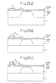
- Fig. 6 illustrates a conventional flow of steps generally employed, and Fig. 5 illustrates an electrode structure. That is, referring to Fig. 6, the aluminum wiring is formed after the circuit is formed, and the surface of the circuit is protected by the passivation film. Here, the passivation is opened to the aluminum wiring.
- a nickel film is plated by the non-electrolytic nickel plating on the aluminum wiring that is opened and gold is formed on nickel by non-electrolytic gold plating that is effected continuously.
- a diaphragm is formed in a state where the nickel/gold film 3 is plated on the aluminum wiring, and a glass substrate 2 and a silicon wafer 1 are anodically joined. Thereafter, the wafer is cut into chips.
- the diaphragm may be formed, the electrode may be formed and, then, the glass substrate may be joined causing, however, a problem in that silicon is exposed on the back surface of the wafer and the plated layer possesses an irregular thickness.
- a protection film resist film or the like film
- the gist of the invention resides in a semiconductor type sensor having, on a semiconductor substrate, a structural portion for detecting the physical quantity or the chemical component of a corrosive medium and an electric quantity conversion element, and having pads which are the output terminals for sending the detected electric signals to an external unit, wherein the pads are protected with a precious metal.
- the gist of the invention further resides in a method of producing a semiconductor type sensor comprising the steps of:
- the invention further has an object of providing a method of plating a semiconductor device best suited for the production of the semiconductor type sensor. That is, gold which is a precious metal having corrosion resistance is formed as a protection film on the conventional aluminum electrode, and an insulating film such as a gel protection film is formed thereon to decrease the probability of contact between the corrosive medium and aluminum, which forms a corrosive structure, in order to enhance the corrosion resistance of pads.
- the invention provides a method of plating a semiconductor device while maintaining a uniform thickness of the plated film, preventing the metal from being precipitated on the back surface of the semiconductor, preventing contamination in the subsequent steps and lowering the cost.
- the present invention is a method of plating a semiconductor device wherein in directly forming connection terminals on the aluminum electrodes on a semiconductor substrate, the non-electrolytic plating is effected in a state where the back surface of the substrate is covered with an insulator.
- a semiconductor type sensor has, in a semiconductor substrate such as wafer, a structural portion for detecting the physical quantity or the chemical component of a corrosive medium and an electric quantity conversion element, and has pads which are the output terminals for sending the detected electric signals to an external unit, wherein the pads are protected with a precious metal.
- the material forming pads is, preferably, aluminum.
- a glass substrate is arranged on the back surface of the semiconductor substrate.
- the precious metal used for protecting the pads in the present invention may be a single film of Au, Pt or Pd, or a composite film thereof.
- the precious metal is desirably obtained by non-electrolytically plating Ni/Au, Cu/Au, Ni/Pt or Ni/Pd and, particularly preferably, Ni/Au, successively, using a liquid not containing cyanide ions.
- the non-electrolytic plating is effected relying on the plating method of the invention that will be described later.
- Wires are bonded to the pads for sending the detected electric signals to an external unit.
- Gold is best suited as a wire material.
- the thus formed pads and wire-bonded portions are covered with an insulating film.
- the insulating film, material thereof and film thickness thereof may be those that have been widely used. For instance, there can be exemplified gel, primer + gel, or parylene + gel. As the gel, there can be exemplified fluorine gel, silicon gel or fluorosilicon gel.
- the electrode structure of the semiconductor type sensor of the present invention is produced by a method comprising the steps of:
- a semiconductor type sensor has, in a silicon semiconductor substrate, a structural portion for detecting the physical quantity and an electric quantity conversion element, and has pads, wherein the obtained electric signals are transmitted through wires. On the pads are formed nickel and gold films by the non-electrolytic plating, and the whole structure thereof is covered with a gel or other insulating film.
- a pressure sensor can be exemplified as a semiconductor type sensor for detecting the physical quantity of the corrosive medium. Particularly desirably, it is the pressure sensor for measuring the pressure of the exhaust gas in an exhaust gas environment of an automotive engine. Further, it is the pressure sensor for measuring the pressure of a medium which is highly corrosive and is highly humid.
- These pressure sensors have a thin diaphragm region formed in the semiconductor substrate in a customary manner, exhibit a piezo-resistance effect due to the diffusion layer formed in this region, and are so constituted that the distortion is converted into a change in the resistance to detect the pressure.
- the pads have a nickel layer formed by non-electrolytic plating maintaining a thickness of several microns on the aluminum layer of a thickness of 1.1 ⁇ m to assist the precipitation of gold. Then, gold of a thickness of about 0.2 ⁇ m is formed thereon non-electrolytically. Next, a gold wire is bonded (WB). This precludes most of the portions to where the corrosive solution comes in contact. However, a gap exists between the nickel film and the SiN film (chip protection film), and this portion is covered with an insulating film (gel/parylene/primer + gel).
- This production method has an advantage in that the plating portion is a completely self-forming process requiring neither a semiconductor step such as exposure to light/etching nor an aligner/clean room/coater developer which is an expensive facility.
- the working can be effected by treatment after the semiconductor step.
- the present invention prevents the corrosion of the signal transmission portions in the sensor that detects the physical quantities and chemical components of the corrosive medium, and contributes to extending the life of the product as compared to the conventional counterparts.
- the device when immersed in a strongly acidic aqueous solution of 90°C having a pH of about 1.7, the device offers a life which is about twice as long as that of the device of a structure in which aluminum is exposed.
- the non-electrolytic plating is effected in a state where the back surface of the substrate is covered with an insulator.
- the insulator is a glass substrate which is a part constituting the product.
- the glass substrate also serves as a material for covering the back surface of the substrate.
- the non-electrolytic plating treatment of the present invention is a non-electrolytic nickel plating.
- nickel is formed by the non-electrolytic nickel plating and, then, gold is formed by the non-electrolytic gold plating.
- These non-electrolytic nickel plating and non-electrolytic gold plating themselves can be carried out in a customary manner. According to the present invention, however, they are carried out after the glass substrate is joined as described above.
- the aluminum electrode is usually selected from any one of pure Al wiring, Al-Si wiring, Al-Cu wiring or Al-Si-Cu wiring.
- the pure Al wiring is usually the wiring of highly pure aluminum of a purity of not lower than 99.99% or not lower than 99.999%.
- silicon is contained, the amount of silicon is, usually, about 1%.
- the non-electrolytic nickel plating solution is, for example, a plating solution based on, for example, sodium hypophosphite or a boron compound.
- non-electrolytic nickel/gold plating zinc is substituted for the aluminum wiring by the zincate treatment, and nickel is precipitated by the non-electrolytic nickel plating. It is desired that the nickel plating solution contains hypophosphorous acid ions as a reducing agent. On the nickel plating, gold is desirably formed by the non-electrolytic plating to prevent the oxidation of nickel and to improve the junction to the wire that is bonded.
- the glass substrate may be covered with an insulator so that pores in the glass substrate will not be soaked with the non-electrolytic plating solution.
- the glass substrate can be covered with the insulator via an adhesive or a wax.
- the material that covers via the adhesive is desirably a resin or a glass.
- the adhesive or the wax may be applied to the outer circumference only of the glass so that the pores in the glass are little penetrated with the adhesive or the wax.
- the plating method of the present invention is best suited for the production of the semiconductor type sensors.
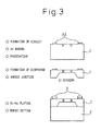
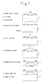
- Fig. 3 illustrates a flow of steps of the invention.
- an aluminum wiring is formed after a circuit is formed and, then, a passivation film is formed to protect the surface of the circuit.
- a diaphragm is formed to anodically join the glass substrate 2 and the silicon wafer 1 together.
- a nickel film is plated on the aluminum wiring by the non-electrolytic nickel plating and, then, gold is continuously formed on nickel by the non-electrolytic gold plating.
- the wafer is cut into chips.
- the electrode structure that is finally obtained becomes the same as that of the prior art illustrated in Fig. 5.
- the diaphragm is formed, the glass substrate is joined and, then, the electrode is formed (the electrode is formed or the non-electrolytic nickel/gold plating is effected in the final step) preventing the gold contamination in the subsequent steps.
- the glass substrate plays the role of the covering material to cover the back surface of the semiconductor substrate preventing the precipitation of metal on the back surface of the semiconductor substrate and enabling the plating to be uniformly accomplished.
- the present invention invention provides a semiconductor type sensor featuring improved corrosion resistance against a corrosive medium.
Landscapes
- Physics & Mathematics (AREA)
- General Physics & Mathematics (AREA)
- Fluid Mechanics (AREA)
- Microelectronics & Electronic Packaging (AREA)
- Analytical Chemistry (AREA)
- Toxicology (AREA)
- Engineering & Computer Science (AREA)
- Computer Hardware Design (AREA)
- Health & Medical Sciences (AREA)
- Chemical & Material Sciences (AREA)
- General Health & Medical Sciences (AREA)
- Pressure Sensors (AREA)
- Measuring Fluid Pressure (AREA)
- Electroplating Methods And Accessories (AREA)
- Chemically Coating (AREA)
- Electrodes Of Semiconductors (AREA)
- Internal Circuitry In Semiconductor Integrated Circuit Devices (AREA)
- Wire Bonding (AREA)
Applications Claiming Priority (3)
| Application Number | Priority Date | Filing Date | Title |
|---|---|---|---|
| JP2002371960 | 2002-12-24 | ||
| JP2002371960 | 2002-12-24 | ||
| PCT/JP2003/016625 WO2004059722A1 (ja) | 2002-12-24 | 2003-12-24 | 半導体式センサおよび半導体装置のめっき方法 |
Publications (2)
| Publication Number | Publication Date |
|---|---|
| EP1577936A1 true EP1577936A1 (de) | 2005-09-21 |
| EP1577936A4 EP1577936A4 (de) | 2006-03-15 |
Family
ID=32677219
Family Applications (1)
| Application Number | Title | Priority Date | Filing Date |
|---|---|---|---|
| EP03786283A Ceased EP1577936A4 (de) | 2002-12-24 | 2003-12-24 | Halbleitersensor und plattierungsverfahren für ein halbleiterbauelement |
Country Status (6)
| Country | Link |
|---|---|
| US (1) | US20050034526A1 (de) |
| EP (1) | EP1577936A4 (de) |
| JP (2) | JPWO2004059722A1 (de) |
| KR (1) | KR100646820B1 (de) |
| CN (2) | CN100527372C (de) |
| WO (1) | WO2004059722A1 (de) |
Cited By (1)
| Publication number | Priority date | Publication date | Assignee | Title |
|---|---|---|---|---|
| US8304847B2 (en) | 2005-11-01 | 2012-11-06 | Fuji Electric Co., Ltd. | Semiconductor pressure sensor |
Families Citing this family (12)
| Publication number | Priority date | Publication date | Assignee | Title |
|---|---|---|---|---|
| TWI280383B (en) * | 2004-06-29 | 2007-05-01 | Japan Ae Power Systems Corp | Partial discharge detecting sensor, and detecting device, and gas insulated electric apparatus provided with a partial discharge detecting sensor |
| JP2006030068A (ja) * | 2004-07-20 | 2006-02-02 | Denso Corp | 圧力センサ |
| JP2006226989A (ja) * | 2005-01-18 | 2006-08-31 | Denso Corp | 圧力センサの製造方法 |
| JP4507890B2 (ja) * | 2005-01-18 | 2010-07-21 | 株式会社デンソー | 圧力センサの製造方法 |
| CN100432645C (zh) * | 2005-01-18 | 2008-11-12 | 株式会社电装 | 制造压力传感器的方法 |
| JP2006200925A (ja) * | 2005-01-18 | 2006-08-03 | Denso Corp | 圧力センサ |
| US8394713B2 (en) * | 2010-02-12 | 2013-03-12 | Freescale Semiconductor, Inc. | Method of improving adhesion of bond pad over pad metallization with a neighboring passivation layer by depositing a palladium layer |
| JP5884921B2 (ja) | 2012-11-30 | 2016-03-15 | 富士電機株式会社 | 圧力センサ装置および圧力センサ装置の製造方法 |
| KR101808794B1 (ko) * | 2015-05-07 | 2018-01-18 | 주식회사 모다이노칩 | 적층체 소자 |
| EP3211394B1 (de) * | 2016-02-29 | 2021-03-31 | Melexis Technologies NV | Halbleiterdrucksensor für anwendung in rauen medien |
| JP6515944B2 (ja) * | 2016-12-20 | 2019-05-22 | 株式会社デンソー | 半導体装置およびその製造方法 |
| US10598559B2 (en) * | 2017-06-29 | 2020-03-24 | Rosemount Inc. | Pressure sensor assembly |
Family Cites Families (18)
| Publication number | Priority date | Publication date | Assignee | Title |
|---|---|---|---|---|
| JPS57136132A (en) * | 1981-02-18 | 1982-08-23 | Nippon Denso Co Ltd | Semiconductor pressure transducer |
| JPS62144368A (ja) * | 1985-12-19 | 1987-06-27 | Nec Corp | 半導体式圧力センサの保護膜 |
| JPH03101139A (ja) * | 1989-09-13 | 1991-04-25 | Seiko Epson Corp | 半導体素子の電極構造 |
| US5170237A (en) * | 1989-11-06 | 1992-12-08 | Matsushita Electronics Corporation | Semiconductor pressure sensor |
| JP3198779B2 (ja) * | 1994-03-04 | 2001-08-13 | 株式会社デンソー | 半導体圧力検出器の製造方法 |
| JP3555366B2 (ja) * | 1996-02-29 | 2004-08-18 | 松下電工株式会社 | 圧力センサの製造方法 |
| JPH10153508A (ja) * | 1996-11-26 | 1998-06-09 | Fuji Electric Co Ltd | 半導体圧力センサ |
| JPH1123613A (ja) * | 1997-07-04 | 1999-01-29 | Tokai Rika Co Ltd | ダイアフラム式センサチップを利用したセンサ |
| US5955771A (en) * | 1997-11-12 | 1999-09-21 | Kulite Semiconductor Products, Inc. | Sensors for use in high vibrational applications and methods for fabricating same |
| JP3398609B2 (ja) * | 1998-11-30 | 2003-04-21 | シャープ株式会社 | 半導体装置 |
| JP2000232078A (ja) * | 1999-02-10 | 2000-08-22 | Toshiba Corp | メッキ方法及びメッキ装置 |
| US6260417B1 (en) * | 1999-10-13 | 2001-07-17 | Denso Corporation | Semiconductor pressure sensor device with multi-layered protective member that reduces void formation |
| JP3591425B2 (ja) * | 2000-04-27 | 2004-11-17 | 株式会社デンソー | 圧力センサ |
| FR2812969B1 (fr) * | 2000-08-11 | 2003-08-01 | Thomson Csf | Capteur micro-usine avec soudure electrolytique et procede de fabrication |
| FR2812968B1 (fr) * | 2000-08-11 | 2003-08-01 | Thomson Csf | Capteur micro-usine avec protection isolante des connexions |
| JP3679001B2 (ja) * | 2000-12-22 | 2005-08-03 | シャープ株式会社 | 半導体装置およびその製造方法 |
| US7057247B2 (en) * | 2001-12-12 | 2006-06-06 | Kulite Semiconductor Products, Inc. | Combined absolute differential transducer |
| JP2003247903A (ja) * | 2002-02-21 | 2003-09-05 | Denso Corp | 圧力センサ |
-
2003
- 2003-12-24 WO PCT/JP2003/016625 patent/WO2004059722A1/ja not_active Ceased
- 2003-12-24 EP EP03786283A patent/EP1577936A4/de not_active Ceased
- 2003-12-24 KR KR1020047014152A patent/KR100646820B1/ko not_active Expired - Fee Related
- 2003-12-24 CN CNB2003801003346A patent/CN100527372C/zh not_active Expired - Fee Related
- 2003-12-24 CN CN2007101668208A patent/CN101145532B/zh not_active Expired - Fee Related
- 2003-12-24 JP JP2004562923A patent/JPWO2004059722A1/ja active Pending
-
2004
- 2004-09-28 US US10/950,561 patent/US20050034526A1/en not_active Abandoned
-
2010
- 2010-01-12 JP JP2010004134A patent/JP5056862B2/ja not_active Expired - Fee Related
Cited By (1)
| Publication number | Priority date | Publication date | Assignee | Title |
|---|---|---|---|---|
| US8304847B2 (en) | 2005-11-01 | 2012-11-06 | Fuji Electric Co., Ltd. | Semiconductor pressure sensor |
Also Published As
| Publication number | Publication date |
|---|---|
| CN101145532A (zh) | 2008-03-19 |
| CN1692484A (zh) | 2005-11-02 |
| KR20050002850A (ko) | 2005-01-10 |
| JP5056862B2 (ja) | 2012-10-24 |
| KR100646820B1 (ko) | 2006-11-23 |
| CN101145532B (zh) | 2010-06-02 |
| CN100527372C (zh) | 2009-08-12 |
| WO2004059722A1 (ja) | 2004-07-15 |
| JPWO2004059722A1 (ja) | 2006-05-11 |
| EP1577936A4 (de) | 2006-03-15 |
| US20050034526A1 (en) | 2005-02-17 |
| JP2010135811A (ja) | 2010-06-17 |
Similar Documents
| Publication | Publication Date | Title |
|---|---|---|
| JP5056862B2 (ja) | 半導体式センサの製造方法 | |
| US7078796B2 (en) | Corrosion-resistant copper bond pad and integrated device | |
| US7530276B2 (en) | Semiconductor pressure sensor and manufacturing method thereof | |
| EP1947439B1 (de) | Halbleiter-drucksensor | |
| US7855103B2 (en) | Wirebond structure and method to connect to a microelectronic die | |
| US20050104207A1 (en) | Corrosion-resistant bond pad and integrated device | |
| JP3398609B2 (ja) | 半導体装置 | |
| EP0736757A1 (de) | Korrosionsbeständige Mikrosensorstruktur durch anorganischen Überzug | |
| CN107525620B (zh) | 用于恶劣媒介应用的半导体传感器组装件 | |
| JPH0474432A (ja) | 半導体装置及びその製造方法 | |
| US20060107750A1 (en) | Pressure sensor and manufacturing method of the same | |
| US7036384B2 (en) | Pressure sensor | |
| JP2009294044A (ja) | 半導体装置の製造方法 | |
| CN100432645C (zh) | 制造压力传感器的方法 | |
| JP4507890B2 (ja) | 圧力センサの製造方法 | |
| JP4927357B2 (ja) | 圧力センサおよびその製造方法 | |
| JP2007067398A (ja) | 過酷な化学的、熱的環境に晒される半導体をベースにした圧力センサー用メタルコンタクトシステム | |
| US20060160263A1 (en) | Method for manufacturing pressure sensor | |
| JP3435369B2 (ja) | 半導体デバイス | |
| EP0730296A2 (de) | Leiterrahmen für plastikumhüllte Halbleiteranordnung, Halbleiteranordnung unter Verwendung desselben und Herstellungsverfahren für einen Leiterrahmen | |
| JPS60195961A (ja) | 半導体装置 | |
| CN1612335A (zh) | 改进的半导体导线架 |
Legal Events
| Date | Code | Title | Description |
|---|---|---|---|
| PUAI | Public reference made under article 153(3) epc to a published international application that has entered the european phase |
Free format text: ORIGINAL CODE: 0009012 |
|
| 17P | Request for examination filed |
Effective date: 20040823 |
|
| AK | Designated contracting states |
Kind code of ref document: A1 Designated state(s): AT BE BG CH CY CZ DE DK EE ES FI FR GB GR HU IE IT LI LU MC NL PT RO SE SI SK TR |
|
| RIN1 | Information on inventor provided before grant (corrected) |
Inventor name: KONDO, ICHIHARU,C/O NTELLECTUAL PROPERTY CENTER Inventor name: SHINYAMA, KEIJI,C/O NTELLECTUAL PROPERTY CENTER Inventor name: WATANABE, YOSHIFUMI,C/O NTELLECTUAL PROP. CENTER Inventor name: TANAKA, HIROAKI,C/O INTELLECTUAL PROPERTY CENTER Inventor name: ABE, YOSITUGU,C/O NTELLECTUAL PROPERTY CENTER Inventor name: TOYODA, INAO,C/O INTELLECTUAL PROPERTY CENTER |
|
| A4 | Supplementary search report drawn up and despatched |
Effective date: 20060127 |
|
| RIC1 | Information provided on ipc code assigned before grant |
Ipc: G01L 9/00 20060101AFI20060123BHEP Ipc: H01L 23/485 20060101ALI20060123BHEP Ipc: H01L 29/84 20060101ALI20060123BHEP |
|
| 17Q | First examination report despatched |
Effective date: 20061030 |
|
| REG | Reference to a national code |
Ref country code: DE Ref legal event code: R003 |
|
| STAA | Information on the status of an ep patent application or granted ep patent |
Free format text: STATUS: THE APPLICATION HAS BEEN REFUSED |
|
| 18R | Application refused |
Effective date: 20160828 |