EP1947439B1 - Halbleiter-drucksensor - Google Patents
Halbleiter-drucksensor Download PDFInfo
- Publication number
- EP1947439B1 EP1947439B1 EP05800425A EP05800425A EP1947439B1 EP 1947439 B1 EP1947439 B1 EP 1947439B1 EP 05800425 A EP05800425 A EP 05800425A EP 05800425 A EP05800425 A EP 05800425A EP 1947439 B1 EP1947439 B1 EP 1947439B1
- Authority
- EP
- European Patent Office
- Prior art keywords
- gold
- pressure sensor
- layer
- pads
- diffusion
- Prior art date
- Legal status (The legal status is an assumption and is not a legal conclusion. Google has not performed a legal analysis and makes no representation as to the accuracy of the status listed.)
- Expired - Lifetime
Links
Images


Classifications
-
- G—PHYSICS
- G01—MEASURING; TESTING
- G01L—MEASURING FORCE, STRESS, TORQUE, WORK, MECHANICAL POWER, MECHANICAL EFFICIENCY, OR FLUID PRESSURE
- G01L15/00—Devices or apparatus for measuring two or more fluid pressure values simultaneously
-
- G—PHYSICS
- G01—MEASURING; TESTING
- G01L—MEASURING FORCE, STRESS, TORQUE, WORK, MECHANICAL POWER, MECHANICAL EFFICIENCY, OR FLUID PRESSURE
- G01L19/00—Details of, or accessories for, apparatus for measuring steady or quasi-steady pressure of a fluent medium insofar as such details or accessories are not special to particular types of pressure gauges
- G01L19/0007—Fluidic connecting means
- G01L19/0038—Fluidic connecting means being part of the housing
-
- G—PHYSICS
- G01—MEASURING; TESTING
- G01L—MEASURING FORCE, STRESS, TORQUE, WORK, MECHANICAL POWER, MECHANICAL EFFICIENCY, OR FLUID PRESSURE
- G01L19/00—Details of, or accessories for, apparatus for measuring steady or quasi-steady pressure of a fluent medium insofar as such details or accessories are not special to particular types of pressure gauges
- G01L19/0061—Electrical connection means
- G01L19/0084—Electrical connection means to the outside of the housing
-
- G—PHYSICS
- G01—MEASURING; TESTING
- G01L—MEASURING FORCE, STRESS, TORQUE, WORK, MECHANICAL POWER, MECHANICAL EFFICIENCY, OR FLUID PRESSURE
- G01L19/00—Details of, or accessories for, apparatus for measuring steady or quasi-steady pressure of a fluent medium insofar as such details or accessories are not special to particular types of pressure gauges
- G01L19/06—Means for preventing overload or deleterious influence of the measured medium on the measuring device or vice versa
- G01L19/0627—Protection against aggressive medium in general
-
- G—PHYSICS
- G01—MEASURING; TESTING
- G01L—MEASURING FORCE, STRESS, TORQUE, WORK, MECHANICAL POWER, MECHANICAL EFFICIENCY, OR FLUID PRESSURE
- G01L19/00—Details of, or accessories for, apparatus for measuring steady or quasi-steady pressure of a fluent medium insofar as such details or accessories are not special to particular types of pressure gauges
- G01L19/14—Housings
- G01L19/141—Monolithic housings, e.g. molded or one-piece housings
-
- G—PHYSICS
- G01—MEASURING; TESTING
- G01L—MEASURING FORCE, STRESS, TORQUE, WORK, MECHANICAL POWER, MECHANICAL EFFICIENCY, OR FLUID PRESSURE
- G01L19/00—Details of, or accessories for, apparatus for measuring steady or quasi-steady pressure of a fluent medium insofar as such details or accessories are not special to particular types of pressure gauges
- G01L19/14—Housings
- G01L19/147—Details about the mounting of the sensor to support or covering means
-
- H—ELECTRICITY
- H10—SEMICONDUCTOR DEVICES; ELECTRIC SOLID-STATE DEVICES NOT OTHERWISE PROVIDED FOR
- H10W—GENERIC PACKAGES, INTERCONNECTIONS, CONNECTORS OR OTHER CONSTRUCTIONAL DETAILS OF DEVICES COVERED BY CLASS H10
- H10W72/00—Interconnections or connectors in packages
- H10W72/50—Bond wires
- H10W72/531—Shapes of wire connectors
- H10W72/536—Shapes of wire connectors the connected ends being ball-shaped
-
- H—ELECTRICITY
- H10—SEMICONDUCTOR DEVICES; ELECTRIC SOLID-STATE DEVICES NOT OTHERWISE PROVIDED FOR
- H10W—GENERIC PACKAGES, INTERCONNECTIONS, CONNECTORS OR OTHER CONSTRUCTIONAL DETAILS OF DEVICES COVERED BY CLASS H10
- H10W72/00—Interconnections or connectors in packages
- H10W72/50—Bond wires
- H10W72/531—Shapes of wire connectors
- H10W72/5363—Shapes of wire connectors the connected ends being wedge-shaped
-
- H—ELECTRICITY
- H10—SEMICONDUCTOR DEVICES; ELECTRIC SOLID-STATE DEVICES NOT OTHERWISE PROVIDED FOR
- H10W—GENERIC PACKAGES, INTERCONNECTIONS, CONNECTORS OR OTHER CONSTRUCTIONAL DETAILS OF DEVICES COVERED BY CLASS H10
- H10W72/00—Interconnections or connectors in packages
- H10W72/50—Bond wires
- H10W72/551—Materials of bond wires
- H10W72/552—Materials of bond wires comprising metals or metalloids, e.g. silver
- H10W72/5522—Materials of bond wires comprising metals or metalloids, e.g. silver comprising gold [Au]
-
- H—ELECTRICITY
- H10—SEMICONDUCTOR DEVICES; ELECTRIC SOLID-STATE DEVICES NOT OTHERWISE PROVIDED FOR
- H10W—GENERIC PACKAGES, INTERCONNECTIONS, CONNECTORS OR OTHER CONSTRUCTIONAL DETAILS OF DEVICES COVERED BY CLASS H10
- H10W72/00—Interconnections or connectors in packages
- H10W72/50—Bond wires
- H10W72/551—Materials of bond wires
- H10W72/552—Materials of bond wires comprising metals or metalloids, e.g. silver
- H10W72/5524—Materials of bond wires comprising metals or metalloids, e.g. silver comprising aluminium [Al]
-
- H—ELECTRICITY
- H10—SEMICONDUCTOR DEVICES; ELECTRIC SOLID-STATE DEVICES NOT OTHERWISE PROVIDED FOR
- H10W—GENERIC PACKAGES, INTERCONNECTIONS, CONNECTORS OR OTHER CONSTRUCTIONAL DETAILS OF DEVICES COVERED BY CLASS H10
- H10W72/00—Interconnections or connectors in packages
- H10W72/90—Bond pads, in general
- H10W72/931—Shapes of bond pads
- H10W72/932—Plan-view shape, i.e. in top view
Definitions
- the present invention relates to a mounting structure for a semiconductor pressure sensor that uses semiconductor strain gages to improve corrosion resistance to corrosive gases.
- a semiconductor pressure sensor using semiconductor a strain gage has been used for measurement of an intake air pressure in an automobile and others.
- the adoption of EGR for recirculating exhaust gas to an intake air system has been spread and a recirculation rate of EGR tends to increase particularly in an application to a diesel engine.
- a semiconductor pressure sensor for pressure measurement on the intake air system with EGR has been used in an environment where the semiconductor pressure sensor is more likely to be exposed in exhaust gas, the necessity of resistance to exhaust gas is increasing.
- DPF Diesel Particulate Filter
- PMs particulate matters
- a pressure sensitive element of a pressure sensor for use the clogging detection is required to have resistance to exhaust gas.
- Patent Document 1 a Ti coating film and a Pd coating film are used as a measure for preventing the corrosion of the aluminum electrode.
- Such a measure is particularly aimed at improving corrosion resistance of the aluminum electrode against humidity and moisture.
- the measure is still insufficient for the resistance of corrosion caused by nitrate ions in nitrogen oxide contained in exhaust gas.
- Patent Document 1 JP-A No. 153508/1998
- EP 1 577 936 A1 discloses a semiconductor type pressure sensor comprising aluminium electrodes as wiring pads. On the aluminium electrodes a nickel (Ni) layer and a gold (Au) layer are formed. The gold layer serves to improve the corrosion resistance of the aluminium layer against a corrosive medium.
- the nickel layer is formed by non-electrolytic plating on the aluminium electrode and assists the precipitation of gold.
- US 2005/001316A1 discloses an integrated device with a corrosion-resistant bond pad comprising at least one aluminium bond pad on a semiconductor substrate, a layer of nickel disposed on the aluminium bond pad, a layer of palladium disposed on the nickel layer, and a layer of gold disposed on the palladium layer.
- the aluminium bond pad is passivated and protected without requiring an encapsulation material, such as a silicone.
- EP 0 567 937 A2 discloses a semiconductor chip including several bonding pads. Each bonding pad comprises in this order an aluminium electrode, a layer made of titanium-tungsten and a layer made of gold on top which serves for attaching gold bond wires.
- the function of the titanium-tungsten layer between the aluminium electrode and the gold layer is to avoid the so-called "purple plague", which is a chemical reaction between aluminium and gold at temperatures over 125 °C.
- US 5,942,448 discloses an integrated circuit comprising a layer of aluminium, a layer of titanium-tungsten and a layer of gold in this order.
- US 5,942,448 discloses an etchant for etching integrated circuits having the above described Al/TiW/Au layer structure.
- a conventional semiconductor pressure sensor uses aluminum electrodes at bonding pads functioning as electrical input and output terminals of a semiconductor strain gage chip, external input and output terminals (usually nickel-plated terminals) to input and output signals of the gage, and aluminum wires to connect the aluminum electrodes to the external input and output terminals respectively by bonding.
- a problem of such a mounting structure for these elements of the semiconductor pressure sensor is that, when it is used in an environment containing exhaust gas for a long period of time, the aluminum wire may be corroded by nitrate ions produced from nitrogen oxide contained in the exhaust gas.
- An object of the present invention is, in view of the above problem in the conventional technology, to provide a semiconductor pressure sensor having a sufficiently high corrosion resistance even in an exhaust gas environment.
- Other objects of the present invention will be elaborated in the explanations on the following embodiments.
- the present invention to attain the above objects is a pressure sensor to measure a pressure of a gas containing corrosive components such as exhaust gas and is characterized in that: the whole area of a semiconductor chip, except for pads for wire bonding and probe pads for characteristic confirmatory checkwhich function as electrical input and output portions, is coated with a corrosion-resistant material such as silicon nitride (SiN); an adhesion ensuring-diffusion preventative layer is formed on aluminum electrodes at the pads for wire bonding and the probe pads for characteristic confirmatory check; and the surface of the adhesion ensuring-diffusion preventative layer is coated with gold.
- a corrosion-resistant material such as silicon nitride (SiN)
- SiN silicon nitride
- an adhesion ensuring-diffusion preventative layer is formed on aluminum electrodes at the pads for wire bonding and the probe pads for characteristic confirmatory check
- the surface of the adhesion ensuring-diffusion preventative layer is coated with gold.
- the adhesion ensuring-diffusion preventative layer is, for example, formed by sputtering, vapor deposition, or plating of titanium-tungsten (TiW)
- the adhesion ensuring-diffusion preventative layer has, for example, a thickness of about 0.25 ⁇ m and is configured so as to overhang the silicon nitride.
- the electrical input and output portions of the semiconductor chip are, for example, connected to the external input and output terminals with gold wires respectively and the surfaces of the external input and output terminals are coated with gold.
- the thickness of the gold coating is, for example, not less than 0.5 ⁇ m.
- the semiconductor chip is, for example, bonded to glass with anodic bonding and the temperature in the anodic bonding is not higher than 320°C.
- the surface of the adhesion ensuring-diffusion preventative layer is, for example, formed at the pads for wire bonding and the probe pads for characteristic confirmatory check are coated with gold after the semiconductor chip bonded to glass with anodic bonding.
- the semiconductor pressure sensor is, for example, configured so that parts of aluminum of the lower portions of the aluminum electrodes to which wire bonding is applied may be cut out in order to prevent the adhesion ensuring-diffusion preventative layer from being damaged due to the application of vibration at the gold coating.
- the pads for wire bonding and the probe pads for characteristic confirmatory check are provided with the adhesion ensuring-diffusion preventive layer in an aluminum wiring layout and hence the gold coating applied on the outermost surface of the pads is prevented from diffusing into the aluminum electrodes. Further, since the electrical input and output portions of the semiconductor chip are connected to the exterior input and output terminals with the gold wires and the gold has the smallest ionization tendency in metallic elements, it is possible to prevent corrosion caused by corrosive matters.
- the whole area of a semiconductor chip except for pads for wire bonding and probe pads for characteristic confirmatory check which are functions as electrical input and output portions, is coated with a corrosion-resistant material such as silicon nitride (SiN).
- a corrosion-resistant material such as silicon nitride (SiN).
- the pads for wire bonding and the probe pads for characteristic confirmatory check are provided with the adhesion ensuring-diffusion preventive layer in an aluminum wiring layout.
- the outermost surface of the layer is coated with gold.
- the adhesion ensuring-diffusion preventative layer in the aluminum wiring layout is formed by sputtering, vapor deposition, or plating of titanium-tungsten (TiW). By so doing, it is possible to prevent gold coating applied to the outermost surfaces of the layer from diffusing into the aluminum electrodes.
- electrical input and output portions of the semiconductor chip are connected to external input and output terminals for the electrical I/O of the semiconductor chip with gold wires and the surfaces of the external input and output terminals are coated with gold by plating or the like.
- the gold coating on the outermost surfaces of the pads for wire bonding and the probe pads for characteristic confirmatory check as electrical I/O portions on the surface of the semiconductor chip is formed by sputtering, plating, or both sputtering and plating.
- the thickness of the gold coating is not less than 0.5 micrometer and thereby the corrosion resistance is ensured.
- the semiconductor chip When a semiconductor strain gage is mounted as a semiconductor pressure sensor, the semiconductor chip is required to have good handleability. Further, in the case of an absolute pressure sensor, the semiconductor chip is bonded to a glass substrate with anodic bonding in order to form a vacuum chamber.
- the temperature at the anodic bonding is 320°C or lower. If bonding is applied at a temperature higher than 320°C, cracks may be formed in the adhesion ensuring-diffusion preventative layer because of the difference in linear expansion coefficient among the aluminum electrodes, the adhesion ensuring-diffusion preventative layer, and the gold-coated layers, and accordingly gold may diffuse into aluminum.
- the adhesion ensuring-diffusion preventative layer is formed on the pads for wire bonding and the probe pads for characteristic confirmatory check as the electrical I/O portions on the semiconductor chip surface and gold coating is applied.
- adhesion ensuring-diffusion preventative layer is formed on the pads for wire bonding and probe pads for characteristic confirmation in aluminum wire layout and hence the gold coating applied on the outermost surfaces of the layer is prevented from diffusing into the aluminum electrodes. If the layer are not formed, gold diffuses into aluminum and improvement in the corrosion resistance of the connected electrodes can not be ensured by gold coating.
- the electrical input and output portions in the semiconductor chip are connected to the external input and output terminals with gold wires.
- the gold coating on the outermost surfaces of the pads for wire bonding and the probe pads for characteristic confirmatory check can be formed by sputtering, plating, or both sputtering and plating and thus can be formed in a usually used process for forming a gold bump in a semiconductor.
- the corrosion resistance is secured by setting the thickness of the gold-coated layer at not less than 5 micrometer. When the thickness is less than 5 micrometer, corrosion proceeds due to corrosive matters and an intended service life cannot be obtained.
- the temperature at which the semiconductor chip is anodically bonded to the glass substrate in order to form a vacuum chamber is 320°C or lower. If bonding is applied at a temperature higher than 320°C, cracks are formed in the adhesion ensuring-diffusion preventative layer because of the difference in linear expansion coefficient among these layers, gold diffuses into aluminum, and the surfaces of the electrodes cannot be coated with gold. Consequently, not only corrosion resistance cannot be secured but also gold wire bonding cannot be applied.
- the adhesion ensuring-diffusion preventive layer at the pads for wire bonding and the probe pads and applying gold coating after the semiconductor chip is anodically bonded to the glass substrate, the cracks are prevented from occurring in the adhesion ensuring-diffusion preventative layer due to the heating at the anodic bonding and gold is prevented from diffusing into the aluminum electrodes. By so doing, the corrosion resistance of the gold-coated electrodes is ensured.
- the adhesion ensuring-diffusion preventing layer is prevented from being damaged by vibration caused by the application of load at the gold wire bonding and gold is prevented from diffusing into the aluminum electrodes.
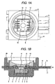
- Fig. 1 comprises a front view ( Fig. 1(A) ) and a sectional view ( Fig. 1(B) ) showing a semiconductor pressure sensor submodule according to the first embodiment of the present invention.
- the present embodiment is the case where a pressure sensitive element of the pressure sensor is formed with a small submodule.
- a diaphragm 1 made of silicon and provided with resistances (not shown in the figure) functioning as a strain gage are formed in a sensor chip 2.
- the strain gage-resistances and aluminum electrodes 3 to connect them are formed on the surface of the sensor chip 2.
- the sensor chip 2 is covered with silicon nitride (SiN) 4 in order to protect the strain gage-resistances and the aluminum electrodes against a corrosive environment.
- the aluminum electrodes are exposed usually and the signal are output to the exterior through aluminum wires or gold wires.
- Each of wire bonding pads according to the present embodiment is configured by forming an adhesion ensuring-diffusion preventative layer (hereunder referred to as a titanium-tungsten layer) 5 made of titanium-tungsten (TiW) on an aluminum electrode 3, and furthermore forming a gold electrode 6 thereon by goldplating.
- the thickness of the gold-plated layer is not less than 0.5 ⁇ m.
- the adhesion ensuring-diffusion preventative layer can be formed, besides by sputtering, by vapor deposition or plating.
- sputtering by vapor deposition or plating.
- NOx nitrogen oxide
- each of probe pads for characteristic confirmatory check is configured by forming a titanium-tungsten layer 5 on an aluminum electrode and forming a gold electrode thereon by gold plating; and confirms characteristics by probing with the gold electrode.
- the sensor chip 2 is mounted on a glass substrate 7 by anodic bonding.
- the anodic bonding is applied at a high temperature.
- the phenomena observed when anodic bonding is applied at a high temperature of 320°C or higher are that: cracks occur in the titanium-tungsten layer 5; gold in the gold electrode 6 diffuses into the aluminum electrode 3; and the gold protective layer disappears.
- the sensor chip 2 is mounted on the glass substrate 7 and the glass substrate 7 is bonded to a case 8 of the submodule with an adhesive agent 9.
- Terminals 10 for inputting and outputting signals from the submodule to the exterior are provided in the case 8 by insert molding.
- the terminals 10 are formed by coating a base material 11 with a nickel plated layer 12 and thereafter with a gold plated layer 13.
- the terminals' portions connected to the sensor chip 2 are exposed to a corrosive environment in the same way as the sensor chip 2 and hence the corrosion resistance is enhanced with the gold plated layer 13.
- fluorine-type gel 15 is provided in the case 8 to cover the sensor chip 2 and the gold wires 14 in the present embodiment.
- the whole upper surface of the gel 15 is used as a pressure receiving portion.
- Fig. 2 is an enlarged sectional view showing a substantial part of the pressure sensor submodule shown in Fig. 1 .
- the titanium-tungsten layer 5 is formed on an aluminum electrode 3 so as to overhang the silicon nitride 4 by sputtering or the like.
- the thickness of the titanium-tungsten layer 5 is about 0.25 ⁇ m. It is intended so that corrosive matters may hardly reach the aluminum electrode 3 through the interface between the silicon nitride 4 and the titanium-tungsten layer 5. Further, goldplating is applied on the titanium-tungsten layer 5 and thus a gold electrode 6 covered entirely with gold is formed.
- each of the terminals 10 is coated with a nickel-plated layer 12 and thereafter a gold-plated layer 13.
- Fig. 3 is a sectional view showing a pressure sensor when a pressure sensor submodule is mounted on a housing.
- the pressure sensor submodule 20 shown in Fig. 1 is mounted to a housing 23 with a connector 21 for electrical I/O to the exterior, a pressure inlet 22 to introduce the pressure of a measured pressure medium.
- each of terminals 10 of the submodule 20 is connected to a connector terminal 24 by welding. Further, the submodule 20 is fixed with epoxy resin 25 and the epoxy resin 25 has also the function as a sealant to prevent leakage of pressure or the like from the pressure inlet 22.
- Exhaust gas or the like as a measured medium reaches the interior of the sensor through the pressure inlet 22 and the pressure deforms a diaphragm 1 of the sensor chip 2 through the gel 15.
- the deformation of the diaphragm 1 causes the pressure to convert into an electric signal due to the resistance change of strain gages (not shown in the figure) attached to the diaphragm 1 and the electric signal is transferred to the exterior through the bonding wires 14, the terminals 10, and the connectors 24.
- corrosive matters are prevented from reaching underneath layers of the gage chip by covering the parts with the silicon nitride 4 which is coated over the whole of gage chip except for the electrical I/O portions.
- the titanium-tungsten layers 5 and the gold electrodes 6 are applied on the aluminum electrodes 3 as stated above.
- the bonding wires through which signals from the electrodes 3 are input and output are also prevented from corroding by using the gold wires 14.
- each of the terminals is also prevented from corroding by applying the gold-plated layers 13 on the surfaces of the submodule terminals 11.
- Fig. 4 shows a structure of a differential pressure sensor that is an example to which the present invention is applied.
- the present differential pressure sensor is configured by using two pieces of pressure sensor submodules 20 for absolute pressure measurement. It outputs the differential pressure signals that represent the difference between the signals from the two sensors on the circuit board.
- DPF Diesel Particulate Filter
- PMs particulate matters
- pressure is measured by using two pieces of pressure sensor submodules 20 comprising gold electrodes, gold wires and gold-plated terminals and measuring absolute pressure, the signals from the pressure sensor submodules 20 are processed on a circuit board 33, and thereby differential pressure signals are output.
- the pressures on both of upstream from and downstream from the filter are introduced into the pressure inlets 31 and 32 of the differential pressure sensor respectively.
- the pressure sensor submodules 20 mounted in the pressure inlets convert the pressures into electric signals.
- the pressure signals from the submodules 20 are taken into the substrate 33 and the differential signals are processed from the signals of the pressure sensor submodules 20 and output in a differential pressure signal processing circuit installed on the circuit board.
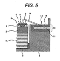
- Fig. 5 is an enlarged sectional view showing a partially modified substantial part of the pressure sensor submodule shown in Fig. 2 .
- a gold electrode 6 of a sensor chip 2 is electrically connected to the gold-plated layer 13 of a terminal 10 with a gold wire 14 by wire bonding.
- the gold wire 14 for bonding, corrosion resistance against corrosive matters is improved.
- parts of an aluminum electrode immediately under the part subjected to the wire bonding are cut out locally. By so doing, a titanium-tungsten layer 5 is prevented from incurring cracks when load and vibration are applied due to the bonding and the gold in the gold electrode 6 is prevented from diffusing into the aluminum electrode 3.
- the shape of the aluminum electrode after locally cut may be changed variously besides the case shown in Fig. 5 . Further, the aluminum electrode may have a structure wherein the part thereof immediately under the portion bonded beforehand is cut out.
- an aluminum electrode used as an electrode chip of a semiconductor pressure sensor is susceptible to a corrosive environment and a measure against the corrosion is necessary when it is used in a corrosive environment.
- the present invention proposes a corrosion-resistant structure of a semiconductor pressure sensor used in such a corrosive environment and the practical application thereof is expected.
Landscapes
- Physics & Mathematics (AREA)
- General Physics & Mathematics (AREA)
- Chemical & Material Sciences (AREA)
- Analytical Chemistry (AREA)
- Measuring Fluid Pressure (AREA)
- Pressure Sensors (AREA)
- Wire Bonding (AREA)
Claims (9)
- Halbleiterdrucksensor für eine Verwendung in einer Abgasumgebung eines Kraftfahrzeugverbrennungsmotors zum Messen des Drucks in einem korrosive Komponenten enthaltenden Abgas, wobei der Sensor Folgendes aufweist:- einen Halbleiterchip (2),- Kontaktstellen zum Drahtbonden und Prüfkontaktstellen (16) für charakteristische Überprüfungskontrollen an der Oberfläche des Halbleiterchips (2), wobei die Kontaktstellen Aluminiumelektroden (3) umfassen und als elektrische Eingabe- und Ausgabebereiche fungieren,- eine korrosionsbeständiges Material (4), wie beispielsweise Siliciumnitrid (SiN), das, mit Ausnahme der Kontaktstellen zum Drahtbonden und der Prüfkontaktstellen (16) für charakteristische Überprüfungskontrollen, eine BeschiChtung der gesamten Oberfläche des Halbleiterchips (2) ausbildet, und- eine haftvermittelnde und diffusionsverhindernde Schicht (5), die an den Aluminiumelektroden (3) der Kontaktstellen zum Drahtbonden und der Prüfkontaktstellen (16) für charakteristische Überprüfungskontrollen ausgebildet ist; wobei die Oberfläche der haftvermittelnden und diffusionsverhindernden Schicht (5) mit Gold (6) beschichtet ist,dadurch gekennzeichnet, dass Titan-Wolfram (TiW) die haftvermittelnde und diffusionsverhindernde Schicht (5) bildet.
- Halbleiterdrucksensor nach Anspruch 1, worin die Haftschicht durch Kathodenzerstäuben, Dampfphasenabscheiden oder Beschichten mit Titan-Wolfram (TiW) gebildet ist.
- Halbleiterdrucksensor nach Anspruch 1 oder 2, worin das korrosionsbeständige Material (4) aus Siliciumnitrid besteht und worin die haftvermittelnde, diffusionsverhindernde Schicht (5) eine Dicke von etwa 0,25 µm aufweist und so ausgebildet ist, dass sie über das Siliciumnitrid (4) hervorsteht.
- Halbleiterdrucksensor nach einem der Ansprüche bis 3, worin die Eingabe- und Ausgabebereiche des Halbleiterchips (2) jeweils über Golddrähte (14) mit externen Eingabe- und Ausgabeanschlüssen (10) verbunden und die Oberflächen der externen Eingabe- und Ausgabeanschlüssen (10) mit Gold (13) beschichtet sind.
- Halbleiterdrucksensor nach einem der Ansprüche 1 bis 3, worin die Goldbeschichtung (6) an den Oberflächen der Kontaktstellen zum Drahtbonden und der Prüfkontaktstellen (16) für charakteristische Überprüfungskontrollen durch Kathodenzerstäuben, Beschichten oder sowohl Kathodenzerstäuben als auch Beschichten gebildet sind.
- Halbleiterdrucksensor nach Anspruch 5, worin die Dicke der Goldbeschichtung (6) nicht weniger als 0,5 µm beträgt.
- Halbleiterdrucksensor nach einem der Ansprüche 1 bis 6, worin der Halbleiterchip (2) mittels anodischem Bonden auf einem Glas (7) befestigt und die Temperatur beim anodischen Bonden nicht höher als 320 °C ist.
- Halbleiterdrucksensor nach einem der Ansprüche 1 bis 6, worin die Beschichtung der Oberfläche der haftvermittelnden und diffusionsverhindernden Schicht (5) mit Gold (6) nach dem Befestigen des Halbleiterchips (2) an dem Glas (7) erfolgte.
- Halbleiterdrucksensor nach einem der Ansprüche 1 bis 6, worin der Halbleiterdrucksensor so ausgebildet ist, dass Teile des Aluminiums an den unteren Bereichen der Aluminiumelektroden (3), an denen das Drahtbonden erfolgt, ausgeschnitten sein können, um ein Beschädigen der haftvermittelnden und diffusionsverhindernden Schicht (5) infolge von auf die Goldbeschichtung (6) einwirkender Vibration zu vermeiden.
Applications Claiming Priority (1)
| Application Number | Priority Date | Filing Date | Title |
|---|---|---|---|
| PCT/JP2005/020072 WO2007052335A1 (ja) | 2005-11-01 | 2005-11-01 | 半導体圧力センサ |
Publications (3)
| Publication Number | Publication Date |
|---|---|
| EP1947439A1 EP1947439A1 (de) | 2008-07-23 |
| EP1947439A4 EP1947439A4 (de) | 2009-07-01 |
| EP1947439B1 true EP1947439B1 (de) | 2012-02-08 |
Family
ID=38005499
Family Applications (1)
| Application Number | Title | Priority Date | Filing Date |
|---|---|---|---|
| EP05800425A Expired - Lifetime EP1947439B1 (de) | 2005-11-01 | 2005-11-01 | Halbleiter-drucksensor |
Country Status (5)
| Country | Link |
|---|---|
| US (1) | US8304847B2 (de) |
| EP (1) | EP1947439B1 (de) |
| JP (1) | JPWO2007052335A1 (de) |
| AT (1) | ATE545008T1 (de) |
| WO (1) | WO2007052335A1 (de) |
Families Citing this family (27)
| Publication number | Priority date | Publication date | Assignee | Title |
|---|---|---|---|---|
| DE102007003541A1 (de) * | 2007-01-24 | 2008-07-31 | Robert Bosch Gmbh | Elektronisches Bauteil |
| JP5157654B2 (ja) * | 2008-06-04 | 2013-03-06 | 富士電機株式会社 | 半導体装置の製造方法 |
| US20120292770A1 (en) * | 2011-05-19 | 2012-11-22 | General Electric Company | Method and device for preventing corrosion on sensors |
| USD689390S1 (en) * | 2011-09-14 | 2013-09-10 | Alps Electric Co., Ltd. | Pressure sensor package |
| USD689391S1 (en) * | 2012-04-12 | 2013-09-10 | Alps Electric Co., Ltd. | Pressure sensor package |
| JP2014006138A (ja) * | 2012-06-25 | 2014-01-16 | Hitachi Automotive Systems Ltd | 圧力センサ装置 |
| JP6136644B2 (ja) | 2013-06-28 | 2017-05-31 | 富士電機株式会社 | 半導体圧力センサ装置およびその製造方法 |
| JP5952785B2 (ja) * | 2013-07-19 | 2016-07-13 | 長野計器株式会社 | 物理量測定センサ及びその製造方法 |
| US9423315B2 (en) * | 2013-10-15 | 2016-08-23 | Rosemount Aerospace Inc. | Duplex pressure transducers |
| FR3016439B1 (fr) * | 2014-01-12 | 2017-08-25 | Sc2N Sa | Dispositif de mesure de pression d'un fluide |
| JP6372148B2 (ja) * | 2014-04-23 | 2018-08-15 | 株式会社デンソー | 半導体装置 |
| FR3026182B1 (fr) * | 2014-09-19 | 2018-04-13 | Valeo Systemes De Controle Moteur | Dispositif de mesure de pression differentielle |
| EP3211394B1 (de) | 2016-02-29 | 2021-03-31 | Melexis Technologies NV | Halbleiterdrucksensor für anwendung in rauen medien |
| JP6233445B2 (ja) * | 2016-04-26 | 2017-11-22 | 株式会社村田製作所 | 電子部品 |
| EP3260833B1 (de) | 2016-06-21 | 2021-10-27 | Melexis Technologies NV | Halbleitersensoranordnung zur anwendung in rauen bedingungen |
| CN106353014A (zh) * | 2016-10-14 | 2017-01-25 | 沈阳市传感技术研究所 | 带有过渡焊接环的电容压力传感器 |
| CN106644187A (zh) * | 2016-10-14 | 2017-05-10 | 沈阳市传感技术研究所 | 蓝宝石绝缘体定电极的电容压力传感器 |
| CN106225962A (zh) * | 2016-10-14 | 2016-12-14 | 沈阳市传感技术研究所 | 动电极板镀金的电容压力传感器 |
| JP6515944B2 (ja) | 2016-12-20 | 2019-05-22 | 株式会社デンソー | 半導体装置およびその製造方法 |
| WO2018116785A1 (ja) | 2016-12-20 | 2018-06-28 | 株式会社デンソー | 半導体装置およびその製造方法 |
| EP3358616B1 (de) | 2017-02-02 | 2021-10-27 | Melexis Technologies NV | Bondpadschutz für anwendungen für raue medien |
| JP2019152625A (ja) * | 2018-03-06 | 2019-09-12 | 株式会社デンソー | 電子装置 |
| JP7387338B2 (ja) * | 2019-08-30 | 2023-11-28 | キヤノン株式会社 | 電気接続部付き基板の製造方法及び液体吐出ヘッド用基板の製造方法 |
| US11506557B2 (en) * | 2020-10-07 | 2022-11-22 | Honywell International Inc. | Differential pressure sensor and method of using the same |
| CN117257268B (zh) * | 2023-11-23 | 2024-03-12 | 微智医疗器械有限公司 | 一种颅内压监测探头制作方法及颅内压监测探头 |
| CN117288368B (zh) * | 2023-11-24 | 2024-01-30 | 微智医疗器械有限公司 | 一种压力传感器组件制造方法及压力传感器组件 |
| CN117322861B (zh) * | 2023-11-30 | 2024-03-12 | 微智医疗器械有限公司 | 一种颅内压探头制作方法及颅内压探头 |
Citations (2)
| Publication number | Priority date | Publication date | Assignee | Title |
|---|---|---|---|---|
| EP0567937A2 (de) * | 1992-04-30 | 1993-11-03 | Texas Instruments Incorporated | Bearbeitung eines Halbleiterwürfels mit höher Zuverlässigkeit |
| US5942448A (en) * | 1997-02-24 | 1999-08-24 | Sarnoff Corporation | Method of making contacts on an integrated circuit |
Family Cites Families (9)
| Publication number | Priority date | Publication date | Assignee | Title |
|---|---|---|---|---|
| JPH09250962A (ja) * | 1996-03-15 | 1997-09-22 | Matsushita Electric Works Ltd | 半導体装置 |
| JPH10153508A (ja) | 1996-11-26 | 1998-06-09 | Fuji Electric Co Ltd | 半導体圧力センサ |
| US6107170A (en) * | 1998-07-24 | 2000-08-22 | Smi Corporation | Silicon sensor contact with platinum silicide, titanium/tungsten and gold |
| JP3859403B2 (ja) | 1999-09-22 | 2006-12-20 | 株式会社東芝 | 半導体装置及びその製造方法 |
| JP2001138521A (ja) * | 1999-11-11 | 2001-05-22 | Canon Inc | インクジェット記録ヘッドおよび該記録ヘッドを用いたインクジェット記録装置 |
| CN100527372C (zh) | 2002-12-24 | 2009-08-12 | 株式会社电装 | 半导体传感器及其生成方法 |
| US20050001316A1 (en) * | 2003-07-01 | 2005-01-06 | Motorola, Inc. | Corrosion-resistant bond pad and integrated device |
| JP3661695B2 (ja) | 2003-07-11 | 2005-06-15 | 株式会社デンソー | 半導体装置 |
| FR2867854B1 (fr) * | 2004-03-17 | 2007-03-30 | Denso Corp | Detecteur de pression compact, tres precis et resistant fortement a la corrosion |
-
2005
- 2005-11-01 EP EP05800425A patent/EP1947439B1/de not_active Expired - Lifetime
- 2005-11-01 WO PCT/JP2005/020072 patent/WO2007052335A1/ja not_active Ceased
- 2005-11-01 JP JP2007542184A patent/JPWO2007052335A1/ja active Pending
- 2005-11-01 AT AT05800425T patent/ATE545008T1/de active
- 2005-11-01 US US12/092,226 patent/US8304847B2/en not_active Expired - Fee Related
Patent Citations (2)
| Publication number | Priority date | Publication date | Assignee | Title |
|---|---|---|---|---|
| EP0567937A2 (de) * | 1992-04-30 | 1993-11-03 | Texas Instruments Incorporated | Bearbeitung eines Halbleiterwürfels mit höher Zuverlässigkeit |
| US5942448A (en) * | 1997-02-24 | 1999-08-24 | Sarnoff Corporation | Method of making contacts on an integrated circuit |
Also Published As
| Publication number | Publication date |
|---|---|
| EP1947439A1 (de) | 2008-07-23 |
| EP1947439A4 (de) | 2009-07-01 |
| ATE545008T1 (de) | 2012-02-15 |
| WO2007052335A1 (ja) | 2007-05-10 |
| JPWO2007052335A1 (ja) | 2009-04-30 |
| US8304847B2 (en) | 2012-11-06 |
| US20090218643A1 (en) | 2009-09-03 |
Similar Documents
| Publication | Publication Date | Title |
|---|---|---|
| EP1947439B1 (de) | Halbleiter-drucksensor | |
| US7036383B2 (en) | Pressure sensor having sensor chip and signal processing circuit mounted on a common stem | |
| US7549344B2 (en) | Pressure sensor package and electronic part | |
| CN1739014B (zh) | 半导体压力传感器及其制造方法 | |
| US8028584B2 (en) | Pressure sensor and method for manufacturing the same | |
| JP2007513349A (ja) | 絶縁圧力変換器 | |
| KR20170143461A (ko) | 가혹 환경 반도체 센서 조립체 | |
| US7305878B2 (en) | Sensor equipment having sensing portion and method for manufacturing the same | |
| US7176541B2 (en) | Pressure sensor | |
| KR100646820B1 (ko) | 반도체형 센서 및 반도체 장치의 도금 방법 | |
| US20110073969A1 (en) | Sensor system and method for manufacturing same | |
| US8299549B2 (en) | Layer structure for electrical contacting of semiconductor components | |
| US7036384B2 (en) | Pressure sensor | |
| US10466197B2 (en) | Component part having a MECS component on a mounting carrier | |
| JP5157654B2 (ja) | 半導体装置の製造方法 | |
| JP4207846B2 (ja) | 圧力センサ | |
| JP4207847B2 (ja) | 圧力センサ | |
| KR20080075099A (ko) | 반도체 압력센서 | |
| CN100432645C (zh) | 制造压力传感器的方法 | |
| JP2006226989A (ja) | 圧力センサの製造方法 | |
| JP2006200924A (ja) | 圧力センサの製造方法 | |
| JP4207848B2 (ja) | 圧力センサ | |
| JP2006200926A (ja) | 圧力センサ | |
| JP2006200925A (ja) | 圧力センサ | |
| JPS6327724A (ja) | 半導体式圧力センサ |
Legal Events
| Date | Code | Title | Description |
|---|---|---|---|
| PUAI | Public reference made under article 153(3) epc to a published international application that has entered the european phase |
Free format text: ORIGINAL CODE: 0009012 |
|
| 17P | Request for examination filed |
Effective date: 20080602 |
|
| AK | Designated contracting states |
Kind code of ref document: A1 Designated state(s): AT BE BG CH CY CZ DE DK EE ES FI FR GB GR HU IE IS IT LI LT LU LV MC NL PL PT RO SE SI SK TR |
|
| A4 | Supplementary search report drawn up and despatched |
Effective date: 20090529 |
|
| 17Q | First examination report despatched |
Effective date: 20090930 |
|
| RAP1 | Party data changed (applicant data changed or rights of an application transferred) |
Owner name: HITACHI, LTD. |
|
| RAP1 | Party data changed (applicant data changed or rights of an application transferred) |
Owner name: HITACHI, LTD. Owner name: FUJI ELECTRIC SYSTEMS CO., LTD. |
|
| GRAP | Despatch of communication of intention to grant a patent |
Free format text: ORIGINAL CODE: EPIDOSNIGR1 |
|
| GRAS | Grant fee paid |
Free format text: ORIGINAL CODE: EPIDOSNIGR3 |
|
| RAP1 | Party data changed (applicant data changed or rights of an application transferred) |
Owner name: HITACHI, LTD. Owner name: FUJI ELECTRIC CO., LTD. |
|
| DAX | Request for extension of the european patent (deleted) | ||
| RIN1 | Information on inventor provided before grant (corrected) |
Inventor name: KAMINAGA, TOSHIAKIC/O HITACHI CAR ENGINEERING CO., Inventor name: NISHIKAWA, MUTSUOC/O FUJI ELECTRIC DEVICE TECHNOLO Inventor name: HAYASHI, MASAHIDEC/O HITACHI, LTD., INTELLECTUAL P Inventor name: UEYANAGI, KATSUMICHIC/O FUJI ELECTRIC DEVICE TECHN Inventor name: SAITO, KAZUNORIC/O FUJI ELECTRIC DEVICE TECHNOLOGY |
|
| GRAA | (expected) grant |
Free format text: ORIGINAL CODE: 0009210 |
|
| AK | Designated contracting states |
Kind code of ref document: B1 Designated state(s): AT BE BG CH CY CZ DE DK EE ES FI FR GB GR HU IE IS IT LI LT LU LV MC NL PL PT RO SE SI SK TR |
|
| REG | Reference to a national code |
Ref country code: GB Ref legal event code: FG4D |
|
| REG | Reference to a national code |
Ref country code: CH Ref legal event code: EP Ref country code: AT Ref legal event code: REF Ref document number: 545008 Country of ref document: AT Kind code of ref document: T Effective date: 20120215 |
|
| REG | Reference to a national code |
Ref country code: DE Ref legal event code: R096 Ref document number: 602005032605 Country of ref document: DE Effective date: 20120405 |
|
| RAP2 | Party data changed (patent owner data changed or rights of a patent transferred) |
Owner name: FUJI ELECTRIC CO., LTD. Owner name: HITACHI, LTD. |
|
| REG | Reference to a national code |
Ref country code: NL Ref legal event code: VDEP Effective date: 20120208 |
|
| LTIE | Lt: invalidation of european patent or patent extension |
Effective date: 20120208 |
|
| PG25 | Lapsed in a contracting state [announced via postgrant information from national office to epo] |
Ref country code: LT Free format text: LAPSE BECAUSE OF FAILURE TO SUBMIT A TRANSLATION OF THE DESCRIPTION OR TO PAY THE FEE WITHIN THE PRESCRIBED TIME-LIMIT Effective date: 20120208 Ref country code: NL Free format text: LAPSE BECAUSE OF FAILURE TO SUBMIT A TRANSLATION OF THE DESCRIPTION OR TO PAY THE FEE WITHIN THE PRESCRIBED TIME-LIMIT Effective date: 20120208 Ref country code: IS Free format text: LAPSE BECAUSE OF FAILURE TO SUBMIT A TRANSLATION OF THE DESCRIPTION OR TO PAY THE FEE WITHIN THE PRESCRIBED TIME-LIMIT Effective date: 20120608 |
|
| PG25 | Lapsed in a contracting state [announced via postgrant information from national office to epo] |
Ref country code: FI Free format text: LAPSE BECAUSE OF FAILURE TO SUBMIT A TRANSLATION OF THE DESCRIPTION OR TO PAY THE FEE WITHIN THE PRESCRIBED TIME-LIMIT Effective date: 20120208 Ref country code: LV Free format text: LAPSE BECAUSE OF FAILURE TO SUBMIT A TRANSLATION OF THE DESCRIPTION OR TO PAY THE FEE WITHIN THE PRESCRIBED TIME-LIMIT Effective date: 20120208 Ref country code: PL Free format text: LAPSE BECAUSE OF FAILURE TO SUBMIT A TRANSLATION OF THE DESCRIPTION OR TO PAY THE FEE WITHIN THE PRESCRIBED TIME-LIMIT Effective date: 20120208 Ref country code: GR Free format text: LAPSE BECAUSE OF FAILURE TO SUBMIT A TRANSLATION OF THE DESCRIPTION OR TO PAY THE FEE WITHIN THE PRESCRIBED TIME-LIMIT Effective date: 20120509 Ref country code: PT Free format text: LAPSE BECAUSE OF FAILURE TO SUBMIT A TRANSLATION OF THE DESCRIPTION OR TO PAY THE FEE WITHIN THE PRESCRIBED TIME-LIMIT Effective date: 20120608 Ref country code: BE Free format text: LAPSE BECAUSE OF FAILURE TO SUBMIT A TRANSLATION OF THE DESCRIPTION OR TO PAY THE FEE WITHIN THE PRESCRIBED TIME-LIMIT Effective date: 20120208 |
|
| REG | Reference to a national code |
Ref country code: AT Ref legal event code: MK05 Ref document number: 545008 Country of ref document: AT Kind code of ref document: T Effective date: 20120208 |
|
| PG25 | Lapsed in a contracting state [announced via postgrant information from national office to epo] |
Ref country code: CY Free format text: LAPSE BECAUSE OF FAILURE TO SUBMIT A TRANSLATION OF THE DESCRIPTION OR TO PAY THE FEE WITHIN THE PRESCRIBED TIME-LIMIT Effective date: 20120208 |
|
| PG25 | Lapsed in a contracting state [announced via postgrant information from national office to epo] |
Ref country code: DK Free format text: LAPSE BECAUSE OF FAILURE TO SUBMIT A TRANSLATION OF THE DESCRIPTION OR TO PAY THE FEE WITHIN THE PRESCRIBED TIME-LIMIT Effective date: 20120208 Ref country code: SE Free format text: LAPSE BECAUSE OF FAILURE TO SUBMIT A TRANSLATION OF THE DESCRIPTION OR TO PAY THE FEE WITHIN THE PRESCRIBED TIME-LIMIT Effective date: 20120208 Ref country code: RO Free format text: LAPSE BECAUSE OF FAILURE TO SUBMIT A TRANSLATION OF THE DESCRIPTION OR TO PAY THE FEE WITHIN THE PRESCRIBED TIME-LIMIT Effective date: 20120208 Ref country code: EE Free format text: LAPSE BECAUSE OF FAILURE TO SUBMIT A TRANSLATION OF THE DESCRIPTION OR TO PAY THE FEE WITHIN THE PRESCRIBED TIME-LIMIT Effective date: 20120208 Ref country code: SI Free format text: LAPSE BECAUSE OF FAILURE TO SUBMIT A TRANSLATION OF THE DESCRIPTION OR TO PAY THE FEE WITHIN THE PRESCRIBED TIME-LIMIT Effective date: 20120208 Ref country code: CZ Free format text: LAPSE BECAUSE OF FAILURE TO SUBMIT A TRANSLATION OF THE DESCRIPTION OR TO PAY THE FEE WITHIN THE PRESCRIBED TIME-LIMIT Effective date: 20120208 |
|
| PG25 | Lapsed in a contracting state [announced via postgrant information from national office to epo] |
Ref country code: SK Free format text: LAPSE BECAUSE OF FAILURE TO SUBMIT A TRANSLATION OF THE DESCRIPTION OR TO PAY THE FEE WITHIN THE PRESCRIBED TIME-LIMIT Effective date: 20120208 Ref country code: IT Free format text: LAPSE BECAUSE OF FAILURE TO SUBMIT A TRANSLATION OF THE DESCRIPTION OR TO PAY THE FEE WITHIN THE PRESCRIBED TIME-LIMIT Effective date: 20120208 |
|
| PLBE | No opposition filed within time limit |
Free format text: ORIGINAL CODE: 0009261 |
|
| STAA | Information on the status of an ep patent application or granted ep patent |
Free format text: STATUS: NO OPPOSITION FILED WITHIN TIME LIMIT |
|
| 26N | No opposition filed |
Effective date: 20121109 |
|
| PG25 | Lapsed in a contracting state [announced via postgrant information from national office to epo] |
Ref country code: AT Free format text: LAPSE BECAUSE OF FAILURE TO SUBMIT A TRANSLATION OF THE DESCRIPTION OR TO PAY THE FEE WITHIN THE PRESCRIBED TIME-LIMIT Effective date: 20120208 |
|
| REG | Reference to a national code |
Ref country code: DE Ref legal event code: R097 Ref document number: 602005032605 Country of ref document: DE Effective date: 20121109 |
|
| PG25 | Lapsed in a contracting state [announced via postgrant information from national office to epo] |
Ref country code: ES Free format text: LAPSE BECAUSE OF FAILURE TO SUBMIT A TRANSLATION OF THE DESCRIPTION OR TO PAY THE FEE WITHIN THE PRESCRIBED TIME-LIMIT Effective date: 20120519 |
|
| REG | Reference to a national code |
Ref country code: CH Ref legal event code: PL |
|
| REG | Reference to a national code |
Ref country code: DE Ref legal event code: R082 Ref document number: 602005032605 Country of ref document: DE Representative=s name: BEETZ & PARTNER PATENT- UND RECHTSANWAELTE, DE |
|
| GBPC | Gb: european patent ceased through non-payment of renewal fee |
Effective date: 20121101 |
|
| REG | Reference to a national code |
Ref country code: DE Ref legal event code: R082 Ref document number: 602005032605 Country of ref document: DE Representative=s name: BEETZ & PARTNER PATENT- UND RECHTSANWAELTE, DE |
|
| PG25 | Lapsed in a contracting state [announced via postgrant information from national office to epo] |
Ref country code: CH Free format text: LAPSE BECAUSE OF NON-PAYMENT OF DUE FEES Effective date: 20121130 Ref country code: BG Free format text: LAPSE BECAUSE OF FAILURE TO SUBMIT A TRANSLATION OF THE DESCRIPTION OR TO PAY THE FEE WITHIN THE PRESCRIBED TIME-LIMIT Effective date: 20120508 Ref country code: LI Free format text: LAPSE BECAUSE OF NON-PAYMENT OF DUE FEES Effective date: 20121130 |
|
| REG | Reference to a national code |
Ref country code: IE Ref legal event code: MM4A |
|
| REG | Reference to a national code |
Ref country code: FR Ref legal event code: ST Effective date: 20130731 |
|
| REG | Reference to a national code |
Ref country code: DE Ref legal event code: R081 Ref document number: 602005032605 Country of ref document: DE Owner name: FUJI ELECTRIC CO., LTD., JP Free format text: FORMER OWNER: FUJI ELECTRIC CO., LTD., HITACHI, LTD., , JP Effective date: 20130724 Ref country code: DE Ref legal event code: R082 Ref document number: 602005032605 Country of ref document: DE Representative=s name: BEETZ & PARTNER PATENT- UND RECHTSANWAELTE, DE Effective date: 20130709 Ref country code: DE Ref legal event code: R082 Ref document number: 602005032605 Country of ref document: DE Representative=s name: BEETZ & PARTNER PATENT- UND RECHTSANWAELTE, DE Effective date: 20130724 Ref country code: DE Ref legal event code: R081 Ref document number: 602005032605 Country of ref document: DE Owner name: FUJI ELECTRIC CO., LTD., JP Free format text: FORMER OWNER: FUJITSU HITACHI PLASMA DISPLAY , FUJI ELECTRIC CO., LTD., , JP Effective date: 20130709 Ref country code: DE Ref legal event code: R081 Ref document number: 602005032605 Country of ref document: DE Owner name: FUJI ELECTRIC CO., LTD., KAWASAKI-SHI, JP Free format text: FORMER OWNER: FUJI ELECTRIC CO., LTD., HITACHI, LTD., , JP Effective date: 20130724 Ref country code: DE Ref legal event code: R081 Ref document number: 602005032605 Country of ref document: DE Owner name: FUJI ELECTRIC CO., LTD., KAWASAKI-SHI, JP Free format text: FORMER OWNER: FUJITSU HITACHI PLASMA DISPLAY , FUJI ELECTRIC CO., LTD., , JP Effective date: 20130709 Ref country code: DE Ref legal event code: R082 Ref document number: 602005032605 Country of ref document: DE Representative=s name: BEETZ & PARTNER MBB, DE Effective date: 20130724 Ref country code: DE Ref legal event code: R082 Ref document number: 602005032605 Country of ref document: DE Representative=s name: BEETZ & PARTNER MBB, DE Effective date: 20130709 Ref country code: DE Ref legal event code: R081 Ref document number: 602005032605 Country of ref document: DE Owner name: FUJI ELECTRIC CO., LTD., KAWASAKI-SHI, JP Free format text: FORMER OWNERS: FUJI ELECTRIC CO., LTD., KAWASAKI-SHI, KANAGAWA, JP; HITACHI, LTD., TOKYO, JP Effective date: 20130724 Ref country code: DE Ref legal event code: R081 Ref document number: 602005032605 Country of ref document: DE Owner name: FUJI ELECTRIC CO., LTD., KAWASAKI-SHI, JP Free format text: FORMER OWNERS: FUJITSU HITACHI PLASMA DISPLAY LTD., KAWASAKI, KANAGAWA, JP; FUJI ELECTRIC CO., LTD., KAWASAKI, KANAGAWA, JP Effective date: 20130709 Ref country code: DE Ref legal event code: R082 Ref document number: 602005032605 Country of ref document: DE Representative=s name: BEETZ & PARTNER MBB PATENTANWAELTE, DE Effective date: 20130724 Ref country code: DE Ref legal event code: R082 Ref document number: 602005032605 Country of ref document: DE Representative=s name: BEETZ & PARTNER MBB PATENTANWAELTE, DE Effective date: 20130709 Ref country code: DE Ref legal event code: R082 Ref document number: 602005032605 Country of ref document: DE Representative=s name: BEETZ & PARTNER MBB PATENT- UND RECHTSANWAELTE, DE Effective date: 20130724 Ref country code: DE Ref legal event code: R082 Ref document number: 602005032605 Country of ref document: DE Representative=s name: BEETZ & PARTNER MBB PATENT- UND RECHTSANWAELTE, DE Effective date: 20130709 |
|
| PG25 | Lapsed in a contracting state [announced via postgrant information from national office to epo] |
Ref country code: IE Free format text: LAPSE BECAUSE OF NON-PAYMENT OF DUE FEES Effective date: 20121101 |
|
| PG25 | Lapsed in a contracting state [announced via postgrant information from national office to epo] |
Ref country code: FR Free format text: LAPSE BECAUSE OF NON-PAYMENT OF DUE FEES Effective date: 20121130 Ref country code: GB Free format text: LAPSE BECAUSE OF NON-PAYMENT OF DUE FEES Effective date: 20121101 |
|
| PG25 | Lapsed in a contracting state [announced via postgrant information from national office to epo] |
Ref country code: MC Free format text: LAPSE BECAUSE OF NON-PAYMENT OF DUE FEES Effective date: 20121130 Ref country code: TR Free format text: LAPSE BECAUSE OF FAILURE TO SUBMIT A TRANSLATION OF THE DESCRIPTION OR TO PAY THE FEE WITHIN THE PRESCRIBED TIME-LIMIT Effective date: 20120208 |
|
| PG25 | Lapsed in a contracting state [announced via postgrant information from national office to epo] |
Ref country code: LU Free format text: LAPSE BECAUSE OF NON-PAYMENT OF DUE FEES Effective date: 20121101 |
|
| REG | Reference to a national code |
Ref country code: DE Ref legal event code: R084 Ref document number: 602005032605 Country of ref document: DE Effective date: 20140409 |
|
| PG25 | Lapsed in a contracting state [announced via postgrant information from national office to epo] |
Ref country code: HU Free format text: LAPSE BECAUSE OF FAILURE TO SUBMIT A TRANSLATION OF THE DESCRIPTION OR TO PAY THE FEE WITHIN THE PRESCRIBED TIME-LIMIT Effective date: 20051101 |
|
| PGFP | Annual fee paid to national office [announced via postgrant information from national office to epo] |
Ref country code: DE Payment date: 20220930 Year of fee payment: 18 |
|
| REG | Reference to a national code |
Ref country code: DE Ref legal event code: R119 Ref document number: 602005032605 Country of ref document: DE |
|
| PG25 | Lapsed in a contracting state [announced via postgrant information from national office to epo] |
Ref country code: DE Free format text: LAPSE BECAUSE OF NON-PAYMENT OF DUE FEES Effective date: 20240601 |
|
| PG25 | Lapsed in a contracting state [announced via postgrant information from national office to epo] |
Ref country code: DE Free format text: LAPSE BECAUSE OF NON-PAYMENT OF DUE FEES Effective date: 20240601 |