EP1571709A2 - Dispositifs électroluminescents organiques - Google Patents
Dispositifs électroluminescents organiques Download PDFInfo
- Publication number
- EP1571709A2 EP1571709A2 EP05003783A EP05003783A EP1571709A2 EP 1571709 A2 EP1571709 A2 EP 1571709A2 EP 05003783 A EP05003783 A EP 05003783A EP 05003783 A EP05003783 A EP 05003783A EP 1571709 A2 EP1571709 A2 EP 1571709A2
- Authority
- EP
- European Patent Office
- Prior art keywords
- light
- layer
- organic
- substrate
- emitting
- Prior art date
- Legal status (The legal status is an assumption and is not a legal conclusion. Google has not performed a legal analysis and makes no representation as to the accuracy of the status listed.)
- Withdrawn
Links
Images


Classifications
-
- H—ELECTRICITY
- H10—SEMICONDUCTOR DEVICES; ELECTRIC SOLID-STATE DEVICES NOT OTHERWISE PROVIDED FOR
- H10K—ORGANIC ELECTRIC SOLID-STATE DEVICES
- H10K59/00—Integrated devices, or assemblies of multiple devices, comprising at least one organic light-emitting element covered by group H10K50/00
- H10K59/30—Devices specially adapted for multicolour light emission
- H10K59/32—Stacked devices having two or more layers, each emitting at different wavelengths
-
- H—ELECTRICITY
- H05—ELECTRIC TECHNIQUES NOT OTHERWISE PROVIDED FOR
- H05B—ELECTRIC HEATING; ELECTRIC LIGHT SOURCES NOT OTHERWISE PROVIDED FOR; CIRCUIT ARRANGEMENTS FOR ELECTRIC LIGHT SOURCES, IN GENERAL
- H05B33/00—Electroluminescent light sources
- H05B33/12—Light sources with substantially two-dimensional radiating surfaces
- H05B33/14—Light sources with substantially two-dimensional radiating surfaces characterised by the chemical or physical composition or the arrangement of the electroluminescent material, or by the simultaneous addition of the electroluminescent material in or onto the light source
-
- H—ELECTRICITY
- H05—ELECTRIC TECHNIQUES NOT OTHERWISE PROVIDED FOR
- H05B—ELECTRIC HEATING; ELECTRIC LIGHT SOURCES NOT OTHERWISE PROVIDED FOR; CIRCUIT ARRANGEMENTS FOR ELECTRIC LIGHT SOURCES, IN GENERAL
- H05B33/00—Electroluminescent light sources
- H05B33/12—Light sources with substantially two-dimensional radiating surfaces
- H05B33/26—Light sources with substantially two-dimensional radiating surfaces characterised by the composition or arrangement of the conductive material used as an electrode
-
- H—ELECTRICITY
- H10—SEMICONDUCTOR DEVICES; ELECTRIC SOLID-STATE DEVICES NOT OTHERWISE PROVIDED FOR
- H10K—ORGANIC ELECTRIC SOLID-STATE DEVICES
- H10K50/00—Organic light-emitting devices
- H10K50/10—OLEDs or polymer light-emitting diodes [PLED]
- H10K50/19—Tandem OLEDs
-
- H—ELECTRICITY
- H10—SEMICONDUCTOR DEVICES; ELECTRIC SOLID-STATE DEVICES NOT OTHERWISE PROVIDED FOR
- H10K—ORGANIC ELECTRIC SOLID-STATE DEVICES
- H10K71/00—Manufacture or treatment specially adapted for the organic devices covered by this subclass
- H10K71/841—Applying alternating current [AC] during manufacturing or treatment
Definitions
- the present invention relates to an organic electroluminescent device (hereinafter, abbreviated as an "organic EL device”) comprising two or more organic light-emitting structures which can exhibit light emission upon application of an alternating current.
- an organic electroluminescent device hereinafter, abbreviated as an "organic EL device”
- organic light-emitting structures which can exhibit light emission upon application of an alternating current.
- organic semiconductors and organic conductive materials have been actively studied, and particularly, an organic EL device which is a light-emitting element using an organic semiconductor has been remarkably progressed.
- the charge generation layer has a structure which is similar to those obtained by laminating, in sequence, the charge (for example, electrons and holes) injection layers being disposed adjacent to the electrodes, which have been improved continually by the present applicant and others. More particularly, the charge generation layer is produced by laminating, in sequence, a layer containing radical anion molecules of an organic electron-accepting (electron-transporting) compound produced upon reduction of the electron-accepting compound with a reducing material (also called as an "electron-donating material" or "Lewis base”) such as alkaline metals, for example, those disclosed in Japanese Unexamined Patent Publication (Kokai) Nos. 10-270171 (US Patent No.
- a reducing material also called as an "electron-donating material” or "Lewis base”
- alkaline metals for example, those disclosed in Japanese Unexamined Patent Publication (Kokai) Nos. 10-270171 (US Patent No.
- ITO used as the charge generation layer can play a role of injecting both of the carriers, i.e., electrons and holes, in the opposed directions, respectively, during application of voltage.
- the suitable cathode material is a metal having a low work function of not more than 4.0eV
- the material suitable for the formation of the anode electrode is a material having a work function as high as possible such as ITO having a work function of about 5.0eV.
- the present invention is based on these technical backgrounds, and an object of the present invention is to enable driving the organic EL devices which are essentially designed to be driven with a direct electric current, with an alternating electric current, thereby providing a novel structure of the organic EL devices capable of producing continuous light emission without flickering to human eyes.
- an organic electroluminescent device is provided, at least three electrode layers and organic electroluminescent light-emitting structures, a number of which structures is smaller by one than that of the electrode layers, on a substrate.
- the electrode layer and the light-emitting structure are alternately formed in this order on the substrate.
- a group of the electrode layers formed in an odd-numbered layer position from the substrate and a group of the electrode layers formed in an even-numbered layer position from the substrate are electrically connected at a same potential, respectively.
- Light is alternately emitted in a group of the organic electroluminescent light-emitting structures formed in an odd-numbered layer position from the substrate and a group of the organic electroluminescent light-emitting structures formed in an even-numbered layer position from the substrate, upon application of an alternating alternate voltage between the above-described two groups of the electrodes layers.
- the organic electroluminescent light-emitting structure is a laminate of two or more light-emitting units each containing at least one light-emitting layer, the two or more light-emitting units are partitioned with a charge generation layer, and the charge generation layer is an electrically insulating layer having a resistivity of at least 1.0 x 10 2 ⁇ cm.
- the electrode layers each is a transparent electrode layer.
- any one layer of the electrode layers is an opaque electrode layer.
- the opaque electrode layer includes a metal layer.
- the opaque electrode layer includes only one opaque electrode layer, and the opaque electrode layer is formed at the first layer position from the substrate or at a layer position which is farthest away from the substrate.
- the organic electroluminescent (EL) device comprises a group of three or more electrode layers, and the EL device comprises a substrate, and electrode layers and organic EL light-emitting structures which were alternately formed on the substrate in the following order:
- Each of the organic EL light-emitting structures has a structure in which holes are injected from the substrate side, and electrons are injected from the side which is far from the substrate. That is, all the organic EL light-emitting structures have the same biasing direction. Accordingly, light emission is made in the organic EL light-emitting structures under the conditions that in the electrode layers sandwiching the light-emitting structure, a positive (+) voltage is applied to the electrode layer appearing on the substrate side and a negative (-) voltage is applied to the electrode layer appearing on the side far from the substrate. No light emission is generated in the structure when the negative (-) voltage is applied to the substrate-sided electrode layer and positive (+) voltage is applied to the electrode layer far from the substrate.
- the light emission can be attained in accordance with the manner described above. That is, light emission is generated in this light-emitting structure when the same biasing direction is applied to the structure, and when the negative (-) voltage is applied to the substrate-sided electrode layer and positive (+) voltage is applied to the electrode layer far from the substrate. No light emission is generated in the structure when the positive (+) voltage is applied to the substrate-sided electrode layer and negative (-) voltage is applied to the electrode layer far from the substrate.
- a group of the electrode layers in which the electrode layers are formed in an odd-numbered layer position from the substrate that is, first electrode layer (1), third electrode layer (3) and others, are electrically connected to each other to be in a same potential.
- a group of the electrode layers in which the electrode layers are formed in an even-numbered layer position from the substrate that is, second electrode layer (2), fourth electrode layer (4) and others, are electrically connected to each other to be in a same potential.
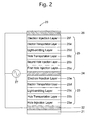
- FIG. 1 illustrates one example of the organic EL light-emitting device of the present invention in which the layer position number (n) is 8.
- the organic EL light-emitting device 1 has a substrate 10, and electrode layers and the organic EL light-emitting structures are alternately laminated on the substrate 10 in the following order: first electrode layer 11a, first organic EL light-emitting structure 11b, second electrode layer 12a, second organic EL light-emitting structure 12b, third electrode layer 13a, third organic EL light-emitting structure 13b, fourth electrode layer 14a, fourth organic EL light-emitting structure 14b, fifth electrode layer 15a, fifth organic EL light-emitting structure 15b, sixth electrode layer 16a, sixth organic EL light-emitting structure 16b, seventh electrode layer 17a, seventh organic EL light-emitting structure 17b, and eighth electrode layer 18a.
- a group of the electrode layers formed in an odd-numbered layer position from the substrate 10, that is, first electrode layer 11a, third electrode layer 13a, fifth electrode layer 15a and seventh electrode layer 17a are connected to an alternating electric source 19 as shown with the solid line in Figure 1 so that the electrode layers are electrically connected to each other to be in a same potential.
- a group of the electrode layers formed in an even-numbered layer position from the substrate 10, that is, second electrode layer 12a, fourth electrode layer 14a, sixth electrode layer 16a and eighth electrode layer 18a are connected to an alternating electric source 19 as shown with the broken line in Figure 1 so that the electrode layers are electrically connected to each other to be in a same potential.
- the organic EL light-emitting structures 11b, 12b, 13b, 14b, 15b, 16b and 17b each is disposed in the EL device 1 in such a manner that hole are injected from a side of the substrate 10, and electrons are injected from the side which is far from the substrate 10 (biasing direction in each organic EL light-emitting structure is identical to each other). Accordingly, light is emitted from the EL light-emitting structures 11b to 17b under the conditions that in the two electrode layers sandwiching the light-emitting structure, a positive (+) voltage is applied to the electrode layer on the side of the substrate 10 and a negative (-) voltage is applied to the electrode layer on the side far from the substrate 10. No light is emitted in the structure when the negative (-) voltage is applied to the electrode layer on the side of the substrate 10 and positive (+) voltage is applied to the electrode layer on the side far from the substrate 10.
- this organic EL device 1 when all of the electrode layers 11a to 18a are constituted from a transparent electrode and the substrate 10 is transparent as in the glass substrate, since the organic EL light-emitting structures 11b to 17b are also transparent, it becomes possible to obtain light emission in both the side of the substrate 10 or the side of the eighth electrode layer 18a in the EL device 1.
- the first electrode layer 11a and the eighth electrode layer 18a is constituted from an opaque electrode (including a light reflection layer consisting of metal) and the second electrode layer 12a to the seventh electrode layer 17a each is constituted from a transparent electrode, light generated in the organic EL light-emitting structures 11b to 17b can be emitted from either one of the side of the substrate 10 and the side of the eighth electrode layer 18a in the EL device 1.
- the opaque electrode may be any one of the first electrode layer 11a to the eighth electrode layer 18a.
- the organic EL light-emitting structures 11b to 17b may have the typical structures disclosed in, for example, the above-described Kodak patents and other literatures, that is, the structure containing only one organic EL light-emitting unit in which the layer structure is typically "anode/hole-transporting layer/light-emitting layer/electron-transporting layer/cathode", or they may have the so-called MPE (multi-photon emission) type organic EL device structure suggested by the present applicant and described above, that is, a combination of two or more organic EL light-emitting units in which the organic EL light-emitting units (each light-emitting unit comprises typically the layer structure section "hole-transporting layer/light-emitting layer/electron-transporting layer") are laminated in sequence through the insulating (i.e. in floating state) charge generation layer (CGL) so that light is simultaneously emitted in the light-emitting units.
- MPE multi-photon emission type organic EL device
- the alternating current-driving type organic EL device according to the present invention can be advantageously used as an illumination light source or in a display device.
- the commercial electric source used therein is an alternating electric source, it is appreciated that the EL device of the present invention is inevitably preferable to the prior art EL devices because of its structure capable of being driven without using an inverter.
- the frequency applied to the EL devices is suitably modified depending upon the use of the EL devices.
- the formation of the organic compound, metal oxide, metal and ITO transparent electrode as a film or layer was carried out by using a vacuum deposition apparatus commercially available from Vieetech Japan Co., Ltd. or the sputtering apparatus commercially available from FTS Corporation. Further, the control in the deposition rate of the vapor deposition materials and in the thickness of the deposited layers was carried out by using a thickness monitor with a quartz oscillator, "CRTM-8000" of ULVAC Co., attached to the vapor deposition apparatus. Furthermore, to determine an actual layer thickness after the layer formation, a stylus step meter, "P10" of Tencor Co. was used. The characteristics of the devices were evaluated with the source meter "2400" of KEITHLEY Co.
- the alternating voltage applied to the EL devices was controlled using a sliding voltage controller (slidac) operated at 50Hz.
- a light emission spectrum of the EL devices was measured using the optical multi-channel analyzer "PMA-11" of Hamamatsu Photonics Co. with the driving at the constant electric current.
- the alternating current-driving organic EL device of this example has the structure illustrated in Figure 2.
- the organic EL device 20 comprises a glass substrate 21 and a third electrode layer 26 between which a first electrode layer 22, a first organic EL light-emitting structure 23, a second electrode layer 24 and a second organic EL light-emitting structure 25 are laminated in this order on the substrate 21.
- a glass substrate having a size of 3cm x 3cm is prepared.
- the glass substrate 21 has coated thereon, as a first electrode layer 22, a 2mm width pattern of the ITO (indium-tin oxide; Nippon Sheet Glass Co., Ltd.) having a sheet resistance of about 10 ⁇ /sq.
- the substrate 21 is carefully washed with pure water and isopropyl alcohol (IPA), in sequence, followed by dry washing in an UV ozone apparatus ("UV-300", product of SAMCO International Co.).
- an organic coating for the formation of the first organic EL light-emitting structure 23 shown in Figure 2 is formed using an area-controlling mask 31 for the formation of the organic EL light-emitting structure shown in Figure 4A.
- the area-controlling mask 31 for the formation of the organic EL light-emitting structure has a rectangular opening section 31a in a central portion thereof, and the peripheral portion surrounding the opening section 31a constitutes a shielding or masking section 31b.
- the layers of the first organic EL light-emitting structure 23 are formed in accordance with the following method. First, onto the first electrode layer 22, a layer of an arylamine compound, "HI-406" (unknown molecular structure) commercially available from Idemitsu Kosan Co., Ltd. as a hole injection layer 23a, about 800 ⁇ thick, was deposited.
- HI-406 unknown molecular structure
- Alq an aluminum complex of tris(8-quinolinolato) represented by the following formula: as an electron transporting layer 23d, about 100 ⁇ thick.
- Alq an aluminum complex of tris(8-quinolinolato)
- an electron injection layer 23e i.e., "(in-situ) thermal reducing reaction generating layer” which was disclosed by the present applicant and others in Japanese Unexamined Patent Publication (Kokai) No. 2000-182774 (US Patent No. 6,396,209; European Patent No.
- the aluminum complex "Alq” described above and (8-quinolinato) lithium complex (hereinafter, referred to as "Liq") represented by the following formula: are co-deposited at a molar ratio of 1:1 onto the electron transporting layer 23d.
- the electron injection layer 23e about 50 ⁇ thick, is thus obtained.
- a layer of aluminum as a thermal reducing metal at an amount corresponding to the thickness of about 15 ⁇ to form an "in-situ" thermal reducing reaction generating layer (not shown in the Fig.) was deposited.
- the first organic EL light-emitting structure 23 is thus formed.
- the structure of the resulting first organic EL light-emitting structure 23 can be simply denoted as follows: HI-406/HT-320/RD-001X:BH-140/Alq/Alq:Liq+Al.
- the area-controlling mask 32 for the formation of the second electrode layer has two and parallel long-rectangular opening sections 32a, each of which is extended from the two opposed sides of the mask 32 to end at a central portion thereof.
- the mask area not constituting the opening sections 32a constitutes a shielding or masking section 32b. Note in the production of the EL devices having 4 or more electrode layers that the area-controlling mask 32 for the formation of the second electrode layer described above is used in the formation of the electrodes in an even-numbered layer position from the substrate.
- an organic material film for the formation of the second organic EL light-emitting structure 25 shown in Figure 2 is formed using an area-controlling mask 31 for the formation of the organic EL light-emitting structure shown in Figure 4A.
- the layers of the second organic EL light-emitting structure 25 are formed in accordance with the following method.
- a first hole injection layer 25a is formed in the method disclosed by the present applicant and others in Japanese Patent Application No. 2003-358402. That is, a mixed layer of HI-406 and vanadium pentoxide (V 2 O 5 ) is co-deposited at a molar ratio of 1:1 to form the first hole injection layer 25a having a thickness of about 100 ⁇ (Angstrom).
- the first hole injection layer 25a is introduced in this second organic EL light-emitting structure 25 for the purpose of enabling hole injection from the IZO constituting the second electrode layer 24 to be easy without causing energy barrier (i.e. enabling ohmic contact between the layers).
- a layer of HI-406 as a second hole injection layer 25b, 1,400 ⁇ thick was deposited onto the first hole injection layer 25a.
- a layer of HT-320 as a hole transporting layer 25c, 200 ⁇ thick was deposited onto the second hole injection layer 25b.
- a light-emitting layer 25d about 400 ⁇ thick, was deposited (i.e. co-deposition of "BD-102" and "BH-140" in the ratio of 4wt% of "BD-102").
- Alq is deposited to form an electron transportation layer 25e having a thickness of about 100 ⁇
- Alq and Liq are co-deposited to form a co-deposition layer of Alq:Liq having a thickness of about 50 ⁇ as an electron injection layer 25f.
- the second organic EL light-emitting structure 25 onto the co-deposition layer of Alq:Liq, a layer of aluminum acting as both of a thermal reducing metal and a material for forming a "third electrode layer", 1,000 ⁇ thick, was deposited in the presence of an area-controlling mask 33 for the formation of the third electrode layer (area-controlling mask for the formation of the odd-numbered electrode layers) shown in Figure 4C to simultaneously form a "in-situ" thermal reducing reaction generating layer (not shown in Figures) and the third electrode layer 26.
- the area-controlling mask 33 for the formation of the third electrode layer has two pairs of two and parallel long-rectangular opening sections 33a in a central portion thereof.
- the mask area not constituting the opening sections 33a constitutes a shielding or masking section 33b. Note in the production of the EL devices having 4 or more electrode layers that the area-controlling mask 33 for the formation of the third electrode layer described above is used in the formation of the electrodes in an odd-numbered layer position from the substrate.
- the organic EL device having the structure illustrated in Figure 2 and being simply denoted as follows is thus completed: "ITO/HI-406/HT-320/RD-001X:BH-140/Alq/Alq:Liq+Al/IZO/V 2 O 5 :HI-406/HI-406/HT-320/BD-102:BH-140/Alq/Alq:Liq/Al". Note in this structure that the section "V 2 O 5 :HI-406/HI-406/HT-320/BD-102:BH-140/Alq/Alq:Liq" corresponds to a second organic EL light-emitting structure 25.
- the third electrode layer 26 and the first electrode layer 22 are formed in the substantially same area when seen from an upper position of the glass substrate 21, and their ends are contacted with each other.
- these odd-numbered electrode layers are in a same potential.
- light is emitted in each of the section 29 sandwiched by the first electrode layer 22 and the second electrode layer 24 and the section 29 sandwiched by the second electrode layer 24 and the third electrode layer 26.
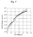
- a DC voltage or AC voltage was applied to the organic EL device 20 produced in Example 1, described above, under the below-mentioned measurement conditions to obtain the following results.
- the first electrode layer 22 and the third electrode layer 26 which are in a same potential to each other as described above were biased to an anode (+) and the second electrode layer 24 was biased to a cathode (-) to apply a DC voltage to the device 20, thereby generating light emission in only the first organic EL light-emitting structure 23. Under this condition, no light was emitted in the second organic EL light-emitting structure 25 because of reverse biasing to this structure.
- the light emission characteristics of the first organic EL light-emitting structure 23 are plotted with the white circle plots (o) in Figs. 7 and 8. Further, the light emission spectrum in the first organic EL light-emitting structure 23 (at the DC current density of 10 mA/cm 2 at the voltage of 8.0V) is plotted with the dashed line in Figure 10. Furthermore, the light emission appearance of the first organic EL light-emitting structure 23 is shown in Figs. 11 (photograph) and 12 (see, the light emissive section 43).
- the first electrode layer 22 and the third electrode layer 26 were biased to a cathode (-)and the second electrode layer 24 was biased to an anode (+) to apply a DC voltage to the device 20, thereby generating light emission in only the second organic EL light-emitting structure 25.
- no light was emitted in the first organic EL light-emitting structure 23 because of reverse biasing to this structure.
- the light emission characteristics of the second organic EL light-emitting structure 25 are plotted with the black circle plots (•) in Figs. 7 and 8.
- the light emission spectrum in the second organic EL light-emitting structure 25 (at the DC current density of 10 mA/cm 2 at the voltage of 8.3V) is plotted with the broken line in Figure 10. Furthermore, the light emission appearance of the second organic EL light-emitting structure 25 are shown in Figs. 11 and 12 (see, the light emissive section 45).
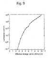
- the measurements were carried out by driving the organic EL device 20 produced in Example 1 under the alternating current conditions, thereby generating alternate light emission in the first organic EL light-emitting structure 23 and the second organic EL light-emitting structure 25.
- an AC voltage of 50Hz was applied from the AC electric source 27 between the first electrode layer 22 as well as the third electrode layer 26 which have the same potential to each other and the second electrode layer 24 to determine a luminance per the applied effective voltage.
- the light emission spectrum, obtained upon application of the AC effective voltage of 10V, in the AC-driven organic EL device is plotted with the solid line in Figure 10.
- the elapsed time required to measure the light emission spectrum was set to be about 0.2 seconds.
- the light emission appearance of the EL device are shown in Figs. 11 and 12 (see, the light emissive section 47).
- the organic EL device 20 can emit light continuously and thus without interruption, even if the device is driven with an alternating voltage.
- the organic EL light-emitting structures having different emission light colors were used by intention.
- the organic electroluminescent device comprises at least three groups of the electrode layers, and light can be alternately emitted in two or more organic electroluminescent light-emitting structures sandwiched between two groups of the electrode layers, it becomes possible to obtain organic electroluminescent device having no flickering problem observed in the prior art organic electroluminescent devices, and exhibiting an improved durability.
Applications Claiming Priority (2)
| Application Number | Priority Date | Filing Date | Title |
|---|---|---|---|
| JP2004055792A JP4276109B2 (ja) | 2004-03-01 | 2004-03-01 | 有機エレクトロルミネッセント素子 |
| JP2004055792 | 2004-03-01 |
Publications (2)
| Publication Number | Publication Date |
|---|---|
| EP1571709A2 true EP1571709A2 (fr) | 2005-09-07 |
| EP1571709A3 EP1571709A3 (fr) | 2006-11-02 |
Family
ID=34747595
Family Applications (1)
| Application Number | Title | Priority Date | Filing Date |
|---|---|---|---|
| EP05003783A Withdrawn EP1571709A3 (fr) | 2004-03-01 | 2005-02-22 | Dispositifs électroluminescents organiques |
Country Status (6)
| Country | Link |
|---|---|
| US (1) | US20050189875A1 (fr) |
| EP (1) | EP1571709A3 (fr) |
| JP (1) | JP4276109B2 (fr) |
| KR (1) | KR20060042177A (fr) |
| CN (1) | CN1665360A (fr) |
| TW (1) | TW200531586A (fr) |
Cited By (9)
| Publication number | Priority date | Publication date | Assignee | Title |
|---|---|---|---|---|
| EP1808909A1 (fr) * | 2006-01-11 | 2007-07-18 | Novaled AG | Dispositif électroluminescent |
| WO2007083918A1 (fr) | 2006-01-18 | 2007-07-26 | Lg Chem. Ltd. | Delo possédant des unités électroluminescentes organiques empilées |
| GB2443314A (en) * | 2006-10-24 | 2008-04-30 | Fuji Electric Holdings Co | A method of maufacturing a white light emitting organic EL device |
| DE102008025755A1 (de) * | 2008-05-29 | 2009-12-03 | Osram Opto Semiconductors Gmbh | Organisches Licht emittierendes Bauteil und Leuchtmittel mit einem solchen Bauteil |
| WO2010001769A1 (fr) * | 2008-06-30 | 2010-01-07 | Canon Kabushiki Kaisha | Appareil électroluminescent |
| US7763882B2 (en) | 1999-12-31 | 2010-07-27 | Lg Chem, Ltd. | Organic light-emitting device comprising buffer layer and method for fabricating the same |
| US8253126B2 (en) | 1999-12-31 | 2012-08-28 | Lg Chem. Ltd. | Organic electronic device |
| US8680562B2 (en) | 2005-03-22 | 2014-03-25 | Semiconductor Energy Laboratory Co., Ltd. | Light emitting device |
| WO2015003999A1 (fr) * | 2013-07-09 | 2015-01-15 | Osram Oled Gmbh | Agencement de composants optoélectroniques, procédé de fabrication d'un agencement de composants optoélectroniques, procédé permettant de faire fonctionner un agencement de composants optoélectroniques |
Families Citing this family (36)
| Publication number | Priority date | Publication date | Assignee | Title |
|---|---|---|---|---|
| WO2006015567A1 (fr) | 2004-08-13 | 2006-02-16 | Novaled Ag | Ensemble de couches pour un composant émetteur de lumière |
| DE502005002342D1 (de) * | 2005-03-15 | 2008-02-07 | Novaled Ag | Lichtemittierendes Bauelement |
| US7755275B2 (en) * | 2005-03-28 | 2010-07-13 | Panasonic Corporation | Cascaded light emitting devices based on mixed conductor electroluminescence |
| DE502005002218D1 (de) | 2005-04-13 | 2008-01-24 | Novaled Ag | Anordnung für eine organische Leuchtdiode vom pin-Typ und Verfahren zum Herstellen |
| US7531959B2 (en) * | 2005-06-29 | 2009-05-12 | Eastman Kodak Company | White light tandem OLED display with filters |
| JP4692415B2 (ja) * | 2005-09-15 | 2011-06-01 | カシオ計算機株式会社 | エレクトロルミネッセンス素子の製造方法 |
| DE502005004675D1 (de) * | 2005-12-21 | 2008-08-21 | Novaled Ag | Organisches Bauelement |
| EP1804309B1 (fr) * | 2005-12-23 | 2008-07-23 | Novaled AG | Dispositif électronique avec une structure en couches de nature organique |
| EP1848049B1 (fr) * | 2006-04-19 | 2009-12-09 | Novaled AG | Dispositif d'émission de lumière |
| KR100825384B1 (ko) * | 2006-05-16 | 2008-04-29 | 삼성에스디아이 주식회사 | 백색 유기 전계 발광 표시 장치 및 그 제조 방법 |
| DE102007019260B4 (de) * | 2007-04-17 | 2020-01-16 | Novaled Gmbh | Nichtflüchtiges organisches Speicherelement |
| KR100879476B1 (ko) * | 2007-09-28 | 2009-01-20 | 삼성모바일디스플레이주식회사 | 유기 발광 소자 |
| KR101420427B1 (ko) * | 2007-10-09 | 2014-07-16 | 엘지디스플레이 주식회사 | 유기전계 발광소자 |
| KR20090050369A (ko) | 2007-11-15 | 2009-05-20 | 삼성모바일디스플레이주식회사 | 유기 발광 소자 |
| KR100918401B1 (ko) | 2007-12-24 | 2009-09-24 | 삼성모바일디스플레이주식회사 | 유기 발광 소자 |
| KR100894066B1 (ko) | 2007-12-28 | 2009-04-24 | 삼성모바일디스플레이 주식회사 | 유기 발광 소자 |
| KR100898075B1 (ko) | 2008-03-04 | 2009-05-18 | 삼성모바일디스플레이주식회사 | 유기 발광 소자 |
| DE102008036063B4 (de) * | 2008-08-04 | 2017-08-31 | Novaled Gmbh | Organischer Feldeffekt-Transistor |
| DE102008036062B4 (de) | 2008-08-04 | 2015-11-12 | Novaled Ag | Organischer Feldeffekt-Transistor |
| US20110248244A1 (en) * | 2009-10-05 | 2011-10-13 | Emagin Corporation | Independently controlled stacked inverted organic light emitting diodes and a method of manufacturing same |
| JP2012003925A (ja) | 2010-06-16 | 2012-01-05 | Sony Corp | 表示装置 |
| US8994011B2 (en) | 2010-08-17 | 2015-03-31 | Lg Chem, Ltd. | Organic light-emitting device |
| DE102012102910B4 (de) * | 2012-04-03 | 2016-09-22 | Novaled Ag | Vertikaler organischer Transistor und Verfahren zum Herstellen |
| KR101539842B1 (ko) * | 2012-05-31 | 2015-07-28 | 주식회사 엘지화학 | 유기 발광 소자 |
| KR102040872B1 (ko) * | 2012-12-13 | 2019-11-06 | 삼성디스플레이 주식회사 | 유기발광소자, 이를 포함하는 유기발광표시장치, 및 유기발광소자를 양면 발광 제어하는 방법 |
| DE102012112796B4 (de) * | 2012-12-20 | 2019-09-19 | Novaled Gmbh | Vertikaler organischer Transistor, Schaltungsanordnung und Anordnung mit vertikalem organischen Transistor sowie Verfahren zum Herstellen |
| CN104078568A (zh) * | 2013-03-29 | 2014-10-01 | 海洋王照明科技股份有限公司 | 有机电致发光器件及其制备方法 |
| WO2016132460A1 (fr) * | 2015-02-17 | 2016-08-25 | パイオニア株式会社 | Dispositif électroluminescent |
| KR102388253B1 (ko) * | 2015-11-06 | 2022-04-20 | 삼성디스플레이 주식회사 | 유기 발광 소자 |
| CN107104128B (zh) * | 2017-05-11 | 2021-04-27 | 京东方科技集团股份有限公司 | 一种像素单元及驱动方法、显示面板、显示装置 |
| CN107170779A (zh) * | 2017-05-12 | 2017-09-15 | 京东方科技集团股份有限公司 | 一种oled显示基板及显示装置 |
| CN107863445A (zh) * | 2017-10-30 | 2018-03-30 | 武汉华美晨曦光电有限责任公司 | 一种以交流驱动的白光oled器件 |
| CN107958962A (zh) * | 2017-11-21 | 2018-04-24 | 合肥鑫晟光电科技有限公司 | Oled器件及其驱动方法、oled基板及其制作方法、显示装置 |
| CN109037467B (zh) * | 2018-08-13 | 2020-07-10 | 京东方科技集团股份有限公司 | 一种电致发光器件、显示面板及显示装置 |
| CN110611034A (zh) * | 2019-08-29 | 2019-12-24 | 深圳市华星光电半导体显示技术有限公司 | 一种有机电致发光器件和显示面板 |
| CN112909053A (zh) * | 2021-01-26 | 2021-06-04 | 京东方科技集团股份有限公司 | 显示装置、显示面板及其制造方法 |
Family Cites Families (25)
| Publication number | Priority date | Publication date | Assignee | Title |
|---|---|---|---|---|
| US4539507A (en) * | 1983-03-25 | 1985-09-03 | Eastman Kodak Company | Organic electroluminescent devices having improved power conversion efficiencies |
| US4885211A (en) * | 1987-02-11 | 1989-12-05 | Eastman Kodak Company | Electroluminescent device with improved cathode |
| US4769292A (en) * | 1987-03-02 | 1988-09-06 | Eastman Kodak Company | Electroluminescent device with modified thin film luminescent zone |
| US5552678A (en) * | 1994-09-23 | 1996-09-03 | Eastman Kodak Company | AC drive scheme for organic led |
| JP4477150B2 (ja) * | 1996-01-17 | 2010-06-09 | 三星モバイルディスプレイ株式會社 | 有機薄膜el素子 |
| JP3808534B2 (ja) * | 1996-02-09 | 2006-08-16 | Tdk株式会社 | 画像表示装置 |
| JPH10270171A (ja) * | 1997-01-27 | 1998-10-09 | Junji Kido | 有機エレクトロルミネッセント素子 |
| US6337492B1 (en) * | 1997-07-11 | 2002-01-08 | Emagin Corporation | Serially-connected organic light emitting diode stack having conductors sandwiching each light emitting layer |
| JPH11251067A (ja) * | 1998-03-02 | 1999-09-17 | Junji Kido | 有機エレクトロルミネッセント素子 |
| JPH11312584A (ja) * | 1998-04-28 | 1999-11-09 | Tdk Corp | 有機el素子 |
| JP4505067B2 (ja) * | 1998-12-16 | 2010-07-14 | 淳二 城戸 | 有機エレクトロルミネッセント素子 |
| US6268695B1 (en) * | 1998-12-16 | 2001-07-31 | Battelle Memorial Institute | Environmental barrier material for organic light emitting device and method of making |
| KR20010050711A (ko) * | 1999-09-29 | 2001-06-15 | 준지 키도 | 유기전계발광소자, 유기전계발광소자그룹 및 이런소자들의 발광스펙트럼의 제어방법 |
| JP2001203077A (ja) * | 2000-01-18 | 2001-07-27 | Tohoku Pioneer Corp | 有機el素子の駆動方法及び駆動装置 |
| JP3983037B2 (ja) * | 2001-11-22 | 2007-09-26 | 株式会社半導体エネルギー研究所 | 発光装置およびその作製方法 |
| JP3933591B2 (ja) * | 2002-03-26 | 2007-06-20 | 淳二 城戸 | 有機エレクトロルミネッセント素子 |
| JP2003303683A (ja) * | 2002-04-09 | 2003-10-24 | Semiconductor Energy Lab Co Ltd | 発光装置 |
| JP2004031214A (ja) * | 2002-06-27 | 2004-01-29 | Matsushita Electric Ind Co Ltd | 有機電界発光素子 |
| US7034470B2 (en) * | 2002-08-07 | 2006-04-25 | Eastman Kodak Company | Serially connecting OLED devices for area illumination |
| US6936964B2 (en) * | 2002-09-30 | 2005-08-30 | Eastman Kodak Company | OLED lamp |
| JP2004170487A (ja) * | 2002-11-18 | 2004-06-17 | Rohm Co Ltd | 有機elディスプレイ素子及び有機elディスプレイ素子の駆動方法 |
| US6991859B2 (en) * | 2003-03-18 | 2006-01-31 | Eastman Kodak Company | Cascaded organic electroluminescent devices |
| JP3755521B2 (ja) * | 2003-06-13 | 2006-03-15 | セイコーエプソン株式会社 | 有機el装置とその駆動方法、照明装置、及び電子機器 |
| WO2005015640A1 (fr) * | 2003-08-12 | 2005-02-17 | Philips Intellectual Property & Standards Gmbh | Agencement de circuits de commande a courant alternatif de diodes organiques |
| JP2005174639A (ja) * | 2003-12-09 | 2005-06-30 | Seiko Epson Corp | 有機el装置、および電子機器 |
-
2004
- 2004-03-01 JP JP2004055792A patent/JP4276109B2/ja not_active Expired - Lifetime
-
2005
- 2005-02-22 TW TW094105217A patent/TW200531586A/zh unknown
- 2005-02-22 EP EP05003783A patent/EP1571709A3/fr not_active Withdrawn
- 2005-02-23 CN CN200510008598XA patent/CN1665360A/zh active Pending
- 2005-02-24 KR KR1020050015577A patent/KR20060042177A/ko not_active IP Right Cessation
- 2005-02-25 US US11/065,937 patent/US20050189875A1/en not_active Abandoned
Non-Patent Citations (1)
| Title |
|---|
| None * |
Cited By (17)
| Publication number | Priority date | Publication date | Assignee | Title |
|---|---|---|---|---|
| US8253126B2 (en) | 1999-12-31 | 2012-08-28 | Lg Chem. Ltd. | Organic electronic device |
| US7763882B2 (en) | 1999-12-31 | 2010-07-27 | Lg Chem, Ltd. | Organic light-emitting device comprising buffer layer and method for fabricating the same |
| US8890204B2 (en) | 2005-03-22 | 2014-11-18 | Semiconductor Energy Laboratory Co., Ltd. | Light emitting device |
| US8680562B2 (en) | 2005-03-22 | 2014-03-25 | Semiconductor Energy Laboratory Co., Ltd. | Light emitting device |
| WO2007082674A2 (fr) * | 2006-01-11 | 2007-07-26 | Novaled Ag | Dispositif d'émission de lumière électroluminescent comprenant un ensemble de couches organiques et procédé de production de ce dispositif |
| WO2007082674A3 (fr) * | 2006-01-11 | 2008-01-24 | Novaled Ag | Dispositif d'émission de lumière électroluminescent comprenant un ensemble de couches organiques et procédé de production de ce dispositif |
| EP1808909A1 (fr) * | 2006-01-11 | 2007-07-18 | Novaled AG | Dispositif électroluminescent |
| WO2007083918A1 (fr) | 2006-01-18 | 2007-07-26 | Lg Chem. Ltd. | Delo possédant des unités électroluminescentes organiques empilées |
| EP1974590A1 (fr) * | 2006-01-18 | 2008-10-01 | LG Chemical Limited | Delo possédant des unités électroluminescentes organiques empilées |
| EP1974590A4 (fr) * | 2006-01-18 | 2009-11-11 | Lg Chemical Ltd | Delo possédant des unités électroluminescentes organiques empilées |
| CN101371619B (zh) * | 2006-01-18 | 2013-11-13 | Lg化学株式会社 | 具有堆叠式有机发光单元的oled |
| GB2443314A (en) * | 2006-10-24 | 2008-04-30 | Fuji Electric Holdings Co | A method of maufacturing a white light emitting organic EL device |
| GB2443314B (en) * | 2006-10-24 | 2011-03-16 | Fuji Electric Holdings Company Ltd | Method of manufacturing a white light emitting organic EL device |
| US8686440B2 (en) | 2008-05-29 | 2014-04-01 | Osram Opto Semiconductors Gmbh | Organic light emitting component and illumination means comprising a component of this type |
| DE102008025755A1 (de) * | 2008-05-29 | 2009-12-03 | Osram Opto Semiconductors Gmbh | Organisches Licht emittierendes Bauteil und Leuchtmittel mit einem solchen Bauteil |
| WO2010001769A1 (fr) * | 2008-06-30 | 2010-01-07 | Canon Kabushiki Kaisha | Appareil électroluminescent |
| WO2015003999A1 (fr) * | 2013-07-09 | 2015-01-15 | Osram Oled Gmbh | Agencement de composants optoélectroniques, procédé de fabrication d'un agencement de composants optoélectroniques, procédé permettant de faire fonctionner un agencement de composants optoélectroniques |
Also Published As
| Publication number | Publication date |
|---|---|
| EP1571709A3 (fr) | 2006-11-02 |
| US20050189875A1 (en) | 2005-09-01 |
| JP2005251398A (ja) | 2005-09-15 |
| CN1665360A (zh) | 2005-09-07 |
| JP4276109B2 (ja) | 2009-06-10 |
| TW200531586A (en) | 2005-09-16 |
| KR20060042177A (ko) | 2006-05-12 |
Similar Documents
| Publication | Publication Date | Title |
|---|---|---|
| EP1571709A2 (fr) | Dispositifs électroluminescents organiques | |
| KR100835725B1 (ko) | 유기전계발광소자 | |
| KR100858111B1 (ko) | 유기전계발광소자 | |
| KR100880878B1 (ko) | 유기소자, 유기전계발광소자, 유기태양전지,유기fet구조, 및 유기소자의 제조방법 | |
| KR101290610B1 (ko) | 유기 전계 발광 소자 및 그 제조 방법 | |
| KR100894306B1 (ko) | 유기전계발광소자 | |
| KR100880881B1 (ko) | 유기소자들, 유기전계발광소자들 및 유기태양전지들 | |
| TWI485899B (zh) | 有機電致發光元件 | |
| JP4961412B2 (ja) | 有機素子、及び、有機素子の製造方法 | |
| JP5452853B2 (ja) | 有機エレクトロルミネッセンス素子 | |
| JP4966176B2 (ja) | 有機エレクトロルミネッセンス素子 | |
| KR20080090988A (ko) | 유기 일렉트로루미네선스 소자 | |
| WO2011010696A1 (fr) | Élément électroluminescent organique | |
| JPH11149985A (ja) | 無機電子輸送層を有する有機エレクトロルミネセンスデバイス | |
| US20080003455A1 (en) | Organic El Device | |
| KR101190108B1 (ko) | 유기 전계발광 소자 및 그 제조 방법 | |
| US7170224B2 (en) | Electrode for organic light emitting device and organic light emitting device comprising the same | |
| JP2007123865A (ja) | 有機電界発光素子 | |
| JP4872805B2 (ja) | 有機エレクトロルミネッセンス素子 | |
| KR100547055B1 (ko) | 유기 전계발광 소자 | |
| JP2008053557A (ja) | 有機エレクトロルミネッセンス素子 | |
| JP5281271B2 (ja) | 有機エレクトロルミネッセンス素子 | |
| KR100581639B1 (ko) | 유기 전계발광 소자 | |
| JP2010033973A (ja) | 有機エレクトロルミネッセンス素子 | |
| KR20150037710A (ko) | 적층 유기 발광소자 |
Legal Events
| Date | Code | Title | Description |
|---|---|---|---|
| PUAI | Public reference made under article 153(3) epc to a published international application that has entered the european phase |
Free format text: ORIGINAL CODE: 0009012 |
|
| AK | Designated contracting states |
Kind code of ref document: A2 Designated state(s): AT BE BG CH CY CZ DE DK EE ES FI FR GB GR HU IE IS IT LI LT LU MC NL PL PT RO SE SI SK TR |
|
| AX | Request for extension of the european patent |
Extension state: AL BA HR LV MK YU |
|
| PUAL | Search report despatched |
Free format text: ORIGINAL CODE: 0009013 |
|
| AK | Designated contracting states |
Kind code of ref document: A3 Designated state(s): AT BE BG CH CY CZ DE DK EE ES FI FR GB GR HU IE IS IT LI LT LU MC NL PL PT RO SE SI SK TR |
|
| AX | Request for extension of the european patent |
Extension state: AL BA HR LV MK YU |
|
| 17P | Request for examination filed |
Effective date: 20061214 |
|
| 17Q | First examination report despatched |
Effective date: 20070208 |
|
| AKX | Designation fees paid |
Designated state(s): AT BE BG CH CY CZ DE DK EE ES FI FR GB GR HU IE IS IT LI LT LU MC NL PL PT RO SE SI SK TR |
|
| STAA | Information on the status of an ep patent application or granted ep patent |
Free format text: STATUS: THE APPLICATION IS DEEMED TO BE WITHDRAWN |
|
| 18D | Application deemed to be withdrawn |
Effective date: 20070821 |