EP1548845B1 - Procédé de traitement de particules de poudre - Google Patents
Procédé de traitement de particules de poudre Download PDFInfo
- Publication number
- EP1548845B1 EP1548845B1 EP03029577A EP03029577A EP1548845B1 EP 1548845 B1 EP1548845 B1 EP 1548845B1 EP 03029577 A EP03029577 A EP 03029577A EP 03029577 A EP03029577 A EP 03029577A EP 1548845 B1 EP1548845 B1 EP 1548845B1
- Authority
- EP
- European Patent Office
- Prior art keywords
- powder
- sulfur
- grains
- temperature
- powder particles
- Prior art date
- Legal status (The legal status is an assumption and is not a legal conclusion. Google has not performed a legal analysis and makes no representation as to the accuracy of the status listed.)
- Expired - Lifetime
Links
Images


Classifications
-
- C—CHEMISTRY; METALLURGY
- C01—INORGANIC CHEMISTRY
- C01B—NON-METALLIC ELEMENTS; COMPOUNDS THEREOF; METALLOIDS OR COMPOUNDS THEREOF NOT COVERED BY SUBCLASS C01C
- C01B19/00—Selenium; Tellurium; Compounds thereof
-
- H—ELECTRICITY
- H10—SEMICONDUCTOR DEVICES; ELECTRIC SOLID-STATE DEVICES NOT OTHERWISE PROVIDED FOR
- H10F—INORGANIC SEMICONDUCTOR DEVICES SENSITIVE TO INFRARED RADIATION, LIGHT, ELECTROMAGNETIC RADIATION OF SHORTER WAVELENGTH OR CORPUSCULAR RADIATION
- H10F77/00—Constructional details of devices covered by this subclass
- H10F77/10—Semiconductor bodies
- H10F77/12—Active materials
- H10F77/126—Active materials comprising only Group I-III-VI chalcopyrite materials, e.g. CuInSe2, CuGaSe2 or CuInGaSe2 [CIGS]
-
- H—ELECTRICITY
- H10—SEMICONDUCTOR DEVICES; ELECTRIC SOLID-STATE DEVICES NOT OTHERWISE PROVIDED FOR
- H10F—INORGANIC SEMICONDUCTOR DEVICES SENSITIVE TO INFRARED RADIATION, LIGHT, ELECTROMAGNETIC RADIATION OF SHORTER WAVELENGTH OR CORPUSCULAR RADIATION
- H10F10/00—Individual photovoltaic cells, e.g. solar cells
-
- H—ELECTRICITY
- H10—SEMICONDUCTOR DEVICES; ELECTRIC SOLID-STATE DEVICES NOT OTHERWISE PROVIDED FOR
- H10F—INORGANIC SEMICONDUCTOR DEVICES SENSITIVE TO INFRARED RADIATION, LIGHT, ELECTROMAGNETIC RADIATION OF SHORTER WAVELENGTH OR CORPUSCULAR RADIATION
- H10F71/00—Manufacture or treatment of devices covered by this subclass
-
- Y—GENERAL TAGGING OF NEW TECHNOLOGICAL DEVELOPMENTS; GENERAL TAGGING OF CROSS-SECTIONAL TECHNOLOGIES SPANNING OVER SEVERAL SECTIONS OF THE IPC; TECHNICAL SUBJECTS COVERED BY FORMER USPC CROSS-REFERENCE ART COLLECTIONS [XRACs] AND DIGESTS
- Y02—TECHNOLOGIES OR APPLICATIONS FOR MITIGATION OR ADAPTATION AGAINST CLIMATE CHANGE
- Y02E—REDUCTION OF GREENHOUSE GAS [GHG] EMISSIONS, RELATED TO ENERGY GENERATION, TRANSMISSION OR DISTRIBUTION
- Y02E10/00—Energy generation through renewable energy sources
- Y02E10/50—Photovoltaic [PV] energy
- Y02E10/541—CuInSe2 material PV cells
-
- Y—GENERAL TAGGING OF NEW TECHNOLOGICAL DEVELOPMENTS; GENERAL TAGGING OF CROSS-SECTIONAL TECHNOLOGIES SPANNING OVER SEVERAL SECTIONS OF THE IPC; TECHNICAL SUBJECTS COVERED BY FORMER USPC CROSS-REFERENCE ART COLLECTIONS [XRACs] AND DIGESTS
- Y02—TECHNOLOGIES OR APPLICATIONS FOR MITIGATION OR ADAPTATION AGAINST CLIMATE CHANGE
- Y02P—CLIMATE CHANGE MITIGATION TECHNOLOGIES IN THE PRODUCTION OR PROCESSING OF GOODS
- Y02P70/00—Climate change mitigation technologies in the production process for final industrial or consumer products
- Y02P70/50—Manufacturing or production processes characterised by the final manufactured product
Definitions
- the invention relates to a method for the treatment of powder grains.
- the method is particularly suitable for the treatment of powder grains, which consist of a Cu (In, Ga) Se 2 compound.
- the invention has for its object to provide a method by which the properties of a Cu (In, Ga) Se 2 powder can be improved in terms of use of this powder in a solar cell.
- a further object of the invention is to provide a monocorn membrane solar cell which has the highest possible efficiency.
- this object is achieved according to the invention by a method for the treatment of consisting of a Cu (In, Ga) Se 2 compound powder grains in which the powder grains and sulfur are added into a vessel and from the powder grains and the Sulfur content of the vessel is heated and kept at a constant temperature after heating.
- a foreign phase consisting of Cu, Ga or In can come from a phase of stoichiometric Cu (In, Ga) Se 2 , the foreign phases preferably being deposited on the surface of the powder grains.
- the powder grains are filled in a two-zone ampoule, wherein the powder grains are introduced into one of the zones and the sulfur into the other zone.
- the powder grains are then preferably heated to a temperature between 400 ° C and 600 ° C.
- the sulfur is preferably heated to a temperature of about 100 ° C.
- Powder grains and sulfur are held at the respective temperature for a period between one hour and 50 hours.
- a mixture consisting of powder grains and sulfur is filled into an ampoule.
- the mixture is then heated to a temperature between 300 ° C and 600 ° C and held at a temperature of between 5 minutes and 4 hours.
- a particularly advantageous temperature range is between 380 ° C and 410 ° C.
- an advantageous monocorn membrane solar cell is also provided, which is characterized by a particularly high efficiency compared to other monocorn membrane solar cells.
- the solar cell includes a back contact, a monocrome membrane, at least one semiconductor layer and a front contact and is characterized in that the Monokornmembran containing the invention treated powder grains.
- this solar cell Due to the advantageous properties of the grains treated according to the invention, this solar cell has a high degree of efficiency.
- the powder grains consisting of a Cu (In, Ga) Se 2 compound and the sulfur are filled in a so-called two-zone ampoule, wherein the powder grains in one zone and the sulfur in the other zone of the two Zone ampoule can be entered.
- a two-zone ampoule consists of a tube closed on both sides or closable, which has a taper in the middle.
- the shape of the ampoule resembles that of an egg timer.
- the two-zone ampoule is used horizontally in the process and should be made of a material that does not react with the filled substances. It therefore consists approximately of quartz glass.
- a typical filling quantity consists of 10 g powder grains and 2 g sulfur.
- the two-zone ampoule is evacuated and the sulfur in the one zone is heated to a temperature of about 100 ° C. As a result, gaseous S 2 is formed which spreads throughout the ampule.
- the powder grains in the other zone of the two-zone ampoule are heated to a temperature between 400 ° C and 600 ° C.
- the sulfur vapor pressure in the zone of the ampoule containing the powder grains can be varied by changing the temperature prevailing in this zone. It should be between 0.13 Pa and 133 Pa.
- Powder grains and sulfur are now kept at the respective temperature for a period between one hour and 50 hours. During this period, as explained at the outset, any foreign phases present on the surface of the powder grains and consisting of Cu, In and Ga are presumably converted into a Cu (In, Ga) S 2 compound.
- the ampoule is cooled and the sulfurized powder grains can be removed.
- a mixture consisting of the powder grains and the sulfur is filled into an ampoule which, for example, again consists of quartz glass.
- a typical mixture consists of 50 vol% powder and 50 vol% sulfur.
- the vial is evacuated and the mixture is heated to a temperature between 300 ° C and 600 ° C and preferably to a temperature between 380 ° C and 410 ° C.
- the sulfur is liquid and uniformly surrounds the powder grains which are in the solid phase at that temperature. The powder grains are so to speak "cooked" in the liquid sulfur.
- the period of time in which the mixture is maintained at the temperature reached after heating is between 5 minutes and 4 hours.
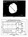
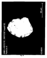
- Fig. 1a shows the optical micrograph of such a powder grain, which for 15 minutes at 410 ° C ("410 ° C, 15 '") and then for 30 minutes at 380 ° C ("380 ° C, 30'") in liquid S 2 was "cooked”.
- the figure also shows an analysis path ("analysis track").
- FIG. 1b The results of this study are shown in FIG. 1b by means of a graph.
- the horizontal axis indicates the distance from the edge of the powder grain at which an analysis is made and the vertical axis indicates the percentage by weight (wt.%) With which an element is present at the corresponding point of the powder grain.
- the chemical composition of the powder grain corresponds approximately to the composition of stoichiometric CuInSe 2 up to a distance of approximately 55 ⁇ m from the edge of the powder grain.
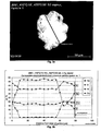
- FIGS. 2a to 4b show similar results for other powder grains.
- the figures can be taken in each case at what temperature and during which period the powder grains were treated. It is also stated whether the powder grains were "boiled” in liquid sulfur (liquid S2 ”) or whether the grains in the two-zone ampoule were treated with gaseous sulfur (" S2 vapor ").
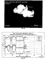
- FIG. 5b shows the result of a Se content of the powder grain analyzed in the electron micrograph of FIG. 5a, analyzed by the method of backscattered electron recording.
- the bright areas in FIG. 5b with a high density of white dots correspond to the areas with a high Se content, the dark areas correspond to sites with a low Se content.
- FIG. 5c shows the result of a backscatter electron pickup sensitive to the S content of the powder grain shown in the photograph in FIG. 5a.
- the bright areas in FIG. 5c correspond to areas with a high S content, the dark areas correspond to locations with a low S content.
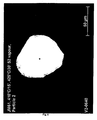
- FIGS. 6 to 10 show further light-microscopic photographs of polished powder grains.
- FIGS. 11 and 12 show the characteristics of solar cells in which the grains treated according to the invention were used as a function of various parameters of the treatment.
- the solar cells preferably consist of a back contact, a monograin membrane, at least one semiconductor layer and a front contact.
- the grains are first embedded in a preferably formed as a polymer membrane monocrystalline membrane, which was applied to the back contact of the solar cell.
- the back contact consists of an applied on a glass substrate electrically conductive adhesive.
- At least one further semiconductor layer is applied to the monocrystal membrane consisting of the grains embedded in the polymer membrane. It is preferably a CdS buffer layer and a layer consisting of intrinsic ZnO.
- FIG. 11 shows the no-load voltage V OC , the fill factor FF and the short-circuit current I of a solar cell containing the grains treated according to the invention as a function of the treatment temperature.
- the index P S indicates that the grains were subjected to sulfurization according to the invention.
- the results shown in FIG. 11 relate to sulfurization carried out in a two-zone ampoule at a specific, fixed temperature of sulfur.
- the power radiated into the solar cell was also set to a specific, fixed value during the measurement series. Filled rectangles, circles and non-filled rectangles indicate, as in FIG. 12, actual measuring points.
- FIG. 12 shows the dependence of the parameters on the other parameters of the treatment. The results also relate to the treatment in the two-zone ampoule and were taken up for powder grains, which was heated to a temperature of 530 ° C for the treatment.
- the grains were subjected to the treatment according to the invention with sulfur (P S ), and an analogous treatment in which sulfur was replaced by selenium (P Se ).
- the treatment with selenium was also carried out for powder grains which did not consist of a pure CuInSe 2 compound but contained an admixture of Ga (Ga + P Se ). According to the Interpretation of the success of sulfurization according to the invention is expected in the latter two treatment methods, a reaction of the foreign phases in Cu (In, Ga) Se 2 .
- the right side of the diagram in FIG. 12 shows the dependence of the parameters for sulfurization (annealing in S) on the duration of the treatment and the sulfur vapor pressure set in the zone containing the powder grains of the two-zone ampoule.
- the temperature in the zone containing the grains was 530 ° C and the sulfur vapor pressure was varied solely by a change in the prevailing in the sulfur-containing zone temperature.
- the measurement points refer to measurements on solar cells in the powder grains was used, which was a treatment 1 hour (1h), 5 minutes (5 '), 2 hours (2h) and 18 hours (18 hours) with a sulfur vapor pressure of 13.33 Pa (0.1 ton), 666.5 Pa (5 ton) and 1.33 Pa (0.01 ton).
- Cu and In and / or Cu and Ga are alloyed in this preferred method, wherein the amounts of moles of Cu used on the one hand and In and Ga on the other hand are dimensioned so that Cu-poor CuIn and CuGa alloys arise. It has been found to be particularly advantageous for the production of powder grains used in solar cells that the Cu / (In + Ga) ratio, ie the ratio of the molar amount of Cu used to the sum of the molar amount of In and the amount of mol used Ga, between 1 and 1: 1.2.
- the ratio of the molar amount of Ga used to the molar amount of In used is preferably between 0 and 0.43.
- a ratio of 0.43 corresponds approximately to a Ga content of 30%, based on the molar amount of In and Ga
- the process preferably produces those Cu (In, Ga) Se 2 compounds which, in their molar ratio between Ga and In, lie between this molar ratio of the compounds CuInSe 2 and CuGa 0.3 In 0.7 Se 2 .
- the alloys are then ground to a powder, where it has been found that the grain sizes of the produced Cu (In, Ga) Se 2 powder grains depend on the grain sizes of the powder produced from the CuIn and / or CuGa alloy. It is thus purposefully ground powder with a certain size of the grains contained.
- the powder consisting of the alloys CuIn and CuGa is now filled into an ampoule, which consists of a material that does not react with any of the substances to be added. It thus consists, for example, of quartz glass.
- Se is added in an amount corresponding to the stoichiometric proportion of this element to the Cu (In, Ga) Se 2 compound to be produced.
- the proportion of the flux on the subsequently formed melt typically being about 40% by volume.
- the amount of flux on the melt may be between 10 and 90% by volume.
- the ampoule is then evacuated and heated with the specified content to a temperature between 650 ° C and 810 ° C. During heating, Cu (In, Ga) Se 2 forms .
- the flux is melted at this temperature, so that the space between the grains is filled with a liquid phase, which serves as a transport medium.
- the melt is kept constant at the previously set temperature for a certain holding time. Depending on the desired grain size, a holding time between 5 minutes and 100 hours may be required. Typically, it is about 30 hours.
- Grain growth is interrupted by cooling the melt. It is very advantageous to quench the melt very quickly, for example within a few seconds.
- the flux is removed by triggering with water.
- the monocrystalline powder grains can then be removed from the ampoule.
- the suitable time course of temperature during heating and cooling as well as the holding time and the temperature to be maintained during the holding time are determined in preliminary tests.
- powders having an average diameter of the individual grains of 0.1 ⁇ m to 0.1 mm can be produced.
- the parameters A, n and E depend on the starting materials used, the flux and the specific growth processes not described here. If KI is used as a flux, then E is about 0.25 eV. The value of n in this case is between 3 and 4.
- mean grain size and the exact shape of the grain size distribution depend on the holding time, the temperature of the melt and the grain size of the powder consisting of the CuIn and CuGa alloys used. In addition, mean grain size and grain size distribution are influenced by the choice of flux.
- the grains which can be produced by the process are p-type and have a very good electrical conductivity.
- the electrical resistances of the prepared Cu (In, Ga) Se 2 powder grains were in a range of 100 ⁇ to 10 k ⁇ depending on the Cu / Ga ratio, Cu / (In + Ga) ratio and the temperature of the melt , This corresponds to a resistivity of 10 k ⁇ cm to 2 M ⁇ cm.
- the process allowed the production of monocrystalline powders whose grains had a very uniform composition.
- the powders are particularly suitable for the production of monocrystal membranes which are used in solar cells, it being possible to produce solar cells with a very high degree of efficiency using the powders prepared by the process and treated according to the process of the invention.
- the preparation process described here appears to have the particular advantage that, owing to the addition of a substoichiometric amount of Cu with respect to the compound to be produced, mainly Cu-poor powder grains are formed. This avoids the problem of phase segregation in the grains into stoichiometric CuInSe 2 and a metallic CuSe binary phase. Namely, this foreign phase preferentially accumulates on the surface of the grains and can cause short circuits in the solar cell.
- the described production process obviously has the advantage that the CuSe phase produced during the production of the grains remains in the flux and does not accumulate on the grains.
- the process thus makes it possible to produce a wide range of CuIn 1-x Ga x S y Se z compounds. These semiconductor compounds cover a range of bandgap energies between 1.04 eV and 2.5 eV.
- powder grains which have very good photovoltaic properties, which can be further improved by the sulfur treatment according to the invention.
- the powder grains are particularly suitable for use in a solar cell.
Landscapes
- Chemical & Material Sciences (AREA)
- Organic Chemistry (AREA)
- Inorganic Chemistry (AREA)
- Photovoltaic Devices (AREA)
- Glanulating (AREA)
- Cereal-Derived Products (AREA)
- Nonmetallic Welding Materials (AREA)
- Seeds, Soups, And Other Foods (AREA)
- Manufacture And Refinement Of Metals (AREA)
- Physical Or Chemical Processes And Apparatus (AREA)
Claims (9)
- Procédé pour le traitement de grains de poudre se composant d'un composé Cu(In,Ga)Se2,
caractérisé en ce que
les grains de poudre ainsi qu'une quantité de soufre sont introduits dans un récipient et en ce que le contenu du récipient se composant des grains et du soufre est chauffé et est maintenu à une température constante pendant une période de temps donnée. - Procédé selon la revendication 1,
caractérisé en ce que
les grains et le soufre sont versés dans une ampoule à deux zones, les grains étant introduits dans l'une des zones et la quantité de soufre dans l'autre zone. - Procédé selon l'une ou les deux revendications 1 et 2,
caractérisé en ce que
les grains sont chauffés à une température comprise entre 400 °C et 600 °C. - Procédé selon une ou plusieurs des revendications précédentes,
caractérisé en ce que
le soufre est chauffé à une température de l'ordre de 100 °C. - Procédé selon une ou plusieurs des revendications précédentes,
caractérisé en ce que
les grains et le soufre sont à chaque fois maintenus à température constante, pendant une période de temps comprise entre une heure et 50 heures. - Procédé selon la revendication 1,
caractérisé en ce que
un mélange se composant des grains de poudre et du soufre est versé dans une ampoule. - Procédé selon une ou les deux revendications 1 et 6,
caractérisé en ce que
le mélange se composant des grains de poudre et du soufre est chauffé et est maintenu à une température comprise entre 300 °C et 600 °C. - Procédé selon une ou plusieurs des revendications 1, 6 et 7
caractérisé en ce que
le mélange se composant de grains de poudre et de soufre est maintenu à une température donnée pendant une période de temps comprise entre 5 minutes et 4 heures. - Cellule solaire à membrane monogranulaire, comprenant un contact postérieur, une membrane monogranulaire, au moins une couche semi-conductrice et un contact frontal,
caractérisée en ce que
la membrane monogranulaire contient des grains de poudre traités avec un procédé selon une ou plusieurs des revendications 1 à 8.
Priority Applications (15)
| Application Number | Priority Date | Filing Date | Title |
|---|---|---|---|
| DE50305977T DE50305977D1 (de) | 2003-12-22 | 2003-12-22 | Verfahren zur Behandlung von Pulverkörner |
| PT03029577T PT1548845E (pt) | 2003-12-22 | 2003-12-22 | Processo para tratar partículas de pó |
| ES03029577T ES2279057T3 (es) | 2003-12-22 | 2003-12-22 | Procedimiento para tratar granos de polvo. |
| AT03029577T ATE348408T1 (de) | 2003-12-22 | 2003-12-22 | Verfahren zur behandlung von pulverkörner |
| SI200330667T SI1548845T1 (sl) | 2003-12-22 | 2003-12-22 | postopek za obdelavo prašnih zrn |
| DK03029577T DK1548845T3 (da) | 2003-12-22 | 2003-12-22 | Fremgangsmåde til behandling af pulverkorn |
| EP03029577A EP1548845B1 (fr) | 2003-12-22 | 2003-12-22 | Procédé de traitement de particules de poudre |
| PL04803855T PL1704599T3 (pl) | 2003-12-22 | 2004-12-14 | Metoda obróbki ziaren proszku |
| CNB200480036244XA CN100461460C (zh) | 2003-12-22 | 2004-12-14 | 处理粉末颗粒的方法 |
| EP04803855A EP1704599B1 (fr) | 2003-12-22 | 2004-12-14 | Procede pour traiter des particules de poudre |
| US10/582,571 US20070113888A1 (en) | 2003-12-22 | 2004-12-14 | Method for treating powder particles |
| PCT/EP2004/014232 WO2005064691A1 (fr) | 2003-12-22 | 2004-12-14 | Procede pour traiter des particules de poudre |
| KR1020067014667A KR100851043B1 (ko) | 2003-12-22 | 2004-12-14 | 분말 입자의 처리 방법 |
| JP2006544314A JP2007515371A (ja) | 2003-12-22 | 2004-12-14 | 粉体の処理方法 |
| CA002547352A CA2547352A1 (fr) | 2003-12-22 | 2004-12-14 | Procede pour traiter des particules de poudre |
Applications Claiming Priority (1)
| Application Number | Priority Date | Filing Date | Title |
|---|---|---|---|
| EP03029577A EP1548845B1 (fr) | 2003-12-22 | 2003-12-22 | Procédé de traitement de particules de poudre |
Publications (2)
| Publication Number | Publication Date |
|---|---|
| EP1548845A1 EP1548845A1 (fr) | 2005-06-29 |
| EP1548845B1 true EP1548845B1 (fr) | 2006-12-13 |
Family
ID=34530696
Family Applications (2)
| Application Number | Title | Priority Date | Filing Date |
|---|---|---|---|
| EP03029577A Expired - Lifetime EP1548845B1 (fr) | 2003-12-22 | 2003-12-22 | Procédé de traitement de particules de poudre |
| EP04803855A Expired - Lifetime EP1704599B1 (fr) | 2003-12-22 | 2004-12-14 | Procede pour traiter des particules de poudre |
Family Applications After (1)
| Application Number | Title | Priority Date | Filing Date |
|---|---|---|---|
| EP04803855A Expired - Lifetime EP1704599B1 (fr) | 2003-12-22 | 2004-12-14 | Procede pour traiter des particules de poudre |
Country Status (14)
| Country | Link |
|---|---|
| US (1) | US20070113888A1 (fr) |
| EP (2) | EP1548845B1 (fr) |
| JP (1) | JP2007515371A (fr) |
| KR (1) | KR100851043B1 (fr) |
| CN (1) | CN100461460C (fr) |
| AT (1) | ATE348408T1 (fr) |
| CA (1) | CA2547352A1 (fr) |
| DE (1) | DE50305977D1 (fr) |
| DK (1) | DK1548845T3 (fr) |
| ES (1) | ES2279057T3 (fr) |
| PL (1) | PL1704599T3 (fr) |
| PT (1) | PT1548845E (fr) |
| SI (1) | SI1548845T1 (fr) |
| WO (1) | WO2005064691A1 (fr) |
Families Citing this family (1)
| Publication number | Priority date | Publication date | Assignee | Title |
|---|---|---|---|---|
| DE102008040147A1 (de) | 2008-07-03 | 2010-01-28 | Crystalsol Og | Verfahren zur Herstellung einer Monokornmembran für eine Solarzelle sowie Monokornmembran nebst Solarzelle |
Family Cites Families (14)
| Publication number | Priority date | Publication date | Assignee | Title |
|---|---|---|---|---|
| FR2071287A5 (fr) * | 1969-12-23 | 1971-09-17 | Rhone Poulenc Sa | |
| US4335266A (en) * | 1980-12-31 | 1982-06-15 | The Boeing Company | Methods for forming thin-film heterojunction solar cells from I-III-VI.sub.2 |
| US4581108A (en) * | 1984-01-06 | 1986-04-08 | Atlantic Richfield Company | Process of forming a compound semiconductive material |
| JPS61263286A (ja) * | 1985-05-10 | 1986-11-21 | ハ−ン − マイトネル − インスチツ−ト・ベルリン・ゲゼルシャフト・ミット・ベシュレンクテル・ハフツング | CuInS2−半導体材料をベ−スとするホトアノ−ドを有する太陽電池及びその製法 |
| KR960003800B1 (ko) * | 1988-02-19 | 1996-03-22 | 가와사끼 세이데쓰 가부시끼가이샤 | 고순도 금속 규소의 제조방법 |
| JPH04326526A (ja) * | 1991-04-25 | 1992-11-16 | Dowa Mining Co Ltd | CuIn(Se1−xSx)2混晶薄膜の製造法 |
| US5356839A (en) * | 1993-04-12 | 1994-10-18 | Midwest Research Institute | Enhanced quality thin film Cu(In,Ga)Se2 for semiconductor device applications by vapor-phase recrystallization |
| WO1994027328A1 (fr) * | 1993-05-07 | 1994-11-24 | Siemens Solar Industries International, Inc. | Procede de conversion au moins partielle de couches minces semi-conductrices du type i-iii-vi¿2? |
| JPH0789719A (ja) * | 1993-09-20 | 1995-04-04 | Hitachi Maxell Ltd | 銅インジウム硫化物またはセレン化物の製造法 |
| US5730852A (en) * | 1995-09-25 | 1998-03-24 | Davis, Joseph & Negley | Preparation of cuxinygazsen (X=0-2, Y=0-2, Z=0-2, N=0-3) precursor films by electrodeposition for fabricating high efficiency solar cells |
| JP3589380B2 (ja) * | 1997-06-05 | 2004-11-17 | 松下電器産業株式会社 | 半導体薄膜の製造方法および薄膜太陽電池の製造方法 |
| IL135258A0 (en) * | 1997-09-26 | 2001-05-20 | Noven Pharma | Bioadhesive compositions and methods for topical administration of active agents |
| DE19828310C2 (de) * | 1998-06-25 | 2000-08-31 | Forschungszentrum Juelich Gmbh | Einkristallpulver- und Monokornmembranherstellung |
| US7019208B2 (en) * | 2001-11-20 | 2006-03-28 | Energy Photovoltaics | Method of junction formation for CIGS photovoltaic devices |
-
2003
- 2003-12-22 DK DK03029577T patent/DK1548845T3/da active
- 2003-12-22 PT PT03029577T patent/PT1548845E/pt unknown
- 2003-12-22 SI SI200330667T patent/SI1548845T1/sl unknown
- 2003-12-22 ES ES03029577T patent/ES2279057T3/es not_active Expired - Lifetime
- 2003-12-22 AT AT03029577T patent/ATE348408T1/de active
- 2003-12-22 EP EP03029577A patent/EP1548845B1/fr not_active Expired - Lifetime
- 2003-12-22 DE DE50305977T patent/DE50305977D1/de not_active Expired - Lifetime
-
2004
- 2004-12-14 US US10/582,571 patent/US20070113888A1/en not_active Abandoned
- 2004-12-14 WO PCT/EP2004/014232 patent/WO2005064691A1/fr not_active Ceased
- 2004-12-14 PL PL04803855T patent/PL1704599T3/pl unknown
- 2004-12-14 EP EP04803855A patent/EP1704599B1/fr not_active Expired - Lifetime
- 2004-12-14 JP JP2006544314A patent/JP2007515371A/ja active Pending
- 2004-12-14 CN CNB200480036244XA patent/CN100461460C/zh not_active Expired - Fee Related
- 2004-12-14 KR KR1020067014667A patent/KR100851043B1/ko not_active Expired - Fee Related
- 2004-12-14 CA CA002547352A patent/CA2547352A1/fr not_active Abandoned
Also Published As
| Publication number | Publication date |
|---|---|
| EP1704599B1 (fr) | 2007-10-31 |
| DK1548845T3 (da) | 2008-05-19 |
| US20070113888A1 (en) | 2007-05-24 |
| KR100851043B1 (ko) | 2008-08-12 |
| ATE348408T1 (de) | 2007-01-15 |
| ES2279057T3 (es) | 2007-08-16 |
| PT1548845E (pt) | 2007-03-30 |
| CN1890817A (zh) | 2007-01-03 |
| WO2005064691A1 (fr) | 2005-07-14 |
| CN100461460C (zh) | 2009-02-11 |
| PL1704599T3 (pl) | 2008-03-31 |
| EP1704599A1 (fr) | 2006-09-27 |
| CA2547352A1 (fr) | 2005-07-14 |
| DE50305977D1 (de) | 2007-01-25 |
| SI1548845T1 (sl) | 2007-06-30 |
| EP1548845A1 (fr) | 2005-06-29 |
| KR20070015510A (ko) | 2007-02-05 |
| JP2007515371A (ja) | 2007-06-14 |
Similar Documents
| Publication | Publication Date | Title |
|---|---|---|
| DE69304143T2 (de) | Methode zur Herstellung einer Zusammensetzung des Typs Chalkopyrit | |
| DE19630321C2 (de) | Verfahren zur Herstellung eines Kupfer-Indium-Schwefel-Selen-Dünnfilms und zur Herstellung eines Kupfer-Indium-Schwefel-Selen-Chalcopyrit-Kristalls | |
| DE19912961A1 (de) | Halbleiterdünnfilm, Herstellungsverfahren dafür, sowie den Halbleiterdünnfilm aufweisende Solarzelle | |
| DE10151415A1 (de) | Solarzelle | |
| EP1709217B1 (fr) | Procede de fabrication d'une poudre monocristalline de cu(in,ga)se2 et cellule solaire ayant une membrane monograin comprenant cette poudre | |
| DE2755500A1 (de) | Solarzelle und verfahren zu ihrer herstellung | |
| DE102019208389A1 (de) | Verfahren zur Herstellung von Restspannungs- und versetzungsfreien AIII-BV-Substratwafern | |
| DE2933497A1 (de) | Elektrolytzelle | |
| DE3011978A1 (de) | Szintillator und verfahren zu seiner herstellung | |
| EP1739210B1 (fr) | Procédé pour la production d'un monocristal semiconductor dopé, et III-V monocristal semiconductor. | |
| DE3336453C2 (de) | Verfahren zur Oberflächenvergrößerung von Niob und Tantal in Form von agglomerierten oder nicht agglomerierten Pulvern | |
| EP2887405A1 (fr) | Système à couches pour cellules solaires à couche mince | |
| DE102010006452B4 (de) | Strahlenwandlermaterial, Strahlenwandler, Strahlendetektor, Verwendung eines Strahlenwandlermaterials und Verfahren zur Herstellung eines Strahlenwandlermaterials | |
| EP0201453B1 (fr) | Cellules solaires à base de CuInS2 et leur procédé de fabrication | |
| DE2449542C3 (de) | Verfahren zur Herstellung einer amorphen Schicht auf einem Halbleitersubstrat | |
| EP1548845B1 (fr) | Procédé de traitement de particules de poudre | |
| DE2923065A1 (de) | Elektrolumineszente und/oder lichterkennende dioden sowie verfahren zur herstellung dieser dioden | |
| EP0136967B1 (fr) | Cellule solaire photoélectrochimique et procédé de fabrication d'une électrode de traveil pour cellules solaires | |
| DE3434552C2 (fr) | ||
| DE102008024539B3 (de) | Strahlungswandler und dessen Verwendung insbesondere für die Röntgen-Computertomografie | |
| EP0227945A2 (fr) | Procédé de fabrication d'une cellule solaire | |
| DE2830695C3 (de) | Vorrichtung zum Ziehen eines III/V-Verbindungseinkristalls aus einer Schmelze | |
| Fang | On the analysis of the dielectric dispersion of ferrites. | |
| DE112021002298T5 (de) | N-typ sns-dünnschicht, photoelektrisches umwandlungselement, solarzelle, verfahren zur herstellung einer n-typ sns-dünnschicht und herstellungsvorrichtung einer n-typ sns-dünnschicht | |
| DE102013209983A1 (de) | Verfahren zur Herstellung einer Dünnschichtsolarzelle und einer Verbindungshalbleiterschicht hierfür |
Legal Events
| Date | Code | Title | Description |
|---|---|---|---|
| PUAI | Public reference made under article 153(3) epc to a published international application that has entered the european phase |
Free format text: ORIGINAL CODE: 0009012 |
|
| AK | Designated contracting states |
Kind code of ref document: A1 Designated state(s): AT BE BG CH CY CZ DE DK EE ES FI FR GB GR HU IE IT LI LU MC NL PT RO SE SI SK TR |
|
| AX | Request for extension of the european patent |
Extension state: AL LT LV MK |
|
| 17P | Request for examination filed |
Effective date: 20051229 |
|
| AKX | Designation fees paid |
Designated state(s): AT BE BG CH CY CZ DE DK EE ES FI FR GB GR HU IE IT LI LU MC NL PT RO SE SI SK TR |
|
| GRAP | Despatch of communication of intention to grant a patent |
Free format text: ORIGINAL CODE: EPIDOSNIGR1 |
|
| GRAS | Grant fee paid |
Free format text: ORIGINAL CODE: EPIDOSNIGR3 |
|
| GRAA | (expected) grant |
Free format text: ORIGINAL CODE: 0009210 |
|
| AK | Designated contracting states |
Kind code of ref document: B1 Designated state(s): AT BE BG CH CY CZ DE DK EE ES FI FR GB GR HU IE IT LI LU MC NL PT RO SE SI SK TR |
|
| PG25 | Lapsed in a contracting state [announced via postgrant information from national office to epo] |
Ref country code: DK Free format text: LAPSE BECAUSE OF FAILURE TO SUBMIT A TRANSLATION OF THE DESCRIPTION OR TO PAY THE FEE WITHIN THE PRESCRIBED TIME-LIMIT Effective date: 20061213 |
|
| REG | Reference to a national code |
Ref country code: GB Ref legal event code: FG4D Free format text: NOT ENGLISH |
|
| REG | Reference to a national code |
Ref country code: CH Ref legal event code: EP |
|
| REG | Reference to a national code |
Ref country code: IE Ref legal event code: FG4D Free format text: LANGUAGE OF EP DOCUMENT: GERMAN |
|
| REF | Corresponds to: |
Ref document number: 50305977 Country of ref document: DE Date of ref document: 20070125 Kind code of ref document: P |
|
| REG | Reference to a national code |
Ref country code: RO Ref legal event code: EPE |
|
| GBT | Gb: translation of ep patent filed (gb section 77(6)(a)/1977) |
Effective date: 20070227 |
|
| REG | Reference to a national code |
Ref country code: PT Ref legal event code: SC4A Free format text: AVAILABILITY OF NATIONAL TRANSLATION Effective date: 20070313 |
|
| REG | Reference to a national code |
Ref country code: SE Ref legal event code: TRGR |
|
| REG | Reference to a national code |
Ref country code: CH Ref legal event code: NV Representative=s name: R. A. EGLI & CO. PATENTANWAELTE |
|
| REG | Reference to a national code |
Ref country code: GR Ref legal event code: EP Ref document number: 20070400743 Country of ref document: GR |
|
| REG | Reference to a national code |
Ref country code: EE Ref legal event code: FG4A Ref document number: E001126 Country of ref document: EE Effective date: 20070313 |
|
| ET | Fr: translation filed | ||
| REG | Reference to a national code |
Ref country code: HU Ref legal event code: AG4A Ref document number: E001658 Country of ref document: HU |
|
| REG | Reference to a national code |
Ref country code: ES Ref legal event code: FG2A Ref document number: 2279057 Country of ref document: ES Kind code of ref document: T3 |
|
| PLBE | No opposition filed within time limit |
Free format text: ORIGINAL CODE: 0009261 |
|
| STAA | Information on the status of an ep patent application or granted ep patent |
Free format text: STATUS: NO OPPOSITION FILED WITHIN TIME LIMIT |
|
| 26N | No opposition filed |
Effective date: 20070914 |
|
| REG | Reference to a national code |
Ref country code: DK Ref legal event code: EGE |
|
| REG | Reference to a national code |
Ref country code: DK Ref legal event code: T3 |
|
| PGFP | Annual fee paid to national office [announced via postgrant information from national office to epo] |
Ref country code: TR Payment date: 20071127 Year of fee payment: 5 |
|
| PGFP | Annual fee paid to national office [announced via postgrant information from national office to epo] |
Ref country code: CH Payment date: 20081215 Year of fee payment: 6 Ref country code: CZ Payment date: 20081216 Year of fee payment: 6 Ref country code: DK Payment date: 20081211 Year of fee payment: 6 Ref country code: IE Payment date: 20081229 Year of fee payment: 6 Ref country code: LU Payment date: 20081219 Year of fee payment: 6 Ref country code: MC Payment date: 20081212 Year of fee payment: 6 |
|
| PGFP | Annual fee paid to national office [announced via postgrant information from national office to epo] |
Ref country code: ES Payment date: 20081217 Year of fee payment: 6 Ref country code: PT Payment date: 20081203 Year of fee payment: 6 Ref country code: RO Payment date: 20081128 Year of fee payment: 6 Ref country code: SK Payment date: 20081219 Year of fee payment: 6 |
|
| PGFP | Annual fee paid to national office [announced via postgrant information from national office to epo] |
Ref country code: BG Payment date: 20081219 Year of fee payment: 6 Ref country code: IT Payment date: 20081222 Year of fee payment: 6 Ref country code: SE Payment date: 20081212 Year of fee payment: 6 |
|
| PGFP | Annual fee paid to national office [announced via postgrant information from national office to epo] |
Ref country code: GR Payment date: 20081218 Year of fee payment: 6 Ref country code: SI Payment date: 20081216 Year of fee payment: 6 |
|
| PGFP | Annual fee paid to national office [announced via postgrant information from national office to epo] |
Ref country code: CY Payment date: 20081205 Year of fee payment: 6 |
|
| PG25 | Lapsed in a contracting state [announced via postgrant information from national office to epo] |
Ref country code: TR Free format text: LAPSE BECAUSE OF NON-PAYMENT OF DUE FEES Effective date: 20061222 |
|
| PGFP | Annual fee paid to national office [announced via postgrant information from national office to epo] |
Ref country code: HU Payment date: 20081125 Year of fee payment: 6 |
|
| REG | Reference to a national code |
Ref country code: PT Ref legal event code: MM4A Free format text: LAPSE DUE TO NON-PAYMENT OF FEES Effective date: 20100622 |
|
| EUG | Se: european patent has lapsed | ||
| PG25 | Lapsed in a contracting state [announced via postgrant information from national office to epo] |
Ref country code: MC Free format text: LAPSE BECAUSE OF NON-PAYMENT OF DUE FEES Effective date: 20100701 Ref country code: PT Free format text: LAPSE BECAUSE OF NON-PAYMENT OF DUE FEES Effective date: 20100622 |
|
| REG | Reference to a national code |
Ref country code: CH Ref legal event code: PL |
|
| REG | Reference to a national code |
Ref country code: DK Ref legal event code: EBP |
|
| PG25 | Lapsed in a contracting state [announced via postgrant information from national office to epo] |
Ref country code: CZ Free format text: LAPSE BECAUSE OF NON-PAYMENT OF DUE FEES Effective date: 20091222 |
|
| REG | Reference to a national code |
Ref country code: SK Ref legal event code: MM4A Ref document number: E 1992 Country of ref document: SK Effective date: 20091222 |
|
| REG | Reference to a national code |
Ref country code: SI Ref legal event code: KO00 Effective date: 20100813 |
|
| PG25 | Lapsed in a contracting state [announced via postgrant information from national office to epo] |
Ref country code: CH Free format text: LAPSE BECAUSE OF NON-PAYMENT OF DUE FEES Effective date: 20091231 Ref country code: HU Free format text: LAPSE BECAUSE OF NON-PAYMENT OF DUE FEES Effective date: 20091223 Ref country code: IE Free format text: LAPSE BECAUSE OF NON-PAYMENT OF DUE FEES Effective date: 20091222 Ref country code: LI Free format text: LAPSE BECAUSE OF NON-PAYMENT OF DUE FEES Effective date: 20091231 |
|
| PG25 | Lapsed in a contracting state [announced via postgrant information from national office to epo] |
Ref country code: SI Free format text: LAPSE BECAUSE OF NON-PAYMENT OF DUE FEES Effective date: 20091223 Ref country code: SK Free format text: LAPSE BECAUSE OF NON-PAYMENT OF DUE FEES Effective date: 20091222 Ref country code: BG Free format text: LAPSE BECAUSE OF NON-PAYMENT OF DUE FEES Effective date: 20100630 |
|
| PG25 | Lapsed in a contracting state [announced via postgrant information from national office to epo] |
Ref country code: CY Free format text: LAPSE BECAUSE OF FAILURE TO SUBMIT A TRANSLATION OF THE DESCRIPTION OR TO PAY THE FEE WITHIN THE PRESCRIBED TIME-LIMIT Effective date: 20100421 |
|
| PG25 | Lapsed in a contracting state [announced via postgrant information from national office to epo] |
Ref country code: DK Free format text: LAPSE BECAUSE OF NON-PAYMENT OF DUE FEES Effective date: 20100104 |
|
| PGFP | Annual fee paid to national office [announced via postgrant information from national office to epo] |
Ref country code: AT Payment date: 20101214 Year of fee payment: 8 |
|
| PG25 | Lapsed in a contracting state [announced via postgrant information from national office to epo] |
Ref country code: RO Free format text: LAPSE BECAUSE OF NON-PAYMENT OF DUE FEES Effective date: 20091222 |
|
| REG | Reference to a national code |
Ref country code: ES Ref legal event code: FD2A Effective date: 20110307 |
|
| PG25 | Lapsed in a contracting state [announced via postgrant information from national office to epo] |
Ref country code: IT Free format text: LAPSE BECAUSE OF NON-PAYMENT OF DUE FEES Effective date: 20091222 |
|
| PGFP | Annual fee paid to national office [announced via postgrant information from national office to epo] |
Ref country code: GB Payment date: 20101221 Year of fee payment: 8 |
|
| PG25 | Lapsed in a contracting state [announced via postgrant information from national office to epo] |
Ref country code: LU Free format text: LAPSE BECAUSE OF NON-PAYMENT OF DUE FEES Effective date: 20091222 |
|
| PG25 | Lapsed in a contracting state [announced via postgrant information from national office to epo] |
Ref country code: SE Free format text: LAPSE BECAUSE OF NON-PAYMENT OF DUE FEES Effective date: 20091223 |
|
| PGFP | Annual fee paid to national office [announced via postgrant information from national office to epo] |
Ref country code: DE Payment date: 20101231 Year of fee payment: 8 |
|
| PG25 | Lapsed in a contracting state [announced via postgrant information from national office to epo] |
Ref country code: ES Free format text: LAPSE BECAUSE OF NON-PAYMENT OF DUE FEES Effective date: 20110304 |
|
| PG25 | Lapsed in a contracting state [announced via postgrant information from national office to epo] |
Ref country code: ES Free format text: LAPSE BECAUSE OF NON-PAYMENT OF DUE FEES Effective date: 20091223 |
|
| PGFP | Annual fee paid to national office [announced via postgrant information from national office to epo] |
Ref country code: FI Payment date: 20111214 Year of fee payment: 9 Ref country code: FR Payment date: 20120105 Year of fee payment: 9 Ref country code: EE Payment date: 20111216 Year of fee payment: 9 Ref country code: NL Payment date: 20111228 Year of fee payment: 9 |
|
| PGFP | Annual fee paid to national office [announced via postgrant information from national office to epo] |
Ref country code: BE Payment date: 20111229 Year of fee payment: 9 |
|
| BERE | Be: lapsed |
Owner name: SCHEUTEN GLASGROEP Effective date: 20121231 |
|
| REG | Reference to a national code |
Ref country code: NL Ref legal event code: V1 Effective date: 20130701 |
|
| REG | Reference to a national code |
Ref country code: AT Ref legal event code: MM01 Ref document number: 348408 Country of ref document: AT Kind code of ref document: T Effective date: 20121222 |
|
| GBPC | Gb: european patent ceased through non-payment of renewal fee |
Effective date: 20121222 |
|
| PG25 | Lapsed in a contracting state [announced via postgrant information from national office to epo] |
Ref country code: FI Free format text: LAPSE BECAUSE OF NON-PAYMENT OF DUE FEES Effective date: 20121222 |
|
| REG | Reference to a national code |
Ref country code: FR Ref legal event code: ST Effective date: 20130830 |
|
| PG25 | Lapsed in a contracting state [announced via postgrant information from national office to epo] |
Ref country code: BE Free format text: LAPSE BECAUSE OF NON-PAYMENT OF DUE FEES Effective date: 20121231 |
|
| REG | Reference to a national code |
Ref country code: EE Ref legal event code: MM4A Ref document number: E001126 Country of ref document: EE Effective date: 20121231 |
|
| REG | Reference to a national code |
Ref country code: DE Ref legal event code: R119 Ref document number: 50305977 Country of ref document: DE Effective date: 20130702 |
|
| PG25 | Lapsed in a contracting state [announced via postgrant information from national office to epo] |
Ref country code: EE Free format text: LAPSE BECAUSE OF NON-PAYMENT OF DUE FEES Effective date: 20121231 Ref country code: DE Free format text: LAPSE BECAUSE OF NON-PAYMENT OF DUE FEES Effective date: 20130702 Ref country code: NL Free format text: LAPSE BECAUSE OF NON-PAYMENT OF DUE FEES Effective date: 20130701 Ref country code: AT Free format text: LAPSE BECAUSE OF NON-PAYMENT OF DUE FEES Effective date: 20121222 |
|
| PG25 | Lapsed in a contracting state [announced via postgrant information from national office to epo] |
Ref country code: GB Free format text: LAPSE BECAUSE OF NON-PAYMENT OF DUE FEES Effective date: 20121222 Ref country code: FR Free format text: LAPSE BECAUSE OF NON-PAYMENT OF DUE FEES Effective date: 20130102 |