EP1548643A1 - Bildverarbeitungseinrichtung und bildverarbeitungsverfahren - Google Patents
Bildverarbeitungseinrichtung und bildverarbeitungsverfahren Download PDFInfo
- Publication number
- EP1548643A1 EP1548643A1 EP03799097A EP03799097A EP1548643A1 EP 1548643 A1 EP1548643 A1 EP 1548643A1 EP 03799097 A EP03799097 A EP 03799097A EP 03799097 A EP03799097 A EP 03799097A EP 1548643 A1 EP1548643 A1 EP 1548643A1
- Authority
- EP
- European Patent Office
- Prior art keywords
- image data
- image
- memory
- data
- dma
- Prior art date
- Legal status (The legal status is an assumption and is not a legal conclusion. Google has not performed a legal analysis and makes no representation as to the accuracy of the status listed.)
- Withdrawn
Links
Images




Classifications
-
- G—PHYSICS
- G06—COMPUTING OR CALCULATING; COUNTING
- G06T—IMAGE DATA PROCESSING OR GENERATION, IN GENERAL
- G06T3/00—Geometric image transformations in the plane of the image
-
- G—PHYSICS
- G06—COMPUTING OR CALCULATING; COUNTING
- G06T—IMAGE DATA PROCESSING OR GENERATION, IN GENERAL
- G06T1/00—General purpose image data processing
- G06T1/60—Memory management
-
- G—PHYSICS
- G06—COMPUTING OR CALCULATING; COUNTING
- G06F—ELECTRIC DIGITAL DATA PROCESSING
- G06F3/00—Input arrangements for transferring data to be processed into a form capable of being handled by the computer; Output arrangements for transferring data from processing unit to output unit, e.g. interface arrangements
- G06F3/14—Digital output to display device ; Cooperation and interconnection of the display device with other functional units
- G06F3/153—Digital output to display device ; Cooperation and interconnection of the display device with other functional units using cathode-ray tubes
-
- G—PHYSICS
- G09—EDUCATION; CRYPTOGRAPHY; DISPLAY; ADVERTISING; SEALS
- G09G—ARRANGEMENTS OR CIRCUITS FOR CONTROL OF INDICATING DEVICES USING STATIC MEANS TO PRESENT VARIABLE INFORMATION
- G09G5/00—Control arrangements or circuits for visual indicators common to cathode-ray tube indicators and other visual indicators
- G09G5/36—Control arrangements or circuits for visual indicators common to cathode-ray tube indicators and other visual indicators characterised by the display of a graphic pattern, e.g. using an all-points-addressable [APA] memory
- G09G5/39—Control of the bit-mapped memory
- G09G5/395—Arrangements specially adapted for transferring the contents of the bit-mapped memory to the screen
-
- G—PHYSICS
- G09—EDUCATION; CRYPTOGRAPHY; DISPLAY; ADVERTISING; SEALS
- G09G—ARRANGEMENTS OR CIRCUITS FOR CONTROL OF INDICATING DEVICES USING STATIC MEANS TO PRESENT VARIABLE INFORMATION
- G09G2340/00—Aspects of display data processing
- G09G2340/04—Changes in size, position or resolution of an image
- G09G2340/0407—Resolution change, inclusive of the use of different resolutions for different screen areas
-
- G—PHYSICS
- G09—EDUCATION; CRYPTOGRAPHY; DISPLAY; ADVERTISING; SEALS
- G09G—ARRANGEMENTS OR CIRCUITS FOR CONTROL OF INDICATING DEVICES USING STATIC MEANS TO PRESENT VARIABLE INFORMATION
- G09G3/00—Control arrangements or circuits, of interest only in connection with visual indicators other than cathode-ray tubes
- G09G3/20—Control arrangements or circuits, of interest only in connection with visual indicators other than cathode-ray tubes for presentation of an assembly of a number of characters, e.g. a page, by composing the assembly by combination of individual elements arranged in a matrix no fixed position being assigned to or needed to be assigned to the individual characters or partial characters
- G09G3/34—Control arrangements or circuits, of interest only in connection with visual indicators other than cathode-ray tubes for presentation of an assembly of a number of characters, e.g. a page, by composing the assembly by combination of individual elements arranged in a matrix no fixed position being assigned to or needed to be assigned to the individual characters or partial characters by control of light from an independent source
- G09G3/36—Control arrangements or circuits, of interest only in connection with visual indicators other than cathode-ray tubes for presentation of an assembly of a number of characters, e.g. a page, by composing the assembly by combination of individual elements arranged in a matrix no fixed position being assigned to or needed to be assigned to the individual characters or partial characters by control of light from an independent source using liquid crystals
- G09G3/3611—Control of matrices with row and column drivers
Definitions
- the present invention relates to an image processing apparatus and an image processing method that allow any rectangular shaped image data to be effectively trimmed from image data.
- FIG. 1 schematically shows a method for storing such image data in a memory 101.
- An image 100 is successively and horizontally read from the upper left corner for one column and successively stored in the memory 101. Thereafter, the image 100 is successively read from the left to the right of the subsequent column and successively stored in the memory 101. Likewise, the image 100 is successively read from the left to the right of each of the other columns and successively stored in the memory 101.
- the address at which the end data are stored is the end address of the space of memory 101. In such a manner, the image data of the image 100 are successively stored in the space of the memory 101.
- the minimum unit of addresses in the memory 101 is 16 bits, 32 bits, or the like that depends on its specifications.
- the DMA (Direct Memory Access) transfer has been used to input and output data.
- the DMA transfer uses a DMA controller besides a CPU (Central Processing Unit).
- CPU Central Processing Unit
- the DMA controller starts the DMA transfer without intervention of the CPU.
- a part of an original image 110 is trimmed in a rectangular shape and image data of a trimming image 111 are transferred.
- the image data are read from address A ST , which is the start address of the trimming image 111, to address A ED , which is the end address, of the memory by for example the DMA transferring process.
- image data of the original image 110 are successively and horizontally read from the first data to the end data, from the upper left to the lower right for each column, and successively stored in the space of the memory (see Fig. 1).
- address A ST and address A ED are designated
- image data of the original image 110 are successively read from address A ST to address A ED of the memory.
- data in the unnecessary data area hatched in Fig. 2 are read.
- time for which data of the unnecessary data area are read is wasteful.
- an object of the present invention is to provide an image processing apparatus and an image processing method that allow a process for trimming a part of an image in a rectangular shape and transferring the trimming image to be performed at higher speed than before.
- the present invention is an image processing apparatus for trimming out a part of image data stored in a memory and transferring the trimming image data
- the image processing apparatus comprising: image data reading means for reading image data from a memory; and controlling means for controlling the image data reading means that reads the image data from the memory, wherein when a part of image data stored in the memory is trimmed, the controlling means is configured to control the image data reading means so as to read the image data for each column at a time from the memory.
- the present invention is an image processing method for trimming a part of image data stored in a memory and transferring the trimming image data, the image processing method comprising the step of: when a part of image data stored in the memory is trimmed, reading the image data for each column at a time from the memory.
- image data stored in the memory are trimmed, image data are read for each column at a time from the memory.
- image data of only a desired trimming image can be transferred without need to transfer data of an unnecessary area.
- Fig. 3 shows the structure of an example of an image processing apparatus 1 according to the embodiment of the present invention.
- an image process for enlarging and reducing image size that are read from memories 13, 22, and 32 connected to a bus 11 (bus A), a bus 21 (bus B), and a bus 31 (bus C) that have different data bus widths is performed by a processing circuit 41.
- the processed image data are displayed on a display device for example an LCD (Liquid Crystal Display) 43.
- LCD Liquid Crystal Display
- the data bus widths of the buses 11, 21, and 31 are 16 bits, 32 bits, and 64 bits, respectively.
- Connected to the bus 11 are for example a CPU 12 and a RAM (Random Access Memory) 13.
- the CPU 12 exchanges commands and data with each portion that composes the image processing apparatus 1.
- the CPU 12 controls overall operations of the image processing apparatus 1.
- the data bus width of the RAM 13 is 16 bit.
- the RAM 13 is used as a work memory of the CPU 12.
- eDRAM embedded Dynamic RAM
- the eDRAM 22 is a DRAM built in the image processing apparatus 1.
- Connected to the bus 31 is a flash memory 32 whose data bus width is 64 bits.
- DMA devices 10, 20, and 30 Connected to the buses 11, 21, and 31 are dedicated DMA devices 10, 20, and 30, respectively.
- the DMA devices 10, 20, and 30 control data transfers for the memories 13, 22, and 32 connected to the buses 11, 21, and 31, respectively.
- the DMA devices 10, 20, and 30 control data transfers in accordance with control signals supplied from a DMA controlling circuit 40 to the DMA devices 10, 20, and 30.
- accesses of the memories 13, 22, and 32 connected to the buses 11, 21, and 31 are controlled in accordance with control signals supplied from the DMA controlling circuit 40.
- the DMA controlling circuit 40 When the CPU 12 sends to the DMA controlling circuit 40 a command that causes image data to be read from the flash memory 32, the DMA controlling circuit 40 outputs address information or the like of image data to be read from the flash memory 32 as a control signal in accordance with the command and supplies the control signal to the DMA device 30.
- the DMA device 30 accesses the flash memory 32 in accordance with the control signal supplied from the DMA controlling circuit 40.
- the image data are read through the bus 31.
- the image data that are read from the flash memory 32 are transferred to the processing circuit 41 under the control of the DMA device 30.
- the image data transferred to the processing circuit 41 are processed (for example, enlarged or reduced) and output by the processing circuit 41 in accordance with a command supplied from for example the CPU 12.
- Image data that are output from the processing circuit 41 are converted into a drive signal for the LCD 43 by an LCD controller 42 and displayed thereon.
- the buses 11, 21, and 31, the DMA devices 10, 20, and 30, the DMA controlling circuit 40, and the processing circuit 41 are integrated as for example one LSI (Large Scale Integrated circuit).
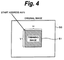
- a part of image data stored in the flash memory 32 is trimmed in a rectangular shape and transferred.
- a part of an original image 50 is trimmed as a trimming image 51 in a rectangular shape from the flash memory 32.
- the flash memory 32 is controlled so that only image data corresponding to the trimming image 51 are accessed, whereas data of an unnecessary area are not accessed.
- the trimming image 51 is designated by the overall start address of the trimming image 51, address A ST0 , and the horizontal and vertical sizes of the trimming image 51, size H and size V.
- horizontal size HALL, the start address, and the end address of the original image 50, namely addresses corresponding to data at the upper left corner and lower right corner of the original image 50 are known.
- Fig. 5 is a flow chart showing a process for trimming an image 50 and obtaining a trimming image 51 according to the embodiment of the present invention.
- data of the address A ST0 as the overall start address, size H, size V, and so forth of the trimming image 51 are set to the DMA controlling circuit 40 (at step S10). These data are supplied from an external CPU (not shown). Alternatively, these data may be supplied from the CPU 12. In addition to these data, information that designates the memory 32 of the memories 13, 22, and 32 as the flash memory 32 is supplied to the DMA controlling circuit 40.
- Data of address A STn as the start address of the next column of the trimming image 51 and the transfer size H are sent from the DMA controlling circuit 40 to the DMA device 30 at step S11.
- a start signal that causes the flash memory 32 to start transferring data is sent.
- address A ST0 which is the overall start address of the trimming image 51, is designated as address A STn .
- the DMA device 30 accesses the flash memory 32 in accordance with start address A ST0 , transfer size H, and the start signal. As a result, image data of the first column of the trimming image 51 are read from the flash memory 32. Address A ST0 of the flash memory 32 is accessed by the DMA device 30. Whenever the DMA device 30 accesses the flash memory 32, image data are successively read from address A ST0 for addresses corresponding to size H. The image data that are read are transferred to the processing circuit 41 through the bus 31. After the image data are transferred until the addresses corresponding to size H, data for one column of the trimming image 51 are transferred (at step S12).
- an end signal is sent from the DMA device 30 to the DMA controlling circuit 40 at step S13.
- the DMA controlling circuit 40 determines whether or not data for size V have been transferred (at step S14). When the determined result represents that data for size V have been transferred, since the image data of the trimming image 51 have been transferred, the process is completed.
- the flow returns to step S11. Then, the DMA controlling circuit 40 calculates address A ST1 of the start address of the next column. Assuming that the start address of the n-th column of the trimming image 51 is address A STn , address A ST(n+1) , which is the start address of the next column, is obtained by adding addresses corresponding to horizontal size H ALL of the original image 50 to address A STn .
- Whether or not the data for size V have been transferred may be determined by for example a count value for the number of cycles of the loop process returned from step S14 to step S11.
- the DMA controlling circuit 40 performs the operation for designating read widths of image data to the DMA devices 10, 20, and 30, the operation for designating the start address of the column to be subsequently read, and the operation for sending the start signal that causes the data transfer to start.
- the image processing apparatus 1 is connected to the three types of buses 11, 21, and 31 having different data bus widths.
- Dedicated DMA devices 10, 20, and 30 are disposed for the buses 11, 21, and 31, respectively.
- the DMA devices 10, 20, and 30 can share the DMA controlling circuit 40.
- the DMA devices 10, 20, and 30 commonly use the specifications for the start signal and the method for designating the address.
- the DMA controlling circuit 40 is composed of adders and registers. Thus, the circuit scale of the DMA controlling circuit 40 is relatively large. Consequently, when the DMA devices 10, 20, and 30 share the DMA controlling circuit 40, the overall circuit scale of the apparatus can be decreased.
- the interface to the DMA controlling circuit 40 is in common with the DMA devices 10, 20, and 30.
- the DMA controlling circuit 40 can equally deal with the buses 11, 21, and 31 connected to the DMA devices 10, 20, and 30, respectively.
- the DMA controlling circuit 40 can control the changed bus.
- the design of a bus can be easily changed. As a result, the design resources can be effectively reused.
- a part of an original image is trimmed in a rectangular shape and transferred for each column at a time.
- data of only a necessary portion can be transferred, a desired rectangular area can be trimmed without need to transfer data of an unnecessary data area.
- data can be transferred at high speed.
- the function for reading data for each column from a trimming image is separated from the function for controlling that function.
- controlling means for sending address information that designates to data reading means an address from which data are transferred and a start signal that causes a data transfer to start is disposed.
- a plurality of image data reading means share an interface to the controlling means.
- the controlling means can equally deal with a plurality of buses having different data bus widths. As a result, a bus can be flexibly changed.
- the design resources can be effectively reused.
Landscapes
- Engineering & Computer Science (AREA)
- Theoretical Computer Science (AREA)
- Physics & Mathematics (AREA)
- General Physics & Mathematics (AREA)
- Computer Hardware Design (AREA)
- General Engineering & Computer Science (AREA)
- Human Computer Interaction (AREA)
- Storing Facsimile Image Data (AREA)
- Image Input (AREA)
- Editing Of Facsimile Originals (AREA)
- Image Processing (AREA)
- Bus Control (AREA)
- Digital Computer Display Output (AREA)
Applications Claiming Priority (3)
| Application Number | Priority Date | Filing Date | Title |
|---|---|---|---|
| JP2002292547 | 2002-10-04 | ||
| JP2002292547A JP2004127093A (ja) | 2002-10-04 | 2002-10-04 | 画像処理装置および画像処理方法 |
| PCT/JP2003/011422 WO2004032054A1 (ja) | 2002-10-04 | 2003-09-08 | 画像処理装置および画像処理方法 |
Publications (2)
| Publication Number | Publication Date |
|---|---|
| EP1548643A1 true EP1548643A1 (de) | 2005-06-29 |
| EP1548643A4 EP1548643A4 (de) | 2008-05-14 |
Family
ID=32063919
Family Applications (1)
| Application Number | Title | Priority Date | Filing Date |
|---|---|---|---|
| EP03799097A Withdrawn EP1548643A4 (de) | 2002-10-04 | 2003-09-08 | Bildverarbeitungseinrichtung und bildverarbeitungsverfahren |
Country Status (5)
| Country | Link |
|---|---|
| US (1) | US20060050992A1 (de) |
| EP (1) | EP1548643A4 (de) |
| JP (1) | JP2004127093A (de) |
| KR (1) | KR20050052508A (de) |
| WO (1) | WO2004032054A1 (de) |
Cited By (1)
| Publication number | Priority date | Publication date | Assignee | Title |
|---|---|---|---|---|
| CN102521141A (zh) * | 2011-12-01 | 2012-06-27 | 福州瑞芯微电子有限公司 | 一种紧凑存储图像数据的读取装置及方法 |
Families Citing this family (5)
| Publication number | Priority date | Publication date | Assignee | Title |
|---|---|---|---|---|
| KR100829108B1 (ko) * | 2006-06-27 | 2008-05-16 | (주)코아정보시스템 | 패턴 기울기 계산 기능을 갖는 2차원 바코드 판독 장치 및방법 |
| KR20140109128A (ko) | 2013-03-05 | 2014-09-15 | 삼성전자주식회사 | 데이터 리드 방법과 상기 방법을 수행할 수 있는 장치들 |
| JP6476655B2 (ja) * | 2014-08-26 | 2019-03-06 | 株式会社リコー | データ転送制御装置 |
| JP2016134005A (ja) | 2015-01-20 | 2016-07-25 | オリンパス株式会社 | 画像処理装置 |
| JP6506052B2 (ja) * | 2015-03-04 | 2019-04-24 | 株式会社メガチップス | メモリデータ処理装置およびメモリデータ転送方法 |
Family Cites Families (18)
| Publication number | Priority date | Publication date | Assignee | Title |
|---|---|---|---|---|
| JPS5710067U (de) * | 1980-06-17 | 1982-01-19 | ||
| DE3141450A1 (de) * | 1980-10-17 | 1982-06-03 | Canon K.K., Tokyo | "bildverarbeitungssystem" |
| JPS58103266A (ja) * | 1981-12-15 | 1983-06-20 | Toshiba Corp | 文字画像処理装置 |
| US4574364A (en) * | 1982-11-23 | 1986-03-04 | Hitachi, Ltd. | Method and apparatus for controlling image display |
| JPS6334658A (ja) * | 1986-07-29 | 1988-02-15 | Sharp Corp | 画像処理用dmaコントロ−ラ |
| JPS63205773A (ja) * | 1987-02-20 | 1988-08-25 | Fujitsu Ltd | イメ−ジ編集方式 |
| US4907283A (en) * | 1987-03-13 | 1990-03-06 | Canon Kabushiki Kaisha | Image processing apparatus |
| JPH05193203A (ja) * | 1992-01-22 | 1993-08-03 | Toyo Electric Mfg Co Ltd | 画像矩形dma方式 |
| US5585864A (en) * | 1992-06-24 | 1996-12-17 | Seiko Epson Corporation | Apparatus for effecting high speed transfer of video data into a video memory using direct memory access |
| US5937152A (en) * | 1996-04-16 | 1999-08-10 | Brother Kogyo Kabushiki Kaisha | Printer with buffer memory |
| JPH10210251A (ja) * | 1997-01-20 | 1998-08-07 | Toshiba Corp | 画像メモリアクセス方法、画像形成装置、画像形成記憶装置、アドレス発生方法、及びアドレス発生装置 |
| US6023281A (en) * | 1998-03-02 | 2000-02-08 | Ati Technologies, Inc. | Method and apparatus for memory allocation |
| JP4098892B2 (ja) * | 1998-07-31 | 2008-06-11 | 松下電器産業株式会社 | 画像伝送装置、デジタルカメラ、画像処理装置、画像伝送方法、画像伝送方法、及び画像の有効領域指定方法 |
| JP3327900B2 (ja) * | 1999-07-12 | 2002-09-24 | 松下電器産業株式会社 | データ処理装置 |
| US6486888B1 (en) * | 1999-08-24 | 2002-11-26 | Microsoft Corporation | Alpha regions |
| US7495669B2 (en) * | 2002-12-26 | 2009-02-24 | Canon Kabushiki Kaisha | Image processing apparatus and image processing method |
| US7061642B2 (en) * | 2000-09-14 | 2006-06-13 | Canon Kabushiki Kaisha | Image processing apparatus, image processing method, storage medium, and image information printing system |
| JP3781634B2 (ja) * | 2001-04-26 | 2006-05-31 | シャープ株式会社 | 画像処理装置および画像処理方法並びに携帯用映像機器 |
-
2002
- 2002-10-04 JP JP2002292547A patent/JP2004127093A/ja active Pending
-
2003
- 2003-09-08 WO PCT/JP2003/011422 patent/WO2004032054A1/ja not_active Ceased
- 2003-09-08 EP EP03799097A patent/EP1548643A4/de not_active Withdrawn
- 2003-09-08 US US10/526,490 patent/US20060050992A1/en not_active Abandoned
- 2003-09-08 KR KR1020057004775A patent/KR20050052508A/ko not_active Ceased
Cited By (1)
| Publication number | Priority date | Publication date | Assignee | Title |
|---|---|---|---|---|
| CN102521141A (zh) * | 2011-12-01 | 2012-06-27 | 福州瑞芯微电子有限公司 | 一种紧凑存储图像数据的读取装置及方法 |
Also Published As
| Publication number | Publication date |
|---|---|
| JP2004127093A (ja) | 2004-04-22 |
| KR20050052508A (ko) | 2005-06-02 |
| US20060050992A1 (en) | 2006-03-09 |
| EP1548643A4 (de) | 2008-05-14 |
| WO2004032054A1 (ja) | 2004-04-15 |
Similar Documents
| Publication | Publication Date | Title |
|---|---|---|
| EP0584783A2 (de) | Verfahren und Vorrichtung zur verbesserten Verarbeitung | |
| EP0671718A1 (de) | Geführte Übertragung zur Zeichnung von Linien | |
| EP0525749B1 (de) | Speichersteueranordnung | |
| EP0357075A2 (de) | Datensteuerungsvorrichtung und System mit Anwendung dieser Vorrichtung | |
| EP1548643A1 (de) | Bildverarbeitungseinrichtung und bildverarbeitungsverfahren | |
| KR100758301B1 (ko) | 메모리 카드 및 그것의 데이터 저장 방법 | |
| EP0671719A1 (de) | Übertragungsprozessor mit Transparenz | |
| JPS63106848A (ja) | 制御装置 | |
| JP3683657B2 (ja) | グラフィックス表示装置およびグラフィックスプロセッサ | |
| US5333259A (en) | Graphic information processing system having a RISC CPU for displaying information in a window | |
| JPS647393Y2 (de) | ||
| JPS6334658A (ja) | 画像処理用dmaコントロ−ラ | |
| JP4137903B2 (ja) | グラフィックス表示装置およびグラフィックスプロセッサ | |
| US6567898B1 (en) | Memory controller and an information processing apparatus with improved efficiency | |
| GB2280051A (en) | Discrimination bit for DMA pointer. | |
| JP3187035B2 (ja) | メモリアクセス回路 | |
| JP3270149B2 (ja) | データ転送装置 | |
| JPH06110773A (ja) | メモリ制御装置 | |
| JPH0896112A (ja) | 画像データ処理装置およびそれを用いた情報システム | |
| US20030149804A1 (en) | Interface circuit and semiconductor device | |
| JPH01140272A (ja) | 画像処理装置 | |
| JP2003186857A (ja) | ディジタル信号処理回路 | |
| TW200805069A (en) | Memory controller | |
| JPS6165292A (ja) | グラフイツク表示装置 | |
| JPH06119289A (ja) | データ転送装置 |
Legal Events
| Date | Code | Title | Description |
|---|---|---|---|
| PUAI | Public reference made under article 153(3) epc to a published international application that has entered the european phase |
Free format text: ORIGINAL CODE: 0009012 |
|
| 17P | Request for examination filed |
Effective date: 20050405 |
|
| AK | Designated contracting states |
Kind code of ref document: A1 Designated state(s): AT BE BG CH CY CZ DE DK EE ES FI FR GB GR HU IE IT LI LU MC NL PT RO SE SI SK TR |
|
| RBV | Designated contracting states (corrected) |
Designated state(s): DE FR GB |
|
| A4 | Supplementary search report drawn up and despatched |
Effective date: 20080410 |
|
| 17Q | First examination report despatched |
Effective date: 20100111 |
|
| STAA | Information on the status of an ep patent application or granted ep patent |
Free format text: STATUS: THE APPLICATION IS DEEMED TO BE WITHDRAWN |
|
| 18D | Application deemed to be withdrawn |
Effective date: 20100401 |