EP0357075A2 - Datensteuerungsvorrichtung und System mit Anwendung dieser Vorrichtung - Google Patents
Datensteuerungsvorrichtung und System mit Anwendung dieser Vorrichtung Download PDFInfo
- Publication number
- EP0357075A2 EP0357075A2 EP89116134A EP89116134A EP0357075A2 EP 0357075 A2 EP0357075 A2 EP 0357075A2 EP 89116134 A EP89116134 A EP 89116134A EP 89116134 A EP89116134 A EP 89116134A EP 0357075 A2 EP0357075 A2 EP 0357075A2
- Authority
- EP
- European Patent Office
- Prior art keywords
- data
- bus
- peripheral device
- supplied
- request
- Prior art date
- Legal status (The legal status is an assumption and is not a legal conclusion. Google has not performed a legal analysis and makes no representation as to the accuracy of the status listed.)
- Withdrawn
Links
Images



Classifications
-
- G—PHYSICS
- G06—COMPUTING OR CALCULATING; COUNTING
- G06F—ELECTRIC DIGITAL DATA PROCESSING
- G06F13/00—Interconnection of, or transfer of information or other signals between, memories, input/output devices or central processing units
- G06F13/14—Handling requests for interconnection or transfer
-
- G—PHYSICS
- G06—COMPUTING OR CALCULATING; COUNTING
- G06F—ELECTRIC DIGITAL DATA PROCESSING
- G06F13/00—Interconnection of, or transfer of information or other signals between, memories, input/output devices or central processing units
- G06F13/14—Handling requests for interconnection or transfer
- G06F13/36—Handling requests for interconnection or transfer for access to common bus or bus system
-
- G—PHYSICS
- G06—COMPUTING OR CALCULATING; COUNTING
- G06F—ELECTRIC DIGITAL DATA PROCESSING
- G06F13/00—Interconnection of, or transfer of information or other signals between, memories, input/output devices or central processing units
- G06F13/14—Handling requests for interconnection or transfer
- G06F13/36—Handling requests for interconnection or transfer for access to common bus or bus system
- G06F13/362—Handling requests for interconnection or transfer for access to common bus or bus system with centralised access control
Definitions
- the present invention generally relates to a data control device, and particularly to a data control device such as an image display device or a direct memory access controller.
- the present invention more particularly relates to a bus arbitration for controlling requests for acquiring the right to use buses of a system, which includes a central processing unit and a data control device.
- the present invention further relates to a system which employs the above-mentioned bus arbitration.
- a system which includes a central processing unit (hereinafter referred to as a CPU), a peripheral device such as an image display device and a system memory, all of which are coupled to a bus.
- a bus arbiter is provided for controlling the right to use the bus.
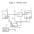
- FIG.1 there is illustrated a conventional system which includes a peripheral device 1 and a CPU 2, each of which serves as a bus mater.
- the CPU 2 is connected to a bus 5, and the peripheral device 1 is connected to the bus 5 through a buffer 4.
- a system memory 3 of large size is connected to the bus 5.
- the system memory 3 functions as a working memory for the CPU 2 and stores data and commands which are supplied to to the peripheral device 1.
- a bus arbiter 6 receives a request for acquiring the right to use the bus 5, which is generated by the peripheral device 1, and controls competition of requests for acquiring the right to use the bus 5 which are generated by the peripheral device 1 and the CPU 2.
- the peripheral device 1 needs a command or data stored in the system memory 3, it sends a request signal REQ to the bus arbiter 6.
- the bus arbiter 6 In response to the request signal REQ, the bus arbiter 6 sends the CPU 2 a hold request signal HREQ. When the CPU 2 can transfer the right to use the bus 5 to the peripheral device 1, the CPU 2 returns a hold acknowledge signal HACK to the bus arbiter 6. In response to the hold acknowledge signal HACK, the bus arbiter 6 sends an acknowledge signal ACK to the peripheral device 1. At the same time, the bus arbiter 6 outputs a gate signal to the buffer 4 so as to turn ON the buffer 4 whereby the peripheral device 1 can be connected to the bus 5. Then the peripheral device 1 obtains a command or data stored in the system memory 3 through the bus 5 and the buffer 4. When the peripheral device 1 inputs a command or data from the CPU 2, the system operates in the same manner.
- the conventional system has disadvantages described below.
- the peripheral device 1 such as an image display device needs data such as image data stored in the system memory 3
- the peripheral device 1 acquires the right to use the bus 5, and reads out image data from the system memory 3.
- a large amount of image data in a unit of kilo-words to mega-words
- efficiency in using the CPU 2 and the bus 5 is high.
- the peripheral device 1 when the peripheral device 1 needs a command, which is to be supplied from the system memory 3 or the CPU 2, the peripheral device 1 acquires the right to use the bus 5 and inputs a small amount of data related to the command (equal to a few words, for example).
- the peripheral device 1 releases the bus 5 from the exclusive use.
- the peripheral device 1 acquires the right to use the bus 5 again and inputs a small amount of data. Thereafter, the peripheral device 1 releases the bus 5 again.
- the CPU 2 must interrupts operation. Thus, efficiency in using the CPU 2 and the bus 5 is low.
- a general object of the present invention is to provide an improved peripheral device (data control device) and an improved system which uses the improved peripheral device in which the above-mentioned disadvantages are eliminated.
- a more specific object of the present invention is to provide a data control device capable of selectively using buffers based on attributes of data ("data" is a concept including commands) such as an amount of data to be transferred or a frequency in access so that a system can operate effectively and efficiently.
- data is a concept including commands
- a data control device which acquires the right to use a bus and performs data control, comprising microprogram storing means for storing microprograms, command register means for registering a command supplied from an external device, address generating means, coupled to the command register means and the microprogram storing means, for generating an address signal to be supplied to the microprogram storing means by using the command registered in the command register means, and the microprogram storing means generating control signals corresponding to one of the microprograms related to the address signal supplied from the address generating means.
- the device further comprises data processing means for processing data to be supplied from or to an external device, and request generating means, coupled to the microprogram storing means, for selectively generating a plurality of request signals for acquiring the right to use corresponding buses by using the control signals supplied from the microprogram storing means.
- the plurality of request signals are based on attributes of data to be exchanged with the external device.
- the exchanged data includes the data to be processed by the data processing means and the command to be registered in the command register means.
- Another object of the present invention is to provide a system which uses the above-mentioned data control device.
- That object of the present invention can be achieved by a data control system comprising a first bus and a second bus, data processing unit means, coupled to the first bus, for processing data to be transferred through the first bus and for generating a local request signal, and peripheral device means, coupled to the second bus, for processing data to be transferred through the second bus and for selectively generating first and second request signals for acquiring the right to use the first and second buses on the basis of attributes of the data to be transferred.
- the system further comprises first bus arbiter means, provided for the first bus, for determining whether the right to use the first bus should be given to the peripheral device means on the basis of the first request signal supplied from the peripheral device means, second bus arbiter means, provided for the second bus, for determining whether the right to use the second bus should be given to the peripheral device means or the data processing unit means on the basis of the second request signal supplied from the peripheral device means and the local request signal supplied from the processing unit means, first and second memory means, coupled to the first and second buses, for storing data to be output to the first and second buses, respectively, and buffer means, provided between the first and second buses, for preventing data on the first bus from competing with data on the second bus.
- first bus arbiter means provided for the first bus, for determining whether the right to use the first bus should be given to the peripheral device means on the basis of the first request signal supplied from the peripheral device means
- second bus arbiter means provided for the second bus, for determining whether the right to use the second bus should be given to the peripheral device means
- a data control system comprising a plurality of first buses, a second bus, data processing unit means, provided for each of the first buses and connected thereto, for processing data to be transferred through related one of the first buses and for generating a local request signal, and peripheral device means, coupled to the second bus, for processing data to be transferred through the second bus and for selectively generating a plurality of request signals for acquiring to the right to use the plurality of buses on the basis of attributes of the data to be transferred.
- the system further comprises first bus arbiter means, provided for each of the first buses, for determining whether the right to use the first bus should be given to the peripheral device means on the basis of related one of the request signals supplied from the peripheral device means, and second bus arbiter means, provided for the second bus, for determining whether the right to use the second bus should be given to the peripheral device means or the data processing unit means on the basis of the second request signal supplied from the peripheral device means and the local request signals supplied from the processing unit means.
- first bus arbiter means provided for each of the first buses, for determining whether the right to use the first bus should be given to the peripheral device means on the basis of related one of the request signals supplied from the peripheral device means
- second bus arbiter means provided for the second bus, for determining whether the right to use the second bus should be given to the peripheral device means or the data processing unit means on the basis of the second request signal supplied from the peripheral device means and the local request signals supplied from the processing unit means.
- the system comprises first memory means, coupled to each of the first buses, for storing data to be output to related one of the first buses, second memory means, coupled to the second bus, for storing data to be output to the second bus, and buffer means, provided between the second bus and each of the first buses, for preventing data on the first bus from competing with data on related one of the second buses.
- FIG.2 there is illustrated a system which includes a CPU 11 and a peripheral device 10 such as an image display device or a direct memory access controller.
- the peripheral device 10 handles a first pair of a request signal REQ1 and an acknowledge signal ACK1, and a second pair of a request signal REQ2 and an acknowledge signal ACK2.
- This structure of the peripheral device 10 is clearly distinguishable from the conventional peripheral device 1 shown in FIG.1.
- the peripheral device 10 selectively uses either the first pair or the second pair on the bases of attributes of data which are handled by the peripheral device 10.
- the CPU 11 is connected to a bus 15a, and the peripheral device 10 is connected to a bus 15b.
- a buffer 12 is interposed between the buses 15a and 15b, and is controlled by a buffer controller 16.
- the buffer 12 is formed by a bidirectional buffer.
- a system memory 13a is connected to the bus 15a, and is formed by a memory having a large storage capacity.
- the system memory 13a functions as a working memory for the CPU 11, and is capable of storing a large amount of data such as image data.
- a local memory 13b is connected to the bus 15b, and may be formed by a memory having a small storage capacity.
- the local memory 13b stores commands which are executed by the peripheral device 10.
- a bus arbiter 14a controls requests for acquiring the right to use the bus 15a.
- a bus arbiter 14b controls requests for the right to use the bus 15b.
- the first pair of the request signal REQ1 and the acknowledge signal ACK1 is transferred between the bus arbiter 14a and the peripheral device 10
- the second pair of the request signal REQ2 and the acknowledge signal ACK2 is transferred between the bus arbiter 14b and the peripheral device 10.
- the bus arbiter 14a sends the CPU 11 the aforementioned hold request signal HREQ for requesting the right to use the bus 15a to be transferred to the peripheral device 10.
- the CPU 11 returns the hold acknowledge signal HACK to the bus arbiter 14a.
- a local memory access request signal generator 17 (hereinafter simply referred to as an LMAREQ generator) supplies the bus arbiter 14b with a local memory access request signal LMAREQ when the CPU 11 generates a request for accessing the local memory 13b.
- the bus arbiter 14a generates a control signal to be supplied to a buffer controller 16 by using the request signal REQ1 and the hold acknowledge signal HACK.
- the bus arbiter 14b generates a control signal to be supplied to the buffer controller 16 by using the request signal REQ2 as well as the local memory access request signal LMAREQ.
- the bus controller 16 generates a buffer control signal from the control signals supplied from the bus arbiters 14a and 14b.
- the generated buffer control signal controls indicate whether the buffer 12 should be turned ON/OFF and indicates a direction in which data is transferred between the buses 15a and 15b.
- the peripheral device 10 When the peripheral device 10 wants to access the system memory 13a, it makes the request signal REQ1 active by switching it to a high (H) level. In response to the request signal REQ1, the bus arbiter 14a makes the hold request signal HREQ active. When the CPU 11 can transfer the right to use the bus 15a to the peripheral device 10, it makes the hold acknowledge signal HACK active. In response to the hold acknowledge signal HACK, the bus arbiter 14a makes the acknowledge signal ACK1 active. The control signal derived from the bus arbiter 14a at this time is supplied to the buffer controller 16. The hold acknowledge signal HACK is supplied to the bus arbiter 14b, which then gives the peripheral device 10 the right to use the bus 15b.
- H high
- the control signal derived from the bus arbiter 14b at this time is supplied to the bus controller 16, which generates the buffer control signal which enables data to pass through the buffer 12.
- the peripheral device 10 supplies the system memory 13a with a related address. Data related to the supplied address is read out from the system memory 13a, and transferred to the peripheral device 10 through the bus 15a, the buffer 12 and the bus 15b. Alternatively, data is supplied from the peripheral device 10 and written into the system memory 13a.
- the peripheral device 10 When the peripheral device 10 wants to access the local memory 13b and read a command therefrom, it makes the request signal REQ2 active.
- the bus arbiter 14b can give the peripheral device 10 the right to use the bus 15b, it makes the acknowledge signal ACK2 active.
- the buffer controller 16 makes the buffer 12 closed by referring to the control signal from the bus arbiter 14b. Then, a command corresponding to an address supplied from the peripheral device 10 is read out from the local memory 13b and then transferred to the peripheral device 10.
- the CPU 11 When the CPU 11 wants to access the local memory 13b and write a command therein, it controls the LMAREQ generator 17 so as to make the local memory access request signal LMAREQ active.
- the local memory access request signal LMAREQ derived from the LMAREQ generator 17 is supplied to the bus arbiter 14b.
- the acknowledge signal ACK2 is held active.
- the buffer 12 is OFF.
- data from the bus 15a is prevented from passing through the buffer 12.
- the peripheral device 10 releases the bus 15b, it makes the request signal REQ2 inactive.
- the bus arbiter 14b makes acknowledge signal ACK2 inactive.
- the buffer controller 16 turns the buffer 12 ON. Thereby, an address signal supplied from the CPU 11 is allowed to pass through the buffer 12 and supplied to the local memory 13b. Then a command derived from the CPU 11 is written into a related area in the local memory 13b.
- the CPU 11 When the CPU 11 wants to access the system memory 13a, it can use the bus 15a unless the CPU 11 keeps the hold acknowledge signal HACK active.
- the peripheral device 10 having two request signals REQ1 and REQ2 selects one of either the request signal REQ1 or REQ2 on the basis of attributes (types) of data (which is a concept including commands) to be handled. It is noted that when the peripheral device 10 needs a command, the peripheral device 10 accesses the local memory 13b, or in other words, it is unnecessary to access the system memory 13a. Thus, at this time, the operation of the CUP 11 is not interrupted.
- a system shown in FIG.3 includes an image display device 20 and a CPU 21, which correspond to the peripheral device 10 and the CPU 11 shown in FIG.2, respectively.
- the image display device 20 is connected to a buffer 30 through a local bus 28, which consists of an address bus, a data bus and a control bus.
- the buffer 30 is controlled by a buffer controller 29.
- a local memory 23, which corresponds to the local memory 13b shown in FIG.2, is connected to the local bus 28.
- the CPU 21 is connected to the buffer 30 through a system bus 27, which consists of an address bus, a data bus and a control bus.
- a system memory 22, which corresponds to the system memory 13a shown in FIG.2, is connected to the system bus 27.
- the image display device 20 can output a data request signal DREQ and a command request signal CREQ, which correspond to the request signals REQ1 and REQ2 shown in FIG.2, respectively.
- the data request signal DREQ is input directly, as a hold request signal HREQ, to the CPU 21.
- a hold acknowledge signal HACK derived from the CPU 21 is supplied directly, as a data request acknowledge signal DACK, to the image display device 20. That is, the bus arbiter 14a shown in FIG.2 is provided in the CPU 21.
- the command request signal CREQ derived from the image display device 20 is supplied to a bus arbiter 24, which corresponds to the bus arbiter 14b shown in FIG.2.
- a local memory access request (LMAREQ) generator 25 which corresponds to the LMAREQ generator 17 shown in FIG.2, generates the local memory access request signal LMAREQ, which is supplied to the bus arbiter 24.
- FIG.4A is a circuit diagram of the LMAREQ generator 25.
- the LMAREQ generator 25 is made up of an address decoder 25a, an inverter 25b and an AND gate 25c.
- the address decoder 25a is supplied with bits A22 - A31 among 32 address bits A0 - A31 supplied from the CPU 21 through the system bus 27.
- the address decoder 25a decodes the bits A22 - A31 and outputs a signal.
- the inverter 25b inverts a data strobe signal DS shown in FIG.4B, which is a low-active signal.
- the data strobe signal DS In response to this change in the data complete signal DC , the data strobe signal DS , the address strobe signal AS and the read/write signal R/ W are sequentially made inactive.
- the image display device 20 handles the signals shown in FIGS.4B(a) through 4B(e) in the same manner as the CPU 21.
- the output signals of the address decoder 25a and the inverter 25b are supplied to the AND gate 25c, which generates the local memory access request signal LMAREQ to be supplied to the bus arbiter 24.
- FIG.5 is a circuit diagram of the bus arbiter 24.
- the bus arbiter 24 is made up of an AND gate 24a having an inverter, an inverter 24b and an RS (reset/set) flip-flop 24c.
- the local memory access request signal LMAREQ from the LMAREQ generator 25 is supplied to the AND gate 24a through the inverter.
- the other input terminal of the AND gate 24 is directly supplied with the command request signal CREQ derived from the image display device 20.
- the output signal of the AND gate 24a is supplied to a set terminal of the flip-flop 24c.
- a reset terminal of the flip-flop 24c is supplied with the command request signal CREQ through the inverter 24b.
- a Q-terminal output signal of the flip-flop 24c forms the command request acknowledge signal CACK, which is to be supplied to the image display device 20.
- the command request acknowledge signal CACK is switched to 'H'.
- the command request acknowledge signal CACK is changed to 'L'.
- FIG.6 is a circuit diagram of the buffer 30 and the buffer controller 29 shown in FIG.3.
- the buffer controller 29 is made up of inverters 29a and 29e, AND gates 29b, 29c and 29f having inverters, and an NOR gate 29d.
- the buffer controller 29 is supplied with the data request acknowledge signal DACK, the local memory access request signal LMAREQ, the command request acknowledge signal CACK, and the read/write signal R/ W which is supplied from the system bus 27.
- the buffer 30 is made up of bidirectional buffers 30a, 30b, 30c and 30d, each of which has a low-active gate terminal G (having an inverter) and a direction terminal DIR.
- the gate terminal G of each of the bidirectional buffers 30a to 30d is supplied with the command request acknowledge signal CACK.
- each of the bidirectional buffer 30a to 30d When the command request acknowledge signal CACK is 'L', each of the bidirectional buffer 30a to 30d is OFF where signals are prevented from passing therethrough. On the other hand, when the command request acknowledge signal CACK is 'H', each of the bidirectional buffers 30a to 30d passes data in the direction which is specified by a signal applied to the direction terminal DIR thereof. When the direction terminal DIR is 'H', each of the bidirectional buffers 30a to 30d passes data only in the direction of A to B. On the other hand, when the direction terminal DIR is 'L', each of the bidirectional buffers 30a to 30d only passes data only in the direction of B to A. The above-mentioned operation of each bidirectional buffer is shown in the following table. Table G DIR A ⁇ B L H B ⁇ A L L OFF H X (don't care)
- the direction terminal DIR of the bidirectional buffer 30a is supplied with the data request acknowledge signal DACK through the inverter 29a.
- the signal to be supplied to the direction terminal DIR of the bidirectional buffer 30b is formed by a logic circuit consisting of the AND gates 29b, 29c having inverters and the NOR gate 29d. This logic circuit is supplied with the data request acknowledge signal DACK, the local memory access request signal LMAREQ, and the read/write signal R/ W .
- the output of the OR gate 29d is connected to the direction terminal DIR of the bidirectional buffer 30b.
- the direction terminal DIR of the bidirectional buffer 30c is supplied with the data request acknowledge signal DACK through the inverter 29e.
- the direction terminal DIR of the bidirectional buffer 30d is supplied with an output signal of the gate 29f having two inverters.
- the data request acknowledge signal DACK is supplied to the AND gate 29f through the inverter and the local memory access request signal LMAREQ is directly supplied to the AND gate 29f.
- the output signal of the AND gate 29f is supplied to the direction terminal DIR of the bidirectional buffer 30d through the inverter.
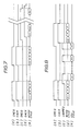
- FIG.7 A description is given of an operation of the embodiment shown in FIG.3.
- a command is input in the image display device 20 from the local memory 23 and then image data is transferred from the system memory 22 to the image display device 20.
- the image display device 20 makes the command request signal CREQ active by setting it to 'H' level. If the local memory access request signal LMAREQ is in the inactive state at this time, the bus arbiter 24 makes the command request acknowledge signal CACK active by switching it to 'H' level.
- the image display device 20 holds the data request signal DREQ 'L'.
- the bidirectional buffer 30a passes an address signal derived from the image display device 20. Then the address signal is supplied to the system memory 22 through the system bus 27.
- the image display device 20 sets the read/write signal R/ W to 'H' level. Since the signals LMAREQ and CACK are 'L' and the signals DACK and R/ W are 'H', the bidirectional buffer 30b can pass image data only in the direction of A to B.
- data D1, D2, ... are successively read out from the system memory 22 and are transferred to the image display device 20.
- the bidirectional buffer 30c passes control signals such as the address strobe signal AS and data strobe signal DS only in the B-to-A direction.
- the image display device 20 makes the data request signal DREQ inactive.
- the transferred data are stored in a display memory 26 coupled to the image display device 20.
- the first access #1 to the local memory 23 by the CPU 21 is executed. If the CPU 21 writes a command into the local memory 23, the read/write signal R/ W is set to 'L' level and thus the bidirectional buffer 30b passes this command in the A-to-B direction. On the other hand, if the CPU 21 reads a command from the local memory 23, the read/write signal R/ W is set to 'H' and thus the bidirectional buffer 30b passes this command in the B-to-A direction. Then the second and third accesses #2 and #3 to the local memory 23 are subsequently executed in the same manner.
- the image display device 20 makes the command request signal CREQ active.
- the data complete signal DC is supplied from the local memory 23 to the CPU 21 through the bidirectional buffer 30d.
- the CPU 21 controls the LMAREQ generator 25 so as to make the LMAREQ signal inactive.
- the command request acknowledge signal CACK is made active by the bus arbiter 24.
- the image display device 20 inputs the command C2 and the parameters P in the aforementioned manner.
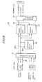
- a host bus interface circuit 31 interfaces with the CPU 21, the buffer 30, the local memory 23, and the bus arbiter 24.
- An internal address bus 36a and an internal data bus 36b extend from the host bus interface circuit 31.
- a command fetch unit 32, an image drawing unit 33 and a display unit 34 are coupled to the internal address bus 36a and the internal data bus 36b.
- the command fetch unit 32 fetches a command.
- the image drawing unit 33 draws various graphics such as a line or a curve.
- the display unit 34 controls a display device (not shown) like a CRT (cathode-ray tube) display coupled thereto through a graphic bus interface 35 so as to display graphics on the display device.
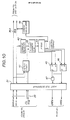
- FIG.10 is a circuit diagram of the command fetch unit 32 shown in FIG.9.
- a command fetch start circuit 41 generates an instruction to fetch a command, which activates a micro-start address programmable logic array (PLA) 43.
- the command fetch start circuit 41 is supplied with a chip select signal CS , the read/write signal R/ W and necessary information.
- a micro read only memory ( ⁇ ROM) 44 stores microprograms.
- a command register 42 temporarily stores a command supplied through the internal data bus 36b, and controls the PLA 43 so as to output an address related to the fetched command. When an address is supplied to the ⁇ ROM 44, a corresponding microprogram is read out therefrom.
- a signal derived from the ⁇ ROM 44 consists of a plurality of bits. Some of the output bits form various control signals. Two bits among the output bits are set and reset signals, which are supplied to an RS flip-flop 45. Similarly, two bits among the output bits are set and reset signals, which are supplied to an RS flip-flop 46.
- the flip-flop 45 When the address of a microprogram which requires to generate the command request signal CREQ is supplied to the ⁇ ROM 44, the flip-flop 45 is set. Since the flip-flop 46 is being reset at this time, the command request signal CREQ is derived from the Q-terminal of the flip-flop 45 and passes through an AND gate 47 and the host bus interface circuit 31. When a command which indicates the end of inputting command is stored in the command register 42, the ⁇ ROM 44 outputs the reset signal to the flip-flop 45. Thus, the command request signal CREQ is made inactive.
- the flip-flop 46 When the address of a microprogram which requires to generate the data request signal DREQ is supplied to the ⁇ ROM 44, the flip-flop 46 is set.
- the data request signal DREQ is derived from the Q-terminal of the flip-flop 46 and passes through the host bus interface circuit 31.
- the ⁇ ROM 44 When an address for a microprogram which requests to terminate inputting related data is given to the ⁇ ROM 44, the ⁇ ROM 44 outputs the reset signal to the flip-flop 46. Thus, the data request signal DREQ is made active.
- an address calculator 48 is controlled by the ⁇ ROM 44 so as to generate an address related to a desired command.
- FIG.11 A description is given of a second preferred embodiment of the present invention with reference to FIG.11.
- two CPUs 11a and 11b are provided in a system, and a peripheral device 100 can generates three request signals REQ1, REQ2 and REQ3.
- the CPU 11a, a buffer 12a, a buffer controller 16a and an LMAREQ generator 17a are the same as corresponding blocks shown in FIG.2.
- the CPU 11b is connected to a bus 15c, to which a system memory 13c is connected.
- a bus arbiter 14c controls a request for acquiring the right to use the bus 15c supplied from the peripheral device 100.
- the request signal REQ3 is supplied to the bus arbiter 14c.
- the bus arbiter 14c In response to the request signal REQ3, the bus arbiter 14c outputs the hold request signal HREQ to the CPU 11b.
- the CPU 11b may transfer the right to use the bus 15c to the peripheral device 100, the CPU 11b makes the hold acknowledge signal HACK active.
- the bus arbiter 14c makes the request acknowledge signal ACK3 active.
- a buffer 12b is interposed between the buses 15b and 15c, and is controlled by a buffer controller 16b.
- the buffer controller 16b is controlled by control signals supplied from the bus arbiters 14b and 14c in the same manner as the buffer controller 16a.
- the hold acknowledge signals HACK derived from the CPUs 11a and 11b are supplied to the bus arbiter 14b through signal lines (not shown for convenience' sake).
- the bus arbiter 14c gives the peripheral device 100 the right to use the bus 15c
- the bus arbiter 14b gives the peripheral device 100 the right to use the bus 15b in response to the hold acknowledge signal HACK supplied from the CPU 11b
Landscapes
- Engineering & Computer Science (AREA)
- Theoretical Computer Science (AREA)
- Physics & Mathematics (AREA)
- General Engineering & Computer Science (AREA)
- General Physics & Mathematics (AREA)
- Bus Control (AREA)
- Information Transfer Systems (AREA)
Applications Claiming Priority (2)
| Application Number | Priority Date | Filing Date | Title |
|---|---|---|---|
| JP218428/88 | 1988-09-02 | ||
| JP21842888 | 1988-09-02 |
Publications (2)
| Publication Number | Publication Date |
|---|---|
| EP0357075A2 true EP0357075A2 (de) | 1990-03-07 |
| EP0357075A3 EP0357075A3 (de) | 1991-12-11 |
Family
ID=16719757
Family Applications (1)
| Application Number | Title | Priority Date | Filing Date |
|---|---|---|---|
| EP19890116134 Withdrawn EP0357075A3 (de) | 1988-09-02 | 1989-08-31 | Datensteuerungsvorrichtung und System mit Anwendung dieser Vorrichtung |
Country Status (3)
| Country | Link |
|---|---|
| US (1) | US5463740A (de) |
| EP (1) | EP0357075A3 (de) |
| KR (1) | KR920010951B1 (de) |
Families Citing this family (16)
| Publication number | Priority date | Publication date | Assignee | Title |
|---|---|---|---|---|
| US5708784A (en) * | 1991-11-27 | 1998-01-13 | Emc Corporation | Dual bus computer architecture utilizing distributed arbitrators and method of using same |
| JP3524110B2 (ja) * | 1992-11-06 | 2004-05-10 | 株式会社ルネサステクノロジ | マイクロコンピュータシステム |
| US5828856A (en) * | 1994-01-28 | 1998-10-27 | Apple Computer, Inc. | Dual bus concurrent multi-channel direct memory access controller and method |
| US5619726A (en) * | 1994-10-11 | 1997-04-08 | Intel Corporation | Apparatus and method for performing arbitration and data transfer over multiple buses |
| JPH11134224A (ja) * | 1997-10-29 | 1999-05-21 | Fujitsu Ltd | 信号観測方法及び信号観測装置 |
| US6260093B1 (en) | 1998-03-31 | 2001-07-10 | Lsi Logic Corporation | Method and apparatus for arbitrating access to multiple buses in a data processing system |
| US6330622B1 (en) | 1998-10-23 | 2001-12-11 | Intel Corporation | Direct processor access via an external multi-purpose interface |
| US6339802B1 (en) * | 1999-02-19 | 2002-01-15 | International Business Machines Corporation | Computer program device and an apparatus for processing of data requests using a queued direct input-output device |
| US6519666B1 (en) * | 1999-10-05 | 2003-02-11 | International Business Machines Corporation | Arbitration scheme for optimal performance |
| JP4529063B2 (ja) * | 2001-03-30 | 2010-08-25 | ルネサスエレクトロニクス株式会社 | システムシミュレータ、シミュレーション方法及びシミュレーションプログラム |
| JP2003030018A (ja) * | 2001-07-13 | 2003-01-31 | Sony Corp | データ通信装置および方法、データ通信システム、情報処理装置および方法、記録媒体、並びにプログラム |
| US6605960B2 (en) * | 2002-01-03 | 2003-08-12 | Altera Corporation | Programmable logic configuration device with configuration memory accessible to a second device |
| US7099973B2 (en) * | 2003-03-26 | 2006-08-29 | Freescale Semiconductor, Inc. | Method and system of bus master arbitration |
| JP2006293929A (ja) * | 2005-04-14 | 2006-10-26 | Matsushita Electric Ind Co Ltd | データ伝送装置 |
| TWI278779B (en) * | 2005-09-22 | 2007-04-11 | Ours Technology Inc | Method for a controlling device commanding another controlling device |
| TWI425354B (zh) * | 2007-10-16 | 2014-02-01 | Mstar Semiconductor Inc | 資料存取系統及方法 |
Family Cites Families (22)
| Publication number | Priority date | Publication date | Assignee | Title |
|---|---|---|---|---|
| US3940743A (en) * | 1973-11-05 | 1976-02-24 | Digital Equipment Corporation | Interconnecting unit for independently operable data processing systems |
| US4130865A (en) * | 1974-06-05 | 1978-12-19 | Bolt Beranek And Newman Inc. | Multiprocessor computer apparatus employing distributed communications paths and a passive task register |
| US4257099A (en) * | 1975-10-14 | 1981-03-17 | Texas Instruments Incorporated | Communication bus coupler |
| US4041472A (en) * | 1976-04-29 | 1977-08-09 | Ncr Corporation | Data processing internal communications system having plural time-shared intercommunication buses and inter-bus communication means |
| US4205373A (en) * | 1978-05-22 | 1980-05-27 | Ncr Corporation | System and method for accessing memory connected to different bus and requesting subsystem |
| US4257095A (en) * | 1978-06-30 | 1981-03-17 | Intel Corporation | System bus arbitration, circuitry and methodology |
| US4459665A (en) * | 1979-01-31 | 1984-07-10 | Honeywell Information Systems Inc. | Data processing system having centralized bus priority resolution |
| US4300194A (en) * | 1979-01-31 | 1981-11-10 | Honeywell Information Systems Inc. | Data processing system having multiple common buses |
| US4402040A (en) * | 1980-09-24 | 1983-08-30 | Raytheon Company | Distributed bus arbitration method and apparatus |
| US4414624A (en) * | 1980-11-19 | 1983-11-08 | The United States Of America As Represented By The Secretary Of The Navy | Multiple-microcomputer processing |
| IT1151351B (it) * | 1982-01-19 | 1986-12-17 | Italtel Spa | Disposizione circuitale atta a realizzare lo scambio di dati tra una coppia di elaboratori operanti secondo il principio master-slave |
| US4470114A (en) * | 1982-03-01 | 1984-09-04 | Burroughs Corporation | High speed interconnection network for a cluster of processors |
| NL8202060A (nl) * | 1982-05-19 | 1983-12-16 | Philips Nv | Rekenmachinesysteem met een bus voor data-, adres- en besturingssignalen, welke bevat een linkerbus en een rechterbus. |
| US4590556A (en) * | 1983-01-17 | 1986-05-20 | Tandy Corporation | Co-processor combination |
| US4649471A (en) * | 1983-03-01 | 1987-03-10 | Thomson Components-Mostek Corporation | Address-controlled automatic bus arbitration and address modification |
| US4868741A (en) * | 1983-07-22 | 1989-09-19 | Texas Instruments Incorporated | Computer bus deadlock prevention |
| JPS60258671A (ja) * | 1984-06-05 | 1985-12-20 | Nec Corp | プロセツサ |
| US4729093A (en) * | 1984-09-26 | 1988-03-01 | Motorola, Inc. | Microcomputer which prioritizes instruction prefetch requests and data operand requests |
| US4897784A (en) * | 1985-06-10 | 1990-01-30 | Nay Daniel L | Multi-level bus access for multiple central processing unit |
| US4802087A (en) * | 1986-06-27 | 1989-01-31 | Honeywell Bull Inc. | Multiprocessor level change synchronization apparatus |
| JPS63132365A (ja) * | 1986-11-22 | 1988-06-04 | Nec Corp | バス調停制御方式 |
| US4837682A (en) * | 1987-04-07 | 1989-06-06 | Glen Culler & Associates | Bus arbitration system and method |
-
1989
- 1989-08-31 EP EP19890116134 patent/EP0357075A3/de not_active Withdrawn
- 1989-09-02 KR KR1019890012722A patent/KR920010951B1/ko not_active Expired
-
1995
- 1995-02-13 US US08/387,633 patent/US5463740A/en not_active Expired - Fee Related
Also Published As
| Publication number | Publication date |
|---|---|
| KR900005287A (ko) | 1990-04-13 |
| KR920010951B1 (ko) | 1992-12-24 |
| EP0357075A3 (de) | 1991-12-11 |
| US5463740A (en) | 1995-10-31 |
Similar Documents
| Publication | Publication Date | Title |
|---|---|---|
| EP0357075A2 (de) | Datensteuerungsvorrichtung und System mit Anwendung dieser Vorrichtung | |
| US5283883A (en) | Method and direct memory access controller for asynchronously reading/writing data from/to a memory with improved throughput | |
| US5119480A (en) | Bus master interface circuit with transparent preemption of a data transfer operation | |
| US6820187B2 (en) | Multiprocessor system and control method thereof | |
| JP5787629B2 (ja) | マシンビジョン用マルチプロセッサシステムオンチップ | |
| US5426737A (en) | Direct memory access for data transfer within an I/O device | |
| JP2000047974A (ja) | バス制御コントローラのバス調停方法、バス制御コントローラ及び電子機器のシステム | |
| EP0331487B1 (de) | System zur Steuerung der Datenübertragung | |
| US6195721B1 (en) | Inter-processor data transfer management | |
| US5446847A (en) | Programmable system bus priority network | |
| JP2723970B2 (ja) | データ転送制御装置 | |
| US20060050992A1 (en) | Image processing device and image processing method | |
| JP3943302B2 (ja) | プログラマブルコントローラ | |
| EP0373393A1 (de) | Informationsverarbeitungssystem | |
| JPH056333A (ja) | マルチプロセサシステム | |
| JPH03263253A (ja) | マルチプロセッサ数値制御装置 | |
| JP2002007310A (ja) | 半導体装置 | |
| JPH0320850A (ja) | 入出力制御装置 | |
| JP2000047930A (ja) | データ処理装置 | |
| JPH02168338A (ja) | データ制御装置及びこれを用いたシステム | |
| JPH06301641A (ja) | 電子計算機 | |
| JPH02222052A (ja) | ダイレクトメモリアクセス制御装置 | |
| JPH0192861A (ja) | アクセス要求認識方式 | |
| JPH034349A (ja) | Dma転送方式 | |
| KR19990057808A (ko) | 다중 억세스 캐쉬 장치 |
Legal Events
| Date | Code | Title | Description |
|---|---|---|---|
| PUAI | Public reference made under article 153(3) epc to a published international application that has entered the european phase |
Free format text: ORIGINAL CODE: 0009012 |
|
| AK | Designated contracting states |
Kind code of ref document: A2 Designated state(s): DE FR GB |
|
| PUAL | Search report despatched |
Free format text: ORIGINAL CODE: 0009013 |
|
| AK | Designated contracting states |
Kind code of ref document: A3 Designated state(s): DE FR GB |
|
| 17P | Request for examination filed |
Effective date: 19920108 |
|
| RAP1 | Party data changed (applicant data changed or rights of an application transferred) |
Owner name: FUJITSU DEVICES INC Owner name: FUJITSU LIMITED |
|
| 17Q | First examination report despatched |
Effective date: 19950321 |
|
| STAA | Information on the status of an ep patent application or granted ep patent |
Free format text: STATUS: THE APPLICATION IS DEEMED TO BE WITHDRAWN |
|
| 18D | Application deemed to be withdrawn |
Effective date: 19980303 |