EP1525621B1 - Verfahren zum Betreiben einer Halbleiteranordnung mit Graben-gate - Google Patents
Verfahren zum Betreiben einer Halbleiteranordnung mit Graben-gate Download PDFInfo
- Publication number
- EP1525621B1 EP1525621B1 EP03725542A EP03725542A EP1525621B1 EP 1525621 B1 EP1525621 B1 EP 1525621B1 EP 03725542 A EP03725542 A EP 03725542A EP 03725542 A EP03725542 A EP 03725542A EP 1525621 B1 EP1525621 B1 EP 1525621B1
- Authority
- EP
- European Patent Office
- Prior art keywords
- region
- drain
- gate
- trench
- field plate
- Prior art date
- Legal status (The legal status is an assumption and is not a legal conclusion. Google has not performed a legal analysis and makes no representation as to the accuracy of the status listed.)
- Expired - Lifetime
Links
- 239000004065 semiconductor Substances 0.000 title claims abstract description 41
- 238000000034 method Methods 0.000 title claims description 13
- 230000015556 catabolic process Effects 0.000 claims abstract description 30
- 238000005513 bias potential Methods 0.000 claims abstract description 12
- 239000000463 material Substances 0.000 claims description 3
- 238000004806 packaging method and process Methods 0.000 description 5
- 230000007704 transition Effects 0.000 description 5
- 239000011810 insulating material Substances 0.000 description 4
- 239000000758 substrate Substances 0.000 description 4
- XUIMIQQOPSSXEZ-UHFFFAOYSA-N Silicon Chemical compound [Si] XUIMIQQOPSSXEZ-UHFFFAOYSA-N 0.000 description 3
- 239000002019 doping agent Substances 0.000 description 3
- 230000005684 electric field Effects 0.000 description 3
- 239000002184 metal Substances 0.000 description 3
- 230000004048 modification Effects 0.000 description 3
- 238000012986 modification Methods 0.000 description 3
- 229910021420 polycrystalline silicon Inorganic materials 0.000 description 3
- 229910052710 silicon Inorganic materials 0.000 description 3
- 239000010703 silicon Substances 0.000 description 3
- VYPSYNLAJGMNEJ-UHFFFAOYSA-N Silicium dioxide Chemical compound O=[Si]=O VYPSYNLAJGMNEJ-UHFFFAOYSA-N 0.000 description 2
- 230000009286 beneficial effect Effects 0.000 description 2
- 238000009792 diffusion process Methods 0.000 description 2
- 238000009825 accumulation Methods 0.000 description 1
- 230000000903 blocking effect Effects 0.000 description 1
- 210000000746 body region Anatomy 0.000 description 1
- 239000003990 capacitor Substances 0.000 description 1
- 230000001413 cellular effect Effects 0.000 description 1
- 230000003247 decreasing effect Effects 0.000 description 1
- 230000005669 field effect Effects 0.000 description 1
- 238000004519 manufacturing process Methods 0.000 description 1
- 229910021421 monocrystalline silicon Inorganic materials 0.000 description 1
- 238000000059 patterning Methods 0.000 description 1
- 230000002093 peripheral effect Effects 0.000 description 1
- 230000008569 process Effects 0.000 description 1
- 230000004044 response Effects 0.000 description 1
- HBMJWWWQQXIZIP-UHFFFAOYSA-N silicon carbide Chemical compound [Si+]#[C-] HBMJWWWQQXIZIP-UHFFFAOYSA-N 0.000 description 1
- 229910010271 silicon carbide Inorganic materials 0.000 description 1
- 235000012239 silicon dioxide Nutrition 0.000 description 1
- 239000000377 silicon dioxide Substances 0.000 description 1
- 238000004088 simulation Methods 0.000 description 1
Images


Classifications
-
- H—ELECTRICITY
- H01—ELECTRIC ELEMENTS
- H01L—SEMICONDUCTOR DEVICES NOT COVERED BY CLASS H10
- H01L29/00—Semiconductor devices adapted for rectifying, amplifying, oscillating or switching, or capacitors or resistors with at least one potential-jump barrier or surface barrier, e.g. PN junction depletion layer or carrier concentration layer; Details of semiconductor bodies or of electrodes thereof ; Multistep manufacturing processes therefor
- H01L29/66—Types of semiconductor device ; Multistep manufacturing processes therefor
- H01L29/68—Types of semiconductor device ; Multistep manufacturing processes therefor controllable by only the electric current supplied, or only the electric potential applied, to an electrode which does not carry the current to be rectified, amplified or switched
- H01L29/76—Unipolar devices, e.g. field effect transistors
- H01L29/772—Field effect transistors
- H01L29/78—Field effect transistors with field effect produced by an insulated gate
- H01L29/7801—DMOS transistors, i.e. MISFETs with a channel accommodating body or base region adjoining a drain drift region
- H01L29/7802—Vertical DMOS transistors, i.e. VDMOS transistors
- H01L29/7813—Vertical DMOS transistors, i.e. VDMOS transistors with trench gate electrode, e.g. UMOS transistors
-
- H—ELECTRICITY
- H01—ELECTRIC ELEMENTS
- H01L—SEMICONDUCTOR DEVICES NOT COVERED BY CLASS H10
- H01L23/00—Details of semiconductor or other solid state devices
- H01L23/48—Arrangements for conducting electric current to or from the solid state body in operation, e.g. leads, terminal arrangements ; Selection of materials therefor
- H01L23/488—Arrangements for conducting electric current to or from the solid state body in operation, e.g. leads, terminal arrangements ; Selection of materials therefor consisting of soldered or bonded constructions
- H01L23/495—Lead-frames or other flat leads
- H01L23/49541—Geometry of the lead-frame
- H01L23/49562—Geometry of the lead-frame for devices being provided for in H01L29/00
-
- H—ELECTRICITY
- H01—ELECTRIC ELEMENTS
- H01L—SEMICONDUCTOR DEVICES NOT COVERED BY CLASS H10
- H01L23/00—Details of semiconductor or other solid state devices
- H01L23/48—Arrangements for conducting electric current to or from the solid state body in operation, e.g. leads, terminal arrangements ; Selection of materials therefor
- H01L23/488—Arrangements for conducting electric current to or from the solid state body in operation, e.g. leads, terminal arrangements ; Selection of materials therefor consisting of soldered or bonded constructions
- H01L23/495—Lead-frames or other flat leads
- H01L23/49575—Assemblies of semiconductor devices on lead frames
-
- H—ELECTRICITY
- H01—ELECTRIC ELEMENTS
- H01L—SEMICONDUCTOR DEVICES NOT COVERED BY CLASS H10
- H01L24/00—Arrangements for connecting or disconnecting semiconductor or solid-state bodies; Methods or apparatus related thereto
- H01L24/01—Means for bonding being attached to, or being formed on, the surface to be connected, e.g. chip-to-package, die-attach, "first-level" interconnects; Manufacturing methods related thereto
- H01L24/02—Bonding areas ; Manufacturing methods related thereto
- H01L24/04—Structure, shape, material or disposition of the bonding areas prior to the connecting process
- H01L24/06—Structure, shape, material or disposition of the bonding areas prior to the connecting process of a plurality of bonding areas
-
- H—ELECTRICITY
- H01—ELECTRIC ELEMENTS
- H01L—SEMICONDUCTOR DEVICES NOT COVERED BY CLASS H10
- H01L24/00—Arrangements for connecting or disconnecting semiconductor or solid-state bodies; Methods or apparatus related thereto
- H01L24/01—Means for bonding being attached to, or being formed on, the surface to be connected, e.g. chip-to-package, die-attach, "first-level" interconnects; Manufacturing methods related thereto
- H01L24/42—Wire connectors; Manufacturing methods related thereto
- H01L24/47—Structure, shape, material or disposition of the wire connectors after the connecting process
- H01L24/49—Structure, shape, material or disposition of the wire connectors after the connecting process of a plurality of wire connectors
-
- H—ELECTRICITY
- H01—ELECTRIC ELEMENTS
- H01L—SEMICONDUCTOR DEVICES NOT COVERED BY CLASS H10
- H01L29/00—Semiconductor devices adapted for rectifying, amplifying, oscillating or switching, or capacitors or resistors with at least one potential-jump barrier or surface barrier, e.g. PN junction depletion layer or carrier concentration layer; Details of semiconductor bodies or of electrodes thereof ; Multistep manufacturing processes therefor
- H01L29/40—Electrodes ; Multistep manufacturing processes therefor
- H01L29/402—Field plates
- H01L29/407—Recessed field plates, e.g. trench field plates, buried field plates
-
- H—ELECTRICITY
- H01—ELECTRIC ELEMENTS
- H01L—SEMICONDUCTOR DEVICES NOT COVERED BY CLASS H10
- H01L29/00—Semiconductor devices adapted for rectifying, amplifying, oscillating or switching, or capacitors or resistors with at least one potential-jump barrier or surface barrier, e.g. PN junction depletion layer or carrier concentration layer; Details of semiconductor bodies or of electrodes thereof ; Multistep manufacturing processes therefor
- H01L29/66—Types of semiconductor device ; Multistep manufacturing processes therefor
- H01L29/68—Types of semiconductor device ; Multistep manufacturing processes therefor controllable by only the electric current supplied, or only the electric potential applied, to an electrode which does not carry the current to be rectified, amplified or switched
- H01L29/70—Bipolar devices
- H01L29/72—Transistor-type devices, i.e. able to continuously respond to applied control signals
- H01L29/739—Transistor-type devices, i.e. able to continuously respond to applied control signals controlled by field-effect, e.g. bipolar static induction transistors [BSIT]
- H01L29/7393—Insulated gate bipolar mode transistors, i.e. IGBT; IGT; COMFET
- H01L29/7395—Vertical transistors, e.g. vertical IGBT
- H01L29/7396—Vertical transistors, e.g. vertical IGBT with a non planar surface, e.g. with a non planar gate or with a trench or recess or pillar in the surface of the emitter, base or collector region for improving current density or short circuiting the emitter and base regions
- H01L29/7397—Vertical transistors, e.g. vertical IGBT with a non planar surface, e.g. with a non planar gate or with a trench or recess or pillar in the surface of the emitter, base or collector region for improving current density or short circuiting the emitter and base regions and a gate structure lying on a slanted or vertical surface or formed in a groove, e.g. trench gate IGBT
-
- H—ELECTRICITY
- H01—ELECTRIC ELEMENTS
- H01L—SEMICONDUCTOR DEVICES NOT COVERED BY CLASS H10
- H01L29/00—Semiconductor devices adapted for rectifying, amplifying, oscillating or switching, or capacitors or resistors with at least one potential-jump barrier or surface barrier, e.g. PN junction depletion layer or carrier concentration layer; Details of semiconductor bodies or of electrodes thereof ; Multistep manufacturing processes therefor
- H01L29/66—Types of semiconductor device ; Multistep manufacturing processes therefor
- H01L29/68—Types of semiconductor device ; Multistep manufacturing processes therefor controllable by only the electric current supplied, or only the electric potential applied, to an electrode which does not carry the current to be rectified, amplified or switched
- H01L29/76—Unipolar devices, e.g. field effect transistors
- H01L29/772—Field effect transistors
- H01L29/78—Field effect transistors with field effect produced by an insulated gate
- H01L29/7801—DMOS transistors, i.e. MISFETs with a channel accommodating body or base region adjoining a drain drift region
- H01L29/7816—Lateral DMOS transistors, i.e. LDMOS transistors
- H01L29/7825—Lateral DMOS transistors, i.e. LDMOS transistors with trench gate electrode
-
- H—ELECTRICITY
- H01—ELECTRIC ELEMENTS
- H01L—SEMICONDUCTOR DEVICES NOT COVERED BY CLASS H10
- H01L2224/00—Indexing scheme for arrangements for connecting or disconnecting semiconductor or solid-state bodies and methods related thereto as covered by H01L24/00
- H01L2224/01—Means for bonding being attached to, or being formed on, the surface to be connected, e.g. chip-to-package, die-attach, "first-level" interconnects; Manufacturing methods related thereto
- H01L2224/02—Bonding areas; Manufacturing methods related thereto
- H01L2224/04—Structure, shape, material or disposition of the bonding areas prior to the connecting process
- H01L2224/05—Structure, shape, material or disposition of the bonding areas prior to the connecting process of an individual bonding area
- H01L2224/0554—External layer
- H01L2224/05599—Material
-
- H—ELECTRICITY
- H01—ELECTRIC ELEMENTS
- H01L—SEMICONDUCTOR DEVICES NOT COVERED BY CLASS H10
- H01L2224/00—Indexing scheme for arrangements for connecting or disconnecting semiconductor or solid-state bodies and methods related thereto as covered by H01L24/00
- H01L2224/01—Means for bonding being attached to, or being formed on, the surface to be connected, e.g. chip-to-package, die-attach, "first-level" interconnects; Manufacturing methods related thereto
- H01L2224/02—Bonding areas; Manufacturing methods related thereto
- H01L2224/04—Structure, shape, material or disposition of the bonding areas prior to the connecting process
- H01L2224/06—Structure, shape, material or disposition of the bonding areas prior to the connecting process of a plurality of bonding areas
- H01L2224/0601—Structure
- H01L2224/0603—Bonding areas having different sizes, e.g. different heights or widths
-
- H—ELECTRICITY
- H01—ELECTRIC ELEMENTS
- H01L—SEMICONDUCTOR DEVICES NOT COVERED BY CLASS H10
- H01L2224/00—Indexing scheme for arrangements for connecting or disconnecting semiconductor or solid-state bodies and methods related thereto as covered by H01L24/00
- H01L2224/01—Means for bonding being attached to, or being formed on, the surface to be connected, e.g. chip-to-package, die-attach, "first-level" interconnects; Manufacturing methods related thereto
- H01L2224/42—Wire connectors; Manufacturing methods related thereto
- H01L2224/47—Structure, shape, material or disposition of the wire connectors after the connecting process
- H01L2224/48—Structure, shape, material or disposition of the wire connectors after the connecting process of an individual wire connector
- H01L2224/481—Disposition
- H01L2224/48135—Connecting between different semiconductor or solid-state bodies, i.e. chip-to-chip
- H01L2224/48137—Connecting between different semiconductor or solid-state bodies, i.e. chip-to-chip the bodies being arranged next to each other, e.g. on a common substrate
-
- H—ELECTRICITY
- H01—ELECTRIC ELEMENTS
- H01L—SEMICONDUCTOR DEVICES NOT COVERED BY CLASS H10
- H01L2224/00—Indexing scheme for arrangements for connecting or disconnecting semiconductor or solid-state bodies and methods related thereto as covered by H01L24/00
- H01L2224/01—Means for bonding being attached to, or being formed on, the surface to be connected, e.g. chip-to-package, die-attach, "first-level" interconnects; Manufacturing methods related thereto
- H01L2224/42—Wire connectors; Manufacturing methods related thereto
- H01L2224/47—Structure, shape, material or disposition of the wire connectors after the connecting process
- H01L2224/48—Structure, shape, material or disposition of the wire connectors after the connecting process of an individual wire connector
- H01L2224/481—Disposition
- H01L2224/48151—Connecting between a semiconductor or solid-state body and an item not being a semiconductor or solid-state body, e.g. chip-to-substrate, chip-to-passive
- H01L2224/48221—Connecting between a semiconductor or solid-state body and an item not being a semiconductor or solid-state body, e.g. chip-to-substrate, chip-to-passive the body and the item being stacked
- H01L2224/48245—Connecting between a semiconductor or solid-state body and an item not being a semiconductor or solid-state body, e.g. chip-to-substrate, chip-to-passive the body and the item being stacked the item being metallic
- H01L2224/48247—Connecting between a semiconductor or solid-state body and an item not being a semiconductor or solid-state body, e.g. chip-to-substrate, chip-to-passive the body and the item being stacked the item being metallic connecting the wire to a bond pad of the item
-
- H—ELECTRICITY
- H01—ELECTRIC ELEMENTS
- H01L—SEMICONDUCTOR DEVICES NOT COVERED BY CLASS H10
- H01L2224/00—Indexing scheme for arrangements for connecting or disconnecting semiconductor or solid-state bodies and methods related thereto as covered by H01L24/00
- H01L2224/01—Means for bonding being attached to, or being formed on, the surface to be connected, e.g. chip-to-package, die-attach, "first-level" interconnects; Manufacturing methods related thereto
- H01L2224/42—Wire connectors; Manufacturing methods related thereto
- H01L2224/47—Structure, shape, material or disposition of the wire connectors after the connecting process
- H01L2224/49—Structure, shape, material or disposition of the wire connectors after the connecting process of a plurality of wire connectors
- H01L2224/491—Disposition
- H01L2224/4911—Disposition the connectors being bonded to at least one common bonding area, e.g. daisy chain
- H01L2224/49111—Disposition the connectors being bonded to at least one common bonding area, e.g. daisy chain the connectors connecting two common bonding areas, e.g. Litz or braid wires
-
- H—ELECTRICITY
- H01—ELECTRIC ELEMENTS
- H01L—SEMICONDUCTOR DEVICES NOT COVERED BY CLASS H10
- H01L2224/00—Indexing scheme for arrangements for connecting or disconnecting semiconductor or solid-state bodies and methods related thereto as covered by H01L24/00
- H01L2224/01—Means for bonding being attached to, or being formed on, the surface to be connected, e.g. chip-to-package, die-attach, "first-level" interconnects; Manufacturing methods related thereto
- H01L2224/42—Wire connectors; Manufacturing methods related thereto
- H01L2224/47—Structure, shape, material or disposition of the wire connectors after the connecting process
- H01L2224/49—Structure, shape, material or disposition of the wire connectors after the connecting process of a plurality of wire connectors
- H01L2224/491—Disposition
- H01L2224/4912—Layout
- H01L2224/49171—Fan-out arrangements
-
- H—ELECTRICITY
- H01—ELECTRIC ELEMENTS
- H01L—SEMICONDUCTOR DEVICES NOT COVERED BY CLASS H10
- H01L2224/00—Indexing scheme for arrangements for connecting or disconnecting semiconductor or solid-state bodies and methods related thereto as covered by H01L24/00
- H01L2224/80—Methods for connecting semiconductor or other solid state bodies using means for bonding being attached to, or being formed on, the surface to be connected
- H01L2224/85—Methods for connecting semiconductor or other solid state bodies using means for bonding being attached to, or being formed on, the surface to be connected using a wire connector
- H01L2224/8538—Bonding interfaces outside the semiconductor or solid-state body
- H01L2224/85399—Material
-
- H—ELECTRICITY
- H01—ELECTRIC ELEMENTS
- H01L—SEMICONDUCTOR DEVICES NOT COVERED BY CLASS H10
- H01L24/00—Arrangements for connecting or disconnecting semiconductor or solid-state bodies; Methods or apparatus related thereto
- H01L24/01—Means for bonding being attached to, or being formed on, the surface to be connected, e.g. chip-to-package, die-attach, "first-level" interconnects; Manufacturing methods related thereto
- H01L24/42—Wire connectors; Manufacturing methods related thereto
- H01L24/47—Structure, shape, material or disposition of the wire connectors after the connecting process
- H01L24/48—Structure, shape, material or disposition of the wire connectors after the connecting process of an individual wire connector
-
- H—ELECTRICITY
- H01—ELECTRIC ELEMENTS
- H01L—SEMICONDUCTOR DEVICES NOT COVERED BY CLASS H10
- H01L25/00—Assemblies consisting of a plurality of individual semiconductor or other solid state devices ; Multistep manufacturing processes thereof
- H01L25/16—Assemblies consisting of a plurality of individual semiconductor or other solid state devices ; Multistep manufacturing processes thereof the devices being of types provided for in two or more different main groups of groups H01L27/00 - H01L33/00, or in a single subclass of H10K, H10N, e.g. forming hybrid circuits
-
- H—ELECTRICITY
- H01—ELECTRIC ELEMENTS
- H01L—SEMICONDUCTOR DEVICES NOT COVERED BY CLASS H10
- H01L29/00—Semiconductor devices adapted for rectifying, amplifying, oscillating or switching, or capacitors or resistors with at least one potential-jump barrier or surface barrier, e.g. PN junction depletion layer or carrier concentration layer; Details of semiconductor bodies or of electrodes thereof ; Multistep manufacturing processes therefor
- H01L29/40—Electrodes ; Multistep manufacturing processes therefor
- H01L29/41—Electrodes ; Multistep manufacturing processes therefor characterised by their shape, relative sizes or dispositions
- H01L29/423—Electrodes ; Multistep manufacturing processes therefor characterised by their shape, relative sizes or dispositions not carrying the current to be rectified, amplified or switched
- H01L29/42312—Gate electrodes for field effect devices
- H01L29/42316—Gate electrodes for field effect devices for field-effect transistors
- H01L29/4232—Gate electrodes for field effect devices for field-effect transistors with insulated gate
-
- H—ELECTRICITY
- H01—ELECTRIC ELEMENTS
- H01L—SEMICONDUCTOR DEVICES NOT COVERED BY CLASS H10
- H01L29/00—Semiconductor devices adapted for rectifying, amplifying, oscillating or switching, or capacitors or resistors with at least one potential-jump barrier or surface barrier, e.g. PN junction depletion layer or carrier concentration layer; Details of semiconductor bodies or of electrodes thereof ; Multistep manufacturing processes therefor
- H01L29/66—Types of semiconductor device ; Multistep manufacturing processes therefor
- H01L29/68—Types of semiconductor device ; Multistep manufacturing processes therefor controllable by only the electric current supplied, or only the electric potential applied, to an electrode which does not carry the current to be rectified, amplified or switched
- H01L29/76—Unipolar devices, e.g. field effect transistors
- H01L29/772—Field effect transistors
- H01L29/78—Field effect transistors with field effect produced by an insulated gate
- H01L29/7827—Vertical transistors
- H01L29/7828—Vertical transistors without inversion channel, e.g. vertical ACCUFETs, normally-on vertical MISFETs
-
- H—ELECTRICITY
- H01—ELECTRIC ELEMENTS
- H01L—SEMICONDUCTOR DEVICES NOT COVERED BY CLASS H10
- H01L2924/00—Indexing scheme for arrangements or methods for connecting or disconnecting semiconductor or solid-state bodies as covered by H01L24/00
- H01L2924/0001—Technical content checked by a classifier
- H01L2924/00014—Technical content checked by a classifier the subject-matter covered by the group, the symbol of which is combined with the symbol of this group, being disclosed without further technical details
-
- H—ELECTRICITY
- H01—ELECTRIC ELEMENTS
- H01L—SEMICONDUCTOR DEVICES NOT COVERED BY CLASS H10
- H01L2924/00—Indexing scheme for arrangements or methods for connecting or disconnecting semiconductor or solid-state bodies as covered by H01L24/00
- H01L2924/01—Chemical elements
- H01L2924/01005—Boron [B]
-
- H—ELECTRICITY
- H01—ELECTRIC ELEMENTS
- H01L—SEMICONDUCTOR DEVICES NOT COVERED BY CLASS H10
- H01L2924/00—Indexing scheme for arrangements or methods for connecting or disconnecting semiconductor or solid-state bodies as covered by H01L24/00
- H01L2924/01—Chemical elements
- H01L2924/01014—Silicon [Si]
-
- H—ELECTRICITY
- H01—ELECTRIC ELEMENTS
- H01L—SEMICONDUCTOR DEVICES NOT COVERED BY CLASS H10
- H01L2924/00—Indexing scheme for arrangements or methods for connecting or disconnecting semiconductor or solid-state bodies as covered by H01L24/00
- H01L2924/01—Chemical elements
- H01L2924/01015—Phosphorus [P]
-
- H—ELECTRICITY
- H01—ELECTRIC ELEMENTS
- H01L—SEMICONDUCTOR DEVICES NOT COVERED BY CLASS H10
- H01L2924/00—Indexing scheme for arrangements or methods for connecting or disconnecting semiconductor or solid-state bodies as covered by H01L24/00
- H01L2924/01—Chemical elements
- H01L2924/01033—Arsenic [As]
-
- H—ELECTRICITY
- H01—ELECTRIC ELEMENTS
- H01L—SEMICONDUCTOR DEVICES NOT COVERED BY CLASS H10
- H01L2924/00—Indexing scheme for arrangements or methods for connecting or disconnecting semiconductor or solid-state bodies as covered by H01L24/00
- H01L2924/01—Chemical elements
- H01L2924/01082—Lead [Pb]
-
- H—ELECTRICITY
- H01—ELECTRIC ELEMENTS
- H01L—SEMICONDUCTOR DEVICES NOT COVERED BY CLASS H10
- H01L2924/00—Indexing scheme for arrangements or methods for connecting or disconnecting semiconductor or solid-state bodies as covered by H01L24/00
- H01L2924/10—Details of semiconductor or other solid state devices to be connected
- H01L2924/11—Device type
- H01L2924/12—Passive devices, e.g. 2 terminal devices
- H01L2924/1203—Rectifying Diode
- H01L2924/12036—PN diode
-
- H—ELECTRICITY
- H01—ELECTRIC ELEMENTS
- H01L—SEMICONDUCTOR DEVICES NOT COVERED BY CLASS H10
- H01L2924/00—Indexing scheme for arrangements or methods for connecting or disconnecting semiconductor or solid-state bodies as covered by H01L24/00
- H01L2924/10—Details of semiconductor or other solid state devices to be connected
- H01L2924/11—Device type
- H01L2924/13—Discrete devices, e.g. 3 terminal devices
- H01L2924/1304—Transistor
- H01L2924/1305—Bipolar Junction Transistor [BJT]
- H01L2924/13055—Insulated gate bipolar transistor [IGBT]
-
- H—ELECTRICITY
- H01—ELECTRIC ELEMENTS
- H01L—SEMICONDUCTOR DEVICES NOT COVERED BY CLASS H10
- H01L2924/00—Indexing scheme for arrangements or methods for connecting or disconnecting semiconductor or solid-state bodies as covered by H01L24/00
- H01L2924/10—Details of semiconductor or other solid state devices to be connected
- H01L2924/11—Device type
- H01L2924/13—Discrete devices, e.g. 3 terminal devices
- H01L2924/1304—Transistor
- H01L2924/1306—Field-effect transistor [FET]
- H01L2924/13091—Metal-Oxide-Semiconductor Field-Effect Transistor [MOSFET]
-
- H—ELECTRICITY
- H01—ELECTRIC ELEMENTS
- H01L—SEMICONDUCTOR DEVICES NOT COVERED BY CLASS H10
- H01L2924/00—Indexing scheme for arrangements or methods for connecting or disconnecting semiconductor or solid-state bodies as covered by H01L24/00
- H01L2924/19—Details of hybrid assemblies other than the semiconductor or other solid state devices to be connected
- H01L2924/1901—Structure
- H01L2924/1904—Component type
- H01L2924/19041—Component type being a capacitor
-
- H—ELECTRICITY
- H01—ELECTRIC ELEMENTS
- H01L—SEMICONDUCTOR DEVICES NOT COVERED BY CLASS H10
- H01L2924/00—Indexing scheme for arrangements or methods for connecting or disconnecting semiconductor or solid-state bodies as covered by H01L24/00
- H01L2924/30—Technical effects
- H01L2924/301—Electrical effects
- H01L2924/3025—Electromagnetic shielding
Landscapes
- Engineering & Computer Science (AREA)
- Microelectronics & Electronic Packaging (AREA)
- Power Engineering (AREA)
- Computer Hardware Design (AREA)
- Physics & Mathematics (AREA)
- Condensed Matter Physics & Semiconductors (AREA)
- General Physics & Mathematics (AREA)
- Ceramic Engineering (AREA)
- Electrodes Of Semiconductors (AREA)
- Insulated Gate Type Field-Effect Transistor (AREA)
Claims (7)
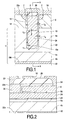
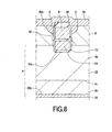
- Ein Verfahren zum Betreiben einer Halbleitervorrichtung mit Graben-Gate, wobei die Halbleitervorrichtung mit Graben-Gate aufweist:einen Halbleiterkörper (20), der einen Graben (10) definiert, der ein isoliertes Gate (8) darin aufweist, wobei der Halbleiterkörper einen Source-Bereich (2) und einen Drain-Bereich (4) eines ersten Leitfähigskeitstyps aufweist, die durch einen Kanalaufnehmungsbereich (6) angrenzend an das Gate getrennt sind, wobei der Drain-Bereich einen Drain-Driftbereich (4a) und einen Drain-Kontaktbereich (4b) aufweist, mit dem Drain-Driftbereich zwischen dem Kanalaufnehmungsbereich (6) und dem Drain-Kontaktbereich (4b), und wobei der Drain-Driftbereich (4a) in geringerem Maße dotiert ist als der Drain-Kontaktbereich (4b); undeine isolierte Feldplatte (24) in dem Graben zwischen dem Gate (8) und dem Drain-Kontaktbereich (4b);wobei das Verfahren gekennzeichnet ist durch Verbinden der Feldplatte (24) mit einem Vorspannungspotential größer als das Gate-Potential und nahe der Bulk-Durchbruchspannung des Drain-Driftbereichs (4a), wobei die Bulk-Durchbruchspannung die Maximalspannung pro Mikrometer ist, die ohne Lawinendurchbruch durch einen einseitigen abrupten 1D pn-Übergang, der unter Verwendung von Halbleitermaterial des Drain-Driftbereichs (4a) bei Raumtemperatur gebildet wird, ausgehalten wird.
- Das Verfahren gemäß Anspruch 1, wobei der Graben (10) sich im Wesentlichen zu dem Übergang (4c) zwischen dem Drain-Driftbereich (4a) und dem Drain-Kontaktbereich (4b) erstreckt.
- Das Verfahren gemäß Anspruch 1 oder 2, wobei das Gate (8) flacher als die obere Grenze des Drain-Driftbereichs (4a) angrenzend an den Graben (10) ist, und die Feldplatte (24) sich über die obere Grenze erstreckt.
- Das Verfahren gemäß einem der vorhergehenden Ansprüche, wobei die Vorrichtung in einem Modul (60) enthalten ist und wobei die Feldplatte (24) mit einer internen Spannungsleitung des Moduls (60) verbunden ist.
- Das Verfahren gemäß einem der vorhergehenden Ansprüche, wobei ein zusätzlicher externer Anschluss (54) vorgesehen ist, der elektrisch mit der Feldplatte (24) verbunden ist.
- Das Verfahren gemäß einem der vorhergehenden Ansprüche, wobei das Vorspannungspotential ungefähr 60 bis 100% der Bulk-Durchbruchspannung des Drain-Driftbereichs (4a) ist.
- Ein Verfahren gemäß Anspruch 6, wobei das Vorspannungspotential ungefähr 80% der Bulk-Durchbruchspannung des Drain-Driftbereichs (4a) ist.
Applications Claiming Priority (5)
| Application Number | Priority Date | Filing Date | Title |
|---|---|---|---|
| GBGB0212564.9A GB0212564D0 (en) | 2002-05-31 | 2002-05-31 | Trench-gate semiconductor device |
| GB0212564 | 2002-05-31 | ||
| GB0228809 | 2002-12-11 | ||
| GBGB0228809.0A GB0228809D0 (en) | 2002-05-31 | 2002-12-11 | Trench-gate semiconductor devices |
| PCT/IB2003/002233 WO2003103056A2 (en) | 2002-05-31 | 2003-05-21 | Trench-gate semiconductor device,corresponding module and apparatus ,and method of operating the device |
Publications (2)
| Publication Number | Publication Date |
|---|---|
| EP1525621A2 EP1525621A2 (de) | 2005-04-27 |
| EP1525621B1 true EP1525621B1 (de) | 2011-10-12 |
Family
ID=29713387
Family Applications (1)
| Application Number | Title | Priority Date | Filing Date |
|---|---|---|---|
| EP03725542A Expired - Lifetime EP1525621B1 (de) | 2002-05-31 | 2003-05-21 | Verfahren zum Betreiben einer Halbleiteranordnung mit Graben-gate |
Country Status (5)
| Country | Link |
|---|---|
| US (1) | US7122860B2 (de) |
| EP (1) | EP1525621B1 (de) |
| JP (1) | JP2005528804A (de) |
| AU (1) | AU2003228073A1 (de) |
| WO (1) | WO2003103056A2 (de) |
Families Citing this family (43)
| Publication number | Priority date | Publication date | Assignee | Title |
|---|---|---|---|---|
| US7638841B2 (en) * | 2003-05-20 | 2009-12-29 | Fairchild Semiconductor Corporation | Power semiconductor devices and methods of manufacture |
| DE10339455B3 (de) * | 2003-08-27 | 2005-05-04 | Infineon Technologies Ag | Vertikales Halbleiterbauelement mit einer eine Feldelektrode aufweisenden Driftzone und Verfahren zur Herstellung einer solchen Driftzone |
| GB0327792D0 (en) * | 2003-11-29 | 2003-12-31 | Koninkl Philips Electronics Nv | Trench insulated gate field effect transistor |
| TWI222685B (en) * | 2003-12-18 | 2004-10-21 | Episil Technologies Inc | Metal oxide semiconductor device and fabricating method thereof |
| US7405452B2 (en) * | 2004-02-02 | 2008-07-29 | Hamza Yilmaz | Semiconductor device containing dielectrically isolated PN junction for enhanced breakdown characteristics |
| US20050199918A1 (en) * | 2004-03-15 | 2005-09-15 | Daniel Calafut | Optimized trench power MOSFET with integrated schottky diode |
| JP2005340626A (ja) * | 2004-05-28 | 2005-12-08 | Toshiba Corp | 半導体装置 |
| DE102004029435B4 (de) * | 2004-06-18 | 2017-02-16 | Infineon Technologies Ag | Feldplattentrenchtransistor |
| JP5259920B2 (ja) * | 2004-08-04 | 2013-08-07 | ローム株式会社 | 半導体装置およびその製造方法 |
| DE102004044619B4 (de) * | 2004-09-13 | 2009-07-16 | Infineon Technologies Ag | Kondensatorstruktur in Grabenstrukturen von Halbleiterbauteilen und Halbleiterbauteile mit derartigen Kondensatorstrukturen und Verfahren zur Herstellung derselben |
| DE112006000832B4 (de) | 2005-04-06 | 2018-09-27 | Fairchild Semiconductor Corporation | Trenched-Gate-Feldeffekttransistoren und Verfahren zum Bilden derselben |
| JP4955222B2 (ja) | 2005-05-20 | 2012-06-20 | ルネサスエレクトロニクス株式会社 | 半導体装置の製造方法 |
| AT504289A2 (de) | 2005-05-26 | 2008-04-15 | Fairchild Semiconductor | Trench-gate-feldeffekttransistoren und verfahren zum bilden derselben |
| US7446374B2 (en) * | 2006-03-24 | 2008-11-04 | Fairchild Semiconductor Corporation | High density trench FET with integrated Schottky diode and method of manufacture |
| DE102006026943B4 (de) * | 2006-06-09 | 2011-01-05 | Infineon Technologies Austria Ag | Mittels Feldeffekt steuerbarer Trench-Transistor mit zwei Steuerelektroden |
| DE102006030631B4 (de) * | 2006-07-03 | 2011-01-05 | Infineon Technologies Austria Ag | Halbleiterbauelementanordnung mit einem Leistungsbauelement und einem Logikbauelement |
| US7476932B2 (en) * | 2006-09-29 | 2009-01-13 | The Boeing Company | U-shape metal-oxide-semiconductor (UMOS) gate structure for high power MOS-based semiconductor devices |
| US8497549B2 (en) * | 2007-08-21 | 2013-07-30 | Fairchild Semiconductor Corporation | Method and structure for shielded gate trench FET |
| JP2009164558A (ja) * | 2007-12-10 | 2009-07-23 | Toyota Central R&D Labs Inc | 半導体装置とその製造方法、並びにトレンチゲートの製造方法 |
| US20100013009A1 (en) * | 2007-12-14 | 2010-01-21 | James Pan | Structure and Method for Forming Trench Gate Transistors with Low Gate Resistance |
| US7800176B2 (en) * | 2008-10-27 | 2010-09-21 | Infineon Technologies Austria Ag | Electronic circuit for controlling a power field effect transistor |
| US8198678B2 (en) * | 2009-12-09 | 2012-06-12 | Infineon Technologies Austria Ag | Semiconductor device with improved on-resistance |
| JP6008377B2 (ja) * | 2010-03-03 | 2016-10-19 | ルネサスエレクトロニクス株式会社 | Pチャネル型パワーmosfet |
| JP5674530B2 (ja) * | 2010-09-10 | 2015-02-25 | ルネサスエレクトロニクス株式会社 | 半導体装置の制御装置 |
| JP2012204636A (ja) * | 2011-03-25 | 2012-10-22 | Toshiba Corp | 半導体装置およびその製造方法 |
| US8981748B2 (en) | 2011-08-08 | 2015-03-17 | Semiconductor Components Industries, Llc | Method of forming a semiconductor power switching device, structure therefor, and power converter |
| US8642425B2 (en) | 2012-05-29 | 2014-02-04 | Semiconductor Components Industries, Llc | Method of making an insulated gate semiconductor device and structure |
| US9735241B2 (en) * | 2013-05-16 | 2017-08-15 | Infineon Technologies Americas Corp. | Semiconductor device with a field plate double trench having a thick bottom dielectric |
| JP2015142073A (ja) * | 2014-01-30 | 2015-08-03 | サンケン電気株式会社 | 半導体装置 |
| US9413348B2 (en) | 2014-07-29 | 2016-08-09 | Semiconductor Components Industries, Llc | Electronic circuit including a switch having an associated breakdown voltage and a method of using the same |
| JP2016063048A (ja) * | 2014-09-17 | 2016-04-25 | 富士電機株式会社 | トレンチ型絶縁ゲートバイポーラトランジスタ及びその製造方法 |
| JP2016163019A (ja) * | 2015-03-05 | 2016-09-05 | 株式会社東芝 | 半導体装置 |
| CN107636836B (zh) * | 2015-12-11 | 2020-11-27 | 富士电机株式会社 | 半导体装置 |
| DE102016103587B4 (de) * | 2016-02-29 | 2020-12-03 | Infineon Technologies Ag | Halbleitervorrichtung mit Hilfselektrodenpins |
| JP6830390B2 (ja) * | 2017-03-28 | 2021-02-17 | エイブリック株式会社 | 半導体装置 |
| JP7250473B2 (ja) * | 2018-10-18 | 2023-04-03 | 三菱電機株式会社 | 半導体装置 |
| FR3096832B1 (fr) | 2019-05-28 | 2022-05-13 | St Microelectronics Rousset | Structure de transistor |
| FR3106697A1 (fr) * | 2020-01-23 | 2021-07-30 | Stmicroelectronics (Rousset) Sas | Structure de transistor |
| EP4197026A4 (de) * | 2020-08-13 | 2023-10-11 | Texas Instruments Incorporated | Halbleiterbauelement mit seitlichem isolator |
| JP2023539108A (ja) * | 2020-08-19 | 2023-09-13 | 華為技術有限公司 | DrMOS、集積回路、電子機器、及び製造方法 |
| CN112349786B (zh) * | 2020-11-06 | 2022-07-29 | 中国电子科技集团公司第二十四研究所 | 介质共用的电阻场板场效应mos器件及其制备方法 |
| EP4167292A1 (de) * | 2021-10-15 | 2023-04-19 | Infineon Technologies Dresden GmbH & Co . KG | Halbleiterbauelement |
| CN114709258B (zh) * | 2022-06-07 | 2022-08-30 | 深圳市威兆半导体股份有限公司 | 一种双沟道mosfet器件及其制造方法 |
Family Cites Families (7)
| Publication number | Priority date | Publication date | Assignee | Title |
|---|---|---|---|---|
| US5998833A (en) * | 1998-10-26 | 1999-12-07 | North Carolina State University | Power semiconductor devices having improved high frequency switching and breakdown characteristics |
| JP2003525003A (ja) | 1999-07-02 | 2003-08-19 | コーニンクレッカ フィリップス エレクトロニクス エヌ ヴィ | Dc−dcコンバータ用スイッチング装置及びスイッチコンポーネント |
| EP1170803A3 (de) * | 2000-06-08 | 2002-10-09 | Siliconix Incorporated | MOSFET mit Graben-Gateelektrode und Verfahren zu dessen Herstellung |
| DE10038177A1 (de) * | 2000-08-04 | 2002-02-21 | Infineon Technologies Ag | Mittels Feldeffekt steuerbares Halbleiterschaltelement mit zwei Steuerelektroden |
| DE10212149B4 (de) | 2002-03-19 | 2007-10-04 | Infineon Technologies Ag | Transistoranordnung mit Schirmelektrode außerhalb eines aktiven Zellenfeldes und reduzierter Gate-Drain-Kapazität |
| DE10214175B4 (de) * | 2002-03-28 | 2006-06-29 | Infineon Technologies Ag | Mittels Feldeffekt steuerbares Halbleiterbauelement und Verfahren zu dessen Herstellung |
| EP1514300A1 (de) * | 2002-05-31 | 2005-03-16 | Koninklijke Philips Electronics N.V. | Halbleiteranornung mit graben-gateelektrode und herstellungsverfahren |
-
2003
- 2003-05-21 EP EP03725542A patent/EP1525621B1/de not_active Expired - Lifetime
- 2003-05-21 JP JP2004510038A patent/JP2005528804A/ja not_active Withdrawn
- 2003-05-21 AU AU2003228073A patent/AU2003228073A1/en not_active Abandoned
- 2003-05-21 WO PCT/IB2003/002233 patent/WO2003103056A2/en active Application Filing
- 2003-05-21 US US10/515,748 patent/US7122860B2/en not_active Expired - Lifetime
Also Published As
| Publication number | Publication date |
|---|---|
| WO2003103056A3 (en) | 2004-02-05 |
| AU2003228073A1 (en) | 2003-12-19 |
| JP2005528804A (ja) | 2005-09-22 |
| US20050173758A1 (en) | 2005-08-11 |
| US7122860B2 (en) | 2006-10-17 |
| AU2003228073A8 (en) | 2003-12-19 |
| WO2003103056A2 (en) | 2003-12-11 |
| EP1525621A2 (de) | 2005-04-27 |
Similar Documents
| Publication | Publication Date | Title |
|---|---|---|
| EP1525621B1 (de) | Verfahren zum Betreiben einer Halbleiteranordnung mit Graben-gate | |
| US7232726B2 (en) | Trench-gate semiconductor device and method of manufacturing | |
| US7719053B2 (en) | Semiconductor device having increased gate-source capacity provided by protruding electrode disposed between gate electrodes formed in a trench | |
| US8193570B2 (en) | Synchronous buck converter using shielded gate field effect transistors | |
| US6710403B2 (en) | Dual trench power MOSFET | |
| US6388286B1 (en) | Power semiconductor devices having trench-based gate electrodes and field plates | |
| US8344448B2 (en) | Semiconductor device having an edge termination structure and method of manufacture thereof | |
| CN111712926B (zh) | 碳化硅半导体装置 | |
| US9252263B1 (en) | Multiple semiconductor device trenches per cell pitch | |
| US20100327348A1 (en) | Semiconductor device, method of manufacturing the same and power-supply device using the same | |
| EP0494597A1 (de) | Leistungshalbleiteranordnung mit einer Graben-Gateelektrode | |
| US7423325B2 (en) | Lateral field-effect-controllable semiconductor component for RF applications | |
| EP1870940A1 (de) | Halbleiterbauelement | |
| KR20050006283A (ko) | 트렌치-게이트 반도체 디바이스와 그의 작동 방법 및트렌치-게이트 반도체 디바이스를 포함하는 모듈 및 장치 | |
| WO2005045938A2 (en) | Insulated gate field-effect transistor | |
| CN116031303B (zh) | 超结器件及其制作方法和电子器件 | |
| CN113497133A (zh) | 半导体装置以及半导体电路 | |
| US7554157B2 (en) | Lateral SOI component having a reduced on resistance | |
| JP7472068B2 (ja) | 半導体装置及び半導体回路 | |
| US7642596B2 (en) | Insulated gate field effect transistor | |
| WO2006038201A2 (en) | Power semiconductor device and corresponding circuit | |
| CN117425965A (zh) | 碳化硅半导体装置 |
Legal Events
| Date | Code | Title | Description |
|---|---|---|---|
| PUAI | Public reference made under article 153(3) epc to a published international application that has entered the european phase |
Free format text: ORIGINAL CODE: 0009012 |
|
| 17P | Request for examination filed |
Effective date: 20050103 |
|
| AK | Designated contracting states |
Kind code of ref document: A2 Designated state(s): AT BE BG CH CY CZ DE DK EE ES FI FR GB GR HU IE IT LI LU MC NL PT RO SE SI SK TR |
|
| AX | Request for extension of the european patent |
Extension state: AL LT LV MK |
|
| DAX | Request for extension of the european patent (deleted) | ||
| RAP1 | Party data changed (applicant data changed or rights of an application transferred) |
Owner name: NXP B.V. |
|
| 17Q | First examination report despatched |
Effective date: 20091116 |
|
| GRAP | Despatch of communication of intention to grant a patent |
Free format text: ORIGINAL CODE: EPIDOSNIGR1 |
|
| RIC1 | Information provided on ipc code assigned before grant |
Ipc: H01L 29/40 20060101ALI20110523BHEP Ipc: H01L 29/78 20060101AFI20110523BHEP Ipc: H01L 25/07 20060101ALN20110523BHEP Ipc: H01L 29/739 20060101ALI20110523BHEP |
|
| RTI1 | Title (correction) |
Free format text: METHOD OF OPERATING A TRENCH GATE SEMICONDUCTOR DEVICE |
|
| RIN1 | Information on inventor provided before grant (corrected) |
Inventor name: RUTTER, PHILIP Inventor name: GROVER, RAYMOND J. Inventor name: PEAKE, STEVEN T. |
|
| GRAS | Grant fee paid |
Free format text: ORIGINAL CODE: EPIDOSNIGR3 |
|
| GRAA | (expected) grant |
Free format text: ORIGINAL CODE: 0009210 |
|
| AK | Designated contracting states |
Kind code of ref document: B1 Designated state(s): AT BE BG CH CY CZ DE DK EE ES FI FR GB GR HU IE IT LI LU MC NL PT RO SE SI SK TR |
|
| REG | Reference to a national code |
Ref country code: GB Ref legal event code: FG4D |
|
| REG | Reference to a national code |
Ref country code: DE Ref legal event code: R081 Ref document number: 60338736 Country of ref document: DE Owner name: NEXPERIA B.V., NL Free format text: FORMER OWNER: KONINKLIJKE PHILIPS ELECTRONICS N.V., EINDHOVEN, NL |
|
| REG | Reference to a national code |
Ref country code: CH Ref legal event code: EP |
|
| REG | Reference to a national code |
Ref country code: IE Ref legal event code: FG4D |
|
| REG | Reference to a national code |
Ref country code: DE Ref legal event code: R096 Ref document number: 60338736 Country of ref document: DE Effective date: 20111201 |
|
| REG | Reference to a national code |
Ref country code: NL Ref legal event code: VDEP Effective date: 20111012 |
|
| REG | Reference to a national code |
Ref country code: AT Ref legal event code: MK05 Ref document number: 528799 Country of ref document: AT Kind code of ref document: T Effective date: 20111012 |
|
| PG25 | Lapsed in a contracting state [announced via postgrant information from national office to epo] |
Ref country code: BE Free format text: LAPSE BECAUSE OF FAILURE TO SUBMIT A TRANSLATION OF THE DESCRIPTION OR TO PAY THE FEE WITHIN THE PRESCRIBED TIME-LIMIT Effective date: 20111012 |
|
| PG25 | Lapsed in a contracting state [announced via postgrant information from national office to epo] |
Ref country code: PT Free format text: LAPSE BECAUSE OF FAILURE TO SUBMIT A TRANSLATION OF THE DESCRIPTION OR TO PAY THE FEE WITHIN THE PRESCRIBED TIME-LIMIT Effective date: 20120213 Ref country code: GR Free format text: LAPSE BECAUSE OF FAILURE TO SUBMIT A TRANSLATION OF THE DESCRIPTION OR TO PAY THE FEE WITHIN THE PRESCRIBED TIME-LIMIT Effective date: 20120113 Ref country code: SI Free format text: LAPSE BECAUSE OF FAILURE TO SUBMIT A TRANSLATION OF THE DESCRIPTION OR TO PAY THE FEE WITHIN THE PRESCRIBED TIME-LIMIT Effective date: 20111012 Ref country code: SE Free format text: LAPSE BECAUSE OF FAILURE TO SUBMIT A TRANSLATION OF THE DESCRIPTION OR TO PAY THE FEE WITHIN THE PRESCRIBED TIME-LIMIT Effective date: 20111012 Ref country code: NL Free format text: LAPSE BECAUSE OF FAILURE TO SUBMIT A TRANSLATION OF THE DESCRIPTION OR TO PAY THE FEE WITHIN THE PRESCRIBED TIME-LIMIT Effective date: 20111012 |
|
| PG25 | Lapsed in a contracting state [announced via postgrant information from national office to epo] |
Ref country code: CY Free format text: LAPSE BECAUSE OF FAILURE TO SUBMIT A TRANSLATION OF THE DESCRIPTION OR TO PAY THE FEE WITHIN THE PRESCRIBED TIME-LIMIT Effective date: 20111012 |
|
| PG25 | Lapsed in a contracting state [announced via postgrant information from national office to epo] |
Ref country code: EE Free format text: LAPSE BECAUSE OF FAILURE TO SUBMIT A TRANSLATION OF THE DESCRIPTION OR TO PAY THE FEE WITHIN THE PRESCRIBED TIME-LIMIT Effective date: 20111012 Ref country code: SK Free format text: LAPSE BECAUSE OF FAILURE TO SUBMIT A TRANSLATION OF THE DESCRIPTION OR TO PAY THE FEE WITHIN THE PRESCRIBED TIME-LIMIT Effective date: 20111012 Ref country code: DK Free format text: LAPSE BECAUSE OF FAILURE TO SUBMIT A TRANSLATION OF THE DESCRIPTION OR TO PAY THE FEE WITHIN THE PRESCRIBED TIME-LIMIT Effective date: 20111012 Ref country code: BG Free format text: LAPSE BECAUSE OF FAILURE TO SUBMIT A TRANSLATION OF THE DESCRIPTION OR TO PAY THE FEE WITHIN THE PRESCRIBED TIME-LIMIT Effective date: 20120112 Ref country code: CZ Free format text: LAPSE BECAUSE OF FAILURE TO SUBMIT A TRANSLATION OF THE DESCRIPTION OR TO PAY THE FEE WITHIN THE PRESCRIBED TIME-LIMIT Effective date: 20111012 |
|
| PLBE | No opposition filed within time limit |
Free format text: ORIGINAL CODE: 0009261 |
|
| STAA | Information on the status of an ep patent application or granted ep patent |
Free format text: STATUS: NO OPPOSITION FILED WITHIN TIME LIMIT |
|
| PG25 | Lapsed in a contracting state [announced via postgrant information from national office to epo] |
Ref country code: IT Free format text: LAPSE BECAUSE OF FAILURE TO SUBMIT A TRANSLATION OF THE DESCRIPTION OR TO PAY THE FEE WITHIN THE PRESCRIBED TIME-LIMIT Effective date: 20111012 Ref country code: RO Free format text: LAPSE BECAUSE OF FAILURE TO SUBMIT A TRANSLATION OF THE DESCRIPTION OR TO PAY THE FEE WITHIN THE PRESCRIBED TIME-LIMIT Effective date: 20111012 |
|
| 26N | No opposition filed |
Effective date: 20120713 |
|
| REG | Reference to a national code |
Ref country code: DE Ref legal event code: R097 Ref document number: 60338736 Country of ref document: DE Effective date: 20120713 |
|
| PG25 | Lapsed in a contracting state [announced via postgrant information from national office to epo] |
Ref country code: MC Free format text: LAPSE BECAUSE OF NON-PAYMENT OF DUE FEES Effective date: 20120531 |
|
| REG | Reference to a national code |
Ref country code: CH Ref legal event code: PL |
|
| PG25 | Lapsed in a contracting state [announced via postgrant information from national office to epo] |
Ref country code: AT Free format text: LAPSE BECAUSE OF FAILURE TO SUBMIT A TRANSLATION OF THE DESCRIPTION OR TO PAY THE FEE WITHIN THE PRESCRIBED TIME-LIMIT Effective date: 20111012 Ref country code: LI Free format text: LAPSE BECAUSE OF NON-PAYMENT OF DUE FEES Effective date: 20120531 Ref country code: CH Free format text: LAPSE BECAUSE OF NON-PAYMENT OF DUE FEES Effective date: 20120531 |
|
| REG | Reference to a national code |
Ref country code: IE Ref legal event code: MM4A |
|
| PG25 | Lapsed in a contracting state [announced via postgrant information from national office to epo] |
Ref country code: IE Free format text: LAPSE BECAUSE OF NON-PAYMENT OF DUE FEES Effective date: 20120521 Ref country code: ES Free format text: LAPSE BECAUSE OF FAILURE TO SUBMIT A TRANSLATION OF THE DESCRIPTION OR TO PAY THE FEE WITHIN THE PRESCRIBED TIME-LIMIT Effective date: 20120123 |
|
| PG25 | Lapsed in a contracting state [announced via postgrant information from national office to epo] |
Ref country code: FI Free format text: LAPSE BECAUSE OF FAILURE TO SUBMIT A TRANSLATION OF THE DESCRIPTION OR TO PAY THE FEE WITHIN THE PRESCRIBED TIME-LIMIT Effective date: 20111012 |
|
| PG25 | Lapsed in a contracting state [announced via postgrant information from national office to epo] |
Ref country code: TR Free format text: LAPSE BECAUSE OF FAILURE TO SUBMIT A TRANSLATION OF THE DESCRIPTION OR TO PAY THE FEE WITHIN THE PRESCRIBED TIME-LIMIT Effective date: 20111012 |
|
| PG25 | Lapsed in a contracting state [announced via postgrant information from national office to epo] |
Ref country code: LU Free format text: LAPSE BECAUSE OF NON-PAYMENT OF DUE FEES Effective date: 20120521 |
|
| PG25 | Lapsed in a contracting state [announced via postgrant information from national office to epo] |
Ref country code: HU Free format text: LAPSE BECAUSE OF FAILURE TO SUBMIT A TRANSLATION OF THE DESCRIPTION OR TO PAY THE FEE WITHIN THE PRESCRIBED TIME-LIMIT Effective date: 20030521 |
|
| REG | Reference to a national code |
Ref country code: FR Ref legal event code: PLFP Year of fee payment: 14 |
|
| REG | Reference to a national code |
Ref country code: DE Ref legal event code: R081 Ref document number: 60338736 Country of ref document: DE Owner name: NEXPERIA B.V., NL Free format text: FORMER OWNER: NXP B.V., EINDHOVEN, NL |
|
| REG | Reference to a national code |
Ref country code: GB Ref legal event code: 732E Free format text: REGISTERED BETWEEN 20161013 AND 20161019 |
|
| REG | Reference to a national code |
Ref country code: FR Ref legal event code: TP Owner name: NEXPERIA B.V., NL Effective date: 20161109 |
|
| REG | Reference to a national code |
Ref country code: FR Ref legal event code: PLFP Year of fee payment: 15 |
|
| PGFP | Annual fee paid to national office [announced via postgrant information from national office to epo] |
Ref country code: DE Payment date: 20170530 Year of fee payment: 15 Ref country code: FR Payment date: 20170516 Year of fee payment: 15 Ref country code: GB Payment date: 20170530 Year of fee payment: 15 |
|
| REG | Reference to a national code |
Ref country code: DE Ref legal event code: R119 Ref document number: 60338736 Country of ref document: DE |
|
| GBPC | Gb: european patent ceased through non-payment of renewal fee |
Effective date: 20180521 |
|
| PG25 | Lapsed in a contracting state [announced via postgrant information from national office to epo] |
Ref country code: DE Free format text: LAPSE BECAUSE OF NON-PAYMENT OF DUE FEES Effective date: 20181201 Ref country code: GB Free format text: LAPSE BECAUSE OF NON-PAYMENT OF DUE FEES Effective date: 20180521 Ref country code: FR Free format text: LAPSE BECAUSE OF NON-PAYMENT OF DUE FEES Effective date: 20180531 |