EP1517217A2 - Schnittstellenschaltung und Taktausgabeverfahren dazu - Google Patents
Schnittstellenschaltung und Taktausgabeverfahren dazu Download PDFInfo
- Publication number
- EP1517217A2 EP1517217A2 EP04255663A EP04255663A EP1517217A2 EP 1517217 A2 EP1517217 A2 EP 1517217A2 EP 04255663 A EP04255663 A EP 04255663A EP 04255663 A EP04255663 A EP 04255663A EP 1517217 A2 EP1517217 A2 EP 1517217A2
- Authority
- EP
- European Patent Office
- Prior art keywords
- data
- clock signal
- clock
- circuit
- level
- Prior art date
- Legal status (The legal status is an assumption and is not a legal conclusion. Google has not performed a legal analysis and makes no representation as to the accuracy of the status listed.)
- Granted
Links
Images





Classifications
-
- H—ELECTRICITY
- H04—ELECTRIC COMMUNICATION TECHNIQUE
- H04L—TRANSMISSION OF DIGITAL INFORMATION, e.g. TELEGRAPHIC COMMUNICATION
- H04L12/00—Data switching networks
- H04L12/02—Details
-
- G—PHYSICS
- G06—COMPUTING OR CALCULATING; COUNTING
- G06F—ELECTRIC DIGITAL DATA PROCESSING
- G06F1/00—Details not covered by groups G06F3/00 - G06F13/00 and G06F21/00
- G06F1/04—Generating or distributing clock signals or signals derived directly therefrom
-
- H—ELECTRICITY
- H04—ELECTRIC COMMUNICATION TECHNIQUE
- H04L—TRANSMISSION OF DIGITAL INFORMATION, e.g. TELEGRAPHIC COMMUNICATION
- H04L12/00—Data switching networks
- H04L12/28—Data switching networks characterised by path configuration, e.g. LAN [Local Area Networks] or WAN [Wide Area Networks]
- H04L12/40—Bus networks
-
- H—ELECTRICITY
- H04—ELECTRIC COMMUNICATION TECHNIQUE
- H04L—TRANSMISSION OF DIGITAL INFORMATION, e.g. TELEGRAPHIC COMMUNICATION
- H04L7/00—Arrangements for synchronising receiver with transmitter
Definitions
- the presentinvention relates to aninterface circuit and a clock output method for the interface circuit.
- Apparatus sets such as car audio and home audio have a plurality of data processing circuits for data processing associated with audio incorporated therein. These data processing circuits are connected in parallel via a controller such as a microcomputer and buses as needed, and by the controller supplying data, each of them executes data processing synchronously with data processing being executed by the other data processing circuits.
- a controller such as a microcomputer and buses as needed, and by the controller supplying data, each of them executes data processing synchronously with data processing being executed by the other data processing circuits.
- FIG. 9 is a block diagram for explaining a data processing system comprising a plurality of data processing circuits and a controller.
- the plurality of data processing circuits include, but not limited to, a PLL (Phase Locked Loop), an LCD (Liquid Crystal Display) driver, a DSP (Digital Signal Processor), an FM multiple receive circuit.
- PLL Phase Locked Loop
- LCD Liquid Crystal Display
- DSP Digital Signal Processor
- the PLL 4, LCD driver 6, DSP 8, and FM multiple receive circuit 10 are connected to the controller 2 via a data bus DB1 for transmitting a control signal CE, a data bus DB2 for transmitting a clock signal CL (or clock CL), a data bus DB3 for transmitting data DI, and a data bus DB3 for transmitting data DO as needed.
- the controller 2 outputs control signal CL, clock CL, and data DI to the PLL 4, LCD driver 6, DSP 8, and FM multiple receive circuit 10. Also, the controller 2 has data DO from the PLL 4, LCD driver 6, DSP 8, or FM multiple receive circuit 10 inputted therein while outputting control signal CE and clock CL.
- the PLL 4, LCD driver 6, DSP 8, or FM multiple receive circuit 10 may not be connected to the controller 2 via data bus DB4. In this embodiment, for example, the controller 2 and the LCD driver 6 are not connected via data bus DB4.
- the PLL 4 is for executing tuning of an electronic tuner, and has an interface circuit 4A that performs data input/output with the controller 2 and a data register 4B that holds data output from the interface circuit 4A.
- the LCD driver 6 is for executing frequency display processing for the electronic tuner, and has an interface circuit 6A that receives data input from the controller 2 and a data register 6B that holds data output from the interface circuit 6A.
- the DSP 8 is for executing digital processing on audio data, for example, and has an interface circuit 8A that performs data input/output with the controller 2 and a data register 8B that holds data output from the interface circuit 8A.
- the FM multiple receive circuit 10 is for decoding FM-multiple, superposed data, and has an interface circuit 10A that performs data input/output with the controller 2 and a data register 10B that holds data output from the interface circuit 10A.
- FIG. 10 is a circuit diagram showing an example of the interface circuit.
- FIG. 11 is a time chart for explaining the operation of the interface circuit of FIG. 10. Note that the interface circuit of FIG. 10 does not have data bus DB4 for outputting data DO to the controller 2.
- the interface circuit has control signal CE, clock CL, and data DI inputted therein, and outputs clock SCL and data SDI.
- the interface circuit comprises an AND gate 102 and an AND gate 104 (clock output circuit).
- the AND gate 102 outputs data DI as data SDI depending on the level of control signal CE. That is, the AND gate 102 closes when control signal CE is at "L” (low level), and opens and outputs data DI as data SDI when control signal CE is at "H” (high level).
- the AND gate 104 outputs clock CL as clock SCL depending on the level of control signal CE. That is, when control signal CE is at "L”, the AND gate 104 closes and, when control signal CE is at "H”, opens and outputs clock CL as clock SCL.
- the controller 2 holds clock CL at “L” and lets data DI be indefinite when control signal CE is at “L”.
- the controller 2 outputs clock CL and data DI synchronous with the clock CL when control signal CE is at "H”. That is, when control signal CE is at "L”, the AND gate 102 outputs data SDI of "L” and the AND gate 104 outputs clock SCL of "L”.
- the AND gate 102 outputs data SDI that is the same as data DI and the AND gate 104 outputs clock SCL that is the same as clock CL.
- the data register serially reads in data SDI synchronously with clock SCL and holds the data.
- the data processing circuit performs required data processing on the bit value held in the data register. Note that when outputting clock CL and data DI, the controller 2 has to enable a data processing circuit as a target and disable the other data processing circuits, which are not a target. Hence, the program processing load of the controller 2 itself is large.
- FIG. 13 is a circuit diagram showing another example of the interface circuit.
- FIG. 14 is a time chart for explaining the operation of the interface circuit of FIG. 13. Note that the interface circuit of FIG. 13 does not have data bus DB4 for outputting data DO to the controller 2.
- the interface circuit of FIG. 13 identifies a data processing circuit as a target with hardware, thereby reducing the program processing load of the controller 2 itself.
- the PLL 4, LCD driver 6, DSP 8, and FM multiple receive circuit 10 have respective intrinsic address codes to identify them.
- control signal CE When control signal CE is at "L”, the controller 2 outputs clock CL and data DI (address code A0 to A7) synchronous therewith, and when control signal CE is at "H”, the controller 2 outputs clock CL and data DI (data D0 to Dn-1) synchronous therewith and subsequent to data DI (address code A0 to A7).
- control signal CE is at "L”
- the controller 2 holds clock CL at “L” except while data DI (address code A0 to A7) is output, and that the address code is not limited to an 8-bit code.
- the interface circuit has control signal CE, clock CL, and data DI inputted therein, and outputs clock SCL and data SDI.
- the interface circuit comprises an address register 202, an address decoder 204, a delay circuit 206, an inverter 208, an AND gate 210, an OR gate 212, a D flip-flop 214, an AND gate 216, and an AND gate 218 (clock output circuit).
- the address register 202 serially reads in data DI (address code A0 to A7) at the rise timings of clock CL.
- the address decoder 204 checks whether the 8-bit address code A0 to A7 inputted in the address register 202 matches the intrinsic address code, and when both match, outputs "H", for example.
- the address decoder 204 is hardware including a PLA (Programmable Logic Array), logic gates and the like.
- the OR gate 212 outputs "L” only for the delay time of the delay circuit 206 after the change point of control signal CE from “H” to “L”.
- the AND gate 210 outputs "H” only for the delay time of the delay circuit 206 after the change point of control signal CE from "L” to “H”.
- the D flip-flop 214 is reset at the change point of control signal CE from "H” to "L”, and at the change point of control signal CE from "L” to “H”, reads in and holds the decode output of the address decoder 204 with outputting data EN, which is the same as the decode output.
- the D flip-flop 214 outputs data EN of "H".
- the AND gate 216 outputs data DI (data D0 to Dn-1) as data SDI depending on the level of data EN. That is, when data EN is at "L”, the AND gate 216 closes, and when data EN is at "H”, opens and outputs data DI (data D0 to Dn-1) as data SDI.
- the AND gate 218 outputs clock CL as clock SCL depending on the levels of control signal CE and data EN. That is, when either control signal CE or data EN is at “L”, the AND gate 218 closes, and when control signal CE and data EN are at “H”, opens and outputs clock CL as clock SCL.
- controllers 2 when stopping clock CL, some controllers 2 hold clock CL at "L” while the others hold clock CL at "H".
- FIG. 11 is a time chart for explaining the operation of the interface circuit of FIG. 10 for the specification that the controller 2 holds clock CL at "L”.
- FIG. 12 is a time chart for explaining the operation of the interface circuit of FIG. 10 for the specification that the controller 2 holds clock CL at "H”.
- the AND gate 104 outputs one clock (dummy clock) at a timing just before the AND gate 102 outputs data DO, and thereby the data register may read in data of "L” before data DO and hold it, thus causing wrong data processing by the data processing circuit.
- FIG. 14 is a time chart for explaining the operation of the interface circuit of FIG. 13 for the specification that the controller 2 holds clock CL at "L”.
- FIG. 15 is a time chart for explaining the operation of the interface circuit of FIG. 13 for the specification that the controller 2 holds clock CL at "H”.
- the AND gate 216 outputs address code A7 just before data DO and the AND gate 218 outputs one clock (dummy clock) at a timing while the AND gate 216 outputs address code A7, and thereby the data register may read in address code A7, thus causing wrong data processing by the data processing circuit.
- An object of the present invention is to provide an interface circuit.
- One aspect of the present invention to solve the above problems is an interface circuit which outputs a clock signal and data to a data register that serially reads in the data synchronously with the clock signal, in response to a control signal changing from one level to the other level, for outputting the clock signal and the data
- the interface circuit comprising a clock output circuit that, responding to the level of the clock signal when the control signal changes from the one level to the other level, outputs clocks of the clock signal that are the same in number as bits of the data to the data register.
- This interface circuit outputs appropriate data to the data register at appropriate timings.
- the interface circuit is reduced in circuit size and cost.
- circuit size is prevented from becoming large and data processing is ensured.
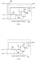
- FIG. 1 is a circuit diagram for explaining an example of the interface circuit of the present invention.
- FIG. 2 is a circuit diagram for explaining a modified example of the interface circuit of FIG. 1.
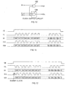
- FIG. 3 is a time chart for explaining the operation of the interface circuit of FIG. 1 for the specification that the controller 2 holds clock CL at "L”.
- FIG. 4 is a time chart for explaining the operation of the interface circuit of FIG. 1 for the specification that the controller 2 holds clock CL at "H”. Note that the interface circuit of FIG. 1 does not have data bus DB4 for outputting data DO to the controller 2.
- the controller 2 holds clock CL at “L” and lets data DI be indefinite when control signal CE is at “L”.
- the controller 2 outputs clock CL and data DI synchronous with the clock CL when control signal CE is at "H”.
- the interface circuit has control signal CE, clock CL, and data DI inputted therein, and outputs clock SCL and data SDI.
- the interface circuit comprises an AND gate 302 (data output circuit) and a logic circuit 304 (clock output circuit).
- the AND gate 302 outputs data DI as data SDI depending on the level of control signal CE. That is, the AND gate 302 closes when control signal CE is at "L”, and opens and outputs data DI as data SDI when control signal CE is at "H".
- the logic circuit 304 outputs clock CL as clock SCL depending on the level of control signal CE.
- the logic circuit 304 comprises an inverter 306, an AND gate 308, a latch circuit 310, and an AND gate 312 (gate circuit).
- the inverter 306 outputs inverted clock /CL with respect to clock CL.
- the AND gate 308 outputs inverted clock /CL as latch clock LCL depending on the level of control signal CE. That is, when control signal CE is at "L”, the AND gate 308 closes and, when control signal CE is at "H”, opens and outputs inverted clock /CL as latch clock LCL.
- the latch circuit 310 latches a voltage V of "H” (data for allowing the output of clock SCL) in response to a level change of latch clock LCL and outputs as data SCLEN. Specifically, at the timing when latch clock LCL rises from “L” to “H”, that is, when control signal CE becomes “H” and clock CL becomes “L”, the latch circuit 310 latches the voltage V and outputs data SCLEN of "H”. Note that when control signal CE is at "L”, the latch circuit 310 is reset to output data SCLEN of "L”.
- the AND gate 312 outputs clock CL as clock SCL depending on the levels of control signal CE and data SCLEN. That is, when either control signal CE or data SCLEN is at “L”, the AND gate 312 closes and, when control signal CE and data SCLEN are at "H", opens and outputs clock CL as clock SCL.
- a logic circuit 314 of FIG. 2 is a circuit that can replace the logic circuit 304 of FIG. 1. Note that the same reference numerals denote the same elements as in FIG. 1 with a description thereof omitted.
- An AND gate 316 outputs clock CL as clock SCL depending on the level of data SCLEN. That is, when data SCLEN is at "L”, the AND gate 316 closes and, when data SCLEN is at "H”, opens and outputs clock CL as clock SCL.
- the logic circuit 314 does not need a signal line for supplying control signal CE to the AND gate 316. That is, when an interface circuit having the logic circuit 314 is integrated in a chip, that signal line need not be drawn on the chip, thus reducing the influence of noise due to, e.g., modulated waves and reducing the integrated circuit in size.
- control signal CE When control signal CE is at "L", the AND gate 302 outputs data SDI of "L". At this time, because the latch circuit 310 is reset, the AND gate 312 outputs clock SCL of "L".
- control signal CE rises from “L” to “H"
- control signal CE is at "H”
- clock CL stays at “L”.
- the AND gate 308 outputs latch clock LCL rising to "H”
- the reset of the latch circuit 310 is negated, and thus the latch circuit 310 latches the voltage V at the timing when latch clock LCL rises to "H” and outputs data SCLEN of "H".
- control signal CE When control signal CE is at "H", the AND gate 302 outputs data SDI that is the same as data DI. At this time, because the voltage V is latched in the latch circuit 310, the AND gate 312 outputs clock SCL that is the same as clock CL.
- control signal CE When control signal CE is at "L", the AND gate 302 outputs data SDI of "L". At this time, because the latch circuit 310 is reset, the AND gate 312 outputs clock SCL of "L".
- control signal CE When control signal CE is at "H", the AND gate 302 outputs data SDI that is the same as data DI. Further, when control signal CE and data SCLEN are at "H”, i.e. the voltage V is latched in the latch circuit 310, the AND gate 312 outputs clock SCL that is the same as clock CL.
- the controller 2 when outputting clock CL and data DI, the controller 2 enables a data processing circuit as a target and disables the other data processing circuits, which are not a target.
- FIG. 5 is a circuit diagram explaining another example of the interface circuit.
- FIG. 6 is a circuit diagram for explaining a modified example of the interface circuit of FIG. 5.
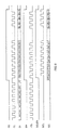
- FIG. 7 is a time chart for explaining the operation of the interface circuit of FIG. 5 for the specification that the controller 2 holds clock CL at "L”.
- FIG. 8 is a time chart for explaining the operation of the interface circuit of FIG. 5 for the specification that the controller 2 holds clock CL at "H”. Note that the interface circuit of FIG. 5 does not have data bus DB4 for outputting data DO to the controller 2 and identifies a data processing circuit as a target with hardware.
- the PLL 4, LCD driver 6, DSP 8, and FM multiple receive circuit 10 have respective intrinsic address codes to identify them.
- control signal CE When control signal CE is at "L”, the controller 2 outputs clock CL and data DI (address code A0 to A7) synchronous therewith, and when control signal CE is at "H”, the controller 2 outputs clock CL and data DI (data D0 to Dn-1) synchronous therewith and subsequent to data DI (address code A0 to A7).
- control signal CE is at "L”
- the controller 2 holds clock CL at "L” (FIG. 7) or "H” (FIG. 8) except while data DI (address code A0 to A7) is output, and that the address code is not limited to an 8-bit code.
- the interface circuit has control signal CE, clock CL, and data DI inputted therein, and outputs clock SCL and data SDI.
- the interface circuit comprises an address register 402, an address decoder 404, a delay circuit 406, an inverter 408, an AND gate 410, an OR gate 412, a D flip-flop 414, an AND gate 416 (data output circuit), and a logic circuit 418 (clock output circuit).
- the address register 402 serially reads in data DI (address code A0 to A7) at the rise timings of clock CL.
- the address decoder 404 checks whether the 8-bit address code A0 to A7 inputted in the address register 402 matches the preset intrinsic address code, and when both match, outputs "H", for example.
- the address decoder 404 is hardware including a PLA (Programmable Logic Array), logic gates and the like.
- the OR gate 412 outputs "L” only for the delay time of the delay circuit 406 after the change point of control signal CE from “H” to “L”.
- the AND gate 410 outputs "H” only for the delay time of the delay circuit 406 after the change point of control signal CE from "L” to “H”.
- the D flip-flop 414 is reset at the change point of control signal CE from “H” to "L”, and at the change point of control signal CE from "L” to “H”, reads in and holds the decode output of the address decoder 404 with outputting data EN, which is the same as the decode output.
- the D flip-flop 214 outputs data EN of "H".
- the AND gate 416 outputs data DI (data D0 to Dn-1) as data SDI depending on the level of data EN. That is, when data EN is at "L”, the AND gate 416 closes, and when data EN is at "H", opens and outputs data DI (data D0 to Dn-1) as data SDI.
- the logic circuit 418 outputs clock CL as clock SCL depending on the levels of control signal CE and data EN.
- the logic circuit 418 comprises an inverter 420, an AND gate 422, a latch circuit 424, and an AND gate 426 (gate circuit).
- the inverter 420 outputs inverted clock /CL with respect to clock CL.
- the AND gate 422 outputs inverted clock /CL as latch clock LCL depending on the level of data EN. That is, when data EN is at "L”, the AND gate 422 closes and, when data EN is at "H”, opens and outputs inverted clock /CL as latch clock LCL.
- the latch circuit 424 latches a voltage V of "H” (data for allowing the output of clock SCL) in response to a level change of latch clock LCL and outputs as data SCLEN. Specifically, at the timing when latch clock LCL rises from “L” to “H”, that is, when data EN changes from “L” to “H” and clock CL changes from “H” to “L”, the latch circuit 424 latches the voltage V and outputs data SCLEN of "H”. Note that when data EN is at “L”, the latch circuit 424 is reset to output data SCLEN of "L”.
- the AND gate 426 outputs clock CL as clock SCL depending on the levels of control signal CE and data SCLEN. That is, when either control signal CE or data SCLEN is at “L” , the AND gate 426 closes and, when control signal CE and data SCLEN are at "H”, opens and outputs clock CL as clock SCL.
- a logic circuit 428 of FIG. 6 is a circuit that can replace the logic circuit 418 of FIG. 5. Note that in FIG. 6, the same reference numerals denote the same elements as in FIG. 5 with a description thereof omitted.
- An AND gate 430 outputs clock CL as clock SCL depending on the level of data SCLEN. That is, when data SCLEN is at "L”, the AND gate 430 closes and, when data SCLEN is at "H”, opens and outputs clock CL as clock SCL.
- the logic circuit 428 does not need a signal line for supplying control signal CE to the AND gate 430. That is, when an interface circuit having the logic circuit 428 is integrated in a chip, that signal line need not be drawn on the chip, thus reducing the influence of noise due to, e.g., modulated waves and reducing the integrated circuit in size.
- control signal CE When control signal CE is at "L", the address register 402 serially reads in data DI (address code A0 to A7) synchronously with clock CL. At this time, the D flip-flop 414 is reset and then the reset is negated, but the D flip-flop 414 does not read in and hold the decode output of the address decoder 404. Thus, the AND gate 416 outputs data SDI of "L”. Furthermore, the latch circuit 424 is reset by data EN of "L” output from the D flip-flop 414. Thereby, the AND gate 426 outputs clock SCL of "L".
- the D flip-flop 414 Upon the timing when control signal CE rises from “L” to “H", the D flip-flop 414 reads in and holds the decode output of the address decoder 404. Then, if the 8-bit address code A0 to A7 inputted in the address register 402 matches the preset intrinsic address code, the D flip-flop 414 outputs data EN of "H". At this time, because data EN becomes “H” and clock CL stays at “L”, the AND gate 422 outputs latch clock LCL rising from “L” to “H”. Moreover, because the reset thereof is negated, the latch circuit 424 latches the voltage V at the timing when latch clock LCL rises to "H” thereby outputting data SCLEN of "H".
- control signal CE When control signal CE is at "H", data EN is at "H". Hence, the AND gate 416 outputs data SDI (data D0 to Dn-1) that is the same as data DI. At this time, because the voltage V is latched in the latch circuit 424, the AND gate 426 outputs clock SCL that is the same as clock CL.
- data SCLEN for activating the AND gate 426 rises from “L” to “H” at the same timing as control signal CE and data EN rise from “L” to “H”. That is, the AND gate 426 outputs clock SCL synchronous with data SDI (data D0 to Dn-1) with clocks of clock SCL being the same in number as bits of data SDI.
- the data register serially reads in data SDI synchronously with clock SCL and holds.
- the data processing circuit performs required data processing on the bit value held in the data register.
- control signal CE When control signal CE is at "L", the address register 402 serially reads in data DI (address code A0 to A7) synchronously with clock CL. At this time, the D flip-flop 414 is reset and then the reset is negated, but the D flip-flop 414 does not read in and hold the decode output of the address decoder 404. Thus, the AND gate 416 outputs data SDI of "L”. Furthermore, the latch circuit 424 is reset by data EN of "L” output from the D flip-flop 414. Thereby, the AND gate 426 outputs clock SCL of "L".
- the D flip-flop 414 Upon the timing when control signal CE rises from “L” to “H", the D flip-flop 414 reads in and holds the decode output of the address decoder 404. Then, if the 8-bit address code A0 to A7 inputted in the address register 402 matches the preset intrinsic address code, the D flip-flop 414 outputs data EN of "H”. At this time, because clock CL stays at "H", the AND gate 422 outputs latch clock LCL of "L". Moreover, while the reset thereof is negated, the latch circuit 424 does not latch the voltage V.
- the AND gate 422 outputs latch clock LCL rising to "H” because data EN is at "H” and clock CL is at "L”. Further, the latch circuit 424 latches the voltage V at the timing when latch clock LCL rises to "H” to output data SCLEN of "H".
- data SCLEN for activating the AND gate 426 rises from “L” to “H” at a timing delayed from the timing when control signal CE and data EN rise from “L” to “H”, that is, at the same timing as clock CL falls from “H” to “L” first after being stopped. That is, the AND gate 426 outputs clock SCL synchronous with data SDI (data D0 to Dn-1) with clocks of clock SCL being the same in number as bits of data SDI.
- the data register serially reads in data SDI synchronously with clock SCL and holds.
- the data processing circuit performs required data processing on the bit value held in the data register.
- the interface circuit which in response to control signal CE changing from “L” to “H”, outputs clock SCL and data SDI to the data register 4B, 6B, 8B, or 10B that serially reads in data SDI synchronously with clock SCL, comprises the logic circuit 304 or 418 that detects the level of clock CL when control signal CE changes from “L” to “H” and then, outputs clocks of clock SCL being the same in number as bits of data SDI to the data register 4B, 6B, 8B, or 10B.
- the logic circuits 304 and 418 detect the level of clock CL when control signal CE changes from “L” to “H” by hardware. That is, if clock CL stays at “L” when control signal CE changes from “L” to “H”, the logic circuits 304 and 418 output clock SCL that is the same as clock CL, and if clock CL stays at “H” when control signal CE changes from “L” to “H”, output clock SCL that is the same as clock CL after clock signal CL first changes from “H” to “L”. That is, regardless of the specification, whether the controller 2 holds clock CL at “L” or "H”, the logic circuits 304 and 418 output clock SCL synchronous with data SDI with clocks of clock SCL being the same in number as bits of data SDI.
- the data register 4B, 6B, 8B, or 10B reads in data SDI at appropriate timings and holds.
- the data processing circuit performs correctly data processing on the bit value held in the data register.
- a plurality of clock counters, a complex clock counter, or the like according to the specification of the controller 2 are not needed, hence reducing the size and cost of the circuit and ensuring the correctness of data processing at later stages.
- the interface circuit may output clock SCL and data SDI, in which case the interface circuit need only have an inverter for inverting control signal CE and inputting it (not shown).
- the logic circuit 418 of the interface circuit detects the level of clock CL when control signal CE changes from “L” to “H”, and outputs clocks of clock SCL being the same in number as bits of data SDI to the data register 4B, 6B, 8B, or 10B.
- This interface circuit can certainly identify a data processing circuit as a target by hardware.
- a clock output method can be realized that detects the level of clock CL when control signal CE changes from “L” to “H” and then, outputs clocks SCL being the same in number as bits of data SDI to the data register 4B, 6B, 8B, or 10B.
- clock output method for the interface circuit it can be realized that only where an address code A0 to A7 inputted while control signal CE is at "L” matches the preset intrinsic address code, the level of clock CL is detected when control signal CE changes from “L” to "H", and clocks of clock SCL being the same in number as bits of data SDI are output to the data register 4B, 6B, 8B, or 10B.
- the interface circuits of FIGS. 1, 2, 5, and 6 are provided in a data processing circuit such as the PLL 4, LCD driver 6, DSP 8, or FM multiple receive circuit 10, and hence the data processing circuit is reduced in circuit size and cost.
- Data processing circuits having the interface circuit of FIG. 1, 2, 5, or 6 are connected via the controller 2 and data buses DB1, DB2, DB3, DB4 as needed so that they together with the controller 2 realize a data processing system.
- the data processing system is reduced in circuit size and cost, and hence, more data processing circuits can be arranged on a predetermined board area.
- the interface circuits of FIGS. 1, 2, 5, and 6 may be realized as integrated circuits formed on chips.
- the interface circuits of FIGS. 1 and 2 can be used as general-purpose ICs for plural kinds of data processing circuits.
- the interface circuits of FIGS. 5 and 6, by enabling the address code preset in the address decoder 404 to be variable externally, can be used as general-purpose ICs for plural kinds of data processing circuits.
- data processing circuits having the interface circuit of FIG. 1, 2, 5, or 6 may be realized as integrated circuits formed on chips. In this case, the interface circuit of FIG. 1, 2, 5, or 6 forms a custom IC part connecting to the controller 2.
Landscapes
- Engineering & Computer Science (AREA)
- Theoretical Computer Science (AREA)
- Computer Networks & Wireless Communication (AREA)
- Signal Processing (AREA)
- Physics & Mathematics (AREA)
- General Engineering & Computer Science (AREA)
- General Physics & Mathematics (AREA)
- Information Transfer Systems (AREA)
- Synchronisation In Digital Transmission Systems (AREA)
- Liquid Crystal Display Device Control (AREA)
- Electric Clocks (AREA)
- Control Of Indicators Other Than Cathode Ray Tubes (AREA)
Applications Claiming Priority (2)
| Application Number | Priority Date | Filing Date | Title |
|---|---|---|---|
| JP2003328898 | 2003-09-19 | ||
| JP2003328898A JP3920830B2 (ja) | 2003-09-19 | 2003-09-19 | インターフェース回路、データ処理回路、データ処理システム、集積回路 |
Publications (3)
| Publication Number | Publication Date |
|---|---|
| EP1517217A2 true EP1517217A2 (de) | 2005-03-23 |
| EP1517217A3 EP1517217A3 (de) | 2006-09-20 |
| EP1517217B1 EP1517217B1 (de) | 2013-06-19 |
Family
ID=34191405
Family Applications (1)
| Application Number | Title | Priority Date | Filing Date |
|---|---|---|---|
| EP04255663.9A Expired - Lifetime EP1517217B1 (de) | 2003-09-19 | 2004-09-17 | Schnittstellenschaltung und Taktausgabeverfahren dazu |
Country Status (7)
| Country | Link |
|---|---|
| US (2) | US7221198B2 (de) |
| EP (1) | EP1517217B1 (de) |
| JP (1) | JP3920830B2 (de) |
| KR (1) | KR100614169B1 (de) |
| CN (2) | CN100349100C (de) |
| SG (1) | SG110146A1 (de) |
| TW (1) | TWI246280B (de) |
Families Citing this family (8)
| Publication number | Priority date | Publication date | Assignee | Title |
|---|---|---|---|---|
| JP5073935B2 (ja) | 2005-10-06 | 2012-11-14 | オンセミコンダクター・トレーディング・リミテッド | シリアルデータ入力システム |
| TWI332188B (en) * | 2006-06-30 | 2010-10-21 | Chimei Innolux Corp | Discharge circuit and liquid crystal display device using the same |
| JP4931727B2 (ja) * | 2007-08-06 | 2012-05-16 | オンセミコンダクター・トレーディング・リミテッド | データ通信システム |
| US20120268162A1 (en) * | 2011-04-21 | 2012-10-25 | Microchip Technology Incorporated | Configurable logic cells |
| US9450585B2 (en) | 2011-04-20 | 2016-09-20 | Microchip Technology Incorporated | Selecting four signals from sixteen inputs |
| CN103001901B (zh) * | 2012-12-05 | 2015-07-22 | 哈尔滨工业大学 | 一种基于mdpcm的集成电路高速数字接口模块 |
| CN109799870B (zh) * | 2018-12-29 | 2021-03-05 | 深圳云天励飞技术有限公司 | 一种时钟控制电路及控制方法 |
| CN113272795B (zh) * | 2019-01-08 | 2024-03-12 | 三菱电机株式会社 | 数据通信装置以及数据通信方法 |
Family Cites Families (33)
| Publication number | Priority date | Publication date | Assignee | Title |
|---|---|---|---|---|
| JPS60246149A (ja) | 1984-05-21 | 1985-12-05 | Mitsubishi Electric Corp | デ−タ伝送装置 |
| JPS6172439A (ja) | 1984-09-18 | 1986-04-14 | Sanyo Electric Co Ltd | デ−タ転送方式 |
| JPS61218246A (ja) | 1985-03-25 | 1986-09-27 | Nissan Motor Co Ltd | 多重伝送装置 |
| DE69032851T2 (de) | 1989-09-29 | 1999-05-12 | Fujitsu Ltd., Kawasaki, Kanagawa | Integrierte Schaltung vom Josephson-Typ mit einer Ausgangsschnittstelle, welche die Ausgangsdaten mit reduzierter Taktfrequenz liefern kann |
| JP2917314B2 (ja) | 1989-10-06 | 1999-07-12 | 日本電気株式会社 | 同期式半導体記憶装置 |
| JPH04336724A (ja) | 1991-05-13 | 1992-11-24 | Matsushita Electric Ind Co Ltd | シリアル受信装置 |
| JPH05113952A (ja) | 1991-10-23 | 1993-05-07 | Nippon Telegr & Teleph Corp <Ntt> | バス通信方法 |
| GB2265283B (en) | 1992-03-18 | 1995-10-25 | Crystal Semiconductor Corp | Resynchronization of a synchronous serial interface |
| JPH0637848A (ja) | 1992-07-14 | 1994-02-10 | Hitachi Ltd | シリアル通信方式、及びシリアル通信装置 |
| EP0589499B1 (de) | 1992-08-12 | 1999-04-07 | Koninklijke Philips Electronics N.V. | Mehrstationskommunikationsbussystem, sowie eine Master-Station und eine Slave-Station für den Einsatz in einem solchen System |
| JPH07288516A (ja) | 1994-04-15 | 1995-10-31 | Fujitsu Ltd | シリアルデータ送受信回路 |
| US5537062A (en) | 1995-06-07 | 1996-07-16 | Ast Research, Inc. | Glitch-free clock enable circuit |
| US5654988A (en) * | 1995-09-29 | 1997-08-05 | Intel Corporation | Apparatus for generating a pulse clock signal for a multiple-stage synchronizer |
| US5938746A (en) | 1996-02-29 | 1999-08-17 | Sanyo Electric Co., Ltd. | System for prioritizing slave input register to receive data transmission via bi-directional data line from master |
| US5644549A (en) * | 1996-03-21 | 1997-07-01 | Act Corporation | Apparatus for accessing an extended data output dynamic random access memory |
| JPH10135994A (ja) | 1996-10-30 | 1998-05-22 | Oki Electric Ind Co Ltd | 伝送装置 |
| CN1189648A (zh) * | 1997-01-31 | 1998-08-05 | 三菱电机株式会社 | 同步串行数据传送装置 |
| US5808486A (en) * | 1997-04-28 | 1998-09-15 | Ag Communication Systems Corporation | Glitch free clock enable circuit |
| JP3537290B2 (ja) * | 1997-05-27 | 2004-06-14 | 沖電気工業株式会社 | シリアルインタフェース回路 |
| CN1074551C (zh) * | 1997-06-13 | 2001-11-07 | 邹清环 | 多路可编程逻辑信号发生器 |
| US6263451B1 (en) * | 1998-04-30 | 2001-07-17 | Zenith Electronics Corporation | Hardware implementation for a packet token generator of a high speed data server |
| JP3948141B2 (ja) * | 1998-09-24 | 2007-07-25 | 富士通株式会社 | 半導体記憶装置及びその制御方法 |
| JP3228413B2 (ja) | 1998-10-29 | 2001-11-12 | エヌイーシーマイクロシステム株式会社 | シリアルデータ通信装置および通信方法 |
| JP3573984B2 (ja) * | 1998-12-15 | 2004-10-06 | 三洋電機株式会社 | 液晶駆動集積回路 |
| JP3376315B2 (ja) * | 1999-05-18 | 2003-02-10 | 日本電気株式会社 | ビット同期回路 |
| DE60108922T2 (de) * | 2000-05-19 | 2005-12-29 | Yazaki Corp. | Phasenkomparator und Taktrückgewinnungsschaltung |
| GB0111300D0 (en) * | 2001-05-09 | 2001-06-27 | Mitel Knowledge Corp | Method and apparatus for synchronizing slave network node to master network node |
| JP3698657B2 (ja) * | 2001-06-12 | 2005-09-21 | シャープ株式会社 | ゲーティッドクロック生成回路及び回路修正方法 |
| JP2003067324A (ja) * | 2001-08-29 | 2003-03-07 | Oki Electric Ind Co Ltd | インタフェース回路 |
| JP3798292B2 (ja) * | 2001-10-31 | 2006-07-19 | 富士通株式会社 | データ同期化回路及び通信インターフェース回路 |
| JP3652304B2 (ja) * | 2001-11-29 | 2005-05-25 | Necマイクロシステム株式会社 | クロック生成回路及びクロック生成方法 |
| JP3849100B2 (ja) | 2003-09-12 | 2006-11-22 | 日本パルスモーター株式会社 | 同期動作制御ic |
| JP4336724B2 (ja) | 2007-10-11 | 2009-09-30 | サン電子株式会社 | 金属検出装置 |
-
2003
- 2003-09-19 JP JP2003328898A patent/JP3920830B2/ja not_active Expired - Fee Related
-
2004
- 2004-06-30 TW TW093119383A patent/TWI246280B/zh not_active IP Right Cessation
- 2004-09-17 CN CNB2004100797246A patent/CN100349100C/zh not_active Expired - Fee Related
- 2004-09-17 SG SG200405124A patent/SG110146A1/en unknown
- 2004-09-17 US US10/943,141 patent/US7221198B2/en not_active Expired - Lifetime
- 2004-09-17 EP EP04255663.9A patent/EP1517217B1/de not_active Expired - Lifetime
- 2004-09-17 CN CN2006101723569A patent/CN1983104B/zh not_active Expired - Fee Related
- 2004-09-20 KR KR1020040074995A patent/KR100614169B1/ko not_active Expired - Fee Related
-
2007
- 2007-04-18 US US11/736,913 patent/US7724060B2/en not_active Expired - Lifetime
Also Published As
| Publication number | Publication date |
|---|---|
| JP2005094694A (ja) | 2005-04-07 |
| TWI246280B (en) | 2005-12-21 |
| CN1983104B (zh) | 2013-02-27 |
| KR20050028892A (ko) | 2005-03-23 |
| KR100614169B1 (ko) | 2006-08-25 |
| CN1983104A (zh) | 2007-06-20 |
| HK1073708A1 (en) | 2005-10-14 |
| US20050129098A1 (en) | 2005-06-16 |
| US20070241797A1 (en) | 2007-10-18 |
| JP3920830B2 (ja) | 2007-05-30 |
| US7221198B2 (en) | 2007-05-22 |
| EP1517217B1 (de) | 2013-06-19 |
| TW200513073A (en) | 2005-04-01 |
| SG110146A1 (en) | 2005-04-28 |
| EP1517217A3 (de) | 2006-09-20 |
| CN1598738A (zh) | 2005-03-23 |
| US7724060B2 (en) | 2010-05-25 |
| CN100349100C (zh) | 2007-11-14 |
Similar Documents
| Publication | Publication Date | Title |
|---|---|---|
| US7724060B2 (en) | Interface circuit and a clock output method therefor | |
| JP3616162B2 (ja) | P/q整数比関係を有する周波数で動作するディジタル装置間で同期データ伝送を行うための装置 | |
| US8806316B2 (en) | Circuits, integrated circuits, and methods for interleaved parity computation | |
| US6798707B2 (en) | Memory control apparatus for serial memory | |
| US7249275B2 (en) | Clock generating device and method for executing overclocking operation | |
| US5274792A (en) | Information processing apparatus with parallel instruction decoding | |
| US20080137240A1 (en) | System and method for monitoring speed signals from multiple fans | |
| EP0462622B1 (de) | Mikroprozessor, der zur Sicherstellung von flexibler Erholungszeit für eine E/A-Vorrichtung fähig ist | |
| JP4646890B2 (ja) | インターフェース回路、インターフェース回路のクロック出力方法 | |
| US5761482A (en) | Emulation apparatus | |
| US8018445B2 (en) | Serial data input system | |
| US20130179745A1 (en) | Test interface circuit for increasing testing speed | |
| HK1073708B (en) | Interface circuit and data processing circuit | |
| CN100517260C (zh) | 无容差状态判断电路 | |
| JP2007020237A (ja) | インターフェース回路 | |
| US7395520B2 (en) | LSI apparatus | |
| CN116028414B (zh) | 功耗控制电路和控制装置 | |
| KR0140284B1 (ko) | 버스포맷 디코딩회로 | |
| US20060107147A1 (en) | Semiconductor device with timing correction circuit | |
| JP2003218705A (ja) | シリアルデータ処理回路 | |
| US20100253388A1 (en) | Interface circuit | |
| JP2004326290A (ja) | 自動タイミング補正機能を備える集積回路 | |
| JPH1063370A (ja) | データロード回路 | |
| JP2003323393A (ja) | 周辺デバイス制御回路および電子回路 | |
| JPH0916411A (ja) | 割込み制御システム |
Legal Events
| Date | Code | Title | Description |
|---|---|---|---|
| PUAI | Public reference made under article 153(3) epc to a published international application that has entered the european phase |
Free format text: ORIGINAL CODE: 0009012 |
|
| AK | Designated contracting states |
Kind code of ref document: A2 Designated state(s): AT BE BG CH CY CZ DE DK EE ES FI FR GB GR HU IE IT LI LU MC NL PL PT RO SE SI SK TR |
|
| AX | Request for extension of the european patent |
Extension state: AL HR LT LV MK |
|
| PUAL | Search report despatched |
Free format text: ORIGINAL CODE: 0009013 |
|
| AK | Designated contracting states |
Kind code of ref document: A3 Designated state(s): AT BE BG CH CY CZ DE DK EE ES FI FR GB GR HU IE IT LI LU MC NL PL PT RO SE SI SK TR |
|
| AX | Request for extension of the european patent |
Extension state: AL HR LT LV MK |
|
| 17P | Request for examination filed |
Effective date: 20061108 |
|
| 17Q | First examination report despatched |
Effective date: 20070326 |
|
| AKX | Designation fees paid |
Designated state(s): DE FR GB |
|
| APBN | Date of receipt of notice of appeal recorded |
Free format text: ORIGINAL CODE: EPIDOSNNOA2E |
|
| APBR | Date of receipt of statement of grounds of appeal recorded |
Free format text: ORIGINAL CODE: EPIDOSNNOA3E |
|
| APAV | Appeal reference deleted |
Free format text: ORIGINAL CODE: EPIDOSDREFNE |
|
| APAF | Appeal reference modified |
Free format text: ORIGINAL CODE: EPIDOSCREFNE |
|
| APBT | Appeal procedure closed |
Free format text: ORIGINAL CODE: EPIDOSNNOA9E |
|
| GRAP | Despatch of communication of intention to grant a patent |
Free format text: ORIGINAL CODE: EPIDOSNIGR1 |
|
| GRAS | Grant fee paid |
Free format text: ORIGINAL CODE: EPIDOSNIGR3 |
|
| GRAA | (expected) grant |
Free format text: ORIGINAL CODE: 0009210 |
|
| AK | Designated contracting states |
Kind code of ref document: B1 Designated state(s): DE FR GB |
|
| REG | Reference to a national code |
Ref country code: GB Ref legal event code: FG4D |
|
| REG | Reference to a national code |
Ref country code: DE Ref legal event code: R096 Ref document number: 602004042456 Country of ref document: DE Effective date: 20130808 |
|
| PGFP | Annual fee paid to national office [announced via postgrant information from national office to epo] |
Ref country code: GB Payment date: 20130925 Year of fee payment: 10 |
|
| PGFP | Annual fee paid to national office [announced via postgrant information from national office to epo] |
Ref country code: DE Payment date: 20130930 Year of fee payment: 10 Ref country code: FR Payment date: 20130924 Year of fee payment: 10 |
|
| PLBE | No opposition filed within time limit |
Free format text: ORIGINAL CODE: 0009261 |
|
| STAA | Information on the status of an ep patent application or granted ep patent |
Free format text: STATUS: NO OPPOSITION FILED WITHIN TIME LIMIT |
|
| 26N | No opposition filed |
Effective date: 20140320 |
|
| REG | Reference to a national code |
Ref country code: DE Ref legal event code: R097 Ref document number: 602004042456 Country of ref document: DE Effective date: 20140320 |
|
| REG | Reference to a national code |
Ref country code: DE Ref legal event code: R119 Ref document number: 602004042456 Country of ref document: DE |
|
| GBPC | Gb: european patent ceased through non-payment of renewal fee |
Effective date: 20140917 |
|
| REG | Reference to a national code |
Ref country code: DE Ref legal event code: R119 Ref document number: 602004042456 Country of ref document: DE Effective date: 20150401 |
|
| REG | Reference to a national code |
Ref country code: FR Ref legal event code: ST Effective date: 20150529 |
|
| PG25 | Lapsed in a contracting state [announced via postgrant information from national office to epo] |
Ref country code: GB Free format text: LAPSE BECAUSE OF NON-PAYMENT OF DUE FEES Effective date: 20140917 Ref country code: DE Free format text: LAPSE BECAUSE OF NON-PAYMENT OF DUE FEES Effective date: 20150401 |
|
| PG25 | Lapsed in a contracting state [announced via postgrant information from national office to epo] |
Ref country code: FR Free format text: LAPSE BECAUSE OF NON-PAYMENT OF DUE FEES Effective date: 20140930 |