EP1511367A2 - Fabrication d'un panneau à circuit - Google Patents
Fabrication d'un panneau à circuit Download PDFInfo
- Publication number
- EP1511367A2 EP1511367A2 EP04254904A EP04254904A EP1511367A2 EP 1511367 A2 EP1511367 A2 EP 1511367A2 EP 04254904 A EP04254904 A EP 04254904A EP 04254904 A EP04254904 A EP 04254904A EP 1511367 A2 EP1511367 A2 EP 1511367A2
- Authority
- EP
- European Patent Office
- Prior art keywords
- metal
- substrate
- hole
- laser beam
- less portion
- Prior art date
- Legal status (The legal status is an assumption and is not a legal conclusion. Google has not performed a legal analysis and makes no representation as to the accuracy of the status listed.)
- Granted
Links
Images


Classifications
-
- H—ELECTRICITY
- H05—ELECTRIC TECHNIQUES NOT OTHERWISE PROVIDED FOR
- H05K—PRINTED CIRCUITS; CASINGS OR CONSTRUCTIONAL DETAILS OF ELECTRIC APPARATUS; MANUFACTURE OF ASSEMBLAGES OF ELECTRICAL COMPONENTS
- H05K3/00—Apparatus or processes for manufacturing printed circuits
- H05K3/22—Secondary treatment of printed circuits
-
- H—ELECTRICITY
- H05—ELECTRIC TECHNIQUES NOT OTHERWISE PROVIDED FOR
- H05K—PRINTED CIRCUITS; CASINGS OR CONSTRUCTIONAL DETAILS OF ELECTRIC APPARATUS; MANUFACTURE OF ASSEMBLAGES OF ELECTRICAL COMPONENTS
- H05K3/00—Apparatus or processes for manufacturing printed circuits
- H05K3/40—Forming printed elements for providing electric connections to or between printed circuits
- H05K3/42—Plated through-holes or plated via connections
- H05K3/423—Plated through-holes or plated via connections characterised by electroplating method
-
- H—ELECTRICITY
- H05—ELECTRIC TECHNIQUES NOT OTHERWISE PROVIDED FOR
- H05K—PRINTED CIRCUITS; CASINGS OR CONSTRUCTIONAL DETAILS OF ELECTRIC APPARATUS; MANUFACTURE OF ASSEMBLAGES OF ELECTRICAL COMPONENTS
- H05K3/00—Apparatus or processes for manufacturing printed circuits
- H05K3/46—Manufacturing multilayer circuits
-
- H—ELECTRICITY
- H05—ELECTRIC TECHNIQUES NOT OTHERWISE PROVIDED FOR
- H05K—PRINTED CIRCUITS; CASINGS OR CONSTRUCTIONAL DETAILS OF ELECTRIC APPARATUS; MANUFACTURE OF ASSEMBLAGES OF ELECTRICAL COMPONENTS
- H05K2201/00—Indexing scheme relating to printed circuits covered by H05K1/00
- H05K2201/09—Shape and layout
- H05K2201/09209—Shape and layout details of conductors
- H05K2201/095—Conductive through-holes or vias
- H05K2201/09536—Buried plated through-holes, i.e. plated through-holes formed in a core before lamination
-
- H—ELECTRICITY
- H05—ELECTRIC TECHNIQUES NOT OTHERWISE PROVIDED FOR
- H05K—PRINTED CIRCUITS; CASINGS OR CONSTRUCTIONAL DETAILS OF ELECTRIC APPARATUS; MANUFACTURE OF ASSEMBLAGES OF ELECTRICAL COMPONENTS
- H05K2201/00—Indexing scheme relating to printed circuits covered by H05K1/00
- H05K2201/09—Shape and layout
- H05K2201/09209—Shape and layout details of conductors
- H05K2201/095—Conductive through-holes or vias
- H05K2201/09563—Metal filled via
-
- H—ELECTRICITY
- H05—ELECTRIC TECHNIQUES NOT OTHERWISE PROVIDED FOR
- H05K—PRINTED CIRCUITS; CASINGS OR CONSTRUCTIONAL DETAILS OF ELECTRIC APPARATUS; MANUFACTURE OF ASSEMBLAGES OF ELECTRICAL COMPONENTS
- H05K2201/00—Indexing scheme relating to printed circuits covered by H05K1/00
- H05K2201/09—Shape and layout
- H05K2201/09209—Shape and layout details of conductors
- H05K2201/095—Conductive through-holes or vias
- H05K2201/096—Vertically aligned vias, holes or stacked vias
-
- H—ELECTRICITY
- H05—ELECTRIC TECHNIQUES NOT OTHERWISE PROVIDED FOR
- H05K—PRINTED CIRCUITS; CASINGS OR CONSTRUCTIONAL DETAILS OF ELECTRIC APPARATUS; MANUFACTURE OF ASSEMBLAGES OF ELECTRICAL COMPONENTS
- H05K2201/00—Indexing scheme relating to printed circuits covered by H05K1/00
- H05K2201/09—Shape and layout
- H05K2201/09209—Shape and layout details of conductors
- H05K2201/09654—Shape and layout details of conductors covering at least two types of conductors provided for in H05K2201/09218 - H05K2201/095
- H05K2201/09745—Recess in conductor, e.g. in pad or in metallic substrate
-
- H—ELECTRICITY
- H05—ELECTRIC TECHNIQUES NOT OTHERWISE PROVIDED FOR
- H05K—PRINTED CIRCUITS; CASINGS OR CONSTRUCTIONAL DETAILS OF ELECTRIC APPARATUS; MANUFACTURE OF ASSEMBLAGES OF ELECTRICAL COMPONENTS
- H05K2201/00—Indexing scheme relating to printed circuits covered by H05K1/00
- H05K2201/10—Details of components or other objects attached to or integrated in a printed circuit board
- H05K2201/10227—Other objects, e.g. metallic pieces
- H05K2201/1025—Metallic discs
-
- H—ELECTRICITY
- H05—ELECTRIC TECHNIQUES NOT OTHERWISE PROVIDED FOR
- H05K—PRINTED CIRCUITS; CASINGS OR CONSTRUCTIONAL DETAILS OF ELECTRIC APPARATUS; MANUFACTURE OF ASSEMBLAGES OF ELECTRICAL COMPONENTS
- H05K2203/00—Indexing scheme relating to apparatus or processes for manufacturing printed circuits covered by H05K3/00
- H05K2203/10—Using electric, magnetic and electromagnetic fields; Using laser light
- H05K2203/107—Using laser light
-
- H—ELECTRICITY
- H05—ELECTRIC TECHNIQUES NOT OTHERWISE PROVIDED FOR
- H05K—PRINTED CIRCUITS; CASINGS OR CONSTRUCTIONAL DETAILS OF ELECTRIC APPARATUS; MANUFACTURE OF ASSEMBLAGES OF ELECTRICAL COMPONENTS
- H05K2203/00—Indexing scheme relating to apparatus or processes for manufacturing printed circuits covered by H05K3/00
- H05K2203/12—Using specific substances
- H05K2203/128—Molten metals, e.g. casting thereof, or melting by heating and excluding molten solder
-
- H—ELECTRICITY
- H05—ELECTRIC TECHNIQUES NOT OTHERWISE PROVIDED FOR
- H05K—PRINTED CIRCUITS; CASINGS OR CONSTRUCTIONAL DETAILS OF ELECTRIC APPARATUS; MANUFACTURE OF ASSEMBLAGES OF ELECTRICAL COMPONENTS
- H05K3/00—Apparatus or processes for manufacturing printed circuits
- H05K3/10—Apparatus or processes for manufacturing printed circuits in which conductive material is applied to the insulating support in such a manner as to form the desired conductive pattern
- H05K3/102—Apparatus or processes for manufacturing printed circuits in which conductive material is applied to the insulating support in such a manner as to form the desired conductive pattern by bonding of conductive powder, i.e. metallic powder
-
- H—ELECTRICITY
- H05—ELECTRIC TECHNIQUES NOT OTHERWISE PROVIDED FOR
- H05K—PRINTED CIRCUITS; CASINGS OR CONSTRUCTIONAL DETAILS OF ELECTRIC APPARATUS; MANUFACTURE OF ASSEMBLAGES OF ELECTRICAL COMPONENTS
- H05K3/00—Apparatus or processes for manufacturing printed circuits
- H05K3/46—Manufacturing multilayer circuits
- H05K3/4602—Manufacturing multilayer circuits characterized by a special circuit board as base or central core whereon additional circuit layers are built or additional circuit boards are laminated
Definitions
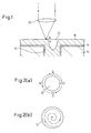
- a thick metallic layer 110 is formed on all surfaces of the core substrate 100, including an inner wall surface of a through-hole 106 bored in the core substrate 100 by a drill or others, by electrolytic plating in which a metallic layer 108 formed by electrolytic plating is used as a power supply layer (see Figs. 7(a) and 7(b)).
- the wiring patterns 102, 102, ... of a desired shape are formed by patterning a multi-metallic layer consisting of the metallic layer 108, the thin metallic layer 110a and the metallic layer 114 (see Fig. 7(g)) to result in the core substrate 100 shown in Fig. 6.
Landscapes
- Engineering & Computer Science (AREA)
- Manufacturing & Machinery (AREA)
- Microelectronics & Electronic Packaging (AREA)
- Printing Elements For Providing Electric Connections Between Printed Circuits (AREA)
- Production Of Multi-Layered Print Wiring Board (AREA)
- Manufacturing Of Printed Wiring (AREA)
Applications Claiming Priority (2)
| Application Number | Priority Date | Filing Date | Title |
|---|---|---|---|
| JP2003299706 | 2003-08-25 | ||
| JP2003299706A JP4280583B2 (ja) | 2003-08-25 | 2003-08-25 | ヴィアの形成方法 |
Publications (3)
| Publication Number | Publication Date |
|---|---|
| EP1511367A2 true EP1511367A2 (fr) | 2005-03-02 |
| EP1511367A3 EP1511367A3 (fr) | 2005-12-21 |
| EP1511367B1 EP1511367B1 (fr) | 2011-07-06 |
Family
ID=34101150
Family Applications (1)
| Application Number | Title | Priority Date | Filing Date |
|---|---|---|---|
| EP04254904A Expired - Lifetime EP1511367B1 (fr) | 2003-08-25 | 2004-08-16 | Fabrication d'un panneau à circuit |
Country Status (6)
| Country | Link |
|---|---|
| US (1) | US7205230B2 (fr) |
| EP (1) | EP1511367B1 (fr) |
| JP (1) | JP4280583B2 (fr) |
| KR (1) | KR20050022324A (fr) |
| CN (1) | CN100505989C (fr) |
| TW (1) | TW200513159A (fr) |
Cited By (1)
| Publication number | Priority date | Publication date | Assignee | Title |
|---|---|---|---|---|
| CN115484746A (zh) * | 2021-05-31 | 2022-12-16 | 宏启胜精密电子(秦皇岛)有限公司 | 电路板及其制造方法 |
Families Citing this family (19)
| Publication number | Priority date | Publication date | Assignee | Title |
|---|---|---|---|---|
| JP4516320B2 (ja) * | 2004-01-08 | 2010-08-04 | シチズン電子株式会社 | Led基板 |
| US8308053B2 (en) | 2005-08-31 | 2012-11-13 | Micron Technology, Inc. | Microfeature workpieces having alloyed conductive structures, and associated methods |
| KR100753423B1 (ko) * | 2006-06-30 | 2007-08-30 | 주식회사 하이닉스반도체 | 비아패턴 형성방법 |
| KR100968977B1 (ko) * | 2008-10-17 | 2010-07-14 | 삼성전기주식회사 | 무수축 세라믹 기판 및 무수축 세라믹 기판의 제조 방법 |
| WO2011062037A1 (fr) * | 2009-11-20 | 2011-05-26 | イビデン株式会社 | Carte à circuit imprimé et son procédé de fabrication |
| CN102215641B (zh) * | 2011-05-04 | 2012-11-07 | 深圳市博敏电子有限公司 | 一种带盘中孔的高密度印制板的加工工艺 |
| JP2015029027A (ja) * | 2013-07-31 | 2015-02-12 | イビデン株式会社 | プリント配線板 |
| US9053972B1 (en) | 2013-11-21 | 2015-06-09 | Freescale Semiconductor, Inc. | Pillar bump formed using spot-laser |
| US9474162B2 (en) | 2014-01-10 | 2016-10-18 | Freescale Semiocnductor, Inc. | Circuit substrate and method of manufacturing same |
| JP7009362B2 (ja) * | 2015-10-30 | 2022-01-25 | シューラット テクノロジーズ,インク. | 付加製造システム及び方法 |
| US10478311B2 (en) | 2017-08-14 | 2019-11-19 | Globus Medical, Inc. | Medical devices including titanium surface treatment |
| CN109673112B (zh) * | 2017-10-13 | 2021-08-20 | 鹏鼎控股(深圳)股份有限公司 | 柔性电路板以及柔性电路板的制作方法 |
| US10212828B1 (en) | 2017-11-27 | 2019-02-19 | International Business Machines Corporation | Via stub elimination by disrupting plating |
| JP7063095B2 (ja) * | 2018-05-07 | 2022-05-09 | 住友電気工業株式会社 | プリント配線板及びプリント配線板の製造方法 |
| US20190357364A1 (en) * | 2018-05-17 | 2019-11-21 | At&S Austria Technologie & Systemtechnik Aktiengesellschaft | Component Carrier With Only Partially Filled Thermal Through-Hole |
| KR102799625B1 (ko) | 2018-11-16 | 2025-04-23 | 삼성디스플레이 주식회사 | 표시 장치 및 이의 제조 방법 |
| CN110545620A (zh) * | 2019-08-06 | 2019-12-06 | 宁波华远电子科技有限公司 | 一种线路板通孔的填孔工艺 |
| WO2021049624A1 (fr) * | 2019-09-13 | 2021-03-18 | 株式会社ゼファー | Composant de circuit moulé et dispositif électronique |
| US12162074B2 (en) | 2020-11-25 | 2024-12-10 | Lawrence Livermore National Security, Llc | System and method for large-area pulsed laser melting of metallic powder in a laser powder bed fusion application |
Family Cites Families (13)
| Publication number | Priority date | Publication date | Assignee | Title |
|---|---|---|---|---|
| US4920070A (en) * | 1987-02-19 | 1990-04-24 | Fujitsu Limited | Method for forming wirings for a semiconductor device by filling very narrow via holes |
| US5110759A (en) * | 1988-12-20 | 1992-05-05 | Fujitsu Limited | Conductive plug forming method using laser planarization |
| JPH0350888A (ja) | 1989-07-19 | 1991-03-05 | Fujitsu Ltd | 導体ビアの修復方法 |
| US5380678A (en) * | 1991-03-12 | 1995-01-10 | Yu; Chang | Bilayer barrier metal method for obtaining 100% step-coverage in contact vias without junction degradation |
| US5340947A (en) | 1992-06-22 | 1994-08-23 | Cirqon Technologies Corporation | Ceramic substrates with highly conductive metal vias |
| US5454928A (en) | 1994-01-14 | 1995-10-03 | Watkins Johnson Company | Process for forming solid conductive vias in substrates |
| WO2001091924A1 (fr) * | 2000-06-01 | 2001-12-06 | Board Of Regents, The University Of Texas System | Frittage laser direct selectif de metaux |
| JP2002016357A (ja) | 2000-06-30 | 2002-01-18 | Shinko Electric Ind Co Ltd | 多層配線基板の製造方法及び半導体装置 |
| JP4582938B2 (ja) | 2001-02-28 | 2010-11-17 | 京セラ株式会社 | 絶縁シートの製造方法および配線基板の製造方法 |
| JP2002270718A (ja) * | 2001-03-07 | 2002-09-20 | Seiko Epson Corp | 配線基板及びその製造方法、半導体装置及びその製造方法、回路基板並びに電子機器 |
| US6504111B2 (en) | 2001-05-29 | 2003-01-07 | International Business Machines Corporation | Solid via layer to layer interconnect |
| JP3807312B2 (ja) | 2002-01-18 | 2006-08-09 | 富士通株式会社 | プリント基板とその製造方法 |
| US6835657B2 (en) * | 2002-12-02 | 2004-12-28 | Applied Materials, Inc. | Method for recrystallizing metal in features of a semiconductor chip |
-
2003
- 2003-08-25 JP JP2003299706A patent/JP4280583B2/ja not_active Expired - Fee Related
-
2004
- 2004-08-10 US US10/914,227 patent/US7205230B2/en not_active Expired - Fee Related
- 2004-08-11 TW TW093124033A patent/TW200513159A/zh unknown
- 2004-08-16 EP EP04254904A patent/EP1511367B1/fr not_active Expired - Lifetime
- 2004-08-20 KR KR1020040065730A patent/KR20050022324A/ko not_active Withdrawn
- 2004-08-24 CN CNB200410056988XA patent/CN100505989C/zh not_active Expired - Fee Related
Non-Patent Citations (1)
| Title |
|---|
| None |
Cited By (1)
| Publication number | Priority date | Publication date | Assignee | Title |
|---|---|---|---|---|
| CN115484746A (zh) * | 2021-05-31 | 2022-12-16 | 宏启胜精密电子(秦皇岛)有限公司 | 电路板及其制造方法 |
Also Published As
| Publication number | Publication date |
|---|---|
| EP1511367B1 (fr) | 2011-07-06 |
| TW200513159A (en) | 2005-04-01 |
| US7205230B2 (en) | 2007-04-17 |
| US20050048770A1 (en) | 2005-03-03 |
| EP1511367A3 (fr) | 2005-12-21 |
| JP4280583B2 (ja) | 2009-06-17 |
| KR20050022324A (ko) | 2005-03-07 |
| CN100505989C (zh) | 2009-06-24 |
| CN1592553A (zh) | 2005-03-09 |
| JP2005072235A (ja) | 2005-03-17 |
Similar Documents
| Publication | Publication Date | Title |
|---|---|---|
| EP1511367B1 (fr) | Fabrication d'un panneau à circuit | |
| JP3629375B2 (ja) | 多層回路基板の製造方法 | |
| US7606038B2 (en) | Method for producing a printed circuit board with a heat radiating structure and a printed circuit board with a heat radiating structure | |
| KR100213857B1 (ko) | 반도체장치의 제조방법 및 반도체장치의 패키지 | |
| KR100751984B1 (ko) | 전자 부품의 제조 방법 및 전자 부품 | |
| JP2014232862A (ja) | 印刷回路基板 | |
| US20080277152A1 (en) | Printed Circuit Board and Its Designing Method, and Designing Method of Ic Package Terminal and Its Connecting Method | |
| US6730859B2 (en) | Substrate for mounting electronic parts thereon and method of manufacturing same | |
| JP2001053188A (ja) | 多層配線基板の製造方法 | |
| KR101355732B1 (ko) | 배선기판 제조방법 | |
| JP6743287B2 (ja) | 配線基板及びその製造方法 | |
| US7883614B2 (en) | Method of manufacturing electronic part and electronic part | |
| JP2004241771A (ja) | 電子パッケージ修正プロセス | |
| JP2006100789A (ja) | 電気配線構造の製作方法 | |
| JP3838800B2 (ja) | 多層プリント配線板製造方法 | |
| US7371682B2 (en) | Production method for electronic component and electronic component | |
| JP3583279B2 (ja) | 穴あけ加工方法 | |
| JP2000200975A (ja) | 多層配線基板の製造方法 | |
| CN100455162C (zh) | 电路板的制造方法 | |
| EP1494516A2 (fr) | Panneau à circuit et son procédé de fabrication | |
| CN111199948A (zh) | 封装基板及其制造方法 | |
| EP1014436A2 (fr) | Methode de fabrication d'une substrate | |
| JP2000299563A (ja) | プリント配線板におけるビアホール形成方法 | |
| JPH11509991A (ja) | 恒久的接続のために電気回路の上に隆起した金属接点を作成する方法 | |
| JP2004055633A (ja) | 配線基板の製造方法 |
Legal Events
| Date | Code | Title | Description |
|---|---|---|---|
| PUAI | Public reference made under article 153(3) epc to a published international application that has entered the european phase |
Free format text: ORIGINAL CODE: 0009012 |
|
| AK | Designated contracting states |
Kind code of ref document: A2 Designated state(s): AT BE BG CH CY CZ DE DK EE ES FI FR GB GR HU IE IT LI LU MC NL PL PT RO SE SI SK TR |
|
| AX | Request for extension of the european patent |
Extension state: AL HR LT LV MK |
|
| PUAL | Search report despatched |
Free format text: ORIGINAL CODE: 0009013 |
|
| AK | Designated contracting states |
Kind code of ref document: A3 Designated state(s): AT BE BG CH CY CZ DE DK EE ES FI FR GB GR HU IE IT LI LU MC NL PL PT RO SE SI SK TR |
|
| AX | Request for extension of the european patent |
Extension state: AL HR LT LV MK |
|
| 17P | Request for examination filed |
Effective date: 20060324 |
|
| AKX | Designation fees paid |
Designated state(s): DE FR GB |
|
| 17Q | First examination report despatched |
Effective date: 20100323 |
|
| GRAP | Despatch of communication of intention to grant a patent |
Free format text: ORIGINAL CODE: EPIDOSNIGR1 |
|
| GRAS | Grant fee paid |
Free format text: ORIGINAL CODE: EPIDOSNIGR3 |
|
| GRAA | (expected) grant |
Free format text: ORIGINAL CODE: 0009210 |
|
| AK | Designated contracting states |
Kind code of ref document: B1 Designated state(s): DE FR GB |
|
| REG | Reference to a national code |
Ref country code: GB Ref legal event code: FG4D |
|
| REG | Reference to a national code |
Ref country code: DE Ref legal event code: R096 Ref document number: 602004033352 Country of ref document: DE Effective date: 20110901 |
|
| PLBE | No opposition filed within time limit |
Free format text: ORIGINAL CODE: 0009261 |
|
| STAA | Information on the status of an ep patent application or granted ep patent |
Free format text: STATUS: NO OPPOSITION FILED WITHIN TIME LIMIT |
|
| 26N | No opposition filed |
Effective date: 20120411 |
|
| REG | Reference to a national code |
Ref country code: DE Ref legal event code: R097 Ref document number: 602004033352 Country of ref document: DE Effective date: 20120411 |
|
| PGFP | Annual fee paid to national office [announced via postgrant information from national office to epo] |
Ref country code: DE Payment date: 20130814 Year of fee payment: 10 |
|
| PGFP | Annual fee paid to national office [announced via postgrant information from national office to epo] |
Ref country code: GB Payment date: 20130814 Year of fee payment: 10 Ref country code: FR Payment date: 20130808 Year of fee payment: 10 |
|
| REG | Reference to a national code |
Ref country code: DE Ref legal event code: R119 Ref document number: 602004033352 Country of ref document: DE |
|
| GBPC | Gb: european patent ceased through non-payment of renewal fee |
Effective date: 20140816 |
|
| REG | Reference to a national code |
Ref country code: DE Ref legal event code: R119 Ref document number: 602004033352 Country of ref document: DE Effective date: 20150303 |
|
| REG | Reference to a national code |
Ref country code: FR Ref legal event code: ST Effective date: 20150430 |
|
| PG25 | Lapsed in a contracting state [announced via postgrant information from national office to epo] |
Ref country code: GB Free format text: LAPSE BECAUSE OF NON-PAYMENT OF DUE FEES Effective date: 20140816 Ref country code: DE Free format text: LAPSE BECAUSE OF NON-PAYMENT OF DUE FEES Effective date: 20150303 |
|
| PG25 | Lapsed in a contracting state [announced via postgrant information from national office to epo] |
Ref country code: FR Free format text: LAPSE BECAUSE OF NON-PAYMENT OF DUE FEES Effective date: 20140901 |