EP1511367A2 - Manufacturing a wiring board - Google Patents
Manufacturing a wiring board Download PDFInfo
- Publication number
- EP1511367A2 EP1511367A2 EP04254904A EP04254904A EP1511367A2 EP 1511367 A2 EP1511367 A2 EP 1511367A2 EP 04254904 A EP04254904 A EP 04254904A EP 04254904 A EP04254904 A EP 04254904A EP 1511367 A2 EP1511367 A2 EP 1511367A2
- Authority
- EP
- European Patent Office
- Prior art keywords
- metal
- substrate
- hole
- laser beam
- less portion
- Prior art date
- Legal status (The legal status is an assumption and is not a legal conclusion. Google has not performed a legal analysis and makes no representation as to the accuracy of the status listed.)
- Granted
Links
Images


Classifications
-
- H—ELECTRICITY
- H05—ELECTRIC TECHNIQUES NOT OTHERWISE PROVIDED FOR
- H05K—PRINTED CIRCUITS; CASINGS OR CONSTRUCTIONAL DETAILS OF ELECTRIC APPARATUS; MANUFACTURE OF ASSEMBLAGES OF ELECTRICAL COMPONENTS
- H05K3/00—Apparatus or processes for manufacturing printed circuits
- H05K3/22—Secondary treatment of printed circuits
-
- H—ELECTRICITY
- H05—ELECTRIC TECHNIQUES NOT OTHERWISE PROVIDED FOR
- H05K—PRINTED CIRCUITS; CASINGS OR CONSTRUCTIONAL DETAILS OF ELECTRIC APPARATUS; MANUFACTURE OF ASSEMBLAGES OF ELECTRICAL COMPONENTS
- H05K3/00—Apparatus or processes for manufacturing printed circuits
- H05K3/40—Forming printed elements for providing electric connections to or between printed circuits
- H05K3/42—Plated through-holes or plated via connections
- H05K3/423—Plated through-holes or plated via connections characterised by electroplating method
-
- H—ELECTRICITY
- H05—ELECTRIC TECHNIQUES NOT OTHERWISE PROVIDED FOR
- H05K—PRINTED CIRCUITS; CASINGS OR CONSTRUCTIONAL DETAILS OF ELECTRIC APPARATUS; MANUFACTURE OF ASSEMBLAGES OF ELECTRICAL COMPONENTS
- H05K3/00—Apparatus or processes for manufacturing printed circuits
- H05K3/46—Manufacturing multilayer circuits
-
- H—ELECTRICITY
- H01—ELECTRIC ELEMENTS
- H01L—SEMICONDUCTOR DEVICES NOT COVERED BY CLASS H10
- H01L2924/00—Indexing scheme for arrangements or methods for connecting or disconnecting semiconductor or solid-state bodies as covered by H01L24/00
- H01L2924/0001—Technical content checked by a classifier
- H01L2924/0002—Not covered by any one of groups H01L24/00, H01L24/00 and H01L2224/00
-
- H—ELECTRICITY
- H05—ELECTRIC TECHNIQUES NOT OTHERWISE PROVIDED FOR
- H05K—PRINTED CIRCUITS; CASINGS OR CONSTRUCTIONAL DETAILS OF ELECTRIC APPARATUS; MANUFACTURE OF ASSEMBLAGES OF ELECTRICAL COMPONENTS
- H05K2201/00—Indexing scheme relating to printed circuits covered by H05K1/00
- H05K2201/09—Shape and layout
- H05K2201/09209—Shape and layout details of conductors
- H05K2201/095—Conductive through-holes or vias
- H05K2201/09536—Buried plated through-holes, i.e. plated through-holes formed in a core before lamination
-
- H—ELECTRICITY
- H05—ELECTRIC TECHNIQUES NOT OTHERWISE PROVIDED FOR
- H05K—PRINTED CIRCUITS; CASINGS OR CONSTRUCTIONAL DETAILS OF ELECTRIC APPARATUS; MANUFACTURE OF ASSEMBLAGES OF ELECTRICAL COMPONENTS
- H05K2201/00—Indexing scheme relating to printed circuits covered by H05K1/00
- H05K2201/09—Shape and layout
- H05K2201/09209—Shape and layout details of conductors
- H05K2201/095—Conductive through-holes or vias
- H05K2201/09563—Metal filled via
-
- H—ELECTRICITY
- H05—ELECTRIC TECHNIQUES NOT OTHERWISE PROVIDED FOR
- H05K—PRINTED CIRCUITS; CASINGS OR CONSTRUCTIONAL DETAILS OF ELECTRIC APPARATUS; MANUFACTURE OF ASSEMBLAGES OF ELECTRICAL COMPONENTS
- H05K2201/00—Indexing scheme relating to printed circuits covered by H05K1/00
- H05K2201/09—Shape and layout
- H05K2201/09209—Shape and layout details of conductors
- H05K2201/095—Conductive through-holes or vias
- H05K2201/096—Vertically aligned vias, holes or stacked vias
-
- H—ELECTRICITY
- H05—ELECTRIC TECHNIQUES NOT OTHERWISE PROVIDED FOR
- H05K—PRINTED CIRCUITS; CASINGS OR CONSTRUCTIONAL DETAILS OF ELECTRIC APPARATUS; MANUFACTURE OF ASSEMBLAGES OF ELECTRICAL COMPONENTS
- H05K2201/00—Indexing scheme relating to printed circuits covered by H05K1/00
- H05K2201/09—Shape and layout
- H05K2201/09209—Shape and layout details of conductors
- H05K2201/09654—Shape and layout details of conductors covering at least two types of conductors provided for in H05K2201/09218 - H05K2201/095
- H05K2201/09745—Recess in conductor, e.g. in pad or in metallic substrate
-
- H—ELECTRICITY
- H05—ELECTRIC TECHNIQUES NOT OTHERWISE PROVIDED FOR
- H05K—PRINTED CIRCUITS; CASINGS OR CONSTRUCTIONAL DETAILS OF ELECTRIC APPARATUS; MANUFACTURE OF ASSEMBLAGES OF ELECTRICAL COMPONENTS
- H05K2201/00—Indexing scheme relating to printed circuits covered by H05K1/00
- H05K2201/10—Details of components or other objects attached to or integrated in a printed circuit board
- H05K2201/10227—Other objects, e.g. metallic pieces
- H05K2201/1025—Metallic discs
-
- H—ELECTRICITY
- H05—ELECTRIC TECHNIQUES NOT OTHERWISE PROVIDED FOR
- H05K—PRINTED CIRCUITS; CASINGS OR CONSTRUCTIONAL DETAILS OF ELECTRIC APPARATUS; MANUFACTURE OF ASSEMBLAGES OF ELECTRICAL COMPONENTS
- H05K2203/00—Indexing scheme relating to apparatus or processes for manufacturing printed circuits covered by H05K3/00
- H05K2203/10—Using electric, magnetic and electromagnetic fields; Using laser light
- H05K2203/107—Using laser light
-
- H—ELECTRICITY
- H05—ELECTRIC TECHNIQUES NOT OTHERWISE PROVIDED FOR
- H05K—PRINTED CIRCUITS; CASINGS OR CONSTRUCTIONAL DETAILS OF ELECTRIC APPARATUS; MANUFACTURE OF ASSEMBLAGES OF ELECTRICAL COMPONENTS
- H05K2203/00—Indexing scheme relating to apparatus or processes for manufacturing printed circuits covered by H05K3/00
- H05K2203/12—Using specific substances
- H05K2203/128—Molten metals, e.g. casting thereof, or melting by heating and excluding molten solder
-
- H—ELECTRICITY
- H05—ELECTRIC TECHNIQUES NOT OTHERWISE PROVIDED FOR
- H05K—PRINTED CIRCUITS; CASINGS OR CONSTRUCTIONAL DETAILS OF ELECTRIC APPARATUS; MANUFACTURE OF ASSEMBLAGES OF ELECTRICAL COMPONENTS
- H05K3/00—Apparatus or processes for manufacturing printed circuits
- H05K3/10—Apparatus or processes for manufacturing printed circuits in which conductive material is applied to the insulating support in such a manner as to form the desired conductive pattern
- H05K3/102—Apparatus or processes for manufacturing printed circuits in which conductive material is applied to the insulating support in such a manner as to form the desired conductive pattern by bonding of conductive powder, i.e. metallic powder
-
- H—ELECTRICITY
- H05—ELECTRIC TECHNIQUES NOT OTHERWISE PROVIDED FOR
- H05K—PRINTED CIRCUITS; CASINGS OR CONSTRUCTIONAL DETAILS OF ELECTRIC APPARATUS; MANUFACTURE OF ASSEMBLAGES OF ELECTRICAL COMPONENTS
- H05K3/00—Apparatus or processes for manufacturing printed circuits
- H05K3/46—Manufacturing multilayer circuits
- H05K3/4602—Manufacturing multilayer circuits characterized by a special circuit board as base or central core whereon additional circuit layers are built or additional circuit boards are laminated
Definitions
- a thick metallic layer 110 is formed on all surfaces of the core substrate 100, including an inner wall surface of a through-hole 106 bored in the core substrate 100 by a drill or others, by electrolytic plating in which a metallic layer 108 formed by electrolytic plating is used as a power supply layer (see Figs. 7(a) and 7(b)).
- the wiring patterns 102, 102, ... of a desired shape are formed by patterning a multi-metallic layer consisting of the metallic layer 108, the thin metallic layer 110a and the metallic layer 114 (see Fig. 7(g)) to result in the core substrate 100 shown in Fig. 6.
Landscapes
- Engineering & Computer Science (AREA)
- Manufacturing & Machinery (AREA)
- Microelectronics & Electronic Packaging (AREA)
- Printing Elements For Providing Electric Connections Between Printed Circuits (AREA)
- Production Of Multi-Layered Print Wiring Board (AREA)
- Manufacturing Of Printed Wiring (AREA)
Abstract
Description
- The present invention relates to a process for manufacturing a wiring board having a via and, more specifically, to a method for forming a via penetrating a substrate made of an insulation material while filling metal, by plating in a through-hole formed in the substrate, so that a plated metallic layer of a predetermined thickness is formed on the surface of the substrate.
- A multi-layer wiring substrate shown in Fig. 6 is used in an electronic part such as a semiconductor device. In the multi-layer wiring substrate shown in Fig. 6,
wiring patterns core substrate 100 of an insulation material such as a ceramic, a resin or others, are electrically connected towiring patterns insulation layers vias core substrate 100 andvias insulation layers - A method for manufacturing such a
core substrate 100 is disclosed, for example, in Japanese Unexamined Patent Publication (Kokai) No. 2002-16357 (paragraphs [0034] to [0047], Figs. 2 and 3). - The method for manufacturing the
core substrate 100 described in the above-mentioned patent document will be explained below with reference to Figs. 7(a) to 7(g). - First, a thick
metallic layer 110 is formed on all surfaces of thecore substrate 100, including an inner wall surface of a through-hole 106 bored in thecore substrate 100 by a drill or others, by electrolytic plating in which ametallic layer 108 formed by electrolytic plating is used as a power supply layer (see Figs. 7(a) and 7(b)). - Further, the through-
hole 106, in which themetallic layers resin 112, so that dome-like portions 112a are formed at opposite openings of the through-hole 106 (see Fig. 7(c)). Then, themetallic layer 110 is subjected to the etching while using the dome-like portion 112a as a mask and is thinned to be a thinmetallic layer 110a (see Fig. 7(d)). - Then, the dome-
like portion 112a is removed by the grinding or others so that an exposed surface of theresin 112 is flush with the surface of the thinmetallic layer 110a (see Fig. 7(e)), and thereafter, ametallic layer 114 is formed on the thinmetallic layer 110a and the exposed surface of theresin layer 112 by the electroless plating, whereby thevia 104 penetrating thecore substrate 100 is obtained (Fig. 7(f)). - Thereafter, the
wiring patterns metallic layer 108, the thinmetallic layer 110a and the metallic layer 114 (see Fig. 7(g)) to result in thecore substrate 100 shown in Fig. 6. - According to the
core substrate 100 shown in Figs. 6 and 7(a) to 7(g), thewiring patterns 102 are formed on opposite ends of thevias wiring pattern 102. - However, as the
via 104 of thecore substrate 100 is formed of metal and resin, the electric properties thereof being largely different from each other, an improvement in electrical characteristics, such as impedance, is limited. - In this regard, it has been proposed to fill metal, by plating, in a through-hole, in advance, during the formation of a substrate made of an insulation material.
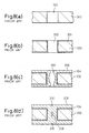
- According to this method for forming the via, after forming a through-
hole 202 in asubstrate 200 made of an insulation material, as shown in Fig. 8(a), aseed layer 204 of metal is formed on a surface of thesubstrate 200 including an inner wall surface of the through-hole 202 by electroless plating as shown in Fig. 8(b). - Then, electrolytic plating is carried out while using the
seed layer 204 as a power supply layer, to form a platedmetallic layer 206 on theseed layer 204 as shown in Fig. 8(c). - When the electrolytic plating is continued, the through-
hole 202 is filled with metal to complete the via as shown in Fig. 8(d), and the platedmetallic layer 206 of a predetermined thickness is formed on the surface of thesubstrate 200. - Thereafter, the plated
metallic layer 206 is patterned to form a desired wiring pattern on each of the opposite surfaces of thesubstrate 200. Thus, a wiring substrate having the via, both of which ends are connected to the wiring patterns, is obtained. - However, as shown in Fig. 8(d), a
void 208 may possibly be generated in the via ordimples metallic layer 206 at positions corresponding to the center of the openings of the through-hole 202. - If the depth of
such dimples metallic layers 206 formed on the respective surfaces of thesubstrate 200, it is possible to remove thedimples metallic layer 206 by etching or other methods. - However, if the depth of the
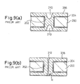
dimples metallic layer 206 as shown in Fig. 9(a), thedimples metallic layer 206 is removed by etching or other methods. - Also, if the through-
hole 202 is not completely closed to leave a thin hole (seam) 212 as shown in Fig. 9(b), theseam 212 is still left as it is even if the platedmetallic layer 202 is removed by the etching or others. - In addition, a number of vias must be formed, in general, in the
core substrate 100, and it is extremely difficult to optimize the plating condition for all the through-holes 202 formed in thesubstrate 200. Accordingly, there may be some vias having thedimple 210 or theseam 212 among the plurality of vias formed in thesubstrate 200. - There is a risk, in the substrate having vias in which dimples 210 or
seams 212 exist, that the electric connection between the via and the wiring pattern becomes worse if the wiring pattern is formed directly on each of the opposite end surfaces of the respective via. Accordingly, in general, a wiring pad having a diameter larger than that of the through-hole 202 is provided on each of the opposite end surfaces of the via to ensure the electric connection between the both. - However, the provision of the wiring pad having the larger diameter on each of the opposite end surfaces of the respective via is problematic in that the degree of freedom is reduced in the design of wiring pattern formed in the substrate, and a high-density arrangement of the wiring pattern becomes difficult.
- Accordingly, an object of the present invention is to provide a process for manufacturing a wiring board, having a via, particularly obtained by filling metal by plating in a through-hole formed in a substrate of insulation material, which via is non-problematic even if a wiring pattern is formed directly on the end surface thereof.
- The inventor of the present invention has attained the object on the basis of an idea that, when the via is formed by filling metal by plating in the through-hole formed in the substrate made of an insulation material, it is effective to fill metal in a metal-less portion of a plated metallic layer corresponding to the opening of the through-hole, such as a dimple or a seam, in which no metal is filled.
- By this study, the inventor has become aware of that it is possible to fill the metal-less portion with molten metal obtained by emitting a YAG laser beam to a plurality of points in the plated metallic layer in the vicinity of the peripheral edge of the opening having the metal-less portion, and has reached the present invention.
- According to the present invention, there is provided a process for manufacturing a wiring board comprising a substrate made of an insulation material and having first and second surfaces, first and second conductor patterns formed on the first and second surfaces, respectively, and a via conductor penetrating the substrate to electrically connect the first conductor pattern with the second conductor pattern; the process comprising the following steps of: forming the substrate with a through-hole penetrating thereto and defining openings at the first and second surfaces, respectively; plating the substrate with a metal so that a metal layer having a predetermined thickness is formed on the respective first and second surfaces of the substrate and the through-hole is substantially filled with the metal to be the via; irradiating a laser beam, as a plurality of spots, around a metal-vacant portion of the plated metal, such as a dimple or seam, at positions corresponding to the openings of the through-hole, so that a part of the plated metal melts to fill the metal-vacant portion with the molten metal.
- According to another aspect of the present invention, there is provided a process for manufacturing a wiring board comprising a substrate made of an insulation material and having first and second surfaces, first and second conductor patterns formed on the first and second surfaces, respectively, and a via conductor penetrating the substrate to electrically connect the first conductor pattern with the second conductor pattern; the process comprising the following steps of: forming the substrate with a through-hole to penetrate the substrate from the first surface to the second surface; plating the substrate with a metal so that a metal layer having a predetermined thickness is formed on the respective first and second surfaces of the substrate and the through-hole is substantially filled with the metal to be the via; covering with a metal foil or metal powder a metal-less portion of the plated metal, such as a dimple or seam, at positions corresponding to the openings of the through-hole; irradiating a laser beam, as a plurality of spots, onto the metal foil or metal powder, so that at least a part of the metal foil or powder melts to fill the metal-less portion with molten metal.
- According to the present invention, the laser beam is sequentially emitted along the peripheral edge of the metal-less portion to melt part of the plated metal layer in the vicinity of the peripheral edge of the metal-less portion, which molten metal is filled in the metal-less portion such as a dimple or a seam, formed in the plated metallic layer corresponding to the opening of the through-hole.
- Also, by sequentially emitting the laser beam along a spiral path starting from the proximity of the peripheral edge of the opening of the through-hole and going inward of the opening, the metal-less portion once filled with the molten metal is molten again, whereby it is possible to homogenize the plated metallic layer corresponding to the opening of the through-hole.
- According to the present invention, even if the metal-vacant portion, such as a dimple or a seam, is formed in the plated metallic layer at a position corresponding to the opening of the through-hole formed in the substrate of insulation material, it is possible to fill the metal-less portion with molten metal which is part of the plated metal layer in the vicinity of the peripheral edge of the metal-less portion by the spot-like emission of the laser beam onto a plurality of points thereof.
- In such a manner, by filling the metal-less portion with molten metal and removing the plated metallic layer formed on the surface of the substrate, it is possible to obtain a via having a flat end surface, on which can be directly formed the wiring pattern.
- As a result, it is possible to increase the degree of freedom in the design of wiring pattern formed in the substrate, and thus to facilitate the high-density arrangement of the wiring pattern.
-
- Fig. 1 is a schematic illustration for explaining one embodiment of the inventive method;
- Figs. 2(a) and 2(b) illustrate the order of the spot-like emission of a laser beam shown in Fig. 1;
- Fig. 3 illustrates a state of an opening after the spot-like emission of the laser beam in the order shown in Fig. 2(b);
- Fig. 4 is a schematic illustration for explaining another embodiment of the inventive method;
- Fig. 5 is a schematic illustration for explaining a further embodiment of the inventive method;
- Fig. 6 is a sectional view for illustrating one example of a multi-layer wiring substrate;
- Figs. 7(a) to 7(g) illustrate a method for manufacturing a core substrate constituting the multi-layer wiring substrate shown in Fig. 6;
- Figs. 8(a) to 8(d) illustrate another method for manufacturing a core substrate constituting the multi-layer wiring substrate shown in Fig. 6; and
- Figs. 9(a) and 9(b) are partially sectional views for explaining the problems in the method for manufacturinq the core substrate shown in Fig. 8.
-
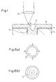
- As shown in Fig. 1, a through-
hole 12 formed in asubstrate 10 of insulation material such as resin is filled with metal such as copper by plating. The filling of the metal in the through-hole 12 by plating is carried out in the same manner as shown in Fig. 8. - That is, a
seed layer 14 consisting of metal such as copper is formed on the surface of thesubstrate 10 including the inner wall surface of the through-hole 12 formed in thesubstrate 10 of insulation material such as resin by electroless plating and, thereafter, a platedmetallic layer 16 having a predetermined thickness is formed on theseed layer 14 while filling the through-hole 12, with metal such as copper, by the electrolytic plating wherein theseed layer 14 is used as a power supply layer. - As shown in Fig. 1, there may be a dimple 20 which is a recess of a metal-less portion in the plated
metallic layer 16 at a position in correspondence to the opening of the through-hole 12. This dimple 20 is deep and would be left on an end surface of a via even if the platedmetallic layer 16 is removed by etching or other methods. - A YAG laser beam focused by a
lens 22 is emitted as a "spot" onto the platedmetallic layer 16 forming the proximity of the peripheral edge of the dimple 20 to melt part of the platedmetallic layer 16. The molten metal flows in the direction indicated by an arrow A to fill the dimple 20. - An amount of molten metal obtained by one "spot-like" emission is small. That is to say, the "spot-like" emission means a laser beam emission to be irradiated on to a very small area. Accordingly, it is necessary to repeat the "spot-like" emission of the YAG laser beam a plurality of times so that the
dimple 20 is sufficiently filled with molten metal. At that time, if the "spot-like" emission of the YAG laser beam is repeated at the same point, this point is deeply excavated. To avoid such a trouble, the "spot-like" emission of the YAG laser beam is carried out to a plurality of different points in the vicinity of the peripheral edge of thedimple 20. - When the YAG laser beam is emitted to four points a, b, c and d along the peripheral edge of the
dimple 20, for example, as shown in Fig. 2(a), the spot-like emission of the YAG laser beam is preferably carried out in the order of point a to point b, to point c, and to point d. - By repeating the "spot-like" emission of the YAG laser beam a plurality of times in such a manner, the
dimple 20 is filled with metal. A degree at which thedimple 20 is filled with metal is such that thedimple 20 is not necessarily completely filled with the metal but disappears after the platedmetallic layer 16 has been removed by the etching or others. - Also, the spot-like emission of the YAG laser beam may be sequentially carried out along a spiral path, for example, shown in Fig. 2(b), starting from the proximity of the peripheral edge of the opening of the through-
hole 12 and going inward of the opening, whereby a portion of thedimple 20 which has been once filled with the metal is molten again to homogenize the platedmetallic layer 16 in correspondence with the opening of the through-hole 12. Fig. 3 illustrates a state of the opening obtained by the spot-like emission of the YAG laser beam along the spiral path starting from the proximity of the peripheral edge of the opening of the through-hole 12 and going inward of the opening. A diameter of the opening of the through-hole 12 is 193µm and the number of the spot-like emission of the YAG laser beam is 579 times. - As described above, by the spot-like emission of the YAG laser beam sequentially carried out along the spiral path starting from the proximity of the peripheral edge of the opening of the through-
hole 12 and going inward of the opening, it is possible, of course, to fill thedimple 20 with metal, as well as to reduce or eliminate the void 208 shown in Fig. 8(d) due to the heating of all the metal filled in the through-hole 12. - After the
dimple 20 has been filled with metal by the "spot-like" emission of the YAG laser beam described above, the platedmetallic layer 16 is removed by the etching or others to result in the via, penetrating thesubstrate 10, having flat opposite end surfaces. - It is possible to form a wiring pattern directly on each of the opposite end surfaces of the via, without the necessity for providing a wiring pad having a diameter larger than that of the via. Thereby, the degree of freedom increases in the design of the wiring pattern formed in the
substrate 10, and a high-density arrangement of the wiring pattern can be realized. - While part of the plated
metallic layer 16 is molten by the repeated spot-like emission of the YAG laser beam to fill thedimple 20 with the molten metal in Figs. 1 to 3, there is a risk, in this case, that the dimple is not sufficiently filled with the molten metal if thedimple 20 has a large diameter. - To solve such a problem, as shown in Fig. 4, the
dimple 20 formed in the platedmetallic layer 16 at a position corresponding to the opening of the through-hole 12 is covered withmetallic powder 24 of the same kind as that forming the platedmetallic layer 16. - Then, the YAG laser beam is spot-likely emitted to a plurality of positions of the
metallic powder 24 to melt at least part of themetallic powder 24 and fill the same in thedimple 20. - By melting part of the
metallic powder 24 filled in thedimple 20 in advance by the spot-like emission of the YAG laser beam and fill thedimple 20 with the molten metal, it is possible to sufficiently fill thedimple 20 with the metal even if the dimple has a large diameter. - Thereafter, non-molten
metallic powder 24 is removed if necessary, and the platedmetallic layer 16 is removed by etching or other methods, whereby the via having a flat end surface is obtainable. - Alternatively, as shown in Fig. 5, after covering the
dimple 20 formed in the platedmetallic layer 16 at a position corresponding to the opening of the through-hole 12 withmetallic foil 26 of the same kind as that forming the platedmetallic layer 16, the YAG laser beam is emitted onto a plurality of portions of themetallic foil 26 to melt at least part thereof and fill thedimple 20 with the molten metal. - In this regard, while the YAG laser beam has been used as a laser beam in the description with reference to Figs. 1 to 5, an excimer laser beam may be used in place of the YAG laser beam, if it would be preferable to use a laser beam having a different wavelength.
- Further, while the method for filling the
dimple 20 formed in the platedmetallic layer 16 at a position corresponding to the opening of the through-hole 12 has been described with reference to Figs. 1 to 5, this method may be applied to the filling of theseam 212 shown in Fig. 9(b). - In a practical application of this invention, the emission of YAG laser is carried out automatically in accordance with a program regarding the design for the individual wiring board.
Claims (6)
- A process for manufacturing a wiring board comprising a substrate made of an insulation material and having first and second surfaces, first and second conductor patterns formed on the first and second surfaces, respectively, and a via conductor penetrating the substrate to electrically connect the first conductor pattern with the second conductor pattern; the process comprising the following steps of:forming the substrate with a through-hole penetrating thereto and defining openings at the first and second surfaces, respectively;plating the substrate with a metal so that a metal layer having a predetermined thickness is formed on the respective first and second surfaces of the substrate and the through-hole is substantially filled with the metal to be the via;emitting a laser beam, as a plurality of spots, around a metal-less portion of the plated metal, such as a dimple or seam, at positions corresponding to the openings of the through-hole, so that the a part of the plated metal melts to fill the metal-less portion with the molten metal.
- A process as set forth in claim 1, wherein the laser beam is irradiated periodically along a circular peripheral edge of a recess of the metal-less portion.
- A process as set forth in claim 1, wherein the laser beam is irradiated periodically along a spiral path inwardly from a peripheral edge of a recess of the metal-less portion.
- A process for manufacturing a wiring board comprising a substrate made of an insulation material and having first and second surfaces, first and second conductor patterns formed on the first and second surfaces, respectively, and a via conductor penetrating the substrate to electrically connect the first conductor pattern with the second conductor pattern; the process comprising the following steps of:forming the substrate with a through-hole to penetrate the substrate from the first surface to the second surface;plating the substrate with a metal so that a metal layer having a predetermined thickness is formed on the respective first and second surfaces of the substrate and the through-hole is substantially filled with the metal to be the via;covering with a metal foil or metal powder a metal-less portion of the plated metal, such as a dimple or seam, at positions corresponding to the openings of the through-hole;irradiating a laser beam, as a plurality of spots, onto the metal foil or metal powder, so that at least a part of the metal foil or powder melts to fill the metal-less portion with molten metal.
- A process as set forth in claim 4, wherein the laser beam is irradiated periodically along a circular peripheral edge of the metal-less portion.
- A process as set forth in claim 4, wherein the laser beam is irradiated periodically along a spiral path inwardly from a peripheral edge of the metal-less portion.
Applications Claiming Priority (2)
| Application Number | Priority Date | Filing Date | Title |
|---|---|---|---|
| JP2003299706A JP4280583B2 (en) | 2003-08-25 | 2003-08-25 | Via formation method |
| JP2003299706 | 2003-08-25 |
Publications (3)
| Publication Number | Publication Date |
|---|---|
| EP1511367A2 true EP1511367A2 (en) | 2005-03-02 |
| EP1511367A3 EP1511367A3 (en) | 2005-12-21 |
| EP1511367B1 EP1511367B1 (en) | 2011-07-06 |
Family
ID=34101150
Family Applications (1)
| Application Number | Title | Priority Date | Filing Date |
|---|---|---|---|
| EP04254904A Expired - Fee Related EP1511367B1 (en) | 2003-08-25 | 2004-08-16 | Manufacturing a wiring board |
Country Status (6)
| Country | Link |
|---|---|
| US (1) | US7205230B2 (en) |
| EP (1) | EP1511367B1 (en) |
| JP (1) | JP4280583B2 (en) |
| KR (1) | KR20050022324A (en) |
| CN (1) | CN100505989C (en) |
| TW (1) | TW200513159A (en) |
Families Citing this family (18)
| Publication number | Priority date | Publication date | Assignee | Title |
|---|---|---|---|---|
| JP4516320B2 (en) * | 2004-01-08 | 2010-08-04 | シチズン電子株式会社 | LED board |
| US8308053B2 (en) | 2005-08-31 | 2012-11-13 | Micron Technology, Inc. | Microfeature workpieces having alloyed conductive structures, and associated methods |
| KR100753423B1 (en) * | 2006-06-30 | 2007-08-30 | 주식회사 하이닉스반도체 | Method of forming via pattern |
| KR100968977B1 (en) * | 2008-10-17 | 2010-07-14 | 삼성전기주식회사 | Non-shiringkage ceramic substrate and manufacturing method thereof |
| WO2011062037A1 (en) * | 2009-11-20 | 2011-05-26 | イビデン株式会社 | Printed circuit board and manufacturing method of printed circuit board |
| CN102215641B (en) * | 2011-05-04 | 2012-11-07 | 深圳市博敏电子有限公司 | Manufacturing process of high-density printed board with holes in pads |
| JP2015029027A (en) * | 2013-07-31 | 2015-02-12 | イビデン株式会社 | Printed wiring board |
| US9053972B1 (en) | 2013-11-21 | 2015-06-09 | Freescale Semiconductor, Inc. | Pillar bump formed using spot-laser |
| US9474162B2 (en) | 2014-01-10 | 2016-10-18 | Freescale Semiocnductor, Inc. | Circuit substrate and method of manufacturing same |
| US10583484B2 (en) * | 2015-10-30 | 2020-03-10 | Seurat Technologies, Inc. | Multi-functional ingester system for additive manufacturing |
| US10478311B2 (en) | 2017-08-14 | 2019-11-19 | Globus Medical, Inc. | Medical devices including titanium surface treatment |
| CN109673112B (en) * | 2017-10-13 | 2021-08-20 | 鹏鼎控股(深圳)股份有限公司 | Flexible circuit board and manufacturing method thereof |
| US10212828B1 (en) * | 2017-11-27 | 2019-02-19 | International Business Machines Corporation | Via stub elimination by disrupting plating |
| JP7063095B2 (en) * | 2018-05-07 | 2022-05-09 | 住友電気工業株式会社 | Manufacturing method of printed wiring board and printed wiring board |
| US20190357364A1 (en) * | 2018-05-17 | 2019-11-21 | At&S Austria Technologie & Systemtechnik Aktiengesellschaft | Component Carrier With Only Partially Filled Thermal Through-Hole |
| KR20200057855A (en) | 2018-11-16 | 2020-05-27 | 삼성디스플레이 주식회사 | Display and manufacturing method of the same |
| CN110545620A (en) * | 2019-08-06 | 2019-12-06 | 宁波华远电子科技有限公司 | Hole filling process for through hole of circuit board |
| EP4029970A4 (en) * | 2019-09-13 | 2023-10-11 | Zefa Co., Ltd. | Molded circuit component and electronic device |
Family Cites Families (13)
| Publication number | Priority date | Publication date | Assignee | Title |
|---|---|---|---|---|
| US4920070A (en) * | 1987-02-19 | 1990-04-24 | Fujitsu Limited | Method for forming wirings for a semiconductor device by filling very narrow via holes |
| US5110759A (en) * | 1988-12-20 | 1992-05-05 | Fujitsu Limited | Conductive plug forming method using laser planarization |
| JPH0350888A (en) | 1989-07-19 | 1991-03-05 | Fujitsu Ltd | Restoration of conductor via |
| US5380678A (en) * | 1991-03-12 | 1995-01-10 | Yu; Chang | Bilayer barrier metal method for obtaining 100% step-coverage in contact vias without junction degradation |
| US5340947A (en) * | 1992-06-22 | 1994-08-23 | Cirqon Technologies Corporation | Ceramic substrates with highly conductive metal vias |
| US5454928A (en) * | 1994-01-14 | 1995-10-03 | Watkins Johnson Company | Process for forming solid conductive vias in substrates |
| EP1296776A4 (en) * | 2000-06-01 | 2004-12-08 | Univ Texas | Direct selective laser sintering of metals |
| JP2002016357A (en) | 2000-06-30 | 2002-01-18 | Shinko Electric Ind Co Ltd | Method of manufacturing multilayer wiring board and semiconductor device |
| JP4582938B2 (en) | 2001-02-28 | 2010-11-17 | 京セラ株式会社 | Insulating sheet manufacturing method and wiring board manufacturing method |
| JP2002270718A (en) * | 2001-03-07 | 2002-09-20 | Seiko Epson Corp | Wiring board and its manufacturing method, semiconductor device and its manufacturing method, and circuit board and electronic apparatus |
| US6504111B2 (en) * | 2001-05-29 | 2003-01-07 | International Business Machines Corporation | Solid via layer to layer interconnect |
| JP3807312B2 (en) * | 2002-01-18 | 2006-08-09 | 富士通株式会社 | Printed circuit board and manufacturing method thereof |
| US6835657B2 (en) * | 2002-12-02 | 2004-12-28 | Applied Materials, Inc. | Method for recrystallizing metal in features of a semiconductor chip |
-
2003
- 2003-08-25 JP JP2003299706A patent/JP4280583B2/en not_active Expired - Fee Related
-
2004
- 2004-08-10 US US10/914,227 patent/US7205230B2/en not_active Expired - Fee Related
- 2004-08-11 TW TW093124033A patent/TW200513159A/en unknown
- 2004-08-16 EP EP04254904A patent/EP1511367B1/en not_active Expired - Fee Related
- 2004-08-20 KR KR1020040065730A patent/KR20050022324A/en not_active Application Discontinuation
- 2004-08-24 CN CNB200410056988XA patent/CN100505989C/en not_active Expired - Fee Related
Non-Patent Citations (1)
| Title |
|---|
| None |
Also Published As
| Publication number | Publication date |
|---|---|
| CN1592553A (en) | 2005-03-09 |
| US20050048770A1 (en) | 2005-03-03 |
| JP4280583B2 (en) | 2009-06-17 |
| CN100505989C (en) | 2009-06-24 |
| KR20050022324A (en) | 2005-03-07 |
| EP1511367A3 (en) | 2005-12-21 |
| JP2005072235A (en) | 2005-03-17 |
| EP1511367B1 (en) | 2011-07-06 |
| TW200513159A (en) | 2005-04-01 |
| US7205230B2 (en) | 2007-04-17 |
Similar Documents
| Publication | Publication Date | Title |
|---|---|---|
| EP1511367B1 (en) | Manufacturing a wiring board | |
| JP3629375B2 (en) | Multilayer circuit board manufacturing method | |
| US7606038B2 (en) | Method for producing a printed circuit board with a heat radiating structure and a printed circuit board with a heat radiating structure | |
| KR100213857B1 (en) | Semiconductor device manufacturing method and package for semiconductor device | |
| US20080277152A1 (en) | Printed Circuit Board and Its Designing Method, and Designing Method of Ic Package Terminal and Its Connecting Method | |
| KR100751984B1 (en) | Process for producing electronic component and electronic component | |
| JP2006100789A (en) | Manufacturing method of electric wiring structure | |
| US6415504B1 (en) | Altering method of circuit pattern of printed-circuit board | |
| KR101355732B1 (en) | Wiring substrate manufacturing method | |
| JP2011222948A (en) | Method of manufacturing wiring board | |
| US6730859B2 (en) | Substrate for mounting electronic parts thereon and method of manufacturing same | |
| JP6743287B2 (en) | Wiring board and manufacturing method thereof | |
| US7883614B2 (en) | Method of manufacturing electronic part and electronic part | |
| JP2004241771A (en) | Electronic package correction process | |
| KR20050072678A (en) | Multilayer interconnection board and production method thereof | |
| JP3838800B2 (en) | Multilayer printed wiring board manufacturing method | |
| CN111199948A (en) | Package substrate and method for manufacturing the same | |
| US7371682B2 (en) | Production method for electronic component and electronic component | |
| JP3583279B2 (en) | Drilling method | |
| EP1494516A2 (en) | Wiring board and manufacturing method thereof | |
| EP1014436A2 (en) | Process for producing a substrate | |
| JP2000299563A (en) | Method for forming via hole in printed wiring board | |
| JP2020161730A (en) | Wiring board | |
| JPH11509991A (en) | Method of making raised metal contacts on electrical circuits for permanent connection | |
| JP2004055633A (en) | Method for manufacturing wiring board |
Legal Events
| Date | Code | Title | Description |
|---|---|---|---|
| PUAI | Public reference made under article 153(3) epc to a published international application that has entered the european phase |
Free format text: ORIGINAL CODE: 0009012 |
|
| AK | Designated contracting states |
Kind code of ref document: A2 Designated state(s): AT BE BG CH CY CZ DE DK EE ES FI FR GB GR HU IE IT LI LU MC NL PL PT RO SE SI SK TR |
|
| AX | Request for extension of the european patent |
Extension state: AL HR LT LV MK |
|
| PUAL | Search report despatched |
Free format text: ORIGINAL CODE: 0009013 |
|
| AK | Designated contracting states |
Kind code of ref document: A3 Designated state(s): AT BE BG CH CY CZ DE DK EE ES FI FR GB GR HU IE IT LI LU MC NL PL PT RO SE SI SK TR |
|
| AX | Request for extension of the european patent |
Extension state: AL HR LT LV MK |
|
| 17P | Request for examination filed |
Effective date: 20060324 |
|
| AKX | Designation fees paid |
Designated state(s): DE FR GB |
|
| 17Q | First examination report despatched |
Effective date: 20100323 |
|
| GRAP | Despatch of communication of intention to grant a patent |
Free format text: ORIGINAL CODE: EPIDOSNIGR1 |
|
| GRAS | Grant fee paid |
Free format text: ORIGINAL CODE: EPIDOSNIGR3 |
|
| GRAA | (expected) grant |
Free format text: ORIGINAL CODE: 0009210 |
|
| AK | Designated contracting states |
Kind code of ref document: B1 Designated state(s): DE FR GB |
|
| REG | Reference to a national code |
Ref country code: GB Ref legal event code: FG4D |
|
| REG | Reference to a national code |
Ref country code: DE Ref legal event code: R096 Ref document number: 602004033352 Country of ref document: DE Effective date: 20110901 |
|
| PLBE | No opposition filed within time limit |
Free format text: ORIGINAL CODE: 0009261 |
|
| STAA | Information on the status of an ep patent application or granted ep patent |
Free format text: STATUS: NO OPPOSITION FILED WITHIN TIME LIMIT |
|
| 26N | No opposition filed |
Effective date: 20120411 |
|
| REG | Reference to a national code |
Ref country code: DE Ref legal event code: R097 Ref document number: 602004033352 Country of ref document: DE Effective date: 20120411 |
|
| PGFP | Annual fee paid to national office [announced via postgrant information from national office to epo] |
Ref country code: DE Payment date: 20130814 Year of fee payment: 10 |
|
| PGFP | Annual fee paid to national office [announced via postgrant information from national office to epo] |
Ref country code: GB Payment date: 20130814 Year of fee payment: 10 Ref country code: FR Payment date: 20130808 Year of fee payment: 10 |
|
| REG | Reference to a national code |
Ref country code: DE Ref legal event code: R119 Ref document number: 602004033352 Country of ref document: DE |
|
| GBPC | Gb: european patent ceased through non-payment of renewal fee |
Effective date: 20140816 |
|
| REG | Reference to a national code |
Ref country code: DE Ref legal event code: R119 Ref document number: 602004033352 Country of ref document: DE Effective date: 20150303 |
|
| REG | Reference to a national code |
Ref country code: FR Ref legal event code: ST Effective date: 20150430 |
|
| PG25 | Lapsed in a contracting state [announced via postgrant information from national office to epo] |
Ref country code: GB Free format text: LAPSE BECAUSE OF NON-PAYMENT OF DUE FEES Effective date: 20140816 Ref country code: DE Free format text: LAPSE BECAUSE OF NON-PAYMENT OF DUE FEES Effective date: 20150303 |
|
| PG25 | Lapsed in a contracting state [announced via postgrant information from national office to epo] |
Ref country code: FR Free format text: LAPSE BECAUSE OF NON-PAYMENT OF DUE FEES Effective date: 20140901 |