EP1014436A2 - Methode de fabrication d'une substrate - Google Patents
Methode de fabrication d'une substrate Download PDFInfo
- Publication number
- EP1014436A2 EP1014436A2 EP99310230A EP99310230A EP1014436A2 EP 1014436 A2 EP1014436 A2 EP 1014436A2 EP 99310230 A EP99310230 A EP 99310230A EP 99310230 A EP99310230 A EP 99310230A EP 1014436 A2 EP1014436 A2 EP 1014436A2
- Authority
- EP
- European Patent Office
- Prior art keywords
- layer
- cavity
- masking layer
- conductor
- wall
- Prior art date
- Legal status (The legal status is an assumption and is not a legal conclusion. Google has not performed a legal analysis and makes no representation as to the accuracy of the status listed.)
- Withdrawn
Links
Images


Classifications
-
- H—ELECTRICITY
- H01—ELECTRIC ELEMENTS
- H01L—SEMICONDUCTOR DEVICES NOT COVERED BY CLASS H10
- H01L23/00—Details of semiconductor or other solid state devices
- H01L23/12—Mountings, e.g. non-detachable insulating substrates
-
- H—ELECTRICITY
- H01—ELECTRIC ELEMENTS
- H01L—SEMICONDUCTOR DEVICES NOT COVERED BY CLASS H10
- H01L21/00—Processes or apparatus adapted for the manufacture or treatment of semiconductor or solid state devices or of parts thereof
- H01L21/02—Manufacture or treatment of semiconductor devices or of parts thereof
- H01L21/04—Manufacture or treatment of semiconductor devices or of parts thereof the devices having at least one potential-jump barrier or surface barrier, e.g. PN junction, depletion layer or carrier concentration layer
- H01L21/48—Manufacture or treatment of parts, e.g. containers, prior to assembly of the devices, using processes not provided for in a single one of the subgroups H01L21/06 - H01L21/326
- H01L21/4814—Conductive parts
- H01L21/4846—Leads on or in insulating or insulated substrates, e.g. metallisation
- H01L21/486—Via connections through the substrate with or without pins
-
- H—ELECTRICITY
- H01—ELECTRIC ELEMENTS
- H01L—SEMICONDUCTOR DEVICES NOT COVERED BY CLASS H10
- H01L23/00—Details of semiconductor or other solid state devices
- H01L23/48—Arrangements for conducting electric current to or from the solid state body in operation, e.g. leads, terminal arrangements ; Selection of materials therefor
- H01L23/488—Arrangements for conducting electric current to or from the solid state body in operation, e.g. leads, terminal arrangements ; Selection of materials therefor consisting of soldered or bonded constructions
- H01L23/498—Leads, i.e. metallisations or lead-frames on insulating substrates, e.g. chip carriers
- H01L23/49805—Leads, i.e. metallisations or lead-frames on insulating substrates, e.g. chip carriers the leads being also applied on the sidewalls or the bottom of the substrate, e.g. leadless packages for surface mounting
-
- H—ELECTRICITY
- H05—ELECTRIC TECHNIQUES NOT OTHERWISE PROVIDED FOR
- H05K—PRINTED CIRCUITS; CASINGS OR CONSTRUCTIONAL DETAILS OF ELECTRIC APPARATUS; MANUFACTURE OF ASSEMBLAGES OF ELECTRICAL COMPONENTS
- H05K3/00—Apparatus or processes for manufacturing printed circuits
- H05K3/40—Forming printed elements for providing electric connections to or between printed circuits
- H05K3/403—Edge contacts; Windows or holes in the substrate having plural connections on the walls thereof
-
- H—ELECTRICITY
- H01—ELECTRIC ELEMENTS
- H01L—SEMICONDUCTOR DEVICES NOT COVERED BY CLASS H10
- H01L2224/00—Indexing scheme for arrangements for connecting or disconnecting semiconductor or solid-state bodies and methods related thereto as covered by H01L24/00
- H01L2224/01—Means for bonding being attached to, or being formed on, the surface to be connected, e.g. chip-to-package, die-attach, "first-level" interconnects; Manufacturing methods related thereto
- H01L2224/42—Wire connectors; Manufacturing methods related thereto
- H01L2224/47—Structure, shape, material or disposition of the wire connectors after the connecting process
- H01L2224/48—Structure, shape, material or disposition of the wire connectors after the connecting process of an individual wire connector
- H01L2224/4805—Shape
- H01L2224/4809—Loop shape
- H01L2224/48091—Arched
-
- H—ELECTRICITY
- H01—ELECTRIC ELEMENTS
- H01L—SEMICONDUCTOR DEVICES NOT COVERED BY CLASS H10
- H01L2224/00—Indexing scheme for arrangements for connecting or disconnecting semiconductor or solid-state bodies and methods related thereto as covered by H01L24/00
- H01L2224/01—Means for bonding being attached to, or being formed on, the surface to be connected, e.g. chip-to-package, die-attach, "first-level" interconnects; Manufacturing methods related thereto
- H01L2224/42—Wire connectors; Manufacturing methods related thereto
- H01L2224/47—Structure, shape, material or disposition of the wire connectors after the connecting process
- H01L2224/48—Structure, shape, material or disposition of the wire connectors after the connecting process of an individual wire connector
- H01L2224/481—Disposition
- H01L2224/48151—Connecting between a semiconductor or solid-state body and an item not being a semiconductor or solid-state body, e.g. chip-to-substrate, chip-to-passive
- H01L2224/48221—Connecting between a semiconductor or solid-state body and an item not being a semiconductor or solid-state body, e.g. chip-to-substrate, chip-to-passive the body and the item being stacked
- H01L2224/48225—Connecting between a semiconductor or solid-state body and an item not being a semiconductor or solid-state body, e.g. chip-to-substrate, chip-to-passive the body and the item being stacked the item being non-metallic, e.g. insulating substrate with or without metallisation
- H01L2224/48227—Connecting between a semiconductor or solid-state body and an item not being a semiconductor or solid-state body, e.g. chip-to-substrate, chip-to-passive the body and the item being stacked the item being non-metallic, e.g. insulating substrate with or without metallisation connecting the wire to a bond pad of the item
-
- H—ELECTRICITY
- H01—ELECTRIC ELEMENTS
- H01L—SEMICONDUCTOR DEVICES NOT COVERED BY CLASS H10
- H01L24/00—Arrangements for connecting or disconnecting semiconductor or solid-state bodies; Methods or apparatus related thereto
- H01L24/01—Means for bonding being attached to, or being formed on, the surface to be connected, e.g. chip-to-package, die-attach, "first-level" interconnects; Manufacturing methods related thereto
- H01L24/42—Wire connectors; Manufacturing methods related thereto
- H01L24/47—Structure, shape, material or disposition of the wire connectors after the connecting process
- H01L24/48—Structure, shape, material or disposition of the wire connectors after the connecting process of an individual wire connector
-
- H—ELECTRICITY
- H01—ELECTRIC ELEMENTS
- H01L—SEMICONDUCTOR DEVICES NOT COVERED BY CLASS H10
- H01L2924/00—Indexing scheme for arrangements or methods for connecting or disconnecting semiconductor or solid-state bodies as covered by H01L24/00
- H01L2924/0001—Technical content checked by a classifier
- H01L2924/00014—Technical content checked by a classifier the subject-matter covered by the group, the symbol of which is combined with the symbol of this group, being disclosed without further technical details
-
- H—ELECTRICITY
- H01—ELECTRIC ELEMENTS
- H01L—SEMICONDUCTOR DEVICES NOT COVERED BY CLASS H10
- H01L2924/00—Indexing scheme for arrangements or methods for connecting or disconnecting semiconductor or solid-state bodies as covered by H01L24/00
- H01L2924/01—Chemical elements
- H01L2924/01078—Platinum [Pt]
-
- H—ELECTRICITY
- H01—ELECTRIC ELEMENTS
- H01L—SEMICONDUCTOR DEVICES NOT COVERED BY CLASS H10
- H01L2924/00—Indexing scheme for arrangements or methods for connecting or disconnecting semiconductor or solid-state bodies as covered by H01L24/00
- H01L2924/15—Details of package parts other than the semiconductor or other solid state devices to be connected
- H01L2924/151—Die mounting substrate
- H01L2924/1515—Shape
- H01L2924/15153—Shape the die mounting substrate comprising a recess for hosting the device
- H01L2924/15155—Shape the die mounting substrate comprising a recess for hosting the device the shape of the recess being other than a cuboid
- H01L2924/15157—Top view
-
- H—ELECTRICITY
- H01—ELECTRIC ELEMENTS
- H01L—SEMICONDUCTOR DEVICES NOT COVERED BY CLASS H10
- H01L2924/00—Indexing scheme for arrangements or methods for connecting or disconnecting semiconductor or solid-state bodies as covered by H01L24/00
- H01L2924/15—Details of package parts other than the semiconductor or other solid state devices to be connected
- H01L2924/151—Die mounting substrate
- H01L2924/153—Connection portion
- H01L2924/1531—Connection portion the connection portion being formed only on the surface of the substrate opposite to the die mounting surface
- H01L2924/15311—Connection portion the connection portion being formed only on the surface of the substrate opposite to the die mounting surface being a ball array, e.g. BGA
-
- H—ELECTRICITY
- H05—ELECTRIC TECHNIQUES NOT OTHERWISE PROVIDED FOR
- H05K—PRINTED CIRCUITS; CASINGS OR CONSTRUCTIONAL DETAILS OF ELECTRIC APPARATUS; MANUFACTURE OF ASSEMBLAGES OF ELECTRICAL COMPONENTS
- H05K2201/00—Indexing scheme relating to printed circuits covered by H05K1/00
- H05K2201/09—Shape and layout
- H05K2201/09209—Shape and layout details of conductors
- H05K2201/095—Conductive through-holes or vias
- H05K2201/09645—Patterning on via walls; Plural lands around one hole
-
- H—ELECTRICITY
- H05—ELECTRIC TECHNIQUES NOT OTHERWISE PROVIDED FOR
- H05K—PRINTED CIRCUITS; CASINGS OR CONSTRUCTIONAL DETAILS OF ELECTRIC APPARATUS; MANUFACTURE OF ASSEMBLAGES OF ELECTRICAL COMPONENTS
- H05K2203/00—Indexing scheme relating to apparatus or processes for manufacturing printed circuits covered by H05K3/00
- H05K2203/03—Metal processing
- H05K2203/0361—Stripping a part of an upper metal layer to expose a lower metal layer, e.g. by etching or using a laser
-
- H—ELECTRICITY
- H05—ELECTRIC TECHNIQUES NOT OTHERWISE PROVIDED FOR
- H05K—PRINTED CIRCUITS; CASINGS OR CONSTRUCTIONAL DETAILS OF ELECTRIC APPARATUS; MANUFACTURE OF ASSEMBLAGES OF ELECTRICAL COMPONENTS
- H05K3/00—Apparatus or processes for manufacturing printed circuits
- H05K3/02—Apparatus or processes for manufacturing printed circuits in which the conductive material is applied to the surface of the insulating support and is thereafter removed from such areas of the surface which are not intended for current conducting or shielding
- H05K3/04—Apparatus or processes for manufacturing printed circuits in which the conductive material is applied to the surface of the insulating support and is thereafter removed from such areas of the surface which are not intended for current conducting or shielding the conductive material being removed mechanically, e.g. by punching
- H05K3/043—Apparatus or processes for manufacturing printed circuits in which the conductive material is applied to the surface of the insulating support and is thereafter removed from such areas of the surface which are not intended for current conducting or shielding the conductive material being removed mechanically, e.g. by punching by using a moving tool for milling or cutting the conductive material
-
- H—ELECTRICITY
- H05—ELECTRIC TECHNIQUES NOT OTHERWISE PROVIDED FOR
- H05K—PRINTED CIRCUITS; CASINGS OR CONSTRUCTIONAL DETAILS OF ELECTRIC APPARATUS; MANUFACTURE OF ASSEMBLAGES OF ELECTRICAL COMPONENTS
- H05K3/00—Apparatus or processes for manufacturing printed circuits
- H05K3/02—Apparatus or processes for manufacturing printed circuits in which the conductive material is applied to the surface of the insulating support and is thereafter removed from such areas of the surface which are not intended for current conducting or shielding
- H05K3/06—Apparatus or processes for manufacturing printed circuits in which the conductive material is applied to the surface of the insulating support and is thereafter removed from such areas of the surface which are not intended for current conducting or shielding the conductive material being removed chemically or electrolytically, e.g. by photo-etch process
- H05K3/061—Etching masks
- H05K3/062—Etching masks consisting of metals or alloys or metallic inorganic compounds
-
- H—ELECTRICITY
- H05—ELECTRIC TECHNIQUES NOT OTHERWISE PROVIDED FOR
- H05K—PRINTED CIRCUITS; CASINGS OR CONSTRUCTIONAL DETAILS OF ELECTRIC APPARATUS; MANUFACTURE OF ASSEMBLAGES OF ELECTRICAL COMPONENTS
- H05K3/00—Apparatus or processes for manufacturing printed circuits
- H05K3/30—Assembling printed circuits with electric components, e.g. with resistor
- H05K3/32—Assembling printed circuits with electric components, e.g. with resistor electrically connecting electric components or wires to printed circuits
- H05K3/34—Assembling printed circuits with electric components, e.g. with resistor electrically connecting electric components or wires to printed circuits by soldering
- H05K3/341—Surface mounted components
- H05K3/3431—Leadless components
- H05K3/3442—Leadless components having edge contacts, e.g. leadless chip capacitors, chip carriers
Definitions
- the present invention relates to a process for producing a substrate for a semiconductor device and, particularly, to a process for producing a substrate for a semiconductor device wherein conductor patterns are formed on one surface of a resinous board having a cavity for mounting a semiconductor element and other conductor patterns are formed on an inner layer and/or the other surface of the resinous board, and inside conductor sections are formed in an inner wall of the cavity of the resinous board, for electrically connecting the predetermined conductor patterns formed on the one surface of the resinous board to the predetermined conductor patterns formed on the inner layer and/or the other surface of the resinous board.
- FIG. 4 there is a package for a semiconductor device wherein resinous boards 10 and 12 are laminated to each other.
- a semiconductor element 14 is mounted to the resinous board 12.
- a semiconductor element-mounting cavity 16 is formed in the other resinous board 10, for accommodating the semiconductor element 14 when the semiconductor element 14 is mounted to the resinous board 12.
- Conductor patterns 18 for signals are formed on the front surface of such a resinous board 10, and other patterns 20 are formed on the back surface of the resinous board 10 to be bonded to the resinous board 12.
- the other conductor patterns 20 may be used as a conductor pattern for a power source and/or a conductor pattern for a ground.
- Conductor patterns 24 to be bonded with one ends of wires 22 for electrically connecting the other conductor patterns 20 thereby with electrode terminals of the semiconductor element 14 mounted to the resinous board 12 are formed together with the signal conductor patterns 18 on one surface of the resinous board 10.
- the bonding conductor pattern 24 and the other conductor pattern 20 are connected to each other via an inside conductor section 26 formed in the inner wall of the cavity 16.
- the bonding section of the signal conductor pattern 18 and the electrode terminal of the semiconductor element 14 are electrically connected to each other via the wire 22, and the signal conductor pattern 18 and the other conductor pattern 20 are electrically connected to external connector terminals 30, 30 via through-hole vias 28, 28 penetrated through the resinous boards 10, 12.
- inside conductor sections 26 of a semicircular cross-section are formed in the inner wall of the cavity.
- This process has a drawback in that there is a risk of the generation of burrs in the inside conductor section 26 of a semicircular cross-section because the metallic layer formed in the inner wall of the through-hole 100 is mechanically cut by a router or the like. If the burrs are left as they are, they may be in contact with the adjacent inside conductor section 26 or the signal conductor pattern 18 to cause a short-circuit or other unfavorable situations.
- An object of the present invention is to provide a process, for producing a substrate for a semiconductor device, capable of forming uniform inside conductor sections in the inner wall of a cavity, free from burrs, by means of a mechanical means such as a router.
- the inventors have found through diligent study of the above problem that burrs generated in the metallic layer by the mechanical means, such as a router, are easily removable by etching, and reached the present invention.
- a process for producing a substrate for a semiconductor device comprising a resinous board having a cavity for mounting a semiconductor element, first conductor patterns formed on a first surface of the resinous board, second conductor patterns formed on an inner layer or a second, opposite surface of the resinous board, a conductor section formed on an inner wall of the cavity for electrically connecting the first conductor patterns to the second conductor patterns
- the process comprising the following steps of: forming a metallic layer on the inner wall of the cavity of the resinous board; forming a masking layer, composed of a metal insoluble with a first etching liquid for etching the metallic layer, so as to cover the metallic layer; partially removing the masking layer by a mechanical means so that the masking layer remains at positions where the conductor section are to be formed; etching the metallic layer by applying the first etching liquid so that the metallic layer is removed at positions not covered by the masking layer; etching the masking layer by applying a second etch
- the metallic layer is formed with a copper-plated layer and the masking layer is formed with tin or solder-plated layer.
- the mechanical means for partially removing the masking layer comprising a rotating drill which is brought into contact with the inner wall of the cavity and moved along with the inner wall of the cavity.
- the metallic layer can be formed all over a surface of the inner wall of the cavity of the resinous board, before the masking layer is formed.
- the patterning of the metallic layer formed to cover the entirety of the inner wall of the cavity of the resinous board and a masking layer covering the metallic layer, formed of a metal insoluble in an etching liquid for etching the metallic layer is carried out by mechanical stripping means for partially removing the masking layer, such as a router, and etching means for etching, with the above-mentioned etching liquid, the metallic layer from which the masking layer has been partially removed so that part of the surface of the metallic layer is exposed, after which the masking layer is dissolved and removed by an etching with another etching liquid capable of dissolving the metal forming the masking layer, thus obtaining the inside conductor sections.
- a substrate for a semiconductor device wherein selected conductor patterns formed on one surface of the resinous board are connected to other selected conductor patterns formed on the inner layer and/or the other surface thereof via the uniform inside conductor sections formed in the inner wall of the cavity.
- a cavity 16 is bored in a resinous board 44 carrying copper foils 40, 42 on opposite surfaces of a material formed of a glass-fiber cloth impregnated with resin.
- a copper layer 48 is formed all over the outer surfaces of the copper foils 40, 42 and the inner wall of the cavity 16 of the resinous board 44, as shown in Fig. 1(b).
- the copper layer 48 may be prepared by electroless plating and electro-plating.
- the copper layer 48 is prepared by forming a thin layer of copper of approximately 1 ⁇ m thick all over the outer surfaces of the copper layers 40, 42 and the inner wall of the cavity 16 by electroless plating, after which a copper layer of 15 to 30 ⁇ m thick is formed by electro-plating while using this thin copper layer as a power-supply layer.
- the resinous board 44 is coated with a dry resist 50 which is a photosensitive resist so that the surface of the copper layer 48 is covered therewith as shown in Fig. 1(c).
- the dry resist 50 is also filled in the cavity 16, whereby the copper layer 48 formed in the inner wall of the cavity 16 is also covered with the dry resist 50.
- Patternings for signal conductor patterns, other conductor patterns, bonding conductor patterns or the like are applied on both sides of the resinous board 44 with a dry resist 50 coated on the resinous board 44, as shown in Fig. 1(d).
- the patternings for the signal conductor patterns and the bonding conductor patterns are applied to one side of the resinous board 44, while that for the other conductor patterns is applied to the other side of the resinous board 44.
- patternings are such that, by removing the dry resist 50 from portions 49 in which the conductor patterns are to be formed, a surface of a copper layer 48 is exposed.
- the patterning may be carried out by covering the dry resist 50 with a photo-mask carrying a configuration of a desired conductor pattern, exposing the masked resist to a light beam and developing the same.
- the dry resist 50 is of a negative type wherein a portion exposed to light is left. This is because the dry resist 50 present on the inner surface of the cavity 16 is hardly exposed to the light beam and therefore is removed so that all the surface of the copper layer 48 formed on the inner surface of the cavity 16 appears outside.
- a masking layer 52 of tin (Sn) having a thickness in a range from 5 to 8 ⁇ m is formed on the portions 49 of the copper layer 48 exposed in conformity with the desired conductor pattern and the copper layer 48 on the inner surface of the cavity 16 by an electro-plating using the copper layer 48 as a power supply layer, as shown in Fig. 1(e).
- Tin (Sn) forming the masking layer 52 is insoluble in an acidic etching liquid containing ferric-chloride capable of etching the copper layer 48.
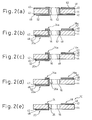
- the remaining dry resist 50 is removed, as shown in Fig. 2(a), and parts of the copper layer 48 and the copper foils 40, 42 exposed by the masking layer 52 are etched with an etching liquid capable of etching the copper layer 48 and removed, as shown in Fig. 2(b) and Fig. 3(a).
- a conductor pattern portion 18a to be the signal conductor pattern 18 (which may be hereinafter referred merely to a "pattern 18")
- another conductor pattern portion 20a to be the other conductor pattern 20 (which may be hereinafter referred merely to a "pattern 20a")
- a bonding conductor pattern portion 24a to be the bonding conductor pattern 24 (which may be hereinafter referred merely to a "pattern 24a”) are formed, as shown in Figs. 2(b) and Fig. 3(a).
- each of the patterns 20a and each of the patterns 24a are electrically connected to each other by means of the copper layer 48 formed all over the inner surface of the cavity 16 and the masking layer 52 covering all over the copper layer 48.
- inner surface conductor sections 26 must be formed on the inner surface of the cavity 16.
- a patterning is applied to the portions of the masking layer 52 on which the inner surface conductor sections 26 are to be formed.
- the masking layer 52 on the inner surface of the cavity 16 is partially removed by means of a mechanical means so that it remains in conformity with a shape of the inner surface conductor section 26, as shown in Fig. 2(c) and Fig. 3(b).
- the mechanical means used for this purpose may be a router wherein a drill having a cutting section at a tip end thereof is movable rightward and leftward as well as upward and downward while rotating.
- a router wherein a drill having a cutting section at a tip end thereof is movable rightward and leftward as well as upward and downward while rotating.
- the drill instead of moving the drill, the drill may be rotated at a predetermined position but the resinous board 44 may be moved to remove the masking layer 52.
- the inner surface conductor pattern portion 26a to be the inner surface conductor section 26, (which may be hereinafter referred merely to as a "pattern 26a") for electrically connecting the pattern 20a with the pattern 24a is formed on the inner surface of the cavity 16, as shown in Figs. 2(d) and Fig. 3(c).
- burrs generated when the masking layer 52 is partially removed by the mechanical means are also removable.
- the masking layer 52 still left on the patterns 18a, 20a, 24a and 26a thus formed is removed by an etching operation, whereby a resinous board 10 is obtained wherein the bonding conductor patterns 24 formed on one side thereof are connected to the other conductor patterns 20 formed on the other side of the resinous board 10 by means of the inner surface conductor sections 26 formed on inner surface of the cavity 16 of the resinous board 10.
- an alkaline etching liquid capable of dissolving tin without dissolving copper such as sodium hydroxide can be used so that only the masking layer 52 is removed without etching the copper layer 48 forming the respective patterns.
- the burrs which may be generated when the masking layer 52 is partially removed by the mechanical means, are also removed.
- burrs or the like generated in the masking layer 52 and/or the copper layer 48 when the masking layer 52 is partially removed are completely eliminated by the two etching operations applied after the partial removal of the masking layer 52 by the mechanical means, resulting in smooth and even inner surface conductor sections 26.
- a burr generated in the copper layer 48 had an average height of 42.57 ⁇ m (standard deviation; 31.46 ⁇ m) as measured at 108 locations.
- the inner surface conductor section 26 were formed by a process shown in Figs. 1(a) to 3(c), no such burrs were recognized.
- the masking layer 52 is formed of tin (Sn) in the above-described embodiment, it may be formed of solder which also is insoluble in the etching liquid for etching the copper layer 48.
- the masking layer 52 of solder is also formed by electroplating.
- the inner surface conductor section 26 in the above-mentioned embodiment is formed to have a width equal to that of the bonding conductor pattern 24, it may be much narrower than the pattern width of the bonding conductor pattern 24 provided it is electrically insulated from the adjacent inner surface conductor section 26.
- the other conductor pattern 20 may be formed so as to have a width larger than that of the signal conductor pattern 18 so that it is usable as a power source conductor pattern or a ground conductor pattern.
- the copper layer 48 may be used as it is without applying patterning for etching thereon.
- the conductor patterns formed on the opposite sides of the resinous board 10 are connected with each other via the inner surface conductor sections 26 formed on the inner surface of the cavity 16, it is also possible to apply the present invention to a multi-layer resinous board formed of a plurality of superposed resinous board components, each having conductor patterns.
- the electrical connection between conductor patterns formed in the inner layers of the multi-layer resinous board and those formed on one outer surface of the uppermost resinous board component is made via inner surface conductor sections formed on the inner surface of the cavity of the multi-layer resinous board.
- a substrate for a semiconductor device is easily obtainable, wherein selected ones of conductor patterns formed on one side of a resinous board having a cavity are connected to other patterns formed on the other side of this resinous board via the inner surface conductor sections.
- a substrate for a semiconductor device, carrying signal conductor patterns densely arranged on one side of the resinous board is easily provided.
Applications Claiming Priority (2)
| Application Number | Priority Date | Filing Date | Title |
|---|---|---|---|
| JP36704098A JP3453318B2 (ja) | 1998-12-24 | 1998-12-24 | 半導体装置用基板の製造方法 |
| JP36704098 | 1998-12-24 |
Publications (2)
| Publication Number | Publication Date |
|---|---|
| EP1014436A2 true EP1014436A2 (fr) | 2000-06-28 |
| EP1014436A3 EP1014436A3 (fr) | 2001-07-11 |
Family
ID=18488317
Family Applications (1)
| Application Number | Title | Priority Date | Filing Date |
|---|---|---|---|
| EP99310230A Withdrawn EP1014436A3 (fr) | 1998-12-24 | 1999-12-17 | Methode de fabrication d'une substrate |
Country Status (3)
| Country | Link |
|---|---|
| EP (1) | EP1014436A3 (fr) |
| JP (1) | JP3453318B2 (fr) |
| KR (1) | KR100601899B1 (fr) |
Families Citing this family (2)
| Publication number | Priority date | Publication date | Assignee | Title |
|---|---|---|---|---|
| JP5000446B2 (ja) * | 2007-10-01 | 2012-08-15 | 日本メクトロン株式会社 | プリント配線板の製造方法 |
| KR102268385B1 (ko) * | 2014-08-14 | 2021-06-23 | 삼성전기주식회사 | 인쇄회로기판 및 인쇄회로기판의 제조 방법 |
Citations (5)
| Publication number | Priority date | Publication date | Assignee | Title |
|---|---|---|---|---|
| DE3046346A1 (de) * | 1980-12-09 | 1982-07-15 | Amerigo de 6072 Dreieich Masi | Verfahren zur herstellung von elektrischen leiterplatten und vorrichtung zur durchfuehrung des verfahrens |
| US4543715A (en) * | 1983-02-28 | 1985-10-01 | Allied Corporation | Method of forming vertical traces on printed circuit board |
| DE3732249A1 (de) * | 1987-09-24 | 1989-04-13 | Siemens Ag | Verfahren zur herstellung von dreidimensionalen leiterplatten |
| EP0463763A2 (fr) * | 1990-06-22 | 1992-01-02 | Digital Equipment Corporation | Empaquetage semi-conducteur et procédé avec une métallisation du type à emballage |
| US5825084A (en) * | 1996-08-22 | 1998-10-20 | Express Packaging Systems, Inc. | Single-core two-side substrate with u-strip and co-planar signal traces, and power and ground planes through split-wrap-around (SWA) or split-via-connections (SVC) for packaging IC devices |
-
1998
- 1998-12-24 JP JP36704098A patent/JP3453318B2/ja not_active Expired - Fee Related
-
1999
- 1999-12-17 EP EP99310230A patent/EP1014436A3/fr not_active Withdrawn
- 1999-12-23 KR KR1019990060848A patent/KR100601899B1/ko not_active IP Right Cessation
Patent Citations (5)
| Publication number | Priority date | Publication date | Assignee | Title |
|---|---|---|---|---|
| DE3046346A1 (de) * | 1980-12-09 | 1982-07-15 | Amerigo de 6072 Dreieich Masi | Verfahren zur herstellung von elektrischen leiterplatten und vorrichtung zur durchfuehrung des verfahrens |
| US4543715A (en) * | 1983-02-28 | 1985-10-01 | Allied Corporation | Method of forming vertical traces on printed circuit board |
| DE3732249A1 (de) * | 1987-09-24 | 1989-04-13 | Siemens Ag | Verfahren zur herstellung von dreidimensionalen leiterplatten |
| EP0463763A2 (fr) * | 1990-06-22 | 1992-01-02 | Digital Equipment Corporation | Empaquetage semi-conducteur et procédé avec une métallisation du type à emballage |
| US5825084A (en) * | 1996-08-22 | 1998-10-20 | Express Packaging Systems, Inc. | Single-core two-side substrate with u-strip and co-planar signal traces, and power and ground planes through split-wrap-around (SWA) or split-via-connections (SVC) for packaging IC devices |
Also Published As
| Publication number | Publication date |
|---|---|
| EP1014436A3 (fr) | 2001-07-11 |
| KR100601899B1 (ko) | 2006-07-14 |
| KR20000048357A (ko) | 2000-07-25 |
| JP2000195985A (ja) | 2000-07-14 |
| JP3453318B2 (ja) | 2003-10-06 |
Similar Documents
| Publication | Publication Date | Title |
|---|---|---|
| US7256495B2 (en) | Package substrate manufactured using electrolytic leadless plating process, and method for manufacturing the same | |
| KR100499003B1 (ko) | 도금 인입선을 사용하지 않는 패키지 기판 및 그 제조 방법 | |
| US20110042128A1 (en) | Coreless packaging substrate and method for fabricating the same | |
| US20060180346A1 (en) | High aspect ratio plated through holes in a printed circuit board | |
| US5257452A (en) | Methods of recovering a multi-layer printed circuit board | |
| EP1951012B1 (fr) | Procédé de fabrication d'une carte de circuit en utilisant un électro-placage | |
| KR100751984B1 (ko) | 전자 부품의 제조 방법 및 전자 부품 | |
| KR20010007271A (ko) | 반도체소자 탑재용 중계기판의 제조방법 | |
| EP1146780B1 (fr) | Panneau à circuit et son procédé de fabrication | |
| US6651324B1 (en) | Process for manufacture of printed circuit boards with thick copper power circuitry and thin copper signal circuitry on the same layer | |
| EP1014436A2 (fr) | Methode de fabrication d'une substrate | |
| JP3770895B2 (ja) | 電解めっきを利用した配線基板の製造方法 | |
| JP2000091722A (ja) | プリント配線板及びその製造方法 | |
| KR100630913B1 (ko) | 인쇄회로기판의 제조방법 | |
| JP3759755B2 (ja) | 恒久的接続のために電気回路の上に隆起した金属接点を作成する方法 | |
| KR101063620B1 (ko) | 다층 인쇄회로기판 및 그의 제조방법 | |
| JP2795475B2 (ja) | プリント配線板及びその製造方法 | |
| JPH0336319B2 (fr) | ||
| JPH08186357A (ja) | プリント配線板及びその製造方法 | |
| JP3812006B2 (ja) | 多層プリント配線板の製造方法 | |
| JP3323114B2 (ja) | 密着力強化穴を有する表面実装用パッド | |
| JPH0748583B2 (ja) | 高密度プリント配線板の電気検査治具板の製造方法 | |
| JPH09321436A (ja) | 多層プリント基板及びその製造方法 | |
| JP2007180592A (ja) | 電子部品搭載用基板及びその製造方法 | |
| JPH06152148A (ja) | 多層印刷配線板の修復方法 |
Legal Events
| Date | Code | Title | Description |
|---|---|---|---|
| PUAI | Public reference made under article 153(3) epc to a published international application that has entered the european phase |
Free format text: ORIGINAL CODE: 0009012 |
|
| AK | Designated contracting states |
Kind code of ref document: A2 Designated state(s): DE FR GB |
|
| AX | Request for extension of the european patent |
Free format text: AL;LT;LV;MK;RO;SI |
|
| PUAL | Search report despatched |
Free format text: ORIGINAL CODE: 0009013 |
|
| AK | Designated contracting states |
Kind code of ref document: A3 Designated state(s): AT BE CH CY DE DK ES FI FR GB GR IE IT LI LU MC NL PT SE |
|
| AX | Request for extension of the european patent |
Free format text: AL;LT;LV;MK;RO;SI |
|
| RIC1 | Information provided on ipc code assigned before grant |
Free format text: 7H 01L 21/48 A, 7H 01L 23/498 B |
|
| 17P | Request for examination filed |
Effective date: 20011227 |
|
| AKX | Designation fees paid |
Free format text: DE FR GB |
|
| 17Q | First examination report despatched |
Effective date: 20080715 |
|
| STAA | Information on the status of an ep patent application or granted ep patent |
Free format text: STATUS: THE APPLICATION IS DEEMED TO BE WITHDRAWN |
|
| 18D | Application deemed to be withdrawn |
Effective date: 20081126 |