EP1511181B1 - Verzerrungskompensator - Google Patents
Verzerrungskompensator Download PDFInfo
- Publication number
- EP1511181B1 EP1511181B1 EP02730843A EP02730843A EP1511181B1 EP 1511181 B1 EP1511181 B1 EP 1511181B1 EP 02730843 A EP02730843 A EP 02730843A EP 02730843 A EP02730843 A EP 02730843A EP 1511181 B1 EP1511181 B1 EP 1511181B1
- Authority
- EP
- European Patent Office
- Prior art keywords
- distortion compensation
- distortion
- signal
- phase
- compensation coefficient
- Prior art date
- Legal status (The legal status is an assumption and is not a legal conclusion. Google has not performed a legal analysis and makes no representation as to the accuracy of the status listed.)
- Expired - Lifetime
Links
Images





Classifications
-
- H—ELECTRICITY
- H03—ELECTRONIC CIRCUITRY
- H03F—AMPLIFIERS
- H03F1/00—Details of amplifiers with only discharge tubes, only semiconductor devices or only unspecified devices as amplifying elements
- H03F1/32—Modifications of amplifiers to reduce non-linear distortion
- H03F1/3241—Modifications of amplifiers to reduce non-linear distortion using predistortion circuits
- H03F1/3294—Acting on the real and imaginary components of the input signal
-
- H—ELECTRICITY
- H03—ELECTRONIC CIRCUITRY
- H03F—AMPLIFIERS
- H03F1/00—Details of amplifiers with only discharge tubes, only semiconductor devices or only unspecified devices as amplifying elements
- H03F1/32—Modifications of amplifiers to reduce non-linear distortion
- H03F1/3241—Modifications of amplifiers to reduce non-linear distortion using predistortion circuits
- H03F1/3247—Modifications of amplifiers to reduce non-linear distortion using predistortion circuits using feedback acting on predistortion circuits
-
- H—ELECTRICITY
- H03—ELECTRONIC CIRCUITRY
- H03F—AMPLIFIERS
- H03F1/00—Details of amplifiers with only discharge tubes, only semiconductor devices or only unspecified devices as amplifying elements
- H03F1/32—Modifications of amplifiers to reduce non-linear distortion
- H03F1/3241—Modifications of amplifiers to reduce non-linear distortion using predistortion circuits
- H03F1/3282—Acting on the phase and the amplitude of the input signal
- H03F1/3288—Acting on the phase and the amplitude of the input signal to compensate phase shift as a function of the amplitude
-
- H—ELECTRICITY
- H04—ELECTRIC COMMUNICATION TECHNIQUE
- H04L—TRANSMISSION OF DIGITAL INFORMATION, e.g. TELEGRAPHIC COMMUNICATION
- H04L27/00—Modulated-carrier systems
- H04L27/32—Carrier systems characterised by combinations of two or more of the types covered by groups H04L27/02, H04L27/10, H04L27/18 or H04L27/26
- H04L27/34—Amplitude- and phase-modulated carrier systems, e.g. quadrature-amplitude modulated carrier systems
- H04L27/36—Modulator circuits; Transmitter circuits
- H04L27/366—Arrangements for compensating undesirable properties of the transmission path between the modulator and the demodulator
- H04L27/367—Arrangements for compensating undesirable properties of the transmission path between the modulator and the demodulator using predistortion
- H04L27/368—Arrangements for compensating undesirable properties of the transmission path between the modulator and the demodulator using predistortion adaptive predistortion
-
- H—ELECTRICITY
- H03—ELECTRONIC CIRCUITRY
- H03F—AMPLIFIERS
- H03F2201/00—Indexing scheme relating to details of amplifiers with only discharge tubes, only semiconductor devices or only unspecified devices as amplifying elements covered by H03F1/00
- H03F2201/32—Indexing scheme relating to modifications of amplifiers to reduce non-linear distortion
- H03F2201/3233—Adaptive predistortion using lookup table, e.g. memory, RAM, ROM, LUT, to generate the predistortion
Definitions
- the present invention relates to an adaptive predistortor type distortion compensator which operates an adaptive algorithm so that errors of a reference signal and a feedback signal outputted from an amplifier may be minimized in order to calculate a distortion compensation coefficient and increase the efficiency of the amplifier by compensating the nonlinear distortion of the amplifier using this distortion compensation coefficient.
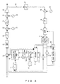
- Fig. 1 shows an example of the basic configuration of a conventional adaptive predistortor type distortion compensator.
- An input baseband signal (1) is a complex baseband signal comprising I signal and Q signal.
- the input baseband signal (1) is multiplied by a distortion compensation coefficient in the multiplier 18 and is inputted to the quadrature modulator 19.
- a signal modulated by the quadrature modulator 19 is converted into an analog signal by the digital-to-analog converter 20.
- This analog signal is multiplied by a periodic wave of the local oscillator 21 in the multiplier 22, and is converted into a signal of an intermediate frequency (IF).
- IF intermediate frequency
- the signal of the intermediate frequency generated in this way passes through the band-pass filter 23; is multiplied by the periodic wave of the local oscillator 24 in the multiplier 25; is converted into a radio frequency (RF); is amplified and transmitted by the (power) amplifier 26.
- the input baseband signal (1) is converted into a power value by the power computing unit 11, and is used to index a distortion compensation coefficient from the distortion compensation table 10 which stores the distortion compensation coefficient in a memory using the power value of the input baseband signal (1) as an address.
- the input baseband signal (1) is also inputted as a reference signal (3) to the subtractor 16 which obtains an error signal e (t) from a feedback signal (2) and the input baseband signal .
- the output from the amplifier 26 is separated by the feedback path 32 and is attenuated by the attenuator 27.
- the output is multiplied by the periodic wave of the local oscillator 28 in the multiplier 29 and is returned to the intermediate frequency.
- the output is converted into a digital signal in the analog-to-digital converter 30; is demodulated in the quadrature demodulator 31; and I signal and Q signal are generated.
- I signal and Q signal pass through the low-pass filter 17, and are inputted to the rotator 13, and at the same time are also inputted to the subtractor 16 as a feedback signal (2).
- An error signal e (t) which is a difference between a reference signal (3) and a signal in which a feedback signal (2) from the amplifier 26 is attenuated to a reasonable amplitude by the attenuator 27 (which is shown by ATT in Fig. 1 ) is computed as a digital signal.
- a clipped LMS algorithm is used as an adaptive algorithm, and the distortion compensation coefficient h n (p) (p is the power of the reference signal) is updated for the quantitized amplitudes of the signals using e(t) by the following expression.
- y(t) indicates a feedback signal
- * indicates a complex conjugate
- j indicates an imaginary unit
- ⁇ indicates an update step of a distortion compensation coefficient.
- This computing is conducted by the rotator 13, update storage unit 12, multiplier 15, adder 14 and distortion compensation table 10 shown in Fig. 1 .
- This algorithm is the one in which a circuit configuration is simplified by multiplying the part to be multiplied by an error signal in which complex multiplication is required in an ordinary LMS algorithm by det [h n-1 (p)] det [y (t) *] i.e. by conducting only the phase rotation of 0, ⁇ /2, ⁇ and 3 ⁇ /2.
- US 2001/0005402 A1 concerns a technology in which when the delay time of a reference signal and feedback signal exceeds a predetermined time, distortion compensation operation is stopped and an appropriate delay time is reestablished.
- US 2001/0007435 A1 concerns a technology which stops the calculation of distortion compensation coefficient when the difference between the power of a transmission signal multiplied by k and the power of the signal after distortion compensation exceeds a threshold value.
- the present invention provides a distortion compensator in accordance with claim 1.
- the present invention also provides a distortion compensation method in accordance with claim 11.
- the present invention provides a distortion compensator which can secure a proper operation of a distortion compensator even when the signal level of a reference signal or a feedback signal becomes 0 (zero) or only a noise component due to a fault, etc. of the distortion compensator.
- the distortion compensator even if information necessary for distortion compensation is not correctly obtained due to a fault, etc. of the distortion compensator, any improper distortion compensation operation can be prevented. Therefore, the operation of the distortion compensator is stable, and the distortion compensator can perform distortion compensation with higher accuracy and perform better-quality communications.
- the deterioration of distortion compensation characteristics is prevented by detecting the abnormality and stopping each function. Described below is the embodiment according to each function.
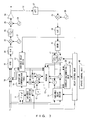
- Fig. 2 shows the embodiment of the present invention in a distortion compensator including a phase adjustment circuit.
- Fig. 1 shows the same reference number or mark to the same constituent shown in Fig. 1 to omit a detailed description of the constituent.
- the automatic phase adjustment is carried out by detecting the phase difference between a reference signal and a feedback signal in the phase control circuit 40 and adjusting, in the quadrature demodulator 31, the phase of a periodic wave multiplied for demodulation by a signal transmitted through the feedback path 32.
- Fig. 3 shows the block diagram of the phase control circuit.
- the update control unit 48 shown in Fig. 3 either of the reference signal, the feedback signal, the address of the distortion compensation table, or the phase value is inputted to the phase update judgement circuit 46. That is to say, the update control unit 48 uses the input of said circuit which the distortion compensation circuit requires to compensate distortion and instructs to make the phase update judgement circuit 46 implement phase updating or to stop implementing phase updating.
- the phase update information obtained as the result of computing the correlation value is inputted to an updown counter 45.
- the updown counter 45 the count value counts up or down each time phase update information is inputted, and when the count value becomes a given value, the updown counter 45 instructs the phase update judgement circuit 46 to update the phase value.
- the phase update judgement circuit 46 instructs the phase counter 47 to update the phase value of a predetermined step based on the instruction from the updown counter 45. At that time, the phase update judgement circuit 46 judges the value of the phase update instruction inputted from the updown counter 45 is plus or minus, and instructs the phase counter 47 to set the phase value to plus or minus. Also, the phase update judgement circuit 46 instructs the phase counter 47 to update the phase value, and inputs a reset signal to the updown counter 45. Therefore, the updown counter 45 continues to implement counting until the phase value becomes a predetermined value each time the phase value is updated.
- the phase counter 47 adds or decreases the phase value by a given step in accordance with the instruction from the phase update judgement circuit 46. Then, the phase counter 47 outputs the phase value thus obtained and makes the quadrature demodulator adjust the phase.
- Fig. 4 to Fig. 6 are flowcharts showing the processing which the update control unit 48 implements.
- a reference signal In the case of a reference signal, a feedback signal, an address of the distortion compensation table (a power value of an input baseband signal), if the size of the signals is equal to or less than a certain threshold, and in the case of a phase value, if the difference from the previous phase value is equal to or more than a certain threshold, the phase value is prevented from becoming an abnormal value by stopping the phase updating.
- Fig. 4 is a flowchart showing the processes of detecting the abnormality of a reference signal, a feedback signal, or an address of the distortion compensation table.
- x is the signal value of the reference signal, the signal value of the feedback signal, or the address value of the distortion compensation table.
- Step S1 it is judged whether the absolute value of x is smaller than the threshold. This is to judge whether x is 0 (zero) or only a noise component, and the threshold is what should be determined appropriately by the person of ordinary skill in the art.
- Step S1 the update control unit 48 conducts an ordinary operation in Step S2, and proceeds to Step S4. If the judgement in Step S1 is Yes, since some abnormality has been detected, the update control unit 48 stops the phase control function in Step S3 and holds the signal value or address value before the abnormality has been detected, and proceeds to Step S4.
- Step S4 the time interval in which the abnormality of the signal value or address value is detected is calculated by a timer (not shown in Fig. 4 ) which the update control unit 48 has. When this timer times out, the update control unit 48 proceeds to Step S1 again and repeats the processing. Several seconds to several tens of seconds are considered as the time in which the timer times out.
- Fig. 5 is a flowchart showing the processes of detecting the abnormality of a phase value.
- Step S10 it is judged whether the absolute value of the difference between the phase value stored in the previous processing and the phase value acquired in the current processing is larger than the threshold.
- This threshold is what should be set appropriately by the person of ordinary skill in the art.
- Step S10 the update control unit 48 conducts an ordinary operation in Step S11, and proceeds to Step S13. If the judgement in Step S10 is Yes, since some abnormality has been detected, the update control unit 48 stops the phase control function and holds the previous phase and proceeds to Step S13. In Step S13, when the timer measures time and times out, the update control unit 48 goes back to Step S10 and repeats the processing. The time in which the timer times out is the same as described above.
- Fig. 6 is a flowchart showing the processes of monitoring the feedback signal which is x and which has become extremely large due to a fault, etc. of an amplifier.
- Step S15 it is judged whether the absolute value of x is larger than the threshold.
- This threshold is also what is appropriately determined as an upper-limit predictable value by the person of ordinary skill in the art as a feedback signal value. If the judgement in Step S15 is No, the update control unit 48 conducts an ordinary operation in Step S16, and proceeds to Step S18. If the judgement in Step S15 is Yes, the update control unit 48 stops the phase control function and holds the previous phase and proceeds to Step S18. In Step S18, the timer measures the time interval for monitoring the feedback signal in the same way as the previous processing.
- the signal value, address value and phase value which frequently change are monitored in every given time using this timer, and when some abnormality is detected, implementing an inappropriate distortion compensation can be prevented by stopping the automatic phase control function.
- the update control unit 48 implements phase updating based on the signals received, and processes the signals successively in the order of the signal inputted. If any abnormality is detected in any of the signals inputted, the update control unit 48 is made to stop the phase control function.
- the phase of a reference signal is made to conform to the phase of a feedback signal, but in fact, there is a slight error, and this error is taken out by an error signal and is reflected to the updating of a distortion compensation coefficient. Therefore, even if the phase of the reference signal conforms to the phase of the feedback signal, the phases of the input baseband signal and the radio frequency signal do not conform. However, since the phase of a radio frequency signal which is transmitted by a radio frequency rotates randomly during the transmission in the air, the phase of a radio frequency signal should be adjusted on the receiver side and then should be received. Therefore, the phase of the input baseband signal and the phase of the radio frequency signal to be transmitted do not necessarily need to conform to each other.
- an error signal is used to update a distortion compensation coefficient.
- the time correlation between a reference signal and a feedback signal needs to conform to obtain a correct error signal. Then, before implementing the distortion compensation operation, the correlation between the reference signal and the feedback signal is calculated while changing the delay of the reference signal, and the timing in which the output power value becomes maximum is detected to adjust the delay. This method is called automatic delay adjustment.
- Fig. 7 shows the block diagram of an adaptive predistortor type distortion compensator in which automatic delay adjustment is considered.
- the same reference number or mark is given to the same constituent as in Fig. 1 to omit a detailed explanation of the constituent.
- Fig. 8 shows further details of the processing flow of the delay control.
- Step S20 the tap of the FIR is conformed to the symbol point. In other words, the delay which is given to the feedback signal by the FIR filter is made 0. Then, in Step S21, the correlation x between the reference signal and the feedback signal is calculated, and in Step S22, whether x is larger than max_x which is stored in a memory as the maximum correlation value is judged. If the judgement in Step S22 is No, the processing proceeds to Step S24. If the judgement in Step S22 is Yes, x is substituted for max_x, and the delay value "delay" when the correlation value is x is substituted for max_delay, and then the processing proceeds to Step S24.
- Step S24 the delay value "delay” is incremented by+1, and in step S25, whether the delay value "delay" is maximum is judged. If the judgement in Step S25 is No, the processing goes back to Step S21 and the processing is repeated. If the judgement in Step S25 is Yes, the processing proceeds to Step S26. In Step S26, the delay value of max_delay is set to the variable delay device. Now, the setting of the variable delay device is completed.
- Step S27 the correlationxbetween the reference signal and the feedback signal is calculated.
- Step S28 whether the maximum value max_x of up to the previous correlation is larger than x is judged. If the judgement in Step S28 is No, the processing proceeds to Step S30, and if the judgement in Step S28 is Yes, the processing proceeds to Step S29. In Step S29, x is substituted for max_x, and the tap value "tap" is substituted for max_tap, and the processing proceeds to Step S30.
- step S30 tap is incremented by +1, and in Step S31, whether the tap is maximum is judged. If the judgement in Step S31 is No, the processing proceeds to Step S27, and if the judgement in Step S31 is Yes, a coefficient corresponding to max_tap is set to the FIR filter in Step S32. Now, the setting of the delayvalue is completed.
- the update control unit 48 shown in Fig. 7 inputs any out of the reference signal, feedback signal, address of the distortion compensation table, and phase value of the automatic phase adjustment to the delay control unit 54.
- the update control unit 48 makes the variable delay device 51 to 53 and the FIR filter (low-pass filter 17) stop the setting operation for adjusting the timing, and uses a value immediately before the setting operation is stopped.
- the delay value is prevented from becoming an abnormal value.
- a signal has frequency characteristics according to the characteristics of the analog part of an adaptive predistortor type distortion compensator, particularly the characteristics of the band-pass filter which is inserted into an IF frequency.
- the compensation characteristics of a linearizer can be improved.
- Fig. 9 shows an example of the configuration of the adaptive predistortor type distortion compensator when the embodiment of the present invention is applied to the configuration using an equalizer.
- the same number or mark is given to the same constituents as in Fig. 1 to omit a detailed explanation of the constituent.
- a complex filter 57 shown in Fig. 9 plays the role of the equalizer.
- the method of setting the complex filter 57 is described as follows.
- the update control unit 48 shown in Fig. 9 inputs any of the reference signal, feedback signal, address of the distortion compensation table, or phase value of the automatic phase adjustment to the filter coefficient setting unit 56.
- the update control unit 48 stops the operation of setting a new filter coefficient to the complex filter, and uses the previous value.
- the flowchart showing this processing is as shown in Fig. 4 to Fig. 6 .
- the function for stopping said operation and the function for performing an ordinary operation shown in Fig. 4 to Fig. 6 are to update and set the filter coefficient of the complex filter which is the equalizer.
- Fig. 10 shows the adaptive predistortor type distortion compensator to which a function for protecting the values in the distortion compensation table is added.
- Fig. 10 the same number or mark is given to the same constituent as in Fig. 1 to omit a detailed explanation of the constituent.
- the update control unit 48 shown in Fig. 10 inputs any out of the reference signal, feedback signal, address of the distortion compensation table, or phase value of the automatic phase adjustment to an update stop control unit 60.
- the update control unit 48 stops the update of the distortion compensation table, and uses previous values.
- the function for stopping said operation and the function for performing an ordinary operation are to control the output of a write enable signal of the distortion compensation table 10 which is a memory such as prohibition of writing and permission of writing of the distortion compensation table 10.
- Fig. 11 shows an example of the configuration of the distortion compensator including all the four functions of automatic phase control, automatic delay control, equalizer control and distortion compensation table control. The same number or mark is given to the same constituent as in Fig. 2 , Fig. 7 , Fig. 9 and Fig. 10 to omit a detailed explanation of the constituent.
- Fig. 11 the operation of each function is as described above.
- the stop of the four functions i.e. automatic phase control, automatic delay control, equalizer control, and distortion compensation table control means to prevent the distortion compensation coefficient from being improperly updated. Therefore, when something wrong is detected in the input of the distortion compensation unit while monitoring the input of the distortion compensation unit which comprises the distortion compensation table 10, adder 14, multiplier 15, update step value storage unit 12, rotator 13, and subtractor 16, the update control unit 48 implements the operation of stopping each function.
- the adaptive predistortor type distortion compensator can reduce a negative influence that results in the distortion compensation characteristics being deteriorated rapidly, by immediately detecting something wrong when there is such abnormality with a signal due to a fault, etc. of the compensator, and stopping each function properly.
Landscapes
- Engineering & Computer Science (AREA)
- Physics & Mathematics (AREA)
- Nonlinear Science (AREA)
- Power Engineering (AREA)
- Computer Networks & Wireless Communication (AREA)
- Signal Processing (AREA)
- Amplifiers (AREA)
- Transmitters (AREA)
Claims (20)
- Verzerrungskompensator, der die Nichtlinearität eines Verstärkers kompensiert, der in einer Kommunikationsvorrichtung enthalten ist, mit:einem Verzerrungskompensationskoeffizienten-Speichermittel (10) zum Speichern eines Verzerrungskompensationskoeffizienten, der die Verzerrung durch Multiplizieren eines Eingangsbasisbandsignals (1) kompensiert;einem Verzerrungskompensationskoeffizienten-Aktualisierungsmittel (12, 13, 14, 15) zum Aktualisieren des Verzcrrungskompensationskoeffizienten; undeinem Verzerrungskompensationsstoppmittel (48) zum Stoppen einer Verzerrungskompensationsoperation, wenn die Eingabe an einer Einheit, die wenigstens das Verzerrungskompensationskoeffizienten-Speichermittel und das Verzcrrungskompensationskoeffizienten-Aktualisierungsmittel umfasst, 0 wird oder lediglich eine Rauschkomponente ist.
- Verzerrungskompensator nach Anspruch 1, bei dem
die Eingabe für die Einheit (10, 12, 13, 14, 15) eines ist von dem durch Trennung des Eingangsbasisbandsignals erhaltenen Referenzsignal (3), dem durch Rückführung der Ausgabe des Verstärkers (26) erhaltenen Rückführungssignal (2), der Adresse zum Lesen des Verzerrungskompensationskoeffizienten von dem Verzerrungskompensationskoeffizienten-Speichermittel (10) und dem Phasenwert der Phasensteuerung (40), die ausgeführt wird, um die Phase des Referenzsignals an die Phase des Rückführungssignals anzupassen. - Verzerrungskompensator nach Anspruch 1, bei dem
das Verzerrungskompensationskoeffizienten-Aktualisierungsmittel (12, 13, 14, 15) ein Phasendifferenzkompensationsmittel (40, 31) hat, zum Kompensieren der Differenz von Phasen zwischen dem durch Trennung des Eingangsbasisbandsignals (1) erhaltenen Referenzsignal (3) und dem durch Rückführung der Ausgabe des verstärkers (26) erhaltenen Rückführungssignal (2); und
das Verzerrungskompensationsstoppmittel (48) die automatische Aktualisierungsfunktion der Phasendifferenz des Phasendifferenzkompensationsmittels stoppt. - Verzerrungskompensator nach Anspruch 3, bei dem
das Phasendifferenzkompensationsmittel (40, 31) die Phase einer periodischen Welle, die mit dem Signal von dem Verstärker (26) multipliziert wird, um das Rückführungssignal (2) zu erhalten, in dem Demodulator (31) steuert, der in einem Rückführungsweg vorgesehen ist. - Verzerrungskompensalor nach Anspruch 1, bei dem
das Verzerrungskompensationskoeffizienten-Aktualisierungsmittel ein Mittel (50) umfasst, zum Erfassen eines Fehlersignals von dem durch Trennung des Eingangsbasisbandsignals (1) erhaltenen Referenzsignal (3) und dem durch Rückführung der Ausgabe des Verstärkers (26) erhaltenen Rückführungssignal, sowie ein Verzögerungsbetragseinstellmittel (51, 52, 53, 54), zum Einstellen des Verzögerungsbetrags des Referenzsignals und des Rückführungssignals; und
das Verzerrungskompensationsstoppmittel (48) die automatische Verzogerungsbetragseinstellfunktion des Verzögerungsbetragseinstellmittels (51, 52, 53, 54) stoppt. - Verzerrungskompensator nach Anspruch 5, bei dem
das Verzögerungsbetragseinstellmittel (51, 52, 53, 54) ein Verzögerungsmittel (51, 52, 53) hat, das die Verzögerung in Takteinheiten einstellt, und ein Digitalfilter (17), das die Verzögerung einstellt, die kleiner gleich einem Taktzyklus ist. - Verzerrungskompensator nach Anspruch 1, bei dem
das Verzerrungskompensationskoeffizienten-Aktualisierungsmittel ein Entzerrermittel (57) hat, zum Entzerren der Verzerrung des Signals, das durch das analoge Mittel (23) geliefert wird, das die Verarbeitung unter Verwendung eines analogen Signals implementiert; und
das Verzerrungskompensationsstoppmittel die automatische Entzerrungsfunktion des Entzerrermittels stoppt. - Verzerrungskompensator nach Anspruch 7, bei dem
das Entzerrermittel (57) ein komplexes Filter ist. - Verzerrungskompensator nach Anspruch 7, bei dem
das Entzerrermittel eine Entzerrungsverarbeitung durch Messen (55) des Nachbarkanal-Verlustleistungsverhältnisses eines Rückführungssignals implementiert. - Verzerrungskompensator nach Anspruch 1, der ein Schreibsteuermittel (60) zum Steuern des Schreibens im Verzerrungskompensationskoeffizienten-Speichermittel (10) hat, bei dem
das Verzerrungskompensationsstoppmittel (48) das Schreiben im Verzerrungskompensationskoeffizienten-Speichermittel (10) durch das Schreibsteuermittel unmöglich macht. - Verzerrungskompensationsverfahren, das die Nichtlinearität eines Verstärkers (26) kompensiert, der in einer Kommunikationsvorrichtung enthalten ist, mit den Schritten:Speichern (10) eines Verzerrungskompensationskoeffizienten, der die Verzerrung durch Multiplizieren eines Eingangsbasisbandsignals kompensiert;Aktualisieren (12, 13, 14, 15) des Verzerrungskompensationskoeffizienten; undStoppen (48) einer Verzerrungskompensationsoperation, wenn die Eingabe bei einem Verzerrungskompensationsschritt, bei dem wenigstens der Verzerrungskompensationskoeffizienten-Speicherschritt und der Verzerrungskompensationskoeffizienten-Aktualisierungsschritt ausgeführt werden, 0 wird oder lediglich eine Rauschkomponente ist.
- Verzerrungskompensationsverfahren nach Anspruch 11, bei dem
die Eingabe bei dem Verzerrungskompensationsschritt eines ist von dem durch Trennung des Eingangsbasisbandsignals (1) erhaltenen Referenzsignal (3), dem durch Rückführung der Ausgabe des Verstärkers (26) erhaltenen Rückführungssignal (2), der Adresse zum Lesen des Verzerrungskompensationskoeffizienten von dem Verzerrungskompensationskoeffizienten-Speicherschritt und dem Phasenwert der Phasensteuerung (40), die ausgeführt wird, um die Phase des Referenzsignals an die Phase des Rückführungssignals anzupassen. - Verzerrungskompensation nach Anspruch 11, bei der
der verzerrungskompensationskoeffizienten-Aktualisierungsschritt einen Phasendifferenzkompensationsschritt hat, zum Kompensieren der Differenz von Phasen zwischen dem durch Trennung des Eingangsbasisbandsignals erhaltenen Referenzsignal (3) und dem durch Rückführung der Ausgabe des Verstärkers (26) erhaltenen Rückführungssignal (2); und
der Verzerrungskompensationsstoppschritt (48) die automatische Aktualisierungsfunktion der Phasendifferenz des Phasendifferenzkompensationsschrittes stoppt. - Verzerrungskompensationsverfahren nach Anspruch 13, bei dem
der Phasendifferenzkompensationsschritt die Phase einer periodischen Welle, die mit dem Signal von dem Verstärker (26) multipliziert wird, um das Rückführungssignal (2) zu erhalten, in dem Demodulator (31) steuert, der in einem Rückführungsweg vorgesehen ist. - Verzerrungskompensation nach Anspruch 11, bei der
der Verzerrungskompensationskoeffizienten-Aktualisierungsschritt die Schritte (50) umfasst zum Erfassen eines Fehlersignals von dem durch Trennung des Eingangsbasisbandsignals (1) erhaltenen Referenzsignal (3) und dem durch Rückführung der Ausgabe des Verstärkers (26) erhaltenen Rückführungssignal (2) sowie zum Einstellen des Verzögerungsbetrags des Referenzsignals und des Hückführungssignals; und
der Verzerrungskompensationsstoppschritt (48) die automatische Verzögerungsbetragseinstellfunktion des Verzögerungsbetragseinstellschrittes stoppt. - Verzerrungskompensationsverfahren nach Anspruch 15, bei dem
der Verzögerungsbetragseinstellschritt eine Verzögerungseinheit (51, 52, 53) hat, die die Verzögerung in Takteinheiten einstellt, und ein Digitalfilter (17), das die Verzögerung einstellt, die kleiner gleich einem Taktzyklus ist. - Verzerrungskompensation nach Anspruch 11, bei der
der Verzerrungskompensationskoeffizienten-Aktualisierungsschritt den Schritt umfasst zum Entzerren (57) der Verzerrung des Signals, das durch eine analoge Einheit (23) geliefer wird, die die Verarbeitung unter Verwendung eines analogen Signals implementiert; und
der Verzerrungskompensationsstoppschritt die automatische Entzerrungsfunktion des Entzerrungsschrittes stoppt. - Verzerrungskompensationsverfahren nach Anspruch 17, bei dem
beim Entzerrungsschritt ein komplexes Filter (57) verwendet wird. - Verzerrungskompensation nach Anspruch 17, bei der
beim Entzerrungsschritt eine Entzerrungsverarbeitung durch Messen (55) des Nachbarkanal-Verlustleistunqsverhältnisses eines Rückführungssignals implementiert wird. - Verzerrungskompensationsverfahren nach Anspruch 11, das den Schritt zum Steuern des Schreibens beim Verzerrungskompensationskoeffizienten-Speicherschritt (10) umfasst, bei dem
der Verzerrungskompensationsstoppschritt (48) das Schreiben beim Verzerrungskompensationskoeffizienten-Speicherschritt (10) durch den Schreibsteuerschritt (60) unmöglich macht.
Applications Claiming Priority (1)
| Application Number | Priority Date | Filing Date | Title |
|---|---|---|---|
| PCT/JP2002/005372 WO2003103166A1 (ja) | 2002-05-31 | 2002-05-31 | 歪補償装置 |
Publications (3)
| Publication Number | Publication Date |
|---|---|
| EP1511181A1 EP1511181A1 (de) | 2005-03-02 |
| EP1511181A4 EP1511181A4 (de) | 2005-07-27 |
| EP1511181B1 true EP1511181B1 (de) | 2009-12-09 |
Family
ID=29606644
Family Applications (1)
| Application Number | Title | Priority Date | Filing Date |
|---|---|---|---|
| EP02730843A Expired - Lifetime EP1511181B1 (de) | 2002-05-31 | 2002-05-31 | Verzerrungskompensator |
Country Status (5)
| Country | Link |
|---|---|
| US (1) | US7106133B2 (de) |
| EP (1) | EP1511181B1 (de) |
| JP (1) | JP3957077B2 (de) |
| DE (1) | DE60234724D1 (de) |
| WO (1) | WO2003103166A1 (de) |
Families Citing this family (46)
| Publication number | Priority date | Publication date | Assignee | Title |
|---|---|---|---|---|
| JP4961661B2 (ja) * | 2004-09-10 | 2012-06-27 | 株式会社日立製作所 | ディジタルプリディストーション型送信機および無線基地局 |
| CN101023578B (zh) * | 2004-09-21 | 2010-04-21 | 株式会社日立国际电气 | 失真补偿放大装置 |
| GB2421648B (en) * | 2004-12-23 | 2009-01-07 | Zetex Plc | Amplifier fault detection circuit |
| JP4555702B2 (ja) * | 2005-02-21 | 2010-10-06 | 富士通株式会社 | 歪補償装置 |
| JP4652091B2 (ja) * | 2005-03-16 | 2011-03-16 | 富士通株式会社 | 歪補償装置 |
| JP4308163B2 (ja) * | 2005-03-22 | 2009-08-05 | 富士通株式会社 | 歪補償装置 |
| EP1914884B8 (de) * | 2005-07-29 | 2016-09-21 | Fujitsu Ltd. | Verzögerungs-regulierungseinrichtung |
| JP4323470B2 (ja) * | 2005-08-08 | 2009-09-02 | 富士通株式会社 | アドレス生成装置およびその方法 |
| JP4299819B2 (ja) | 2005-08-17 | 2009-07-22 | 富士通株式会社 | 歪補償装置及び歪補償方法 |
| JPWO2007049474A1 (ja) * | 2005-10-24 | 2009-04-30 | 株式会社日立国際電気 | プリディストーション方式歪補償増幅装置 |
| JP4648214B2 (ja) | 2006-02-14 | 2011-03-09 | 富士通株式会社 | 呼制御装置および呼制御方法 |
| JP4863729B2 (ja) | 2006-02-14 | 2012-01-25 | 富士通株式会社 | 歪補償装置及び歪補償方法 |
| JP4617265B2 (ja) | 2006-02-14 | 2011-01-19 | 富士通株式会社 | 歪補償装置及び歪補償方法 |
| JP4617270B2 (ja) * | 2006-03-27 | 2011-01-19 | 株式会社日立国際電気 | 送信機 |
| JP4755937B2 (ja) | 2006-04-17 | 2011-08-24 | 富士通株式会社 | 歪補償装置及び歪補償方法 |
| JP5034319B2 (ja) * | 2006-05-26 | 2012-09-26 | 富士通株式会社 | 歪補償装置及び歪補償方法 |
| JP5242024B2 (ja) * | 2006-06-08 | 2013-07-24 | 株式会社東芝 | 歪補償装置、増幅装置、送信装置、歪補償方法 |
| WO2008035439A1 (en) * | 2006-09-22 | 2008-03-27 | Panasonic Corporation | Distortion compensating circuit and method for controlling the same |
| JP2008205759A (ja) * | 2007-02-20 | 2008-09-04 | Japan Radio Co Ltd | 歪補償装置 |
| US7957707B2 (en) * | 2007-03-30 | 2011-06-07 | Freescale Semiconductor, Inc. | Systems, apparatus and method for performing digital pre-distortion based on lookup table gain values |
| WO2008147908A1 (en) * | 2007-05-25 | 2008-12-04 | Rambus Inc. | A multi-antenna beam-forming system for transmitting constant envelope signals decomposed from a variable envelope signal |
| US8482462B2 (en) | 2007-05-25 | 2013-07-09 | Rambus Inc. | Multi-antenna beam-forming system for transmitting constant envelope signals decomposed from a variable envelope signal |
| WO2008146355A1 (ja) * | 2007-05-28 | 2008-12-04 | Panasonic Corporation | 歪補償装置 |
| US8068574B2 (en) * | 2007-05-31 | 2011-11-29 | Freescale Semiconductor, Inc. | Systems, apparatus, and methods for performing digital pre-distortion with feedback signal adjustment |
| JP5141694B2 (ja) * | 2007-07-19 | 2013-02-13 | 富士通株式会社 | 非線形歪み補償付き増幅装置 |
| JP5218173B2 (ja) | 2009-03-12 | 2013-06-26 | 富士通株式会社 | 無線送信機の位相補正装置、無線送信機の歪補償装置 |
| WO2010113213A1 (ja) * | 2009-03-31 | 2010-10-07 | 富士通株式会社 | 位相調整回路の自己試験装置及び方法 |
| JP2010258597A (ja) | 2009-04-22 | 2010-11-11 | Fujitsu Ltd | 電力増幅器の歪補償装置、電力増幅器の歪補償装置における故障検出方法 |
| US8774314B2 (en) | 2009-06-23 | 2014-07-08 | Qualcomm Incorporated | Transmitter architectures |
| JP5158034B2 (ja) * | 2009-08-12 | 2013-03-06 | 富士通株式会社 | 無線装置及び信号処理方法 |
| US20110143697A1 (en) * | 2009-12-11 | 2011-06-16 | Qualcomm Incorporated | Separate i and q baseband predistortion in direct conversion transmitters |
| US8880010B2 (en) | 2009-12-30 | 2014-11-04 | Qualcomm Incorporated | Dual-loop transmit noise cancellation |
| JP5672728B2 (ja) * | 2010-03-12 | 2015-02-18 | 富士通株式会社 | 無線装置、歪補償装置及び歪補償方法 |
| JP5488073B2 (ja) * | 2010-03-12 | 2014-05-14 | 富士通株式会社 | 無線装置、歪補償装置及び歪補償方法 |
| JP5434818B2 (ja) * | 2010-06-25 | 2014-03-05 | 富士通株式会社 | 歪補償装置、歪補償方法及び無線通信装置 |
| JP5673238B2 (ja) * | 2011-03-10 | 2015-02-18 | 富士通株式会社 | 電力増幅装置、送信機及び電力増幅装置制御方法 |
| CN103634252B (zh) * | 2012-08-20 | 2016-08-17 | 富士通株式会社 | 一种数字预失真系数的更新控制方法和装置 |
| US8995571B2 (en) * | 2013-03-14 | 2015-03-31 | Analog Devices Global | Baseband digital pre-distortion architecture |
| US9680422B2 (en) * | 2013-03-27 | 2017-06-13 | Qualcomm Incorporated | Power amplifier signal compensation |
| US20150092825A1 (en) * | 2013-09-27 | 2015-04-02 | Qualcomm Incorporated | Self-test using internal feedback for transmit signal quality estimation |
| JP6446911B2 (ja) * | 2014-08-25 | 2019-01-09 | 富士通株式会社 | 歪補償方法、歪補償装置、及び歪補償プログラム |
| JP6413795B2 (ja) * | 2015-01-23 | 2018-10-31 | 富士通株式会社 | 歪補償装置 |
| JP2017069649A (ja) | 2015-09-28 | 2017-04-06 | 富士通株式会社 | 無線装置 |
| JP6943104B2 (ja) * | 2017-09-15 | 2021-09-29 | 日本電気株式会社 | 増幅装置、破損検出装置および破損検出方法 |
| US10454509B2 (en) | 2018-03-13 | 2019-10-22 | Qualcomm Incorporated | Communication circuit including a transmitter |
| JP2020141379A (ja) | 2019-03-01 | 2020-09-03 | 富士通株式会社 | 歪み補償装置及び歪み補償方法 |
Family Cites Families (16)
| Publication number | Priority date | Publication date | Assignee | Title |
|---|---|---|---|---|
| JPH0968733A (ja) | 1995-09-04 | 1997-03-11 | Nikon Corp | ブレ補正機構,カメラ,レンズ装置及びボディ装置 |
| US5903823A (en) * | 1995-09-19 | 1999-05-11 | Fujitsu Limited | Radio apparatus with distortion compensating function |
| FR2746564B1 (fr) * | 1996-03-22 | 1998-06-05 | Matra Communication | Procede pour corriger des non-linearites d'un amplificateur, et emetteur radio mettant en oeuvre un tel procede |
| US5892397A (en) * | 1996-03-29 | 1999-04-06 | Spectrian | Adaptive compensation of RF amplifier distortion by injecting predistortion signal derived from respectively different functions of input signal amplitude |
| JP3360029B2 (ja) | 1998-07-13 | 2002-12-24 | 松下電器産業株式会社 | 歪補償用アドレス発生器,歪補償回路および送信歪補償付き送信機 |
| JP2000036767A (ja) | 1998-07-17 | 2000-02-02 | Hitachi Denshi Ltd | 送信機 |
| US6275685B1 (en) * | 1998-12-10 | 2001-08-14 | Nortel Networks Limited | Linear amplifier arrangement |
| JP2000228643A (ja) | 1999-02-08 | 2000-08-15 | Matsushita Electric Ind Co Ltd | 非線形歪補償装置 |
| JP4014343B2 (ja) * | 1999-12-28 | 2007-11-28 | 富士通株式会社 | 歪補償装置 |
| JP4183364B2 (ja) | 1999-12-28 | 2008-11-19 | 富士通株式会社 | 歪補償装置 |
| JP2001284976A (ja) * | 2000-03-29 | 2001-10-12 | Matsushita Electric Ind Co Ltd | アダプティブプリディストーション歪補償方法及び装置 |
| JP4306933B2 (ja) | 2000-06-29 | 2009-08-05 | パナソニック株式会社 | 送信装置 |
| JP2002111401A (ja) * | 2000-10-03 | 2002-04-12 | Fujitsu Ltd | 信号の歪補償装置および歪補償方法 |
| WO2002101919A1 (fr) | 2001-06-12 | 2002-12-19 | Fujitsu Limited | Dispositif de compensation de distorsion |
| JP4015455B2 (ja) | 2002-03-29 | 2007-11-28 | 富士通株式会社 | 歪補償装置 |
| JP3874688B2 (ja) | 2002-03-29 | 2007-01-31 | 富士通株式会社 | 歪補償装置 |
-
2002
- 2002-05-31 EP EP02730843A patent/EP1511181B1/de not_active Expired - Lifetime
- 2002-05-31 WO PCT/JP2002/005372 patent/WO2003103166A1/ja not_active Ceased
- 2002-05-31 DE DE60234724T patent/DE60234724D1/de not_active Expired - Lifetime
- 2002-05-31 JP JP2004510129A patent/JP3957077B2/ja not_active Expired - Fee Related
-
2004
- 2004-11-30 US US10/999,747 patent/US7106133B2/en not_active Expired - Fee Related
Also Published As
| Publication number | Publication date |
|---|---|
| EP1511181A4 (de) | 2005-07-27 |
| US20050073361A1 (en) | 2005-04-07 |
| WO2003103166A1 (ja) | 2003-12-11 |
| JP3957077B2 (ja) | 2007-08-08 |
| EP1511181A1 (de) | 2005-03-02 |
| JPWO2003103166A1 (ja) | 2005-10-06 |
| US7106133B2 (en) | 2006-09-12 |
| DE60234724D1 (de) | 2010-01-21 |
Similar Documents
| Publication | Publication Date | Title |
|---|---|---|
| US7106133B2 (en) | Distortion compensator | |
| US7024608B2 (en) | Transmitting method and transmitting apparatus | |
| US7034613B2 (en) | Adaptive predistortion for transmit system with gain, phase and delay adjustments | |
| KR100857359B1 (ko) | 데이터수신기의 전처리장치 및 비선형왜곡 등화방법 | |
| KR100864558B1 (ko) | 왜곡 보상 장치 및 왜곡 보상 방법 | |
| US20080095264A1 (en) | Device and method for pre-distorting a base-band digital signal | |
| US7986930B2 (en) | IQ imbalance image suppression in presence of unknown phase shift | |
| EP1860770B1 (de) | Entzerrerschaltung und Methode | |
| WO2002032067A1 (en) | Method for automatic frequency control | |
| EP1450482B1 (de) | Schaltung und Verfahren zum Kompensieren der nonlinearen Verzerrung eines Leistungsverstärkers | |
| US8411797B2 (en) | Frequency offset compensation in a digital frequency shift keying receiver | |
| CN101453437B (zh) | 频率偏移估计方法、自动频率控制方法及信号收发器 | |
| US7327191B2 (en) | Distortion compensating apparatus and method | |
| US20050101258A1 (en) | Distortion compensation apparatus | |
| US6294960B1 (en) | Phase lock loop circuit using signal estimator | |
| EP1869779B1 (de) | Empfänger zum empfang und zur demodulierung eines frequenzmodulierten rf-signals und betriebsverfahren dafür | |
| EP1916773B1 (de) | Gleichstrom-Offsetkorrektureinrichtung und Verfahren dafür | |
| US20040049717A1 (en) | Frequency error detector and combiner in receiving end of mobile communication system | |
| JP3355147B2 (ja) | 自動周波数制御方式 | |
| JPS5813036A (ja) | 非線形歪み除去回路 |
Legal Events
| Date | Code | Title | Description |
|---|---|---|---|
| PUAI | Public reference made under article 153(3) epc to a published international application that has entered the european phase |
Free format text: ORIGINAL CODE: 0009012 |
|
| 17P | Request for examination filed |
Effective date: 20041222 |
|
| AK | Designated contracting states |
Kind code of ref document: A1 Designated state(s): DE FR GB IT |
|
| A4 | Supplementary search report drawn up and despatched |
Effective date: 20050614 |
|
| RIC1 | Information provided on ipc code assigned before grant |
Ipc: 7H 03F 1/32 B Ipc: 7H 04L 27/36 B Ipc: 7H 04L 27/00 B Ipc: 7H 04B 1/04 A |
|
| 17Q | First examination report despatched |
Effective date: 20061006 |
|
| GRAP | Despatch of communication of intention to grant a patent |
Free format text: ORIGINAL CODE: EPIDOSNIGR1 |
|
| RTI1 | Title (correction) |
Free format text: DISTORTION COMPENSATOR |
|
| GRAS | Grant fee paid |
Free format text: ORIGINAL CODE: EPIDOSNIGR3 |
|
| GRAA | (expected) grant |
Free format text: ORIGINAL CODE: 0009210 |
|
| AK | Designated contracting states |
Kind code of ref document: B1 Designated state(s): DE FR GB IT |
|
| REG | Reference to a national code |
Ref country code: GB Ref legal event code: FG4D |
|
| REF | Corresponds to: |
Ref document number: 60234724 Country of ref document: DE Date of ref document: 20100121 Kind code of ref document: P |
|
| PLBE | No opposition filed within time limit |
Free format text: ORIGINAL CODE: 0009261 |
|
| STAA | Information on the status of an ep patent application or granted ep patent |
Free format text: STATUS: NO OPPOSITION FILED WITHIN TIME LIMIT |
|
| 26N | No opposition filed |
Effective date: 20100910 |
|
| PGFP | Annual fee paid to national office [announced via postgrant information from national office to epo] |
Ref country code: GB Payment date: 20140528 Year of fee payment: 13 |
|
| PGFP | Annual fee paid to national office [announced via postgrant information from national office to epo] |
Ref country code: IT Payment date: 20140522 Year of fee payment: 13 Ref country code: FR Payment date: 20140509 Year of fee payment: 13 Ref country code: DE Payment date: 20140528 Year of fee payment: 13 |
|
| REG | Reference to a national code |
Ref country code: DE Ref legal event code: R119 Ref document number: 60234724 Country of ref document: DE |
|
| GBPC | Gb: european patent ceased through non-payment of renewal fee |
Effective date: 20150531 |
|
| PG25 | Lapsed in a contracting state [announced via postgrant information from national office to epo] |
Ref country code: IT Free format text: LAPSE BECAUSE OF NON-PAYMENT OF DUE FEES Effective date: 20150531 |
|
| REG | Reference to a national code |
Ref country code: FR Ref legal event code: ST Effective date: 20160129 |
|
| PG25 | Lapsed in a contracting state [announced via postgrant information from national office to epo] |
Ref country code: DE Free format text: LAPSE BECAUSE OF NON-PAYMENT OF DUE FEES Effective date: 20151201 Ref country code: GB Free format text: LAPSE BECAUSE OF NON-PAYMENT OF DUE FEES Effective date: 20150531 |
|
| PG25 | Lapsed in a contracting state [announced via postgrant information from national office to epo] |
Ref country code: FR Free format text: LAPSE BECAUSE OF NON-PAYMENT OF DUE FEES Effective date: 20150601 |