EP1510355B1 - Datenaufzeichnungsmedium und herstellungsverfahren dafür - Google Patents
Datenaufzeichnungsmedium und herstellungsverfahren dafür Download PDFInfo
- Publication number
- EP1510355B1 EP1510355B1 EP03733031A EP03733031A EP1510355B1 EP 1510355 B1 EP1510355 B1 EP 1510355B1 EP 03733031 A EP03733031 A EP 03733031A EP 03733031 A EP03733031 A EP 03733031A EP 1510355 B1 EP1510355 B1 EP 1510355B1
- Authority
- EP
- European Patent Office
- Prior art keywords
- recording medium
- recording layer
- information recording
- nitride
- medium according
- Prior art date
- Legal status (The legal status is an assumption and is not a legal conclusion. Google has not performed a legal analysis and makes no representation as to the accuracy of the status listed.)
- Expired - Lifetime
Links
- 238000000034 method Methods 0.000 title claims description 24
- 230000008569 process Effects 0.000 title claims description 6
- 239000010410 layer Substances 0.000 claims description 230
- IJGRMHOSHXDMSA-UHFFFAOYSA-N Atomic nitrogen Chemical compound N#N IJGRMHOSHXDMSA-UHFFFAOYSA-N 0.000 claims description 101
- 150000004767 nitrides Chemical class 0.000 claims description 93
- 239000002184 metal Substances 0.000 claims description 63
- 229910052751 metal Inorganic materials 0.000 claims description 63
- 229910052757 nitrogen Inorganic materials 0.000 claims description 49
- 238000004544 sputter deposition Methods 0.000 claims description 32
- 239000000463 material Substances 0.000 claims description 26
- 239000000203 mixture Substances 0.000 claims description 24
- 239000012298 atmosphere Substances 0.000 claims description 22
- 238000005546 reactive sputtering Methods 0.000 claims description 21
- 239000000758 substrate Substances 0.000 claims description 21
- 150000001875 compounds Chemical class 0.000 claims description 16
- 239000000126 substance Substances 0.000 claims description 15
- 229910052718 tin Inorganic materials 0.000 claims description 13
- 229910052797 bismuth Inorganic materials 0.000 claims description 12
- 229910045601 alloy Inorganic materials 0.000 claims description 11
- 239000000956 alloy Substances 0.000 claims description 11
- 238000004519 manufacturing process Methods 0.000 claims description 11
- -1 at least of Bi Chemical class 0.000 claims description 8
- 229910052732 germanium Inorganic materials 0.000 claims description 7
- 229910044991 metal oxide Inorganic materials 0.000 claims description 7
- 229910052782 aluminium Inorganic materials 0.000 claims description 6
- 150000004706 metal oxides Chemical class 0.000 claims description 6
- 229910052710 silicon Inorganic materials 0.000 claims description 6
- 229910052742 iron Inorganic materials 0.000 claims description 5
- 229910052719 titanium Inorganic materials 0.000 claims description 5
- 229910052697 platinum Inorganic materials 0.000 claims description 4
- 229910052791 calcium Inorganic materials 0.000 claims description 3
- 229910052799 carbon Inorganic materials 0.000 claims description 3
- 229910052802 copper Inorganic materials 0.000 claims description 3
- 229910052735 hafnium Inorganic materials 0.000 claims description 3
- 229910052738 indium Inorganic materials 0.000 claims description 3
- 229910052741 iridium Inorganic materials 0.000 claims description 3
- 229910052749 magnesium Inorganic materials 0.000 claims description 3
- 229910052758 niobium Inorganic materials 0.000 claims description 3
- 229910052762 osmium Inorganic materials 0.000 claims description 3
- 229910052760 oxygen Inorganic materials 0.000 claims description 3
- 229910052702 rhenium Inorganic materials 0.000 claims description 3
- 229910052703 rhodium Inorganic materials 0.000 claims description 3
- 229910052707 ruthenium Inorganic materials 0.000 claims description 3
- 229910052706 scandium Inorganic materials 0.000 claims description 3
- 229910052709 silver Inorganic materials 0.000 claims description 3
- 229910052712 strontium Inorganic materials 0.000 claims description 3
- 229910052713 technetium Inorganic materials 0.000 claims description 3
- 229910052721 tungsten Inorganic materials 0.000 claims description 3
- 229910052720 vanadium Inorganic materials 0.000 claims description 3
- 229910052727 yttrium Inorganic materials 0.000 claims description 3
- 229910052725 zinc Inorganic materials 0.000 claims description 3
- 229910052726 zirconium Inorganic materials 0.000 claims description 3
- 239000012299 nitrogen atmosphere Substances 0.000 claims description 2
- 239000011241 protective layer Substances 0.000 claims description 2
- 239000012535 impurity Substances 0.000 claims 2
- 229910052714 tellurium Inorganic materials 0.000 claims 2
- 229910052716 thallium Inorganic materials 0.000 claims 1
- 230000003287 optical effect Effects 0.000 description 34
- 238000000151 deposition Methods 0.000 description 27
- 230000008021 deposition Effects 0.000 description 26
- 239000007789 gas Substances 0.000 description 25
- VYPSYNLAJGMNEJ-UHFFFAOYSA-N Silicium dioxide Chemical compound O=[Si]=O VYPSYNLAJGMNEJ-UHFFFAOYSA-N 0.000 description 19
- 229910052681 coesite Inorganic materials 0.000 description 15
- 229910052906 cristobalite Inorganic materials 0.000 description 15
- 239000000377 silicon dioxide Substances 0.000 description 15
- 229910052682 stishovite Inorganic materials 0.000 description 15
- 229910052905 tridymite Inorganic materials 0.000 description 15
- 238000010521 absorption reaction Methods 0.000 description 12
- WMWLMWRWZQELOS-UHFFFAOYSA-N bismuth(iii) oxide Chemical compound O=[Bi]O[Bi]=O WMWLMWRWZQELOS-UHFFFAOYSA-N 0.000 description 10
- 230000035945 sensitivity Effects 0.000 description 10
- ATJFFYVFTNAWJD-UHFFFAOYSA-N Tin Chemical compound [Sn] ATJFFYVFTNAWJD-UHFFFAOYSA-N 0.000 description 9
- 238000005979 thermal decomposition reaction Methods 0.000 description 9
- 230000000052 comparative effect Effects 0.000 description 8
- 238000000354 decomposition reaction Methods 0.000 description 8
- 229910001873 dinitrogen Inorganic materials 0.000 description 8
- 230000008018 melting Effects 0.000 description 7
- 238000002844 melting Methods 0.000 description 7
- YBMRDBCBODYGJE-UHFFFAOYSA-N germanium dioxide Chemical compound O=[Ge]=O YBMRDBCBODYGJE-UHFFFAOYSA-N 0.000 description 6
- 229920005668 polycarbonate resin Polymers 0.000 description 6
- 239000004431 polycarbonate resin Substances 0.000 description 6
- 238000004833 X-ray photoelectron spectroscopy Methods 0.000 description 5
- 150000002736 metal compounds Chemical class 0.000 description 5
- 229920005989 resin Polymers 0.000 description 5
- 239000011347 resin Substances 0.000 description 5
- 238000007792 addition Methods 0.000 description 4
- 238000006243 chemical reaction Methods 0.000 description 4
- 238000000926 separation method Methods 0.000 description 4
- PNEYBMLMFCGWSK-UHFFFAOYSA-N aluminium oxide Inorganic materials [O-2].[O-2].[O-2].[Al+3].[Al+3] PNEYBMLMFCGWSK-UHFFFAOYSA-N 0.000 description 3
- 229910052593 corundum Inorganic materials 0.000 description 3
- 238000001723 curing Methods 0.000 description 3
- 238000000113 differential scanning calorimetry Methods 0.000 description 3
- 230000000694 effects Effects 0.000 description 3
- 230000001678 irradiating effect Effects 0.000 description 3
- 238000005259 measurement Methods 0.000 description 3
- 239000000088 plastic resin Substances 0.000 description 3
- 230000003595 spectral effect Effects 0.000 description 3
- 229910001845 yogo sapphire Inorganic materials 0.000 description 3
- 239000004925 Acrylic resin Substances 0.000 description 2
- 229920000178 Acrylic resin Polymers 0.000 description 2
- 229910002616 GeOx Inorganic materials 0.000 description 2
- GWEVSGVZZGPLCZ-UHFFFAOYSA-N Titan oxide Chemical compound O=[Ti]=O GWEVSGVZZGPLCZ-UHFFFAOYSA-N 0.000 description 2
- MCMNRKCIXSYSNV-UHFFFAOYSA-N Zirconium dioxide Chemical compound O=[Zr]=O MCMNRKCIXSYSNV-UHFFFAOYSA-N 0.000 description 2
- 239000006096 absorbing agent Substances 0.000 description 2
- 239000000853 adhesive Substances 0.000 description 2
- 230000001070 adhesive effect Effects 0.000 description 2
- 238000004458 analytical method Methods 0.000 description 2
- 230000008859 change Effects 0.000 description 2
- QDOXWKRWXJOMAK-UHFFFAOYSA-N dichromium trioxide Chemical compound O=[Cr]O[Cr]=O QDOXWKRWXJOMAK-UHFFFAOYSA-N 0.000 description 2
- 239000003822 epoxy resin Substances 0.000 description 2
- 239000011521 glass Substances 0.000 description 2
- 230000006872 improvement Effects 0.000 description 2
- 150000001247 metal acetylides Chemical class 0.000 description 2
- 239000005300 metallic glass Substances 0.000 description 2
- 230000000704 physical effect Effects 0.000 description 2
- 229920000647 polyepoxide Polymers 0.000 description 2
- 229920005672 polyolefin resin Polymers 0.000 description 2
- 230000005855 radiation Effects 0.000 description 2
- XOLBLPGZBRYERU-UHFFFAOYSA-N tin dioxide Chemical compound O=[Sn]=O XOLBLPGZBRYERU-UHFFFAOYSA-N 0.000 description 2
- QHGNHLZPVBIIPX-UHFFFAOYSA-N tin(II) oxide Inorganic materials [Sn]=O QHGNHLZPVBIIPX-UHFFFAOYSA-N 0.000 description 2
- 238000007740 vapor deposition Methods 0.000 description 2
- 229910018069 Cu3N Inorganic materials 0.000 description 1
- 229910000705 Fe2N Inorganic materials 0.000 description 1
- 229910002668 Pd-Cu Inorganic materials 0.000 description 1
- 229910052581 Si3N4 Inorganic materials 0.000 description 1
- 229910003564 SiAlON Inorganic materials 0.000 description 1
- 229910004205 SiNX Inorganic materials 0.000 description 1
- 229910006898 SnSi Inorganic materials 0.000 description 1
- UCKMPCXJQFINFW-UHFFFAOYSA-N Sulphide Chemical compound [S-2] UCKMPCXJQFINFW-UHFFFAOYSA-N 0.000 description 1
- RZJQYRCNDBMIAG-UHFFFAOYSA-N [Cu].[Cu].[Cu].[Cu].[Cu].[Cu].[Cu].[Cu].[Cu].[Cu].[Cu].[Cu].[Cu].[Cu].[Cu].[Cu].[Cu].[Cu].[Zn].[Ag].[Ag].[Ag].[Ag].[Ag].[Ag].[Ag].[Ag].[Ag].[Ag].[Ag].[Ag].[Ag].[Ag].[Ag].[Ag].[Ag].[Ag].[Ag].[Ag].[Ag].[Ag].[Ag].[Ag].[Ag].[Ag].[Ag].[Ag].[Ag].[Ag].[Ag].[Ag].[Ag].[Ag].[Ag].[Ag].[Ag].[Ag].[Ag].[Ag].[Ag].[Ag].[Ag].[Ag].[Ag].[Ag].[Ag].[Ag].[Ag].[Ag].[Ag].[Ag].[Ag].[Ag].[Ag].[Ag].[Ag].[Ag].[Ag].[Ag].[Ag].[Ag].[Sn].[Sn].[Sn].[Sn].[Sn].[Sn].[Sn].[Sn].[Sn].[Sn].[Sn].[Sn].[Sn].[Sn].[Sn].[Sn].[Sn].[Sn] Chemical group [Cu].[Cu].[Cu].[Cu].[Cu].[Cu].[Cu].[Cu].[Cu].[Cu].[Cu].[Cu].[Cu].[Cu].[Cu].[Cu].[Cu].[Cu].[Zn].[Ag].[Ag].[Ag].[Ag].[Ag].[Ag].[Ag].[Ag].[Ag].[Ag].[Ag].[Ag].[Ag].[Ag].[Ag].[Ag].[Ag].[Ag].[Ag].[Ag].[Ag].[Ag].[Ag].[Ag].[Ag].[Ag].[Ag].[Ag].[Ag].[Ag].[Ag].[Ag].[Ag].[Ag].[Ag].[Ag].[Ag].[Ag].[Ag].[Ag].[Ag].[Ag].[Ag].[Ag].[Ag].[Ag].[Ag].[Ag].[Ag].[Ag].[Ag].[Ag].[Ag].[Ag].[Ag].[Ag].[Ag].[Ag].[Ag].[Ag].[Ag].[Ag].[Sn].[Sn].[Sn].[Sn].[Sn].[Sn].[Sn].[Sn].[Sn].[Sn].[Sn].[Sn].[Sn].[Sn].[Sn].[Sn].[Sn].[Sn] RZJQYRCNDBMIAG-UHFFFAOYSA-N 0.000 description 1
- 238000000149 argon plasma sintering Methods 0.000 description 1
- 230000008901 benefit Effects 0.000 description 1
- 230000005540 biological transmission Effects 0.000 description 1
- JCXGWMGPZLAOME-UHFFFAOYSA-N bismuth atom Chemical compound [Bi] JCXGWMGPZLAOME-UHFFFAOYSA-N 0.000 description 1
- 230000003139 buffering effect Effects 0.000 description 1
- 238000004040 coloring Methods 0.000 description 1
- 239000000470 constituent Substances 0.000 description 1
- 238000010276 construction Methods 0.000 description 1
- 238000005260 corrosion Methods 0.000 description 1
- 230000007797 corrosion Effects 0.000 description 1
- 230000002939 deleterious effect Effects 0.000 description 1
- 230000001419 dependent effect Effects 0.000 description 1
- 239000003989 dielectric material Substances 0.000 description 1
- 238000007598 dipping method Methods 0.000 description 1
- 239000006185 dispersion Substances 0.000 description 1
- 238000010894 electron beam technology Methods 0.000 description 1
- 230000007613 environmental effect Effects 0.000 description 1
- 239000003344 environmental pollutant Substances 0.000 description 1
- 230000001747 exhibiting effect Effects 0.000 description 1
- 238000002309 gasification Methods 0.000 description 1
- 230000009477 glass transition Effects 0.000 description 1
- 229910052737 gold Inorganic materials 0.000 description 1
- 238000010438 heat treatment Methods 0.000 description 1
- 239000011261 inert gas Substances 0.000 description 1
- 229910010272 inorganic material Inorganic materials 0.000 description 1
- 239000011147 inorganic material Substances 0.000 description 1
- 238000009413 insulation Methods 0.000 description 1
- 229910000765 intermetallic Inorganic materials 0.000 description 1
- 230000002427 irreversible effect Effects 0.000 description 1
- 238000003475 lamination Methods 0.000 description 1
- 230000031700 light absorption Effects 0.000 description 1
- 238000001755 magnetron sputter deposition Methods 0.000 description 1
- 239000000155 melt Substances 0.000 description 1
- 229910001092 metal group alloy Inorganic materials 0.000 description 1
- 150000002739 metals Chemical class 0.000 description 1
- 238000012986 modification Methods 0.000 description 1
- 230000004048 modification Effects 0.000 description 1
- 229910003465 moissanite Inorganic materials 0.000 description 1
- 125000000449 nitro group Chemical group [O-][N+](*)=O 0.000 description 1
- QJGQUHMNIGDVPM-UHFFFAOYSA-N nitrogen group Chemical group [N] QJGQUHMNIGDVPM-UHFFFAOYSA-N 0.000 description 1
- 239000011368 organic material Substances 0.000 description 1
- 238000012856 packing Methods 0.000 description 1
- 239000012071 phase Substances 0.000 description 1
- 239000012782 phase change material Substances 0.000 description 1
- 239000004033 plastic Substances 0.000 description 1
- 231100000614 poison Toxicity 0.000 description 1
- 230000007096 poisonous effect Effects 0.000 description 1
- 231100000719 pollutant Toxicity 0.000 description 1
- 238000004321 preservation Methods 0.000 description 1
- 230000001681 protective effect Effects 0.000 description 1
- 238000003847 radiation curing Methods 0.000 description 1
- 238000002310 reflectometry Methods 0.000 description 1
- 229910010271 silicon carbide Inorganic materials 0.000 description 1
- 238000007711 solidification Methods 0.000 description 1
- 230000008023 solidification Effects 0.000 description 1
- 229910052950 sphalerite Inorganic materials 0.000 description 1
- 238000009718 spray deposition Methods 0.000 description 1
- 238000003892 spreading Methods 0.000 description 1
- 230000007480 spreading Effects 0.000 description 1
- 238000005477 sputtering target Methods 0.000 description 1
- 238000003860 storage Methods 0.000 description 1
- OGIDPMRJRNCKJF-UHFFFAOYSA-N titanium oxide Inorganic materials [Ti]=O OGIDPMRJRNCKJF-UHFFFAOYSA-N 0.000 description 1
- 238000012546 transfer Methods 0.000 description 1
- 238000002834 transmittance Methods 0.000 description 1
- 238000000927 vapour-phase epitaxy Methods 0.000 description 1
- 229910052984 zinc sulfide Inorganic materials 0.000 description 1
Images

Classifications
-
- G—PHYSICS
- G11—INFORMATION STORAGE
- G11B—INFORMATION STORAGE BASED ON RELATIVE MOVEMENT BETWEEN RECORD CARRIER AND TRANSDUCER
- G11B7/00—Recording or reproducing by optical means, e.g. recording using a thermal beam of optical radiation by modifying optical properties or the physical structure, reproducing using an optical beam at lower power by sensing optical properties; Record carriers therefor
- G11B7/24—Record carriers characterised by shape, structure or physical properties, or by the selection of the material
- G11B7/26—Apparatus or processes specially adapted for the manufacture of record carriers
- G11B7/266—Sputtering or spin-coating layers
-
- B—PERFORMING OPERATIONS; TRANSPORTING
- B41—PRINTING; LINING MACHINES; TYPEWRITERS; STAMPS
- B41M—PRINTING, DUPLICATING, MARKING, OR COPYING PROCESSES; COLOUR PRINTING
- B41M5/00—Duplicating or marking methods; Sheet materials for use therein
- B41M5/26—Thermography ; Marking by high energetic means, e.g. laser otherwise than by burning, and characterised by the material used
-
- G—PHYSICS
- G11—INFORMATION STORAGE
- G11B—INFORMATION STORAGE BASED ON RELATIVE MOVEMENT BETWEEN RECORD CARRIER AND TRANSDUCER
- G11B7/00—Recording or reproducing by optical means, e.g. recording using a thermal beam of optical radiation by modifying optical properties or the physical structure, reproducing using an optical beam at lower power by sensing optical properties; Record carriers therefor
- G11B7/24—Record carriers characterised by shape, structure or physical properties, or by the selection of the material
- G11B7/241—Record carriers characterised by shape, structure or physical properties, or by the selection of the material characterised by the selection of the material
- G11B7/242—Record carriers characterised by shape, structure or physical properties, or by the selection of the material characterised by the selection of the material of recording layers
- G11B7/243—Record carriers characterised by shape, structure or physical properties, or by the selection of the material characterised by the selection of the material of recording layers comprising inorganic materials only, e.g. ablative layers
-
- G—PHYSICS
- G11—INFORMATION STORAGE
- G11B—INFORMATION STORAGE BASED ON RELATIVE MOVEMENT BETWEEN RECORD CARRIER AND TRANSDUCER
- G11B7/00—Recording or reproducing by optical means, e.g. recording using a thermal beam of optical radiation by modifying optical properties or the physical structure, reproducing using an optical beam at lower power by sensing optical properties; Record carriers therefor
- G11B7/24—Record carriers characterised by shape, structure or physical properties, or by the selection of the material
- G11B7/26—Apparatus or processes specially adapted for the manufacture of record carriers
-
- G—PHYSICS
- G11—INFORMATION STORAGE
- G11B—INFORMATION STORAGE BASED ON RELATIVE MOVEMENT BETWEEN RECORD CARRIER AND TRANSDUCER
- G11B7/00—Recording or reproducing by optical means, e.g. recording using a thermal beam of optical radiation by modifying optical properties or the physical structure, reproducing using an optical beam at lower power by sensing optical properties; Record carriers therefor
- G11B7/24—Record carriers characterised by shape, structure or physical properties, or by the selection of the material
- G11B7/241—Record carriers characterised by shape, structure or physical properties, or by the selection of the material characterised by the selection of the material
- G11B7/242—Record carriers characterised by shape, structure or physical properties, or by the selection of the material characterised by the selection of the material of recording layers
- G11B7/243—Record carriers characterised by shape, structure or physical properties, or by the selection of the material characterised by the selection of the material of recording layers comprising inorganic materials only, e.g. ablative layers
- G11B2007/24302—Metals or metalloids
- G11B2007/24306—Metals or metalloids transition metal elements of groups 3-10
-
- G—PHYSICS
- G11—INFORMATION STORAGE
- G11B—INFORMATION STORAGE BASED ON RELATIVE MOVEMENT BETWEEN RECORD CARRIER AND TRANSDUCER
- G11B7/00—Recording or reproducing by optical means, e.g. recording using a thermal beam of optical radiation by modifying optical properties or the physical structure, reproducing using an optical beam at lower power by sensing optical properties; Record carriers therefor
- G11B7/24—Record carriers characterised by shape, structure or physical properties, or by the selection of the material
- G11B7/241—Record carriers characterised by shape, structure or physical properties, or by the selection of the material characterised by the selection of the material
- G11B7/242—Record carriers characterised by shape, structure or physical properties, or by the selection of the material characterised by the selection of the material of recording layers
- G11B7/243—Record carriers characterised by shape, structure or physical properties, or by the selection of the material characterised by the selection of the material of recording layers comprising inorganic materials only, e.g. ablative layers
- G11B2007/24302—Metals or metalloids
- G11B2007/24312—Metals or metalloids group 14 elements (e.g. Si, Ge, Sn)
-
- G—PHYSICS
- G11—INFORMATION STORAGE
- G11B—INFORMATION STORAGE BASED ON RELATIVE MOVEMENT BETWEEN RECORD CARRIER AND TRANSDUCER
- G11B7/00—Recording or reproducing by optical means, e.g. recording using a thermal beam of optical radiation by modifying optical properties or the physical structure, reproducing using an optical beam at lower power by sensing optical properties; Record carriers therefor
- G11B7/24—Record carriers characterised by shape, structure or physical properties, or by the selection of the material
- G11B7/241—Record carriers characterised by shape, structure or physical properties, or by the selection of the material characterised by the selection of the material
- G11B7/242—Record carriers characterised by shape, structure or physical properties, or by the selection of the material characterised by the selection of the material of recording layers
- G11B7/243—Record carriers characterised by shape, structure or physical properties, or by the selection of the material characterised by the selection of the material of recording layers comprising inorganic materials only, e.g. ablative layers
- G11B2007/24302—Metals or metalloids
- G11B2007/24314—Metals or metalloids group 15 elements (e.g. Sb, Bi)
-
- G—PHYSICS
- G11—INFORMATION STORAGE
- G11B—INFORMATION STORAGE BASED ON RELATIVE MOVEMENT BETWEEN RECORD CARRIER AND TRANSDUCER
- G11B7/00—Recording or reproducing by optical means, e.g. recording using a thermal beam of optical radiation by modifying optical properties or the physical structure, reproducing using an optical beam at lower power by sensing optical properties; Record carriers therefor
- G11B7/24—Record carriers characterised by shape, structure or physical properties, or by the selection of the material
- G11B7/241—Record carriers characterised by shape, structure or physical properties, or by the selection of the material characterised by the selection of the material
- G11B7/242—Record carriers characterised by shape, structure or physical properties, or by the selection of the material characterised by the selection of the material of recording layers
- G11B7/243—Record carriers characterised by shape, structure or physical properties, or by the selection of the material characterised by the selection of the material of recording layers comprising inorganic materials only, e.g. ablative layers
- G11B2007/24318—Non-metallic elements
- G11B2007/24322—Nitrogen
-
- Y—GENERAL TAGGING OF NEW TECHNOLOGICAL DEVELOPMENTS; GENERAL TAGGING OF CROSS-SECTIONAL TECHNOLOGIES SPANNING OVER SEVERAL SECTIONS OF THE IPC; TECHNICAL SUBJECTS COVERED BY FORMER USPC CROSS-REFERENCE ART COLLECTIONS [XRACs] AND DIGESTS
- Y10—TECHNICAL SUBJECTS COVERED BY FORMER USPC
- Y10S—TECHNICAL SUBJECTS COVERED BY FORMER USPC CROSS-REFERENCE ART COLLECTIONS [XRACs] AND DIGESTS
- Y10S430/00—Radiation imagery chemistry: process, composition, or product thereof
- Y10S430/146—Laser beam
Definitions
- the present invention relates to an optical information recording medium such as an optical disc, an optical card and the like for recording/reproducing information by irradiating a light beam, and a method of manufacturing the same.
- DVD Digital Versatile Disc
- the DVD comes in different types: in addition to the DVD used exclusively for reproduction, the DVD-R (recordable) which uses an organic coloring material in the recording layer thereof to allow writing-once-reading-many, the DVD-RW (re-recordable) which uses a phase change material in the recording layer thereof to allow rewriting many times, and the like.
- an information recording medium according to claim 1 a method of manufacturing an information recording medium according to claim 18 and a target according to claim 20.
- an optical information recording medium which is constituted by forming a recording film, a reflecting film and a resin protective film on a transparent board made of plastic or glass.
- the recording film is obtained by sputtering SnN and metal as targets in a plasma of CH 4 gas by using a vacuum sputtering unit.
- Gas components such as CH 4 , C 2 H 4 , C 2 H 2 , or C 2 H 6 constitute chain-like organic substances of C and H in the film 2.
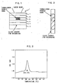
- An information recording medium 1 has a reflecting layer 3, a first dielectric layer 4, a recording layer 5 comprised essentially of a metal nitride as a major component, a second dielectric layer 6, and a light transparent covering layer 7 which are sequentially deposited on a main surface of a substrate 2.
- laser beams which are intensity-modulated in accordance with information, are irradiated through the light transparent covering layer 7 to heat the recording layer 5.
- the recording layer includes the metal nitride as a major component and has a low thermal conductivity
- the temperature of a laser beam irradiating portion rises due to thermal storage, the recording layer entirely or partly melts, the nitrogen content in the entire recording layer changes, a phase changes followed by changes in multiple reflection conditions of the irradiating portion during solidification, and a reflectance changes to become a recording mark, as shown in Figure 2. Therefore, it is conceivable that the percentage of nitride formed in the recording layer, which varies according to the nitrogen content, affects sensitivity. The variations in light reflectance occurring in this manner is irreversible, so that the recording layer can be used as a once-write-read-many type information medium. Upon reproduction, laser beams are irradiated to an area where the reflectance varied through the light transparent covering layer 7 to read an intensity variation in the reflective light and demodulate the read information.
- the recording layer 5 may be constituted by a substance selected from a group consisting of a metal nitride, a metal oxide, a metal carbide and a mixture of at least two thereof, e.g., one of Bi nitride, Sn nitride, Fe nitride, or Cu nitride, and a stable metal compound such as SiO 2 , Al 2 O 3 , GeO 2 , SnO, Bi 2 O 3 , SiC or the like.
- the recording layer made of the nitride insufficiently nitrided has a membranaceous quality similar to a thin amorphous metal film, its stiffness and stress become low aud its thermal conductivity increases.
- temperature rise is hard due to transverse dispersion of heat during heating.
- the thermal decomposition of nitrogen is expanded like a chain reaction, as a result, there occurs that for example the recording light spot makes a large mark greater than the light spot itself, as shown in Fig. 16. This phenomenon raises a problem of difficulty in control over the size and edge shape of mark to be recorded on the recording layer by the laser beam irradiation of purplish blue band.
- the recorded large mark is a serious problem to form a minute size mark having a width of 0.1-0.2 ⁇ m, though it is out of problem in CD case.
- the recording layer is constituted by a mixture of both a substance having a high stiffness and the difficult thermal decomposition characteristic and a nitride having the easy thermal decomposition characteristic.
- This mixture recording layer facilitates to control the thermal decomposition itself and to form the minute mark having a good shape.
- the substance having the difficult thermal decomposition characteristic is selected from materials having a high transmittance.
- the recording layer includes a low temperature decomposable nitride (nitrogen emission substance), a non-nitride (non-nitrided component in the nitride i.e., thermal absorber), and a high temperature decomposable compound (metal nitride or metal oxide or metal carbide or the mixture thereof i.e., thermal decomposition controller substance).
- the non-nitride will be realized as a non-nitrided component in the nitride composition constituting the recording layer. Therefore, the mixture of both the low temperature decomposable nitride having the non-nitrided component and the high temperature decomposable compound suffice for the recording layer of the recording medium.
- the thermal absorber i.e., non-nitrided component in the nitride of the recording layer exhibit temperature raise in the beam spot.
- the low temperature decomposable nitride is decomposed to emit nitrogen.
- (2) the recording layer is deformed by the emitted nitrogen.
- (2) is only of secondary recording mode.
- the deformation of the recording layer does not mainly contribute to the recording.
- the separation of nitrogen is likely to be hindered when the recording layer is suppressed with a storing pressure.
- the deformation of the recording layer should be allowed to a certain extent.
- the dielectric layer has a first role of buffering layer for the deformation of the recording layer when nitrogen comes out from the recording layer, a second role of adjusting layer for the optical characteristic, and a third role of thermal insulation against the effect of the metal reflecting layer radiating heat.
- the reflecting layer has functions both of the heat radiation and the enhancement of multiple-reflection for ensuring quantity of light. Thus the reflecting layer is not always provided.
- the low temperature decomposable nitride and the high temperature decomposable compound should be selected on the basis of a threshold temperature approximately 600 °C, for example, in comparison with temperature of decomposition for materials.
- Table 1 shows the decomposition temperatures of the various metal nitrides.
- Table Metal nitrides Decomposition temperatures (ca.°C) AgN 25 Na 3 N 200 BiN 220 Cu 3 N 300 Fe 2 N 350 SnN 380 GeN 600 or more GaN 1500 CrN 1600 Si 3 N 4 1900 AIN 2000 VN 2200 BN 2700 TiN 3300
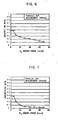
- the inventors have formed a film of BiN (recording layer) and analyzed the film with a differential scanning calorimetry.
- the BiN film has decomposed at approximately 220 °C as shown in Fig. 3. Further, the BiN filmhas exhibited a starting temperature of practice decomposing, approximately 180 °C which is lower than its decomposition temperature by 50-70 °C. It is considered in view of the allowable margin of error that the decomposition of BiN starts a temperature lower than its decomposition temperature by 50-100 °C.
- the inventors have formed optical discs having recording layers constituted by low temperature decomposable nitrides such as BiN, SnN and the like respectively and then evaluated them. As a result, it comes to a conclusion that BiN is superior to SnN as the low temperature decomposable nitride. However, the selection of SnN doesn't matter.
- Fig. 4 shows spectral characteristics curves of the recording layer employing BiN as a low temperature decomposable nitride resulting from ESCA (Electron Spectroscopy for Chemical Analysis or X-ray Photoelectron Spectroscopy).
- ESCA Electrode Spectroscopy for Chemical Analysis or X-ray Photoelectron Spectroscopy
- the high temperature decomposable compound is stable at a temperature of 600 °C or less and has a high transmissivity in the reading light beam irradiated to the optical disc and a high hardness to support the layer shape itself.
- Prospective metal compounds include metal nitride, metal oxide, metal carbide and the like as well as the mixture of at lest two thereof.
- the inventors have preformed the selection of layer component under the conditions of simultaneously sputterable material with the low temperature decomposable nitride while considering the environment except materials specified under the PRTR Law. As a result, the metal nitride stable at a high temperature, GeN, SiN, AlN, and TiN are prefable.
- the inventors have analyzed GeN, SiN, AlN, and TiN with the differential Scanning calorimetry and then recognized that no decomposing reaction of GeN occur at 500 °C.
- the inventors have formed optical discs having recording layers constituted by these high temperature decomposable nitrides respectively and then evaluated them. As a result, it comes to a conclusion that optical discs GeN>TiN>SiN>AlN are superior in this order on stableness.
- the use of GeN or TiN is preferable in optical characteristics.
- the stable metal compound at a high temperature includes stable metal oxides such as SiO 2 , Al 2 O 3 , GeO 2 , SnO, Bi 2 O 3 and the like, and stable metal carbides such as SiC and the like, as well as the mixture thereof.
- stable metal oxides such as SiO 2 , Al 2 O 3 , GeO 2 , SnO, Bi 2 O 3 and the like
- stable metal carbides such as SiC and the like, as well as the mixture thereof.
- SiC in carbides has a high thermal stableness and no melting under the atmospheric pressure.
- Table 2 shows melting points of oxides and carbide instead of decomposition temperatures, because the decomposition temperature melting point is higher than the melting point.
- the sublimating point is shown when the sublimating point is lower than the melting point.
- Table 2 Oxides or carbide Melting points (or sublimating point:SP) (°C) SiO 2 1710 Al 2 O 3 1990 or more GeO 2 1116 SnO 2 1127 Bi 2 O 3 820 TiO 2 1640 TiO 1750 ZnO 1725(SP) Cr 2 O 3 1990 CoO 1935 ZrO 2 2700 FeO 1370 CuO 1026 NiO 1998 BaO 1923 MnO 1650 MgO 2880 SiC 2200 or more(SP)
- the recording layer 5 of metal nitride can be deposited by various vapor deposition methods, it is preferably formed by a reactive sputtering method, and particularly it is preferably formed by the reactive sputtering method in an atmosphere including Ar and N 2 using a metal alloy target. This film forming process is preferable because the recording layer can be homogeneously formed at once.
- co-sputtering can be used for the process in which deposition simultaneously is performed using a plurality of targets or divided targets.
- a flow ratio Ar:N 2 in a sputtering atmosphere preferably ranges from 80:10 to 10:80, and more preferably from 80:10 to 30:60.
- the deposition rate tends to slow down as the amount of nitrogen gas introduced increases.
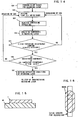
- a method of manufacturing the information recording medium of the embodiment includes, as shown in Fig. 5, a step S1 for loading a substrate on a sputtering device, and a recording layer forming step S4 for forming the recording layer by a reactive sputtering method using an alloy target comprising metal constituting a metal nitride, wherein the flow ratio Ar:N 2 in atmosphere including Ar and N 2 in the recording layer forming step is set to be within the range of 80:10 to 10: 80.
- the following procedure is preformed in the order as shown in Fig. 5.
- a reflecting layer is formed through the sputtering in an Ar gas atmosphere executed using a predetermined target (reflecting layer forming step S2).
- first dielectric layer forming step S3 a first dielectric layer is formed through the sputtering in an Ar gas atmosphere executed using another predetermined target.
- second dielectric layer forming step S5 a second dielectric layer is formed through the sputtering in an Ar gas atmosphere executed using another predetermined target.
- a covering layer is formed (S6).
- the recording layer 5 comprising the nitride composed of one or more elements of Bi, Sn, and either of the elements Ge, Ti, Si and Al for example, GeBiN, is capable of absorbing 10% or more of light in the vicinity of wavelength 405 nm at an unrecorded portion.
- the recording layer 5 can achieve such an absorption rate even in a short wave length area of, for example, 385 to 450 nm, thus making it possible to cope with high density recording using a short wave length laser light. Recording using violaceous laser can be performed with less recording energy by containing a metal nitride in the recording layer.
- the reactive sputtering allows control of the percentage of nitrogen in the metal nitride to change the absorption rate of the recording layer, the degree of freedom in designing of the medium is increased, a high reflectance and a suitable recording sensitivity are provided, and at the same time a high modulation degree, a low jitter, and a low cross talk can be implemented.
- inert gas such as Xe, Kr other than Ar can be added in the sputtering atmosphere.
- the metal used as a targets may be replaced by an off-stoichiometry material. Further, the use of the metal nitride target allows forming the above recording layer by using only Ar without N 2 gas.
- the thickness of the recording layer is determined as appropriate depending on the physical property of the recording layer, the physical property and thickness of the dielectric layer, it has been confirmed that a jitter can be removed sufficiently in case of the thickness being 5 to 40 nm, preferably 10 to 30 nm, for example 12 nm. If the thickness of the recording layer is thinner than 5 nm, it becomes difficult to enlarge the degree of modulation. If it is thicker than 40 nm, reflectance becomes insufficient due to light absorption by the recording layer.
- the substrate 2 is not particularly limited in dimension and shape thereof, it is in the form of disc and generally has a thickness of about 0.3 to 1.2 mm.
- a predetermined pattern such as a groove or the like can be provided on the substrate 2 as appropriate so as to guide a light beam for recording/reproduction such as for tracking, address, or the like.
- the light beam for recording/reproduction is usually irradiated within the groove.
- a groove can be provided on either or both of a light incident side and a light reflecting side of the substrate. Deposition can be performed from either side, the light incident or reflecting side.
- the substrate 2 may also be a card-form recording medium in addition to the disc shape.
- Dielectric layers 4, 6 are made of one or more of dielectrics, for example, an oxide, a nitride, or a sulf ide of SiO 2 , SiN X , ZnS, or the like, or a metallic compound such as various kinds of a metallic oxide, and a metallic carbide, and a mixture thereof, e.g., ZnS-SiO 2 , but are not limited to them in particular.
- a so-called LaSiON which contains La, Si, O, and N
- SiAlON dielectric which contains Si, Al, O, and N
- only a combination of materials which are not designated under the PRTR law can be selected.
- the dielectric layer may comprise a plurality of layers.
- the first dielectric layer on a light reflecting side functions to temporarily store heat generated by a laser light before it escapes to the reflecting layer to heat the recording layer sufficiently.
- the thickness of the dielectric layer is 40 nm or less, preferably 10 to 30 nm.
- a semitransparent film may be used for the reflecting layer.
- the semitransparent reflecting layer can be adapted to a multilayer write-once optical disc having a multilayered structure of recording layers so as to be disposed at a near side of the optical pickup.
- the lamination order without the reflecting layer is Substrate /Dielectric layer /Recording layer /Dielectric layer /Covering layer.
- the light transparent covering layer 7 In an information recording medium 1, a light for recording and a light for reproduction are irradiated to the recording layer 5 through a light transparent covering layer 7. Therefore, the light transparent covering layer 7 must be substantially transparent relative to the lights. Further, the light transparent covering layer 7 is provided so as to increase a mar resistance and a corrosion resistance, and preferably includes a variety of organic materials. In particular, it can comprise materials made by hardening a radiation curing type compound or a constituent thereof by radiation such as an electron beam, an ultraviolet ray, or the like.
- the present invention is applied to a single-sided recording type information recording medium
- the present invention is also applicable to a double-sided recording type information recording medium.
- the one-sided recording type can also be configured to comprise a protective layer which is adhered onto the light transparent covering layer 7.
- the layer structure of the recording medium is applicable as well as to the above composition and combination of the recording layer, to a variety of configurations, should they only meet the requirements of the present invention.
- configurations such as a configuration having no light transparent covering layer, a configuration having a layer of another material added other than a dielectric layer, a recording layer, and a reflecting layer, a configuration in which a recording layer further includes multilayers, a configuration having no reflecting layer, a configuration having two reflecting layers, a configuration having no light reflecting side substrate, a configuration having one or more recording medium configurations added at the positions of a light incident side substrate and a light reflecting side substrate to allow multilayer recording, and the like.
- a reflecting layer 3, a first dielectric layer 4, a recording layer 5, a second dielectric layer 6, and a light transparent covering layer 7 were formed in turn on the surface of a substrate 2 to make a sample of an optical disc as Example 1 which has a configuration shown in Fig. 1.
- a reflecting layer of Ag-Pd-Cu alloy having a thickness of 100 nm, and a first dielectric layer of ZnS-SiO 2 having a thickness of 10 nm were sequentially deposited on the substrate by a sputtering method.
- a recording layer having a thickness of 12 nm was deposited in an atmosphere of 10 sccm of N 2 gas with respect to 80 sccm of Ar gas by a reactive sputtering method using a Bi-Ge target.
- the condition during reactive sputtering is, for example, that a distance between substrate targets is 120 mm, atmosphere pressure is 0.4 to 0.8 Pa, and power is 150 W in an RF magnetron sputtering apparatus.
- a second dielectric layer of ZnS-SiO 2 (light incident side) having a thickness of 40 nm was further deposited by the sputtering method.
- a random pattern of 1-7 modulation was recorded on the produced sample using a multipath record at a linear velocity of 5.3 m/s with recording laser power of 5.3 mW and window width of 15.15 nsec, using an optical head having an objective lens with a numerical aperture (NA) of 0.85 and a light source at wavelength of 405 nm.
- NA numerical aperture
- Example 2 An optical disc of Example 2 was formed in the same manner as Example 1 except that a recording layer was subjected to reactive sputtering and deposited in an atmosphere of 20 sccm of N 2 gas with respect to 70 sccm of Ar gas to provide the second dielectric layer of ZnS-SiO 2 having a thickness of 25 nm at the light incident side.
- Example 2 When a random pattern was recorded, and a jitter after recording was measured in the same manner as Example 1 except that a recording laser power of 5.0 mW was used in this Example, a satisfactory jitter of about 7.5% was obtained.
- Example 3 An optical disc of Example 3 was formed in the same manner as Example 1 except that a recording layer was subjected to reactive sputtering and deposited in an atmosphere of 40 sccm of N 2 gas with respect to 50 sccm of Ar gas to provide the second dielectric layer of ZnS-SiO 2 having a thickness of 20 nm.
- Example 2 When a random pattern was recorded, and a jitter after recording was measured in the same manner as Example 1 except that a recording laser power was 5.0 mW in this Example, a satisfactory jitter of about 7.3% was obtained.
- An optical disc of Example 4 was formed in the same manner as Example 1 except that a recording layerwas subjected to reactive sputtering and deposited in an atmosphere of 70 sccm of N 2 gas with respect to 20 sccm of Ar gas to provide the second dielectric layer of ZnS-SiO 2 having a thickness of 15 nm.
- Example 2 When a random pattern was recorded, and a jitter after recording was measured in the same manner as Example 1 except that a recording laser power was 5.7 mW in this Example, a satisfactory jitter of about 7.4% was obtained.
- An optical disc of Comparative example 1 was formed in the same manner as Example 1 except that a BiGe recording layer having a thickness of 25 nm was deposited by sputtering in an atmosphere which was added with no nitrogen but Ar gas only to provide the first and second dielectric layers of ZnS-SiO 2 having thicknesses of 40 nm and 20 nm at the light reflecting and incident sides respectively.
- An optical disc of Comparative example 2 was formed in the same manner as Example 1 except that a reflecting layer was not deposited, and sputtered in an atmosphere which was added with no nitrogen but with Ar gas only to deposit a BiGe recording layer having a thickness of 30 nm by employing the first and second dielectric layers of ZnS-SiO 2 having thicknesses of 35 nm and 30 nm at the light reflecting and incident sides, respectively.
- the recording layer comprising a GeBi nitride can secure the absorption rate of 10% or more of the light in the vicinity of 405 nm in the unrecorded portion thereof.
- optical discs of H and I were formed in the same manner as Example 1 except that the recording layer is formed only of alloy without nitrogen N 2 .
- Table 4 shows the conditions of sputtering including thicknesses of the layers, the recording layer (thickness, composition, layered order).
- Embodiments A-C exhibited satisfactory values of jitter were obtained in comparison with Comparative H, I.
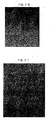
- Fig. 10 shows recorded marks on the BiGeN recording layer (Embodiment 2) in a photograph of TEM(transmission electron microscope), and Fig. 11 shows recorded marks on the SnTiN recording layer (Optical disc A) in a photograph of TEM.
- the respective recorded marks are formed of sub-micron bubbles without spreading out the guide groove during the recording.
- an elevation difference between the non-recording portion and the recording portion in the thickness direction was at most approximately 6 nm with respect to the guide groove with 27 nm depth in observation with an atomic force microscope (not shown).
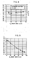
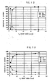
- Fig. 12 shows variations in content percentage of the non-nitride (Ge and the oxide thereof) and Ge nitride with respect to the amount of nitrogen added
- Fig. 13 shows variations in content percentage of the non-nitride (Bi and the oxide thereof) and Bi nitride with respect to the amount of nitrogen added.
- the amount of nitrogen introduced is 10 sccm or more.
- the amount of nitrogen introduced is desirably 10 to 60 sccm.
- Fig. 6 show that metal Bi remains when an introduced amount of nitrogen during deposition is 5 sccm.
- Bi exists in a mixture of metal Bi and Bi-N composition, and the percentage of nitride increases as the introduced amount of nitrogen increases during deposition.
- the introduced amount of nitrogen during deposition is 80 sccm, about 94% of Bi is nitrated. Therefore, it is preferable that 85% or more of Ge is nitrided and 94% or less of Bi is nitrided. Further, it is preferable that 85% of Ge is nitrided and 90% or less of Bi is nitrided in a case where the introduced amount of nitrogen during deposition is 60 sccm, which is required so as to enhance recording sensitivity.
- the metal component ratio in the recording layer is a wide range (the high temperature decomposable compound such as metal nitride range from 20 to 40 atm.%), which has a good characteristic.
- the high temperature decomposable compound consists of nitride, it is necessary to adjust the nitrogen flow rate so that the film is perfectly nitrided during deposition.
- the non-nitrided component is reduced in the low temperature decomposable nitride to decrease the absorption rate of the recording layer.
- the sensitivity of the recording layer become inferior and the deposition rate of film is reduced to decrease productivity of the layer. Therefore, the quantity of the added nitrogen should be adjusted as possible in a bit for the benefit of productivity.
- Fig. 14 shows a setting method for determining conditions of the reactive sputtering deposition to form a recording layer in which the high temperature decomposable compound of the recording layer consists of metal nitride.
- a sputtering target consisting of alloy including metal components to be included in such metal nitride, or of oxide thereof or of nitride thereof.
- an alloy target is provided in a chamber of the sputtering device (SS1).
- flow rates of Ar gas and nitrogen gas are decided on the basis of predetermined initial values as sputtering introducing gases (SS2).
- SS3 reactive sputtering deposition is preformed
- the deposited recording layer is analyzed in component (SS4).
- the judgment whether or not the high temperature decomposable compound is perfectly nitrided is performed (SS5).
- SS5 the judgment whether or not the high temperature decomposable compound is not perfectly nitrided
- SS2 the flow rate decision step
- SS6 the judgment whether or not the non-nitrided component of the low temperature decomposable nitride exists in the layer.
- the non-nitrided component of the low temperature decomposable nitride is insufficient then back to the flow rate decision step (SS2) to decrease the flow rate of nitrogen gas to ensure the non-nitrided component in the recording layer.
- SS7 flow rate of nitrogen gas as it is (SS7) and thus the setting of deposition conditions of the recording layer is completed.
- the determined flow rate of nitrogen gas goes forward to the step of manufacturing the recording layer.
- the foregoing setting method of deposition conditions may be used in case that materials other than metal nitride are used for the recording layer.
- the mixed recording layer can be formed at once in the reactive sputtering deposition with added nitrogen while adjusting target contents.
Landscapes
- Engineering & Computer Science (AREA)
- Manufacturing & Machinery (AREA)
- Chemical & Material Sciences (AREA)
- Inorganic Chemistry (AREA)
- Physics & Mathematics (AREA)
- Optics & Photonics (AREA)
- Optical Record Carriers And Manufacture Thereof (AREA)
- Thermal Transfer Or Thermal Recording In General (AREA)
- Manufacturing Optical Record Carriers (AREA)
Claims (19)
- Datenaufzeichnungsmedium, welches eine Aufzeichnungsschicht umfasst, die ein Material enthält mit einer Reflektivität, die sich durch Einstrahlung eines Lichtstrahls ändert und auf welcher Information aufgezeichnet ist als Reflektivitätsschwankungen, und ein Substrat zum Stützen der Aufzeichnungsschicht, dadurch gekennzeichnet, dass die Aufzeichnungsschicht besteht aus:einer inorganischen Mischung von sowohl bei niedriger Temperatur zersetzbarem Metallnitrid, welches in der Lage ist, bei einer Temperatur zwischen 100 °C und 600 °C zersetzt zu werden und einer bei hoher Temperatur zersetzbaren Verbindung einer Substanz, die ausgewählt ist aus einer Gruppe, die ein Metallnitrid umfasst, ein Metalloxid und ein Metallkarbid oder eine Mischung von zumindest zwei hiervon, welche in der Lage ist, zersetzt zu werden bei einer Temperatur höher als die vorgenannte Temperatur, undunvermeidlichen Verunreinigungen.
- Datenaufzeichnungsmedium nach Anspruch 1, wobei das bei niedriger Temperatur zersetzbare Metallnitrid bei dieser Temperatur im Bereich von 100 °C bis 600 °C zersetzt wird, aber unzureichend nitriert wird.
- Datenaufzeichnungsmedium nach Anspruch 1, wobei die Aufzeichnungsschicht ausgebildet ist durch ein reaktives Sputteringverfahren mit einer Stickstoffatmosphäre unter Verwendung eines Targets zum Sputtern, während Stickstoff eingeführt wird in die Sputteringatmosphäre und Anpassen des Stickstoffs auf solch eine Weise, dass die Aufzeichnungsschicht eine nicht nitrierte Komponente umfasst, wobei das Target besteht aus zumindest einer Legierung, einem Oxid und einem Nitrid, von denen jedes zumindest eine metallische Komponente im Metallnitrid umfasst.
- Datenaufzeichnungsmedium nach Anspruch 1, wobei die Aufzeichnungsschicht ausgebildet wird durch ein Sputteringverfahren unter Verwendung eines Targets zum Sputtern auf solch eine Weise, dass die Aufzeichnungsschicht eine nicht nitrierte Komponente umfasst, wobei das Target hergestellt ist aus einem Nitrid, welches eine Metallkomponente in dem Metallnitrid umfasst.
- Datenaufzeichnungsmedium nach Anspruch 2, wobei das bei niedriger Temperatur zersetzbare Metall ein Nitrid ist, welches zumindest ein Element von Bi, Sn, oder Fe umfasst.
- Datenaufzeichnungsmedium nach Anspruch 2, wobei die bei hoher Temperatur zersetzbare Verbindung ein Nitrid ist, welches zumindest ein Element von Ge, Ti, Si oder Al umfasst.
- Datenaufzeichnungsmedium nach Anspruch 2, wobei das bei niedriger Temperatur zersetzbare Metallnitrid ein Nitrid aus Cu ist.
- Datenaufzeichnungsmedium nach Anspruch 1, wobei das Metallnitrid ein beliebiges Element umfasst aus der Gruppe von Bi, Sn und Fe und zumindest ein Material, welches ausgewählt ist aus der Gruppe von Si, Ge, Al und Ti.
- Datenaufzeichnungsmedium nach Anspruch 1, wobei das Metallnitrid Bi und Ge enthält und das Ge nitriert ist bei 85 % oder mehr.
- Datenaufzeichnungsmedium nach Anspruch 9, wobei das Bi bei 90 % oder weniger nitriert ist.
- Datenaufzeichnungsmedium nach Anspruch 9, wobei das Bi bei 94 % oder weniger nitriert ist.
- Datenaufzeichnungsmedium nach Anspruch 1, wobei das Metallnitrid ein beliebiges Element enthält aus Bi, Sn und Fe, und zumindest ein Material ausgewählt aus Mg, Ca, Sr, Sc, Y, Zr, Hf, V, Nb, Tc, Ru, Rh W, Re, Os, Ir, Pt, Au, Ta, Ga, O und C.
- Datenaufzeichnungsmedium nach Anspruch 1, wobei das Metallnitrid zumindest ein Element aus der Gruppe von Bi, Sn und Fe enthält, und zumindest ein Material, das ausgewählt ist aus Tl, Te, In, Zn und Ag.
- Datenaufzeichnungsmedium nach Anspruch 1, wobei das Metallnitrid Cu enthält, und zumindest ein Material ausgewählt aus Si, Ge, Al, Ti, Mg, Ca, Sr, Sc, Y, Zr, Hf, V, Nb, Tc, Ru, Rh, W, Re, Os, Ir, Pt, Au, Ta, Ga, Tl, Te, In, Zn, Ag, O und C.
- Datenaufzeichnungsmedium nach einem der Ansprüche 1 bis 14, wobei es eine Schutzschicht aufweist zum Schützen der Aufzeichnungsschicht.
- Datenaufzeichnungsmedium nach einem der Ansprüche 1 bis 15, wobei es eine reflektierende Schicht aufweist auf einer Seite gegenüberliegend zu der, auf welcher der Lichtstrahl eingestrahlt wird.
- Datenaufzeichnungsmedium nach einem der Ansprüche 1 bis 16, wobei der Lichtstrahl eine Wellenlänge von 385 bis 450 nm hat.
- Verfahren zum Herstellen eines Datenaufzeichnungsmediums mit einer Aufzeichnungsschicht, welche ein Material umfasst, das eine Reflektivität hat, die bei der Einstrahlung eines Lichtstsrahls schwankt, auf welchem Information aufgezeichnet wird als Reflektionsschwankungen und ein Substrat zum Schützen der Aufzeichnungsschicht,
dadurch gekennzeichnet, dass die Aufzeichnungsschicht besteht aus:einer inorganischen Mischung aus sowohl einem bei niedriger Temperatur zersetzbarem Metallnitrid, welches in der Lage ist, zersetzt zu werden bei einer Temperatur, die von 100 °C bis 600 °C reicht, und einer bei hoher Temperatur zersetzbaren Verbindung einer Substanz, die ausgewählt ist aus einer Gruppe, die aus einem Metallnitrid besteht, einem Metalloxid und einem Metallkarbid oder einer Mischung von zumindest zwei davon, welches in der Lage ist, zersetzt zu werden bei einer Temperatur, die höher ist als die genannte Temperatur; undunvermeidliche Verunreinigungen; unddadurch gekennzeichnet, dass das Verfahren umfasst: einen Schritt zum Bilden einer Aufzeichnungsschicht zum Formen der Aufzeichnungsschicht durch ein reaktives Sputteringverfahren unter Verwendung eines Targets, welches aus einem Metall besteht, welches das Metallnitrid festlegt; und dadurch gekennzeichnet, dass ein Flussverhältnis Ar:N2 in einer Atmosphäre, die Ar und N2 enthält, in dem Aufzeichnungsformungsschritt eingestellt ist in dem Bereich zwischen 80:10 bis 10:80. - Verfahren zum Herstellen eines Datenaufzeichnungsmediums gemäß Anspruch 18, wobei das Flussverhältnis Ar:N2 eingestellt ist auf den Bereich zwischen 80:10 bis 30:60.
Applications Claiming Priority (5)
| Application Number | Priority Date | Filing Date | Title |
|---|---|---|---|
| JP2002162047 | 2002-06-03 | ||
| JP2002162047 | 2002-06-03 | ||
| JP2003024139 | 2003-01-31 | ||
| JP2003024139 | 2003-01-31 | ||
| PCT/JP2003/006439 WO2003101750A1 (fr) | 2002-06-03 | 2003-05-23 | Support d'enregistrement d'information et son procede de production |
Publications (3)
| Publication Number | Publication Date |
|---|---|
| EP1510355A1 EP1510355A1 (de) | 2005-03-02 |
| EP1510355A4 EP1510355A4 (de) | 2005-07-13 |
| EP1510355B1 true EP1510355B1 (de) | 2007-02-14 |
Family
ID=29714331
Family Applications (1)
| Application Number | Title | Priority Date | Filing Date |
|---|---|---|---|
| EP03733031A Expired - Lifetime EP1510355B1 (de) | 2002-06-03 | 2003-05-23 | Datenaufzeichnungsmedium und herstellungsverfahren dafür |
Country Status (9)
| Country | Link |
|---|---|
| US (1) | US7524612B2 (de) |
| EP (1) | EP1510355B1 (de) |
| JP (1) | JP3810076B2 (de) |
| KR (1) | KR100709931B1 (de) |
| CN (2) | CN1659041A (de) |
| AU (1) | AU2003242414A1 (de) |
| DE (1) | DE60311804T2 (de) |
| TW (1) | TWI236674B (de) |
| WO (1) | WO2003101750A1 (de) |
Families Citing this family (24)
| Publication number | Priority date | Publication date | Assignee | Title |
|---|---|---|---|---|
| JP2005044450A (ja) * | 2003-07-24 | 2005-02-17 | Tdk Corp | 光記録媒体及びその製造方法、並びに、光記録媒体に対するデータ記録方法及びデータ再生方法 |
| WO2005018947A1 (ja) * | 2003-08-21 | 2005-03-03 | Mitsubishi Kagaku Media Co., Ltd. | 記録媒体 |
| CN100351933C (zh) | 2004-04-22 | 2007-11-28 | Tdk股份有限公司 | 光记录媒体 |
| US7427431B2 (en) * | 2004-04-28 | 2008-09-23 | Sony Corporation | Write once optical recording medium |
| JP2006281751A (ja) * | 2004-04-28 | 2006-10-19 | Sony Corp | 追記型光記録媒体 |
| US7235501B2 (en) | 2004-12-13 | 2007-06-26 | Micron Technology, Inc. | Lanthanum hafnium oxide dielectrics |
| JP2006018986A (ja) * | 2005-01-20 | 2006-01-19 | Pioneer Electronic Corp | 光記録媒体及びその製造方法 |
| US7803445B2 (en) | 2005-02-23 | 2010-09-28 | Pioneer Corporation | Optical recording medium |
| US7410910B2 (en) | 2005-08-31 | 2008-08-12 | Micron Technology, Inc. | Lanthanum aluminum oxynitride dielectric films |
| US7972974B2 (en) | 2006-01-10 | 2011-07-05 | Micron Technology, Inc. | Gallium lanthanide oxide films |
| JP4560495B2 (ja) * | 2006-06-16 | 2010-10-13 | 三菱化学メディア株式会社 | 記録媒体 |
| US7605030B2 (en) | 2006-08-31 | 2009-10-20 | Micron Technology, Inc. | Hafnium tantalum oxynitride high-k dielectric and metal gates |
| US7432548B2 (en) | 2006-08-31 | 2008-10-07 | Micron Technology, Inc. | Silicon lanthanide oxynitride films |
| US7563730B2 (en) | 2006-08-31 | 2009-07-21 | Micron Technology, Inc. | Hafnium lanthanide oxynitride films |
| US7776765B2 (en) | 2006-08-31 | 2010-08-17 | Micron Technology, Inc. | Tantalum silicon oxynitride high-k dielectrics and metal gates |
| US7544604B2 (en) | 2006-08-31 | 2009-06-09 | Micron Technology, Inc. | Tantalum lanthanide oxynitride films |
| US7759747B2 (en) | 2006-08-31 | 2010-07-20 | Micron Technology, Inc. | Tantalum aluminum oxynitride high-κ dielectric |
| US8124211B2 (en) | 2007-03-28 | 2012-02-28 | Ricoh Company, Ltd. | Optical recording medium, sputtering target, and method for manufacturing the same |
| JP4577581B2 (ja) * | 2007-08-30 | 2010-11-10 | ソニー株式会社 | 光情報記録媒体 |
| JP2009143184A (ja) * | 2007-12-17 | 2009-07-02 | Kobe Steel Ltd | 光情報記録媒体用記録層および光情報記録媒体 |
| WO2009104239A1 (ja) * | 2008-02-18 | 2009-08-27 | 株式会社 東芝 | 不揮発性記憶装置及びその製造方法 |
| JP4969624B2 (ja) | 2008-11-12 | 2012-07-04 | 株式会社神戸製鋼所 | 光情報記録媒体 |
| JP5399836B2 (ja) | 2009-09-18 | 2014-01-29 | 株式会社神戸製鋼所 | 光情報記録媒体用記録層、光情報記録媒体およびスパッタリングターゲット |
| KR20120057629A (ko) | 2009-09-18 | 2012-06-05 | 소니 주식회사 | 광 정보 기록 매체용 기록층, 광 정보 기록 매체 및 스퍼터링 타깃 |
Family Cites Families (30)
| Publication number | Priority date | Publication date | Assignee | Title |
|---|---|---|---|---|
| US4188214A (en) * | 1975-08-11 | 1980-02-12 | Fuji Photo Film Co., Ltd. | Recording material |
| US4470053A (en) * | 1981-02-13 | 1984-09-04 | Minnesota Mining And Manufacturing Company | Protuberant optical recording medium |
| JPS6134741A (ja) * | 1984-07-09 | 1986-02-19 | アメリカン テレフォン アンド テレグラフ カムパニー | 情報蓄積用媒体 |
| JPS6211685A (ja) * | 1985-07-10 | 1987-01-20 | Mitsubishi Chem Ind Ltd | 光学的記録媒体 |
| JPS62114133A (ja) * | 1985-11-13 | 1987-05-25 | Hitachi Maxell Ltd | 追記型情報記録用デイスク |
| US4839208A (en) | 1986-04-30 | 1989-06-13 | Nec Corporation | Optical information recording medium |
| JPS6363153A (ja) * | 1986-09-03 | 1988-03-19 | Nec Corp | 光記録媒体の製造方法 |
| JPS63299984A (ja) * | 1987-05-30 | 1988-12-07 | Kuraray Co Ltd | 光記録媒体及びその製造法 |
| US5034255A (en) * | 1988-10-28 | 1991-07-23 | Mitsui Petrochemical Industries, Ltd. | Optical recording medium and method of its production |
| JPH02147392A (ja) * | 1988-11-30 | 1990-06-06 | Toshiba Corp | 情報記録媒体 |
| JP2918894B2 (ja) * | 1988-12-20 | 1999-07-12 | 明 田崎 | 光記録媒体及びその製造方法 |
| JPH02215587A (ja) * | 1989-02-17 | 1990-08-28 | Toshiba Corp | 光情報記録媒体 |
| JPH02277689A (ja) | 1989-04-20 | 1990-11-14 | Toshiba Corp | 光情報記録媒体 |
| JPH03153389A (ja) * | 1989-11-09 | 1991-07-01 | Kuraray Co Ltd | 光記録媒体 |
| JP2836227B2 (ja) * | 1990-09-11 | 1998-12-14 | 松下電器産業株式会社 | 光記録媒体とその製造方法、及び光記録媒体用スパッタリングターゲットとその製造方法 |
| US5232566A (en) * | 1991-05-14 | 1993-08-03 | International Business Machines Corporation | Underlayer doping in thin film magnetic recording media |
| JP3088168B2 (ja) * | 1991-12-13 | 2000-09-18 | ティーディーケイ株式会社 | 光記録媒体およびその製造方法 |
| JPH05212967A (ja) | 1992-02-04 | 1993-08-24 | Dainippon Printing Co Ltd | 光記録媒体及びその製造方法 |
| US5334433A (en) | 1992-12-28 | 1994-08-02 | Tdk Corporation | Optical recording medium |
| JP3026327B2 (ja) * | 1996-07-25 | 2000-03-27 | インダストリアル テクノロジー リサーチ インスティチュート | 追記型光ディスクおよび光記録媒体 |
| JPH10222871A (ja) * | 1997-02-06 | 1998-08-21 | Denso Corp | 光情報記録媒体およびその製造方法 |
| JPH10329424A (ja) * | 1997-06-04 | 1998-12-15 | Denso Corp | 光情報記録媒体およびその製造方法 |
| JP3570169B2 (ja) * | 1997-08-22 | 2004-09-29 | 松下電器産業株式会社 | 光学情報記録媒体 |
| JPH11138996A (ja) * | 1997-11-12 | 1999-05-25 | Toyota Central Res & Dev Lab Inc | 記憶部材 |
| JP3697896B2 (ja) * | 1998-01-23 | 2005-09-21 | 株式会社デンソー | 光情報記録媒体およびその製造方法 |
| JPH11232692A (ja) * | 1998-02-10 | 1999-08-27 | Sony Corp | 光記録媒体及びその製造方法 |
| US5972458A (en) * | 1998-04-01 | 1999-10-26 | Eastman Kodak Company | Optical recording element with an interfacial layer between the recording layer and the reflecting layer |
| WO2000004536A1 (en) * | 1998-07-14 | 2000-01-27 | Kabushiki Kaisha Toyota Chuo Kenkyusho | Storage member |
| TW484126B (en) * | 1999-03-26 | 2002-04-21 | Matsushita Electric Industrial Co Ltd | Manufacturing and recording regeneration method for information record medium |
| WO2005018947A1 (ja) * | 2003-08-21 | 2005-03-03 | Mitsubishi Kagaku Media Co., Ltd. | 記録媒体 |
-
2003
- 2003-05-23 EP EP03733031A patent/EP1510355B1/de not_active Expired - Lifetime
- 2003-05-23 CN CN038127903A patent/CN1659041A/zh active Pending
- 2003-05-23 JP JP2004509072A patent/JP3810076B2/ja not_active Expired - Lifetime
- 2003-05-23 CN CN2008101273000A patent/CN101320576B/zh not_active Expired - Lifetime
- 2003-05-23 AU AU2003242414A patent/AU2003242414A1/en not_active Abandoned
- 2003-05-23 US US10/516,244 patent/US7524612B2/en not_active Expired - Lifetime
- 2003-05-23 DE DE60311804T patent/DE60311804T2/de not_active Expired - Lifetime
- 2003-05-23 KR KR1020047019759A patent/KR100709931B1/ko not_active Expired - Lifetime
- 2003-05-23 WO PCT/JP2003/006439 patent/WO2003101750A1/ja not_active Ceased
- 2003-05-30 TW TW092114819A patent/TWI236674B/zh not_active IP Right Cessation
Also Published As
| Publication number | Publication date |
|---|---|
| TWI236674B (en) | 2005-07-21 |
| DE60311804D1 (de) | 2007-03-29 |
| EP1510355A1 (de) | 2005-03-02 |
| DE60311804T2 (de) | 2007-10-31 |
| CN101320576B (zh) | 2012-07-11 |
| KR100709931B1 (ko) | 2007-04-24 |
| JP3810076B2 (ja) | 2006-08-16 |
| JPWO2003101750A1 (ja) | 2005-09-29 |
| TW200402711A (en) | 2004-02-16 |
| CN1659041A (zh) | 2005-08-24 |
| HK1072037A1 (en) | 2005-08-12 |
| KR20050009734A (ko) | 2005-01-25 |
| WO2003101750A1 (fr) | 2003-12-11 |
| US7524612B2 (en) | 2009-04-28 |
| EP1510355A4 (de) | 2005-07-13 |
| CN101320576A (zh) | 2008-12-10 |
| US20050233247A1 (en) | 2005-10-20 |
| AU2003242414A1 (en) | 2003-12-19 |
Similar Documents
| Publication | Publication Date | Title |
|---|---|---|
| EP1510355B1 (de) | Datenaufzeichnungsmedium und herstellungsverfahren dafür | |
| EP0978831B1 (de) | Optisches Aufzeichnungsmedium und Verfahren zu seiner Herstellung, Verfahren zur Informationsaufzeichnung und -wiedergabe darauf, und Aufzeichnungs-/Wiedergabegerät | |
| EP1437724B1 (de) | Optischer Aufzeichnungsträger | |
| EP1657071B1 (de) | Aufzeichnungsmedium | |
| EP1394786B1 (de) | Optisches Aufzeichnungsmedium und Verfahren zum Aufzeichnen optischer Daten auf demselben | |
| KR100685061B1 (ko) | 광기록매체 및 이를 제조하기 위한 방법, 및 광기록매체상에 데이터를 기록하기 위한 방법 및 광기록매체로부터데이터를 재생하는 방법 | |
| EP1414029A2 (de) | Optisches Aufzeichnungsmedium und Verfahren zu dessen Herstellung | |
| US6352753B2 (en) | Optical recording medium | |
| EP1345218B1 (de) | Medium für optische Datenspeicherung sowie dessen Herstellungsverfahren, und Aufzeichnungs- sowie Reproduktionsverfahren unter Benutzung dieses Mediums | |
| EP1548721B1 (de) | Optisches aufzeichnungsmedium | |
| EP1548722B1 (de) | Optisches informationsaufzeichnungsmedium und verfahren zu seiner herstellung | |
| EP1426940B1 (de) | Optisches informationsaufzeichnungmedium und dieses verwendendes aufzeichnungsverfahren | |
| HK1072037B (en) | Information recording medium and process for producing the same | |
| EP1710088A1 (de) | Optischer aufzeichnungs-datenträger und herstellungsverfahren dafür | |
| JP3889028B2 (ja) | 情報記録媒体 | |
| KR20110086668A (ko) | 정보 기록 매체, 기록 장치, 재생 장치 및 재생 방법 | |
| JP2006182030A (ja) | 情報記録媒体 | |
| JP3608934B2 (ja) | 光記録媒体及び光記録媒体用保護膜 | |
| JP2001167475A (ja) | 光記録媒体 | |
| EP1524656B1 (de) | Medium zur optischen Datenspeicherung und Verfahren zu dessen Herstellung | |
| JP4232159B2 (ja) | 光記録媒体 | |
| US20060165944A1 (en) | Optical recording medium | |
| JPH11314455A (ja) | 光記録媒体 | |
| JP2005203072A (ja) | 光記録媒体 | |
| JPH11250499A (ja) | 光記録媒体 |
Legal Events
| Date | Code | Title | Description |
|---|---|---|---|
| PUAI | Public reference made under article 153(3) epc to a published international application that has entered the european phase |
Free format text: ORIGINAL CODE: 0009012 |
|
| 17P | Request for examination filed |
Effective date: 20041125 |
|
| AK | Designated contracting states |
Kind code of ref document: A1 Designated state(s): AT BE BG CH CY CZ DE DK EE ES FI FR GB GR HU IE IT LI LU MC NL PT RO SE SI SK TR |
|
| AX | Request for extension of the european patent |
Extension state: AL LT LV MK |
|
| A4 | Supplementary search report drawn up and despatched |
Effective date: 20050531 |
|
| REG | Reference to a national code |
Ref country code: HK Ref legal event code: DE Ref document number: 1072037 Country of ref document: HK |
|
| DAX | Request for extension of the european patent (deleted) | ||
| RBV | Designated contracting states (corrected) |
Designated state(s): DE FR GB |
|
| GRAP | Despatch of communication of intention to grant a patent |
Free format text: ORIGINAL CODE: EPIDOSNIGR1 |
|
| GRAS | Grant fee paid |
Free format text: ORIGINAL CODE: EPIDOSNIGR3 |
|
| GRAA | (expected) grant |
Free format text: ORIGINAL CODE: 0009210 |
|
| AK | Designated contracting states |
Kind code of ref document: B1 Designated state(s): DE FR GB |
|
| REG | Reference to a national code |
Ref country code: GB Ref legal event code: FG4D |
|
| REF | Corresponds to: |
Ref document number: 60311804 Country of ref document: DE Date of ref document: 20070329 Kind code of ref document: P |
|
| REG | Reference to a national code |
Ref country code: GB Ref legal event code: 746 Effective date: 20070321 |
|
| REG | Reference to a national code |
Ref country code: HK Ref legal event code: GR Ref document number: 1072037 Country of ref document: HK |
|
| ET | Fr: translation filed | ||
| PLBE | No opposition filed within time limit |
Free format text: ORIGINAL CODE: 0009261 |
|
| STAA | Information on the status of an ep patent application or granted ep patent |
Free format text: STATUS: NO OPPOSITION FILED WITHIN TIME LIMIT |
|
| 26N | No opposition filed |
Effective date: 20071115 |
|
| REG | Reference to a national code |
Ref country code: FR Ref legal event code: PLFP Year of fee payment: 14 |
|
| REG | Reference to a national code |
Ref country code: FR Ref legal event code: PLFP Year of fee payment: 15 |
|
| REG | Reference to a national code |
Ref country code: FR Ref legal event code: PLFP Year of fee payment: 16 |
|
| PGFP | Annual fee paid to national office [announced via postgrant information from national office to epo] |
Ref country code: GB Payment date: 20220401 Year of fee payment: 20 Ref country code: FR Payment date: 20220408 Year of fee payment: 20 Ref country code: DE Payment date: 20220329 Year of fee payment: 20 |
|
| REG | Reference to a national code |
Ref country code: DE Ref legal event code: R071 Ref document number: 60311804 Country of ref document: DE |
|
| REG | Reference to a national code |
Ref country code: GB Ref legal event code: PE20 Expiry date: 20230522 |
|
| PG25 | Lapsed in a contracting state [announced via postgrant information from national office to epo] |
Ref country code: GB Free format text: LAPSE BECAUSE OF EXPIRATION OF PROTECTION Effective date: 20230522 |