EP1500719B1 - Méthode pour fabriquer des circuits imprimés en cuivre - Google Patents
Méthode pour fabriquer des circuits imprimés en cuivre Download PDFInfo
- Publication number
- EP1500719B1 EP1500719B1 EP04017218A EP04017218A EP1500719B1 EP 1500719 B1 EP1500719 B1 EP 1500719B1 EP 04017218 A EP04017218 A EP 04017218A EP 04017218 A EP04017218 A EP 04017218A EP 1500719 B1 EP1500719 B1 EP 1500719B1
- Authority
- EP
- European Patent Office
- Prior art keywords
- liter
- etchant
- copper
- solution
- producing
- Prior art date
- Legal status (The legal status is an assumption and is not a legal conclusion. Google has not performed a legal analysis and makes no representation as to the accuracy of the status listed.)
- Active
Links
- RYGMFSIKBFXOCR-UHFFFAOYSA-N Copper Chemical compound [Cu] RYGMFSIKBFXOCR-UHFFFAOYSA-N 0.000 title claims description 35
- 239000010949 copper Substances 0.000 title claims description 32
- 229910052802 copper Inorganic materials 0.000 title claims description 32
- 238000004519 manufacturing process Methods 0.000 title claims description 14
- VEXZGXHMUGYJMC-UHFFFAOYSA-N Hydrochloric acid Chemical compound Cl VEXZGXHMUGYJMC-UHFFFAOYSA-N 0.000 claims description 47
- 238000005530 etching Methods 0.000 claims description 35
- ORTQZVOHEJQUHG-UHFFFAOYSA-L copper(II) chloride Chemical compound Cl[Cu]Cl ORTQZVOHEJQUHG-UHFFFAOYSA-L 0.000 claims description 33
- 239000000243 solution Substances 0.000 claims description 31
- JPVYNHNXODAKFH-UHFFFAOYSA-N Cu2+ Chemical compound [Cu+2] JPVYNHNXODAKFH-UHFFFAOYSA-N 0.000 claims description 23
- 238000004140 cleaning Methods 0.000 claims description 19
- 229960003280 cupric chloride Drugs 0.000 claims description 15
- 229910001431 copper ion Inorganic materials 0.000 claims description 13
- 150000001875 compounds Chemical class 0.000 claims description 12
- 229910000881 Cu alloy Inorganic materials 0.000 claims description 11
- LYCAIKOWRPUZTN-UHFFFAOYSA-N Ethylene glycol Chemical compound OCCO LYCAIKOWRPUZTN-UHFFFAOYSA-N 0.000 claims description 11
- 239000012530 fluid Substances 0.000 claims description 10
- 150000003536 tetrazoles Chemical class 0.000 claims description 10
- 239000004094 surface-active agent Substances 0.000 claims description 8
- MTHSVFCYNBDYFN-UHFFFAOYSA-N diethylene glycol Chemical compound OCCOCCO MTHSVFCYNBDYFN-UHFFFAOYSA-N 0.000 claims description 7
- 239000007864 aqueous solution Substances 0.000 claims description 6
- 239000000126 substance Substances 0.000 claims description 6
- 239000002253 acid Substances 0.000 claims description 5
- 125000002091 cationic group Chemical group 0.000 claims description 4
- WGCNASOHLSPBMP-UHFFFAOYSA-N hydroxyacetaldehyde Natural products OCC=O WGCNASOHLSPBMP-UHFFFAOYSA-N 0.000 claims description 4
- 238000000034 method Methods 0.000 description 16
- XLYOFNOQVPJJNP-UHFFFAOYSA-N water Substances O XLYOFNOQVPJJNP-UHFFFAOYSA-N 0.000 description 13
- -1 azole compound Chemical class 0.000 description 11
- 239000000463 material Substances 0.000 description 8
- KAESVJOAVNADME-UHFFFAOYSA-N 1H-pyrrole Natural products C=1C=CNC=1 KAESVJOAVNADME-UHFFFAOYSA-N 0.000 description 5
- ULRPISSMEBPJLN-UHFFFAOYSA-N 2h-tetrazol-5-amine Chemical compound NC1=NN=NN1 ULRPISSMEBPJLN-UHFFFAOYSA-N 0.000 description 5
- 239000010410 layer Substances 0.000 description 5
- 238000005507 spraying Methods 0.000 description 5
- KJUGUADJHNHALS-UHFFFAOYSA-N 1H-tetrazole Substances C=1N=NNN=1 KJUGUADJHNHALS-UHFFFAOYSA-N 0.000 description 4
- MARUHZGHZWCEQU-UHFFFAOYSA-N 5-phenyl-2h-tetrazole Chemical compound C1=CC=CC=C1C1=NNN=N1 MARUHZGHZWCEQU-UHFFFAOYSA-N 0.000 description 4
- MHAJPDPJQMAIIY-UHFFFAOYSA-N Hydrogen peroxide Chemical compound OO MHAJPDPJQMAIIY-UHFFFAOYSA-N 0.000 description 4
- PXHVJJICTQNCMI-UHFFFAOYSA-N Nickel Chemical compound [Ni] PXHVJJICTQNCMI-UHFFFAOYSA-N 0.000 description 4
- 125000005842 heteroatom Chemical group 0.000 description 4
- 125000004433 nitrogen atom Chemical group N* 0.000 description 4
- 239000000758 substrate Substances 0.000 description 4
- UHGULLIUJBCTEF-UHFFFAOYSA-N 2-aminobenzothiazole Chemical compound C1=CC=C2SC(N)=NC2=C1 UHGULLIUJBCTEF-UHFFFAOYSA-N 0.000 description 3
- XZGLNCKSNVGDNX-UHFFFAOYSA-N 5-methyl-2h-tetrazole Chemical compound CC=1N=NNN=1 XZGLNCKSNVGDNX-UHFFFAOYSA-N 0.000 description 3
- 239000004593 Epoxy Substances 0.000 description 3
- LFQSCWFLJHTTHZ-UHFFFAOYSA-N Ethanol Chemical compound CCO LFQSCWFLJHTTHZ-UHFFFAOYSA-N 0.000 description 3
- KFZMGEQAYNKOFK-UHFFFAOYSA-N Isopropanol Chemical compound CC(C)O KFZMGEQAYNKOFK-UHFFFAOYSA-N 0.000 description 3
- OKKJLVBELUTLKV-UHFFFAOYSA-N Methanol Chemical compound OC OKKJLVBELUTLKV-UHFFFAOYSA-N 0.000 description 3
- ZMXDDKWLCZADIW-UHFFFAOYSA-N N,N-Dimethylformamide Chemical compound CN(C)C=O ZMXDDKWLCZADIW-UHFFFAOYSA-N 0.000 description 3
- DNIAPMSPPWPWGF-UHFFFAOYSA-N Propylene glycol Chemical compound CC(O)CO DNIAPMSPPWPWGF-UHFFFAOYSA-N 0.000 description 3
- HEMHJVSKTPXQMS-UHFFFAOYSA-M Sodium hydroxide Chemical compound [OH-].[Na+] HEMHJVSKTPXQMS-UHFFFAOYSA-M 0.000 description 3
- 239000000654 additive Substances 0.000 description 3
- 230000000052 comparative effect Effects 0.000 description 3
- 239000011889 copper foil Substances 0.000 description 3
- 239000011521 glass Substances 0.000 description 3
- 239000000203 mixture Substances 0.000 description 3
- BDERNNFJNOPAEC-UHFFFAOYSA-N propan-1-ol Chemical compound CCCO BDERNNFJNOPAEC-UHFFFAOYSA-N 0.000 description 3
- 239000007921 spray Substances 0.000 description 3
- 238000004506 ultrasonic cleaning Methods 0.000 description 3
- ARXJGSRGQADJSQ-UHFFFAOYSA-N 1-methoxypropan-2-ol Chemical compound COCC(C)O ARXJGSRGQADJSQ-UHFFFAOYSA-N 0.000 description 2
- MFKRHJVUCZRDTF-UHFFFAOYSA-N 3-methoxy-3-methylbutan-1-ol Chemical compound COC(C)(C)CCO MFKRHJVUCZRDTF-UHFFFAOYSA-N 0.000 description 2
- QGZKDVFQNNGYKY-UHFFFAOYSA-N Ammonia Chemical compound N QGZKDVFQNNGYKY-UHFFFAOYSA-N 0.000 description 2
- IAZDPXIOMUYVGZ-UHFFFAOYSA-N Dimethylsulphoxide Chemical compound CS(C)=O IAZDPXIOMUYVGZ-UHFFFAOYSA-N 0.000 description 2
- LRHPLDYGYMQRHN-UHFFFAOYSA-N N-Butanol Chemical compound CCCCO LRHPLDYGYMQRHN-UHFFFAOYSA-N 0.000 description 2
- 229920003171 Poly (ethylene oxide) Polymers 0.000 description 2
- 239000002202 Polyethylene glycol Substances 0.000 description 2
- QAOWNCQODCNURD-UHFFFAOYSA-N Sulfuric acid Chemical compound OS(O)(=O)=O QAOWNCQODCNURD-UHFFFAOYSA-N 0.000 description 2
- 150000005215 alkyl ethers Chemical class 0.000 description 2
- 229960000686 benzalkonium chloride Drugs 0.000 description 2
- CADWTSSKOVRVJC-UHFFFAOYSA-N benzyl(dimethyl)azanium;chloride Chemical compound [Cl-].C[NH+](C)CC1=CC=CC=C1 CADWTSSKOVRVJC-UHFFFAOYSA-N 0.000 description 2
- 239000000919 ceramic Substances 0.000 description 2
- 239000003822 epoxy resin Substances 0.000 description 2
- 239000004744 fabric Substances 0.000 description 2
- KWIUHFFTVRNATP-UHFFFAOYSA-N glycine betaine Chemical compound C[N+](C)(C)CC([O-])=O KWIUHFFTVRNATP-UHFFFAOYSA-N 0.000 description 2
- 150000002500 ions Chemical class 0.000 description 2
- 239000002184 metal Substances 0.000 description 2
- 229910052751 metal Inorganic materials 0.000 description 2
- 239000011259 mixed solution Substances 0.000 description 2
- 229910052759 nickel Inorganic materials 0.000 description 2
- 150000007524 organic acids Chemical class 0.000 description 2
- 230000001590 oxidative effect Effects 0.000 description 2
- 238000007747 plating Methods 0.000 description 2
- 229920000647 polyepoxide Polymers 0.000 description 2
- 229920001223 polyethylene glycol Polymers 0.000 description 2
- 229920001451 polypropylene glycol Polymers 0.000 description 2
- 239000004065 semiconductor Substances 0.000 description 2
- 239000002904 solvent Substances 0.000 description 2
- 230000001629 suppression Effects 0.000 description 2
- CYSGHNMQYZDMIA-UHFFFAOYSA-N 1,3-Dimethyl-2-imidazolidinon Chemical compound CN1CCN(C)C1=O CYSGHNMQYZDMIA-UHFFFAOYSA-N 0.000 description 1
- GGZHVNZHFYCSEV-UHFFFAOYSA-N 1-Phenyl-5-mercaptotetrazole Chemical compound SC1=NN=NN1C1=CC=CC=C1 GGZHVNZHFYCSEV-UHFFFAOYSA-N 0.000 description 1
- UFYPTOJTJONMJG-UHFFFAOYSA-N 1-cyclohexyl-2h-tetrazole-5-thione Chemical compound S=C1N=NNN1C1CCCCC1 UFYPTOJTJONMJG-UHFFFAOYSA-N 0.000 description 1
- JAAIPIWKKXCNOC-UHFFFAOYSA-N 1h-tetrazol-1-ium-5-thiolate Chemical compound SC1=NN=NN1 JAAIPIWKKXCNOC-UHFFFAOYSA-N 0.000 description 1
- OAYXUHPQHDHDDZ-UHFFFAOYSA-N 2-(2-butoxyethoxy)ethanol Chemical compound CCCCOCCOCCO OAYXUHPQHDHDDZ-UHFFFAOYSA-N 0.000 description 1
- CUDYYMUUJHLCGZ-UHFFFAOYSA-N 2-(2-methoxypropoxy)propan-1-ol Chemical compound COC(C)COC(C)CO CUDYYMUUJHLCGZ-UHFFFAOYSA-N 0.000 description 1
- XPALGXXLALUMLE-UHFFFAOYSA-N 2-(dimethylamino)tetradecanoic acid Chemical compound CCCCCCCCCCCCC(N(C)C)C(O)=O XPALGXXLALUMLE-UHFFFAOYSA-N 0.000 description 1
- HZAXFHJVJLSVMW-UHFFFAOYSA-N 2-Aminoethan-1-ol Chemical compound NCCO HZAXFHJVJLSVMW-UHFFFAOYSA-N 0.000 description 1
- POAOYUHQDCAZBD-UHFFFAOYSA-N 2-butoxyethanol Chemical compound CCCCOCCO POAOYUHQDCAZBD-UHFFFAOYSA-N 0.000 description 1
- UDWODRKDBDYBRS-UHFFFAOYSA-N 2-methyl-2-(octadecylamino)propanoic acid Chemical compound CCCCCCCCCCCCCCCCCCNC(C)(C)C(O)=O UDWODRKDBDYBRS-UHFFFAOYSA-N 0.000 description 1
- QCDWFXQBSFUVSP-UHFFFAOYSA-N 2-phenoxyethanol Chemical compound OCCOC1=CC=CC=C1 QCDWFXQBSFUVSP-UHFFFAOYSA-N 0.000 description 1
- QCAHUFWKIQLBNB-UHFFFAOYSA-N 3-(3-methoxypropoxy)propan-1-ol Chemical compound COCCCOCCCO QCAHUFWKIQLBNB-UHFFFAOYSA-N 0.000 description 1
- KXDHJXZQYSOELW-UHFFFAOYSA-N Carbamic acid Chemical compound NC(O)=O KXDHJXZQYSOELW-UHFFFAOYSA-N 0.000 description 1
- VEXZGXHMUGYJMC-UHFFFAOYSA-M Chloride anion Chemical compound [Cl-] VEXZGXHMUGYJMC-UHFFFAOYSA-M 0.000 description 1
- 239000005749 Copper compound Substances 0.000 description 1
- JJLJMEJHUUYSSY-UHFFFAOYSA-L Copper hydroxide Chemical compound [OH-].[OH-].[Cu+2] JJLJMEJHUUYSSY-UHFFFAOYSA-L 0.000 description 1
- 239000005750 Copper hydroxide Substances 0.000 description 1
- QPLDLSVMHZLSFG-UHFFFAOYSA-N Copper oxide Chemical compound [Cu]=O QPLDLSVMHZLSFG-UHFFFAOYSA-N 0.000 description 1
- 239000005751 Copper oxide Substances 0.000 description 1
- 229910021591 Copper(I) chloride Inorganic materials 0.000 description 1
- 229910021578 Iron(III) chloride Inorganic materials 0.000 description 1
- SECXISVLQFMRJM-UHFFFAOYSA-N N-Methylpyrrolidone Chemical compound CN1CCCC1=O SECXISVLQFMRJM-UHFFFAOYSA-N 0.000 description 1
- ISWSIDIOOBJBQZ-UHFFFAOYSA-N Phenol Chemical compound OC1=CC=CC=C1 ISWSIDIOOBJBQZ-UHFFFAOYSA-N 0.000 description 1
- 230000002378 acidificating effect Effects 0.000 description 1
- 150000001298 alcohols Chemical class 0.000 description 1
- 125000005211 alkyl trimethyl ammonium group Chemical group 0.000 description 1
- 229910021529 ammonia Inorganic materials 0.000 description 1
- 150000001450 anions Chemical class 0.000 description 1
- 239000004760 aramid Substances 0.000 description 1
- 229920006231 aramid fiber Polymers 0.000 description 1
- 229920003235 aromatic polyamide Polymers 0.000 description 1
- QRUDEWIWKLJBPS-UHFFFAOYSA-N benzotriazole Chemical compound C1=CC=C2N[N][N]C2=C1 QRUDEWIWKLJBPS-UHFFFAOYSA-N 0.000 description 1
- 239000012964 benzotriazole Substances 0.000 description 1
- 230000015572 biosynthetic process Effects 0.000 description 1
- ODWXUNBKCRECNW-UHFFFAOYSA-M bromocopper(1+) Chemical compound Br[Cu+] ODWXUNBKCRECNW-UHFFFAOYSA-M 0.000 description 1
- 230000005587 bubbling Effects 0.000 description 1
- 238000006243 chemical reaction Methods 0.000 description 1
- 150000001880 copper compounds Chemical class 0.000 description 1
- 229910001956 copper hydroxide Inorganic materials 0.000 description 1
- 229910000431 copper oxide Inorganic materials 0.000 description 1
- 229910000365 copper sulfate Inorganic materials 0.000 description 1
- OXBLHERUFWYNTN-UHFFFAOYSA-M copper(I) chloride Chemical compound [Cu]Cl OXBLHERUFWYNTN-UHFFFAOYSA-M 0.000 description 1
- ARUVKPQLZAKDPS-UHFFFAOYSA-L copper(II) sulfate Chemical compound [Cu+2].[O-][S+2]([O-])([O-])[O-] ARUVKPQLZAKDPS-UHFFFAOYSA-L 0.000 description 1
- 239000013078 crystal Substances 0.000 description 1
- 229940045803 cuprous chloride Drugs 0.000 description 1
- 230000008021 deposition Effects 0.000 description 1
- 235000014113 dietary fatty acids Nutrition 0.000 description 1
- 125000003438 dodecyl group Chemical group [H]C([H])([H])C([H])([H])C([H])([H])C([H])([H])C([H])([H])C([H])([H])C([H])([H])C([H])([H])C([H])([H])C([H])([H])C([H])([H])C([H])([H])* 0.000 description 1
- SYELZBGXAIXKHU-UHFFFAOYSA-N dodecyldimethylamine N-oxide Chemical compound CCCCCCCCCCCC[N+](C)(C)[O-] SYELZBGXAIXKHU-UHFFFAOYSA-N 0.000 description 1
- 230000000694 effects Effects 0.000 description 1
- 239000000194 fatty acid Substances 0.000 description 1
- 229930195729 fatty acid Natural products 0.000 description 1
- 239000003365 glass fiber Substances 0.000 description 1
- 239000010931 gold Substances 0.000 description 1
- 229910052737 gold Inorganic materials 0.000 description 1
- 230000005484 gravity Effects 0.000 description 1
- 229910052736 halogen Inorganic materials 0.000 description 1
- 238000007654 immersion Methods 0.000 description 1
- 239000012535 impurity Substances 0.000 description 1
- FBAFATDZDUQKNH-UHFFFAOYSA-M iron chloride Chemical compound [Cl-].[Fe] FBAFATDZDUQKNH-UHFFFAOYSA-M 0.000 description 1
- RBTARNINKXHZNM-UHFFFAOYSA-K iron trichloride Chemical compound Cl[Fe](Cl)Cl RBTARNINKXHZNM-UHFFFAOYSA-K 0.000 description 1
- 239000007788 liquid Substances 0.000 description 1
- 150000007522 mineralic acids Chemical class 0.000 description 1
- 239000007800 oxidant agent Substances 0.000 description 1
- 230000033116 oxidation-reduction process Effects 0.000 description 1
- 239000005011 phenolic resin Substances 0.000 description 1
- 229960005323 phenoxyethanol Drugs 0.000 description 1
- 238000001259 photo etching Methods 0.000 description 1
- 239000004033 plastic Substances 0.000 description 1
- 229920003023 plastic Polymers 0.000 description 1
- 229920001515 polyalkylene glycol Polymers 0.000 description 1
- 229920000768 polyamine Polymers 0.000 description 1
- 229920001721 polyimide Polymers 0.000 description 1
- 229920000642 polymer Polymers 0.000 description 1
- 150000003242 quaternary ammonium salts Chemical class 0.000 description 1
- 238000010405 reoxidation reaction Methods 0.000 description 1
- 239000011347 resin Substances 0.000 description 1
- 229920005989 resin Polymers 0.000 description 1
- 239000002356 single layer Substances 0.000 description 1
- 229910000679 solder Inorganic materials 0.000 description 1
- 150000003462 sulfoxides Chemical class 0.000 description 1
- 238000004448 titration Methods 0.000 description 1
- 229910021642 ultra pure water Inorganic materials 0.000 description 1
- 239000012498 ultrapure water Substances 0.000 description 1
Images
Classifications
-
- C—CHEMISTRY; METALLURGY
- C23—COATING METALLIC MATERIAL; COATING MATERIAL WITH METALLIC MATERIAL; CHEMICAL SURFACE TREATMENT; DIFFUSION TREATMENT OF METALLIC MATERIAL; COATING BY VACUUM EVAPORATION, BY SPUTTERING, BY ION IMPLANTATION OR BY CHEMICAL VAPOUR DEPOSITION, IN GENERAL; INHIBITING CORROSION OF METALLIC MATERIAL OR INCRUSTATION IN GENERAL
- C23F—NON-MECHANICAL REMOVAL OF METALLIC MATERIAL FROM SURFACE; INHIBITING CORROSION OF METALLIC MATERIAL OR INCRUSTATION IN GENERAL; MULTI-STEP PROCESSES FOR SURFACE TREATMENT OF METALLIC MATERIAL INVOLVING AT LEAST ONE PROCESS PROVIDED FOR IN CLASS C23 AND AT LEAST ONE PROCESS COVERED BY SUBCLASS C21D OR C22F OR CLASS C25
- C23F1/00—Etching metallic material by chemical means
- C23F1/10—Etching compositions
- C23F1/14—Aqueous compositions
- C23F1/16—Acidic compositions
- C23F1/18—Acidic compositions for etching copper or alloys thereof
-
- C—CHEMISTRY; METALLURGY
- C09—DYES; PAINTS; POLISHES; NATURAL RESINS; ADHESIVES; COMPOSITIONS NOT OTHERWISE PROVIDED FOR; APPLICATIONS OF MATERIALS NOT OTHERWISE PROVIDED FOR
- C09K—MATERIALS FOR MISCELLANEOUS APPLICATIONS, NOT PROVIDED FOR ELSEWHERE
- C09K13/00—Etching, surface-brightening or pickling compositions
- C09K13/04—Etching, surface-brightening or pickling compositions containing an inorganic acid
-
- C—CHEMISTRY; METALLURGY
- C23—COATING METALLIC MATERIAL; COATING MATERIAL WITH METALLIC MATERIAL; CHEMICAL SURFACE TREATMENT; DIFFUSION TREATMENT OF METALLIC MATERIAL; COATING BY VACUUM EVAPORATION, BY SPUTTERING, BY ION IMPLANTATION OR BY CHEMICAL VAPOUR DEPOSITION, IN GENERAL; INHIBITING CORROSION OF METALLIC MATERIAL OR INCRUSTATION IN GENERAL
- C23F—NON-MECHANICAL REMOVAL OF METALLIC MATERIAL FROM SURFACE; INHIBITING CORROSION OF METALLIC MATERIAL OR INCRUSTATION IN GENERAL; MULTI-STEP PROCESSES FOR SURFACE TREATMENT OF METALLIC MATERIAL INVOLVING AT LEAST ONE PROCESS PROVIDED FOR IN CLASS C23 AND AT LEAST ONE PROCESS COVERED BY SUBCLASS C21D OR C22F OR CLASS C25
- C23F1/00—Etching metallic material by chemical means
- C23F1/02—Local etching
-
- G—PHYSICS
- G03—PHOTOGRAPHY; CINEMATOGRAPHY; ANALOGOUS TECHNIQUES USING WAVES OTHER THAN OPTICAL WAVES; ELECTROGRAPHY; HOLOGRAPHY
- G03F—PHOTOMECHANICAL PRODUCTION OF TEXTURED OR PATTERNED SURFACES, e.g. FOR PRINTING, FOR PROCESSING OF SEMICONDUCTOR DEVICES; MATERIALS THEREFOR; ORIGINALS THEREFOR; APPARATUS SPECIALLY ADAPTED THEREFOR
- G03F7/00—Photomechanical, e.g. photolithographic, production of textured or patterned surfaces, e.g. printing surfaces; Materials therefor, e.g. comprising photoresists; Apparatus specially adapted therefor
-
- H—ELECTRICITY
- H05—ELECTRIC TECHNIQUES NOT OTHERWISE PROVIDED FOR
- H05K—PRINTED CIRCUITS; CASINGS OR CONSTRUCTIONAL DETAILS OF ELECTRIC APPARATUS; MANUFACTURE OF ASSEMBLAGES OF ELECTRICAL COMPONENTS
- H05K3/00—Apparatus or processes for manufacturing printed circuits
- H05K3/0011—Working of insulating substrates or insulating layers
- H05K3/0017—Etching of the substrate by chemical or physical means
-
- H—ELECTRICITY
- H05—ELECTRIC TECHNIQUES NOT OTHERWISE PROVIDED FOR
- H05K—PRINTED CIRCUITS; CASINGS OR CONSTRUCTIONAL DETAILS OF ELECTRIC APPARATUS; MANUFACTURE OF ASSEMBLAGES OF ELECTRICAL COMPONENTS
- H05K3/00—Apparatus or processes for manufacturing printed circuits
- H05K3/02—Apparatus or processes for manufacturing printed circuits in which the conductive material is applied to the surface of the insulating support and is thereafter removed from such areas of the surface which are not intended for current conducting or shielding
- H05K3/06—Apparatus or processes for manufacturing printed circuits in which the conductive material is applied to the surface of the insulating support and is thereafter removed from such areas of the surface which are not intended for current conducting or shielding the conductive material being removed chemically or electrolytically, e.g. by photo-etch process
- H05K3/067—Etchants
-
- H—ELECTRICITY
- H05—ELECTRIC TECHNIQUES NOT OTHERWISE PROVIDED FOR
- H05K—PRINTED CIRCUITS; CASINGS OR CONSTRUCTIONAL DETAILS OF ELECTRIC APPARATUS; MANUFACTURE OF ASSEMBLAGES OF ELECTRICAL COMPONENTS
- H05K2203/00—Indexing scheme relating to apparatus or processes for manufacturing printed circuits covered by H05K3/00
- H05K2203/12—Using specific substances
- H05K2203/122—Organic non-polymeric compounds, e.g. oil, wax, thiol
- H05K2203/124—Heterocyclic organic compounds, e.g. azole, furan
Definitions
- the present invention relates to a method for producing wirings by etching of copper or copper alloys.
- iron chloride based etchants When a copper wiring is formed by photoetching in course of the manufacturing of a printed wiring board, iron chloride based etchants, copper chloride based etchants, alkaline etchants and the like are used for the etchant. These etchants, however, have a problem called undercut in which copper beneath an etching resist is dissolved. Particularly, in the case of a finer wiring pattern, the undercut should be minimized.
- JP 3387528 B proposes an aqueous solution containing: cupric chloride; hydrochloric acid; a 2-aminobenzothiazole based compound; polyethylene glycol and a polyamine compound.
- DE-OS 2 557 269 discloses a process for etching copper or copper alloy using an aqueous etchant solution, containing at least ferric chloride and cupric chloride dihydrate to which an acid, preferably hydrochloric acid and benzotriazole is added.
- EP 0 670 379 A1 is disclosing a composition for treating surfaces of copper or copper alloys comprising an azole compound, a copper compound dissolvable in the solution an organic or inorganic acid, and a halogen ion.
- an etchant for copper and copper alloys includes an aqueous solution containing: 14 to 155 g/liter of cupric ion source in terms of a concentration of copper ions; 7 to 180 g/liter of hydrochloric acid; and 0.1 to 50 g/liter of tetrazole based compound, which includes nitrogen atoms only as heteroatoms residing in a ring.
- the replenishment solution is added to the etchant that is used repeatedly so that the concentration of copper ions in the etchant can be kept at 155 g/liter or less.
- the replenishment solution includes an aqueous solution containing: 7 to 360 g/liter of hydrochloric acid; and 0.1 to 50 g/liter of tetrazole based compound including nitrogen atoms only as heteroatoms residing in a ring.
- the method includes the step of: etching a portion of a copper layer on an electrical insulative member that is not covered with an etching resist according to the invention so as to form the wiring.
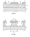
- Fig. 1A and Fig. 1B are cross-sectional views showing a method for producing a wiring of a printed wiring board according to one embodiment of the present invention.
- An etchant used according to the present invention is an acidic type etchant that contains a cupric ion source and hydrochloric acid as main components.
- cupric ion source copper chloride, copper hydroxide, copper sulfate, copper bromide, organic acid cuprate and the like are available.
- copper chloride cupric chloride
- the use of copper chloride (cupric chloride) is preferable because it can increase the stability of an etching rate.
- the concentration of the cupric ion source is 14 to 155 g/liter in terms of the concentration of copper ions, preferably 33 to 122 g/liter. In the case of the concentration becoming too low, the etching rate deteriorates. On the other hand, a too-high concentration reduces the tendency to dissolve, which makes the etching rate unstable. In the case of cupric chloride being used as the cupric ion source, the concentration of the cupric chloride is 30 to 330 g/liter, preferably 70 to 260 g/liter.
- the etchant contains hydrochloric acid.
- a concentration of the hydrochloric acid is 7 to 180 g/liter, preferably 18 to 110 g/liter.
- a too-low concentration of hydrochloric acid results in a failure to obtain a stable etching rate, and a too-high concentration degrades the dissolving stability of copper and might cause the generation of reoxidation on a surface of the copper.
- tetrazole containing nitrogen atoms only as heteroatoms residing in a ring is added.
- the tetrazole may be a monocyclic compound or a compound with condensed rings. Two or more of these tetrazoles may be combined for the use.
- Available tetrazole based compounds include:1H-tetrazole, 5-amino-1H-tetrazole, 5-methyl-1H-tetrazole, 5-phenyl-1H-tetrazole, 5-mercapto-1H-tetrazole, 1-phenyl-5-mercapto-1H-tetrazole, 1-cyclohexyl-5-mercapto-1H-tetrazole and 5, 5'-bis-1H-tetrazole, for example.
- 5-methyl-1H-tetrazole, 5-phenyl-1H-tetrazole and 5-amino-1H-tetrazole are preferable.
- 5-phenyl-1H-tetrazole and 5-amino-1H-tetrazole are preferable.
- the concentration of the tetrazole is 0.1 to 50 g/liter, preferably 0.1 to 15 g/liter, and more preferably 0.2 to 10 g/liter.
- a too-low concentration makes the suppression of undercut insufficient and a too-high concentration degrades an etching rate.
- the etchant used according to the present invention may contain at least one selected from the group consisting of a cationic surface active agent, glycol and glycol ether in order to enhance the stability of the solution and to conduct etching uniformly so that the surface configuration after the etching is uniform.
- a cationic surface active agent alkyl-type quaternary ammonium salts such as benzalkonium chloride and alkyltrimethylammonium chloride, for example, are available.
- the glycol ethylene glycol, diethylene glycol, propylene glycol, polyalkylene glycol and the like are available, for example.
- glycol ether propylene glycol monomethyl ether, ethylene glycol monobutyl ether, 3-methyl-3-methoxybutanol, dipropylene glycol methyl ether, diethylene glycol butyl ether and the like are available, for example.
- the etchant used according to the present invention may contain a solvent other than the above-stated glycol and glycol ether, a surface active agent other than the above-stated cationic surface active agent and various additives as needed.
- the etchant further may include various additives as needed.
- the additives include: a solvent including alcohols such as methanol, ethanol, 1-propanol, 2-propanol, butanol and benzyl alcohol, amides such as N, N-dimethylformamide, dimethyl imidazolidinon and N-methyl pyrrolidone and sulfoxides such as dimethyl sulfoxide; anion surface active agents such as fatty acid salt, alkyl sulfate ester salt and alkylphosphate; nonionic surface active agents such as polyoxyethylene alkyl ether, polyoxypropylene alkyl ether and a block polymer of polyoxyethylene and polyoxypropylene; and ampholytic surface active agents including betains such as lauryl dimethyl aminoacetic acid betain, stearyl dimethyl aminoacetic acid betain, lauryl dimethylamine oxide
- the etchant used according to the method of the present invention can be prepared easily by dissolving the above-stated respective components in water.
- water ion-exchanged water, pure water, ultrapure water and the like whose ionic substances and impurities have been removed are preferable.
- the replenishment solution contains 7 to 360 g/liter (preferably, 30 to 360 g/liter) of hydrochloric acid and 0.1 to 50 g/liter (preferably, 0.2 to 30 g/liter) of azole containing nitrogen atoms only as heteroatoms residing in a ring.
- the replenishment solution added allows the ratio of the respective components in the etchant to be maintained appropriately, whereby a wiring pattern with reduced undercut can be formed stably.
- the replenishment solution further may contain a cupric ion source such as cupric chloride, in which the concentration of the cupric ion source does not exceed 14g/liter in terms of the concentration of copper ions.
- the method otherwise is not limited especially, and available methods include a method of spraying it at a portion of a copper layer on an insulative material that is not covered with an etching resist, and a method of immersing an object to be processed in the etchant. Furthermore, in order to enhance the wettabiltiy of the etchant, prior to the processing with the etchant of the present invention, a surface of copper or copper alloys may be wetted in advance with water, hydrochloric acid with a low concentration or the above-stated replenishment solution.
- a temperature of the etchant during the etching of copper preferably is 30 to 50°C.
- a temperature of the etchant is kept at 30 to 50°C and the spraying is carried out under a spraying pressure of 0.03 to 0.3 MPa.
- a spraying pressure 0.03 to 0.3 MPa.
- the etching of copper or copper alloys is carried out while the above-described replenishment solution is added to the etchant so that the concentration of copper ions in the etchant can be kept at 155 g/liter or lower, preferably, at 122 g/liter or lower. This can prevent the deposition of copper crystals.
- the concentration of copper ions preferably is measured by titration, a conductometric method and the like.
- the etched portion preferably is washed with a cleaning fluid that is capable of dissolving the components of the etchant.
- a cleaning fluid that is capable of dissolving the components of the etchant.
- the cleaning fluid at least one solution selected from the group consisting of an acid solution, a solution containing a substance that is capable of forming a complex compound with copper ions and an organic solution is preferable.
- the residual components including the cupric ion source (cupric chloride and the like) in the etchant and cuprous chloride and copper oxide generated by the reaction especially can be removed with efficiency.
- the cleaning is carried out with an organic solution, the residual components of azole in the etchant especially can be removed with efficiency.
- pH of the solution used preferably is adjusted to 4 or less by using hydrochloric acid, a mixed solution of hydrogen peroxide and sulfuric acid and the like.
- a preferable temperature of the cleaning fluid in that case is 15 to 50°C, and preferable cleaning methods include spray cleaning, ultrasonic cleaning, immersion cleaning and the like.
- an aqueous solution containing 20 to 200 g/liter of ammonia, monoethanolamine and the like preferably is used.
- a preferable temperature of the cleaning fluid in that case is 15 to 50°C, and preferable cleaning methods include spray cleaning, ultrasonic cleaning and the like.
- the organic solution is used as the cleaning fluid
- dipropylene glycol monomethylether and the like preferably are used, and a mixed solution of these organic solutions with water also is preferable.
- a preferable temperature of the cleaning fluid in that case is 15 to 50°C, and preferable cleaning methods include spray cleaning, ultrasonic cleaning and the like.
- the method of the present invention is useful especially for producing a printed wiring board with a copper wiring pattern formed by etching.
- the etchant is useful when an etching resist is formed on a copper foil, an electroless copper plating film, an electrolytic copper plating film, a sputtered copper film or a multilayer film of them, which are formed on an insulative base material, and copper is etched at a portion that is not covered with the etching resist so as to form a wiring pattern.
- a thickness of the etching resist preferably is 40 ⁇ m or less. A too-large thickness degrades an etching rate.
- a rigid board, a flexible board, a metal core board and a ceramic board are available, for example.
- a resist including a so-called dry film and a liquid resist, made of resin, and a resist including a single layer of nickel or a plurality of metal layers, e.g., nickel/gold are available, for example.
- the method of the present invention is useful especially for producing a copper wiring of a substrate on which semiconductor chips are mounted directly, such as a CSP substrate, a TAB substrate and a buildup substrate.
- Fig. 1 shows cross-sectional views of a method for producing a wiring of a printed wiring board according to one embodiment of the present invention, where Fig. 1A shows a cross section of the printed wiring board prior to etching and Fig. 1B shows a cross section of the same subjected to the etching.
- reference numeral 1 denotes an electrical insulative member such as a so-called glass epoxy base material in which glass fiber cloth is impregnated with epoxy resin, a so-called phenol paper base material in which paper is impregnated with phenol resin, a so-called aramid epoxy base material in which aramid fiber non-woven cloth is impregnated with epoxy resin, polyimide film and ceramic base material.
- Reference numeral 2 denotes a copper layer and 3 denotes an etching resist.
- a portion 2a (See Fig. 1A ) of the copper layer 2 on the electrical insulative member 1 that is not covered with the etching resist 3 is etched with the above-described etchant of the present invention so as to form a wiring 4 (See Fig. 1B ).
- a difference between a width W 1 of a top portion of the wiring 4 and a width W 2 of a base portion of the wiring 4 i.e., (W 2 -W 1 ) can be reduced.
- Example 1 Components indicated in Tables 1 and 2 were mixed so as to prepare etchants of Examples 1 to 9 and Comparative Examples 1 to 3.
- the etchant of Example 1 had a specific gravity of 1.13 (at 40°C) and an oxidation-reduction potential of 550 mV.
- etchants indicated in Tables 1 and 2 were sprayed under the conditions of 40°C and a spraying pressure of 0.15 MPa so as to etch the copper foil, whereby copper wiring patterns were formed. Subsequently, 3wt% of aqueous sodium hydroxide was sprayed thereto so as to peel off the dry film resist.
- cupric chloride 300g/liter hydrochloric acid 20g/liter (as HCl) 5-amino-1H-tetrazole 1.5g/liter 2-phenoxyethanol 1g/liter ion-exchanged water remainder 3 8 cupric chloride 150g/liter hydrochloric acid 50g/liter (as HCl) 5-phenyl-1H-tetrazole 0.3g/liter propylene glycol monomethyl ether 15 g/liter ion-exchanged water remainder 3.5
- cupric chloride 150g/liter hydrochloric acid 50g/liter (as HCl) 2-aminobenzothiazole 3g/liter ion-exchanged water remainder 12 Comp.
- the present invention is applicable to various wirings as well, such as a wiring on a glass board, a wiring on a surface of a plastic board and a wiring on a surface of a semiconductor.
Claims (8)
- Procédé de fabrication d'un câblage par attaque du cuivre ou d'alliages de cuivre, comprenant l'étape d'attaque d'une partie d'une couche de cuivre sur un élément électriquement isolant qui est non couvert d'un élément résistant à l'attaque en utilisant un agent d'attaque comprenant une solution aqueuse comprenant :entre 14 et 155 g/litre d'une source d'ions cuivrique en terme de concentration en ions cuivre ;entre 7 et 180 g/litre d'acide chlorhydrique, etentre 0,1 et 50 g/litre d'un composé basé sur du tétrazole etet dans lequel l'agent d'attaque est utilisé de manière répétée et une solution de remplissage est ajoutée à l'agent d'attaque de manière à ce que la concentration en ions cuivre dans l'agent d'attaque peut être maintenue à 155 g/litre ou moins, la solution de remplissage comprenant une solution aqueuse comprenant : entre 7 et 360 g/litres d'acide chlorhydrique ; et entre 0,1 et 50 g/litre d'un composé basé sur du tétrazole.
- Procédé de fabrication d'un câblage selon la revendication 1, dans lequel la solution de remplissage est ajoutée à l'agent d'attaque de manière à ce que la concentration en ions cuivre dans l'agent d'attaque soit maintenue à 122 g/litres ou moins.
- Procédé de fabrication d'un câblage selon la revendication 1, dans lequel après l'attaque du cuivre ou des alliages de cuivre en utilisant l'agent d'attaque, la partie attaquée est lavée avec un fluide de nettoyage qui est capable de dissoudre les composés de l'agent d'attaque.
- Procédé de fabrication d'un câblage selon la revendication 3, dans lequel le fluide de nettoyage est au moins une solution sélectionnée parmi le groupe consistant en une solution acide, une solution contenant une substance qui est capable de former un complexe avec des ions cuivre et une solution organique.
- Procédé de fabrication d'un câblage selon la revendication 1, dans lequel le cuivre et les alliages de cuivre sont attaqués en même que de l'air est soufflée dans l'agent d'attaque.
- Procédé de fabrication d'un câblage selon les revendications 1 à 5, dans lequel entre 0,1 et 15 g/litre de tetrazole est présent.
- Procédé de fabrication d'un câblage selon les revendications 1 à 6, dans lequel la solution d'attaque aqueuse comprend en outre au moins un élément sélectionné parmi le groupe consistant en un agent tensio-actif cationique, un glycol et un éther de glycol.
- Procédé de fabrication d'un câblage selon les revendications 1 à 7, dans lequel entre 30 et 300 g/litre de chlorure cuivrique est présent en tant que source d'ions cuivrique.
Priority Applications (1)
| Application Number | Priority Date | Filing Date | Title |
|---|---|---|---|
| EP10006632A EP2226410A1 (fr) | 2003-07-25 | 2004-07-21 | Solution de décapage, solution de remontage et méthode pour fabriquer des cablages en cuivre |
Applications Claiming Priority (4)
| Application Number | Priority Date | Filing Date | Title |
|---|---|---|---|
| JP2003280118 | 2003-07-25 | ||
| JP2003280118 | 2003-07-25 | ||
| JP2004124375 | 2004-04-20 | ||
| JP2004124375 | 2004-04-20 |
Related Child Applications (1)
| Application Number | Title | Priority Date | Filing Date |
|---|---|---|---|
| EP10006632.3 Division-Into | 2010-06-25 |
Publications (2)
| Publication Number | Publication Date |
|---|---|
| EP1500719A1 EP1500719A1 (fr) | 2005-01-26 |
| EP1500719B1 true EP1500719B1 (fr) | 2011-01-05 |
Family
ID=33492510
Family Applications (2)
| Application Number | Title | Priority Date | Filing Date |
|---|---|---|---|
| EP10006632A Withdrawn EP2226410A1 (fr) | 2003-07-25 | 2004-07-21 | Solution de décapage, solution de remontage et méthode pour fabriquer des cablages en cuivre |
| EP04017218A Active EP1500719B1 (fr) | 2003-07-25 | 2004-07-21 | Méthode pour fabriquer des circuits imprimés en cuivre |
Family Applications Before (1)
| Application Number | Title | Priority Date | Filing Date |
|---|---|---|---|
| EP10006632A Withdrawn EP2226410A1 (fr) | 2003-07-25 | 2004-07-21 | Solution de décapage, solution de remontage et méthode pour fabriquer des cablages en cuivre |
Country Status (8)
| Country | Link |
|---|---|
| US (1) | US7431861B2 (fr) |
| EP (2) | EP2226410A1 (fr) |
| KR (2) | KR20050012682A (fr) |
| CN (1) | CN100459068C (fr) |
| DE (1) | DE602004030861D1 (fr) |
| HK (1) | HK1074224A1 (fr) |
| SG (1) | SG108989A1 (fr) |
| TW (1) | TWI282377B (fr) |
Families Citing this family (40)
| Publication number | Priority date | Publication date | Assignee | Title |
|---|---|---|---|---|
| CN1899003B (zh) * | 2004-03-03 | 2010-12-29 | 揖斐电株式会社 | 蚀刻液、蚀刻方法以及印刷电路板 |
| KR101199533B1 (ko) * | 2005-06-22 | 2012-11-09 | 삼성디스플레이 주식회사 | 식각액, 이를 이용하는 배선 형성 방법 및 박막 트랜지스터기판의 제조 방법 |
| US8263539B2 (en) * | 2005-10-28 | 2012-09-11 | Dynaloy, Llc | Dynamic multi-purpose composition for the removal of photoresists and methods for its use |
| US7632796B2 (en) | 2005-10-28 | 2009-12-15 | Dynaloy, Llc | Dynamic multi-purpose composition for the removal of photoresists and method for its use |
| US7674755B2 (en) * | 2005-12-22 | 2010-03-09 | Air Products And Chemicals, Inc. | Formulation for removal of photoresist, etch residue and BARC |
| KR20070088245A (ko) * | 2006-02-24 | 2007-08-29 | 후지필름 가부시키가이샤 | 금속용 연마액 |
| KR101001875B1 (ko) * | 2006-09-30 | 2010-12-17 | 엘지이노텍 주식회사 | 등방성 에칭을 이용한 미세 패턴 형성방법 및 이를 이용하여 제조된 미세패턴이 형성된 반도체 기판 면상 부재 |
| CN100466182C (zh) * | 2007-01-04 | 2009-03-04 | 北京京东方光电科技有限公司 | 金属导线、电极及薄膜晶体管阵列基板的制造方法 |
| US7655608B2 (en) * | 2007-08-03 | 2010-02-02 | Dynaloy, Llc | Reduced metal etch rates using stripper solutions containing a copper salt |
| JP4472006B2 (ja) * | 2007-09-04 | 2010-06-02 | メック株式会社 | エッチング液及び導体パターンの形成方法 |
| JP4916455B2 (ja) * | 2008-01-15 | 2012-04-11 | 株式会社Adeka | 銅含有材料用エッチング剤組成物 |
| WO2009091012A1 (fr) | 2008-01-15 | 2009-07-23 | Mitsubishi Paper Mills Limited | Agent de gravure pour cuivre ou alliage de cuivre, liquide pour prétraitement de gravure, et procédé de gravure |
| WO2009101948A1 (fr) | 2008-02-12 | 2009-08-20 | Mitsubishi Paper Mills Limited | Procédé de gravure |
| KR101135798B1 (ko) * | 2008-02-20 | 2012-04-16 | 멕크 가부시키가이샤 | 에칭액 및 이것을 이용한 구리 배선의 형성 방법 |
| JP4521460B2 (ja) * | 2008-02-20 | 2010-08-11 | メック株式会社 | エッチング液及びこれを用いた銅配線の形成方法 |
| TWI450052B (zh) * | 2008-06-24 | 2014-08-21 | Dynaloy Llc | 用於後段製程操作有效之剝離溶液 |
| JP5443863B2 (ja) * | 2009-07-09 | 2014-03-19 | 株式会社Adeka | 銅含有材料用エッチング剤組成物及び銅含有材料のエッチング方法 |
| JP4685180B2 (ja) * | 2009-07-09 | 2011-05-18 | 株式会社Adeka | 銅含有材料用エッチング剤組成物及び銅含有材料のエッチング方法 |
| CN102762770B (zh) * | 2010-02-15 | 2014-07-16 | 三菱瓦斯化学株式会社 | 包含铜层及钼层的多层薄膜用蚀刻液 |
| TWI539493B (zh) | 2010-03-08 | 2016-06-21 | 黛納羅伊有限責任公司 | 用於摻雜具有分子單層之矽基材之方法及組合物 |
| JP5667927B2 (ja) * | 2011-05-20 | 2015-02-12 | 富士フイルム株式会社 | マイグレーション抑制層形成用処理液、および、マイグレーション抑制層を有する積層体の製造方法 |
| CN102291952B (zh) * | 2011-08-05 | 2013-04-24 | 奥士康精密电路(惠州)有限公司 | 多层pcb板的制备方法 |
| JP2013104104A (ja) * | 2011-11-14 | 2013-05-30 | Mec Kk | エッチング液、補給液及び銅配線の形成方法 |
| CN103255417B (zh) * | 2011-12-16 | 2016-01-20 | 江阴润玛电子材料股份有限公司 | 一种酸性钼铝钼蚀刻液及其制备工艺 |
| US8877075B2 (en) | 2012-02-01 | 2014-11-04 | Infineon Technologies Ag | Apparatuses and methods for gas mixed liquid polishing, etching, and cleaning |
| CN104769159B (zh) * | 2012-12-03 | 2017-09-19 | Mec股份有限公司 | 蚀刻液、补给液及铜配线的形成方法 |
| JP5576525B1 (ja) * | 2013-03-29 | 2014-08-20 | メルテックス株式会社 | 銅エッチング液 |
| US9301399B2 (en) * | 2013-04-23 | 2016-03-29 | Mitsubishi Gas Chemical Company, Inc. | Method of treating wiring substrate and wiring substrate manufactured by the same |
| KR101318733B1 (ko) * | 2013-06-13 | 2013-10-18 | 주식회사 에이씨엠 | 구리 유기 착물을 이용한 에칭제 조성물 |
| TWI487811B (zh) * | 2013-11-27 | 2015-06-11 | Chem Entpr Corp E | 可有效減緩賈凡尼效應之蝕刻液 |
| CN103952702A (zh) * | 2014-05-04 | 2014-07-30 | 深圳市实锐泰科技有限公司 | 蚀刻液及使用该蚀刻液进行软性线路板细线蚀刻的方法 |
| CN104278273A (zh) * | 2014-06-13 | 2015-01-14 | 叶涛 | 线路板低酸高效型酸性氯化铜蚀刻液 |
| JP6000420B1 (ja) | 2015-08-31 | 2016-09-28 | メック株式会社 | エッチング液、補給液及び銅配線の形成方法 |
| CN105479965B (zh) * | 2015-12-16 | 2018-12-25 | 东莞运城制版有限公司 | 一种版辊的氯化铜腐蚀装置及腐蚀方法 |
| US20210381111A1 (en) * | 2018-02-01 | 2021-12-09 | Mitsubishi Gas Chemical Company, Inc. | Aqueous solution for surface treatment, method for producing surface-treated alloy, and composite and method for producing the same |
| CN111155091A (zh) * | 2020-02-13 | 2020-05-15 | Tcl华星光电技术有限公司 | 蚀刻液、添加剂及金属布线的制作方法 |
| CN114381736A (zh) * | 2022-01-07 | 2022-04-22 | 安捷利(番禺)电子实业有限公司 | 一种钛铜合金蚀刻液及蚀刻方法 |
| CN114672807A (zh) * | 2022-05-26 | 2022-06-28 | 深圳市板明科技股份有限公司 | 一种高铜含量的有机酸超粗化微蚀液及其应用 |
| CN115323377B (zh) * | 2022-08-31 | 2023-11-24 | 昆山市板明电子科技有限公司 | 一种闪蚀药水及其制备方法 |
| CN116732520B (zh) * | 2023-08-14 | 2023-11-14 | 昆山市板明电子科技有限公司 | 酸性蚀刻液用长效抑制侧蚀添加剂、制备方法及应用 |
Family Cites Families (18)
| Publication number | Priority date | Publication date | Assignee | Title |
|---|---|---|---|---|
| JPS5221460B1 (fr) * | 1971-04-26 | 1977-06-10 | ||
| DE2557269A1 (de) | 1975-12-19 | 1977-06-30 | Licentia Gmbh | Verfahren zum aetzen von kupfer oder kupferlegierungen |
| DE3623504A1 (de) * | 1986-07-09 | 1988-01-21 | Schering Ag | Kupferaetzloesungen |
| JPS63121679A (ja) * | 1986-11-10 | 1988-05-25 | Sumitomo Precision Prod Co Ltd | 塩化第二銅エツチング液の再生方法 |
| JP3387528B2 (ja) | 1992-08-07 | 2003-03-17 | 朝日化学工業株式会社 | 銅または銅合金のエッチング用組成物およびそのエッチング方法 |
| JP3225471B2 (ja) * | 1992-12-24 | 2001-11-05 | 旭電化工業株式会社 | 銅溶解剤 |
| JPH06312679A (ja) * | 1993-04-28 | 1994-11-08 | Suzuki Motor Corp | 自動二輪車の補助灯一体型スピードメータ |
| RU2102530C1 (ru) * | 1994-02-25 | 1998-01-20 | Элеонора Герцевна Зак | Способ очистки и ингибирования изделий из меди и медно-стальной проволоки |
| JP2781954B2 (ja) | 1994-03-04 | 1998-07-30 | メック株式会社 | 銅および銅合金の表面処理剤 |
| JP3109430B2 (ja) | 1996-01-26 | 2000-11-13 | 住友金属工業株式会社 | エッチング処理液の再生方法およびその再生液の使用方法 |
| JP3535755B2 (ja) | 1997-12-25 | 2004-06-07 | キヤノン株式会社 | エッチング方法 |
| US6162366A (en) * | 1997-12-25 | 2000-12-19 | Canon Kabushiki Kaisha | Etching process |
| US6156221A (en) * | 1998-10-02 | 2000-12-05 | International Business Machines Corporation | Copper etching compositions, processes and products derived therefrom |
| US6444140B2 (en) | 1999-03-17 | 2002-09-03 | Morton International Inc. | Micro-etch solution for producing metal surface topography |
| JP2000282265A (ja) * | 1999-03-31 | 2000-10-10 | Mec Kk | 銅または銅合金のマイクロエッチング剤およびそれを用いる表面処理法 |
| US6410442B1 (en) * | 1999-08-18 | 2002-06-25 | Advanced Micro Devices, Inc. | Mask-less differential etching and planarization of copper films |
| JP4687852B2 (ja) * | 2001-06-25 | 2011-05-25 | 三菱瓦斯化学株式会社 | 銅および銅合金の表面処理剤 |
| JP2003105569A (ja) | 2001-09-28 | 2003-04-09 | Asahi Denka Kogyo Kk | 銅含有金属材料表面粗化剤及び銅含有金属材料の表面処理方法 |
-
2004
- 2004-07-19 TW TW093121488A patent/TWI282377B/zh active
- 2004-07-21 EP EP10006632A patent/EP2226410A1/fr not_active Withdrawn
- 2004-07-21 DE DE602004030861T patent/DE602004030861D1/de active Active
- 2004-07-21 EP EP04017218A patent/EP1500719B1/fr active Active
- 2004-07-22 US US10/896,465 patent/US7431861B2/en active Active
- 2004-07-23 SG SG200404344A patent/SG108989A1/en unknown
- 2004-07-23 KR KR1020040057740A patent/KR20050012682A/ko not_active Application Discontinuation
- 2004-07-26 CN CNB2004100586404A patent/CN100459068C/zh active Active
-
2005
- 2005-08-02 HK HK05106603.1A patent/HK1074224A1/xx unknown
-
2008
- 2008-04-28 KR KR1020080039452A patent/KR100946873B1/ko active IP Right Grant
Also Published As
| Publication number | Publication date |
|---|---|
| TW200504245A (en) | 2005-02-01 |
| EP2226410A1 (fr) | 2010-09-08 |
| KR20080056117A (ko) | 2008-06-20 |
| CN100459068C (zh) | 2009-02-04 |
| US7431861B2 (en) | 2008-10-07 |
| US20050016961A1 (en) | 2005-01-27 |
| EP1500719A1 (fr) | 2005-01-26 |
| TWI282377B (en) | 2007-06-11 |
| CN1576395A (zh) | 2005-02-09 |
| HK1074224A1 (en) | 2005-11-04 |
| SG108989A1 (en) | 2005-02-28 |
| DE602004030861D1 (de) | 2011-02-17 |
| KR100946873B1 (ko) | 2010-03-09 |
| KR20050012682A (ko) | 2005-02-02 |
Similar Documents
| Publication | Publication Date | Title |
|---|---|---|
| EP1500719B1 (fr) | Méthode pour fabriquer des circuits imprimés en cuivre | |
| JP4224436B2 (ja) | エッチング剤と補給液及びこれを用いた銅配線の製造方法 | |
| JP4472006B2 (ja) | エッチング液及び導体パターンの形成方法 | |
| EP0670379B1 (fr) | Procédé de micro-gravure de surfaces en cuivre ou alliages de cuivre | |
| JP4629048B2 (ja) | 銅および混合金属回路の微細粗面化処理のための改良された方法 | |
| JP5505847B2 (ja) | エッチング剤 | |
| KR100868137B1 (ko) | 구리 및 구리 합금의 표면 처리제 | |
| JP3387528B2 (ja) | 銅または銅合金のエッチング用組成物およびそのエッチング方法 | |
| EP3680363B1 (fr) | Agent de microgravure pour cuivre, procédé de rugosification de surface de cuivre et procédé de production de carte de câblage | |
| JP2006111953A (ja) | 銅又は銅合金のエッチング剤、その製造法、補給液及び配線基板の製造法 | |
| EP2878706B1 (fr) | Agent de microgravure pour le cuivre, liquide de supplément pour celui-ci, et procédé de fabrication pour carte de circuit imprimé | |
| KR101162370B1 (ko) | 세미 어디티브법 프린트 배선 기판의 제조에서의 에칭 제거방법 및 에칭액 | |
| TW201320843A (zh) | 蝕刻液、補給液及銅配線之形成方法 | |
| KR20150109932A (ko) | 에칭액 조성물 및 이를 이용한 회로 패턴의 제조방법 | |
| KR20150059602A (ko) | 에칭용 조성물 및 이것을 이용한 프린트 배선판의 제조방법 | |
| JP2007180172A (ja) | 基板の製造方法 | |
| JP2011233769A (ja) | 銅配線パターンの形成方法 | |
| JP2003338676A (ja) | 銅配線基板の製造方法 | |
| JP5005883B2 (ja) | サブトラクティブ工法用回路形成エッチング液 | |
| JP4069387B2 (ja) | エッチング液 | |
| JP4431860B2 (ja) | 銅および銅合金の表面処理剤 | |
| KR102124328B1 (ko) | 구리 금속 표면의 밀착 향상용 미세 조도 형성 조성물 | |
| WO2023163003A1 (fr) | Composition de gravure et procédé de production de carte de câblage l'utilisant | |
| JP2011084781A (ja) | 導体パターンの形成方法 | |
| KR19980066842A (ko) | 구리 또는 구리합금에 대한 마이크로에칭 조성물 |
Legal Events
| Date | Code | Title | Description |
|---|---|---|---|
| PUAI | Public reference made under article 153(3) epc to a published international application that has entered the european phase |
Free format text: ORIGINAL CODE: 0009012 |
|
| AK | Designated contracting states |
Kind code of ref document: A1 Designated state(s): AT BE BG CH CY CZ DE DK EE ES FI FR GB GR HU IE IT LI LU MC NL PL PT RO SE SI SK TR |
|
| AX | Request for extension of the european patent |
Extension state: AL HR LT LV MK |
|
| 17P | Request for examination filed |
Effective date: 20050425 |
|
| AKX | Designation fees paid |
Designated state(s): BE DE FR |
|
| 17Q | First examination report despatched |
Effective date: 20060316 |
|
| GRAP | Despatch of communication of intention to grant a patent |
Free format text: ORIGINAL CODE: EPIDOSNIGR1 |
|
| RTI1 | Title (correction) |
Free format text: METHOD FOR PRODUCING COPPER WIRING |
|
| GRAS | Grant fee paid |
Free format text: ORIGINAL CODE: EPIDOSNIGR3 |
|
| GRAA | (expected) grant |
Free format text: ORIGINAL CODE: 0009210 |
|
| AK | Designated contracting states |
Kind code of ref document: B1 Designated state(s): BE DE FR |
|
| REF | Corresponds to: |
Ref document number: 602004030861 Country of ref document: DE Date of ref document: 20110217 Kind code of ref document: P |
|
| REG | Reference to a national code |
Ref country code: DE Ref legal event code: R096 Ref document number: 602004030861 Country of ref document: DE Effective date: 20110217 |
|
| PLBE | No opposition filed within time limit |
Free format text: ORIGINAL CODE: 0009261 |
|
| STAA | Information on the status of an ep patent application or granted ep patent |
Free format text: STATUS: NO OPPOSITION FILED WITHIN TIME LIMIT |
|
| 26N | No opposition filed |
Effective date: 20111006 |
|
| REG | Reference to a national code |
Ref country code: DE Ref legal event code: R097 Ref document number: 602004030861 Country of ref document: DE Effective date: 20111006 |
|
| REG | Reference to a national code |
Ref country code: FR Ref legal event code: ST Effective date: 20120330 |
|
| PG25 | Lapsed in a contracting state [announced via postgrant information from national office to epo] |
Ref country code: FR Free format text: LAPSE BECAUSE OF NON-PAYMENT OF DUE FEES Effective date: 20110801 |
|
| P01 | Opt-out of the competence of the unified patent court (upc) registered |
Effective date: 20230410 |
|
| PGFP | Annual fee paid to national office [announced via postgrant information from national office to epo] |
Ref country code: DE Payment date: 20230719 Year of fee payment: 20 Ref country code: BE Payment date: 20230719 Year of fee payment: 20 |