JP4629048B2 - 銅および混合金属回路の微細粗面化処理のための改良された方法 - Google Patents
銅および混合金属回路の微細粗面化処理のための改良された方法 Download PDFInfo
- Publication number
- JP4629048B2 JP4629048B2 JP2006534003A JP2006534003A JP4629048B2 JP 4629048 B2 JP4629048 B2 JP 4629048B2 JP 2006534003 A JP2006534003 A JP 2006534003A JP 2006534003 A JP2006534003 A JP 2006534003A JP 4629048 B2 JP4629048 B2 JP 4629048B2
- Authority
- JP
- Japan
- Prior art keywords
- metal
- roughening
- copper
- micro
- metal layer
- Prior art date
- Legal status (The legal status is an assumption and is not a legal conclusion. Google has not performed a legal analysis and makes no representation as to the accuracy of the status listed.)
- Expired - Fee Related
Links
Images


Classifications
-
- H—ELECTRICITY
- H05—ELECTRIC TECHNIQUES NOT OTHERWISE PROVIDED FOR
- H05K—PRINTED CIRCUITS; CASINGS OR CONSTRUCTIONAL DETAILS OF ELECTRIC APPARATUS; MANUFACTURE OF ASSEMBLAGES OF ELECTRICAL COMPONENTS
- H05K3/00—Apparatus or processes for manufacturing printed circuits
- H05K3/02—Apparatus or processes for manufacturing printed circuits in which the conductive material is applied to the surface of the insulating support and is thereafter removed from such areas of the surface which are not intended for current conducting or shielding
- H05K3/06—Apparatus or processes for manufacturing printed circuits in which the conductive material is applied to the surface of the insulating support and is thereafter removed from such areas of the surface which are not intended for current conducting or shielding the conductive material being removed chemically or electrolytically, e.g. by photo-etch process
-
- C—CHEMISTRY; METALLURGY
- C23—COATING METALLIC MATERIAL; COATING MATERIAL WITH METALLIC MATERIAL; CHEMICAL SURFACE TREATMENT; DIFFUSION TREATMENT OF METALLIC MATERIAL; COATING BY VACUUM EVAPORATION, BY SPUTTERING, BY ION IMPLANTATION OR BY CHEMICAL VAPOUR DEPOSITION, IN GENERAL; INHIBITING CORROSION OF METALLIC MATERIAL OR INCRUSTATION IN GENERAL
- C23F—NON-MECHANICAL REMOVAL OF METALLIC MATERIAL FROM SURFACE; INHIBITING CORROSION OF METALLIC MATERIAL OR INCRUSTATION IN GENERAL; MULTI-STEP PROCESSES FOR SURFACE TREATMENT OF METALLIC MATERIAL INVOLVING AT LEAST ONE PROCESS PROVIDED FOR IN CLASS C23 AND AT LEAST ONE PROCESS COVERED BY SUBCLASS C21D OR C22F OR CLASS C25
- C23F1/00—Etching metallic material by chemical means
- C23F1/10—Etching compositions
- C23F1/14—Aqueous compositions
- C23F1/16—Acidic compositions
- C23F1/18—Acidic compositions for etching copper or alloys thereof
-
- H—ELECTRICITY
- H05—ELECTRIC TECHNIQUES NOT OTHERWISE PROVIDED FOR
- H05K—PRINTED CIRCUITS; CASINGS OR CONSTRUCTIONAL DETAILS OF ELECTRIC APPARATUS; MANUFACTURE OF ASSEMBLAGES OF ELECTRICAL COMPONENTS
- H05K3/00—Apparatus or processes for manufacturing printed circuits
- H05K3/38—Improvement of the adhesion between the insulating substrate and the metal
- H05K3/382—Improvement of the adhesion between the insulating substrate and the metal by special treatment of the metal
- H05K3/383—Improvement of the adhesion between the insulating substrate and the metal by special treatment of the metal by microetching
-
- H—ELECTRICITY
- H05—ELECTRIC TECHNIQUES NOT OTHERWISE PROVIDED FOR
- H05K—PRINTED CIRCUITS; CASINGS OR CONSTRUCTIONAL DETAILS OF ELECTRIC APPARATUS; MANUFACTURE OF ASSEMBLAGES OF ELECTRICAL COMPONENTS
- H05K2201/00—Indexing scheme relating to printed circuits covered by H05K1/00
- H05K2201/03—Conductive materials
- H05K2201/0332—Structure of the conductor
- H05K2201/0335—Layered conductors or foils
- H05K2201/0338—Layered conductor, e.g. layered metal substrate, layered finish layer, layered thin film adhesion layer
-
- H—ELECTRICITY
- H05—ELECTRIC TECHNIQUES NOT OTHERWISE PROVIDED FOR
- H05K—PRINTED CIRCUITS; CASINGS OR CONSTRUCTIONAL DETAILS OF ELECTRIC APPARATUS; MANUFACTURE OF ASSEMBLAGES OF ELECTRICAL COMPONENTS
- H05K2201/00—Indexing scheme relating to printed circuits covered by H05K1/00
- H05K2201/06—Thermal details
- H05K2201/068—Thermal details wherein the coefficient of thermal expansion is important
-
- H—ELECTRICITY
- H05—ELECTRIC TECHNIQUES NOT OTHERWISE PROVIDED FOR
- H05K—PRINTED CIRCUITS; CASINGS OR CONSTRUCTIONAL DETAILS OF ELECTRIC APPARATUS; MANUFACTURE OF ASSEMBLAGES OF ELECTRICAL COMPONENTS
- H05K2203/00—Indexing scheme relating to apparatus or processes for manufacturing printed circuits covered by H05K3/00
- H05K2203/12—Using specific substances
- H05K2203/122—Organic non-polymeric compounds, e.g. oil, wax, thiol
- H05K2203/124—Heterocyclic organic compounds, e.g. azole, furan
-
- H—ELECTRICITY
- H05—ELECTRIC TECHNIQUES NOT OTHERWISE PROVIDED FOR
- H05K—PRINTED CIRCUITS; CASINGS OR CONSTRUCTIONAL DETAILS OF ELECTRIC APPARATUS; MANUFACTURE OF ASSEMBLAGES OF ELECTRICAL COMPONENTS
- H05K3/00—Apparatus or processes for manufacturing printed circuits
- H05K3/02—Apparatus or processes for manufacturing printed circuits in which the conductive material is applied to the surface of the insulating support and is thereafter removed from such areas of the surface which are not intended for current conducting or shielding
- H05K3/022—Processes for manufacturing precursors of printed circuits, i.e. copper-clad substrates
-
- H—ELECTRICITY
- H05—ELECTRIC TECHNIQUES NOT OTHERWISE PROVIDED FOR
- H05K—PRINTED CIRCUITS; CASINGS OR CONSTRUCTIONAL DETAILS OF ELECTRIC APPARATUS; MANUFACTURE OF ASSEMBLAGES OF ELECTRICAL COMPONENTS
- H05K3/00—Apparatus or processes for manufacturing printed circuits
- H05K3/02—Apparatus or processes for manufacturing printed circuits in which the conductive material is applied to the surface of the insulating support and is thereafter removed from such areas of the surface which are not intended for current conducting or shielding
- H05K3/06—Apparatus or processes for manufacturing printed circuits in which the conductive material is applied to the surface of the insulating support and is thereafter removed from such areas of the surface which are not intended for current conducting or shielding the conductive material being removed chemically or electrolytically, e.g. by photo-etch process
- H05K3/061—Etching masks
- H05K3/064—Photoresists
-
- H—ELECTRICITY
- H05—ELECTRIC TECHNIQUES NOT OTHERWISE PROVIDED FOR
- H05K—PRINTED CIRCUITS; CASINGS OR CONSTRUCTIONAL DETAILS OF ELECTRIC APPARATUS; MANUFACTURE OF ASSEMBLAGES OF ELECTRICAL COMPONENTS
- H05K3/00—Apparatus or processes for manufacturing printed circuits
- H05K3/46—Manufacturing multilayer circuits
- H05K3/4611—Manufacturing multilayer circuits by laminating two or more circuit boards
- H05K3/4641—Manufacturing multilayer circuits by laminating two or more circuit boards having integrally laminated metal sheets or special power cores
Description
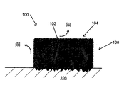
図2は、混合金属回路パターン素子202を含む初期のプリント回路200を微細粗面化する場合の、上記影響を説明する概略断面図である。回路パターン素子202は、上面204および側面206を含み、銅のような金属の外層210、鉄またはインバー等の他の金属の第2層すなわち内層212、および外層210の金属と同一または異なり得る金属の基層214を含む。図2に示す例においては、外層210および基層214は、共に銅または銅合金で構成される。3つの金属層は複合体、あるいは混合金属層216を形成する。素子202は、混合金属層における回路パターンを例えばエッチングする形成プロセスにより形成されており、より大きな回路パターンの素子を形成する。この例における回路素子202は、誘電体基材208に付着している。
この連続した工程において、金属層全体の厚みを減少させる2つのエッチング工程(工程2および9)と、金属のパターン幅に影響を与える2つのエッチング工程(工程5および9)がある。
a.第1主面を有しパターン形成されていない金属層を提供すること;
b.パターン形成されていない金属層に微細粗面化溶液を用いて微細粗面化を施し、第1主面に微細粗面化された表面を形成すること;
c.微細粗面化された表面にエッチレジストを適用すること;
d.エッチレジストをパターニングし、除去する金属範囲を露出させること;
e.エッチレジストにより保護されていない金属層をエッチングし、回路パターンを形成すること;および、
f.エッチレジストを除去することを含む、誘電体材料の金属層への密着性を改善するプロセスに関する。
a.第1主面を有しパターン形成されていない金属層を提供すること;
b.パターン形成されていない金属層に微細粗面化溶液を用い微細粗面化を施し、第1主面に微細粗面化された表面を形成すること;
c.微細粗面化された表面にエッチレジストを適用すること;
d.エッチレジストをパターニングし、除去すべき金属範囲を露出させること;
e.エッチレジストにより保護されていない金属層をエッチングし、回路パターンを形成すること;
f.エッチレジストを除去すること;
g.微細粗面化された表面に第2の金属コーティングを必要に応じて適用すること;および、
h.微細粗面化された表面に誘電体を適用することを含む、誘電体材料の金属層への密着性を改善するプロセスに関する。
a.第1主面を有しパターン形成されていない金属層を提供すること;
b.パターン形成されていない金属層に溶液を用いて微細粗面化を施し、第1主面に微細粗面化された表面を形成すること;
c.微細粗面化された表面にエッチレジストを適応すること;
d.エッチレジストをパターニングし、除去すべき金属範囲を露出させること;
e.エッチレジストにより保護されていない金属層をエッチングし、回路パターンを形成すること;および、
f.エッチレジストを除去することを含む、誘電体材料の金属層への密着性を改善するプロセスに関する。
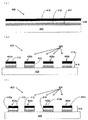
本発明の第2の実施形態におけるプロセスを、図7a〜7cを参照して説明する。図7a〜7cは、本発明の実施形態によるプロセスの概略断面図であり、混合金属層の表面を微細粗面化することに続いて、層をエッチングして回路パターン素子を形成することを含む。
Instruments, Inc.およびGould
Electronics, Inc.から市販品されており、様々なインレー比(inlay ratio)の被覆原材料として提供される。CICについてのインレー比は、例えば約12.5%/75%/12.5%から約30%/40%/30%の範囲であり得、例えば、20%/60%/20%を含む。CICおよび類似の混合金属層は、例えば約6mil(約0.15mm)の厚みで提供され得る。CICおよび類似の混合金属層は、必要に応じてロールを通され、適切な厚みへと薄くされ得る。
別の実施形態においては、回路基板は、銅または銅合金等の単一金属層を含み得る。
数多くの適切な微細粗面化プロセスが、本発明と共に用いることが知られている。いくつかのこのようなプロセスは、以下の開示にて簡潔に示される。これらは例示のみを意図したものであり、本発明はこれらのいずれにも限定される必要はない。

硫酸、濃硫酸(concentrated):10〜250g/l
過酸化水素、30wt%溶液:1〜100g/l
窒素含有複素五員環化合物:0.5〜50g/l
スルフィン酸、セレン酸またはテルル酸を含む粘着成分:0.05〜10g/l
粘着性複素環式化合物:0.05〜20g/l
スルホニウム、セレノニウム(Selenonium)またはテルリウム塩:0.01〜10g/l
Claims (18)
- (a)第1主面を有しパターン形成されていない、銅層と第2の金属層または合金層とを含む金属層を提供すること;
(b)該第1主面に微細粗面化を施し、微細粗面化された表面を形成すること;および、
(e)該金属層をエッチングし、該金属層に回路パターンを形成することを含み、
該微細粗面化がエッチングの前に行われ、該微細粗面化された表面が、粗面計の測定で0.3〜0.6ミクロンの表面粗さraを有し、
該微細粗面化が、(a)過酸化水素;(b)少なくとも1つの酸;(c)硫黄、セレニウムまたはテルリウム原子を複素環に含まない、少なくとも1つの窒素含有複素五員環化合物;ならびに(d)スルフィン酸、セレニン酸、テルリン酸、少なくとも1つの硫黄、セレニウムおよび/またはテルリウム原子を複素環中に含む複素環化合物;および、下記一般式(1)で表されるセレノニウムおよびテルロニウム塩、からなる群から選択される少なくとも1つの粘着剤;を含む水性組成物を適用することにより行われる、誘電体材料の金属層への密着性を改善するプロセス:
- 前記(e)の前に、
(c)微細粗面化された表面にエッチレジストを適用すること;および、
(d)該エッチレジストをパターニングし、除去すべき金属範囲を露出させることをさらに含み、
(e)は該除去すべき金属範囲をエッチングする、請求項1に記載のプロセス。 - 工程(e)に続いて、
(f)前記エッチレジストを除去すること;
(g)前記微細粗面化された表面に第2の金属コーティングを必要に応じて適用すること;および、
(h)該微細粗面化された表面に誘電体を適用することをさらに含む、請求項2に記載のプロセス。 - 前記パターン形成されていない金属層が、前記微細粗面化前に表面粗さを増やす処理を行われない、請求項1から3のいずれかに記載のプロセス。
- 前記微細粗面化された表面が、前記エッチングに続くさらなる粗面化に供されない、請求項1から4のいずれかに記載のプロセス。
- 前記エッチングにより形成された前記回路パターンが断面積を有し、該断面積が該エッチングの後に実質的にさらに減少しない、請求項1から5のいずれかに記載のプロセス。
- 前記微細粗面化の前に前記第1主面を洗浄することをさらに含む、請求項1から6のいずれかに記載のプロセス。
- 前記洗浄後および前記微細粗面化前に、水溶性のアルコールを含む溶液を適用して前記第1主面を前調整することをさらに含む、請求項7に記載のプロセス。
- 前記溶液が、腐食防止剤をさらに含む、請求項8に記載のプロセス。
- 前記エッチングの後に前記エッチレジストを除去することをさらに含む、請求項2に記載のプロセス。
- 前記回路パターンに第2の金属コーティングを適用することをさらに含む、請求項1または2に記載のプロセス。
- 前記回路パターンに誘電体材料を適用することをさらに含む、請求項1または2に記載のプロセス。
- 前記第2の金属が、鉄およびニッケルの合金である、請求項1に記載のプロセス。
- 前記合金が、64原子パーセントの鉄および36原子パーセントのニッケルを含む、請求項13に記載のプロセス。
- 0.5から2ミクロンの金属が、前記微細粗面化工程において除去される、請求項1から14のいずれかに記載のプロセス。
- 前記微細粗面化された表面が、前記第1主面の90%以上をカバーする、請求項1から15のいずれかに記載のプロセス。
- 前記微細粗面化された表面が、前記第1主面の実質的にすべてをカバーする、請求項1から16のいずれかに記載のプロセス。
- 前記金属層が、銅−インバー−銅(CIC)層である、請求項1から17に記載のプロセス。
Applications Claiming Priority (2)
| Application Number | Priority Date | Filing Date | Title |
|---|---|---|---|
| US10/675,019 US20050067378A1 (en) | 2003-09-30 | 2003-09-30 | Method for micro-roughening treatment of copper and mixed-metal circuitry |
| PCT/US2004/031697 WO2005034596A2 (en) | 2003-09-30 | 2004-09-27 | Improved method for micro-roughening treatment of copper and mixed-metal circuitry |
Publications (2)
| Publication Number | Publication Date |
|---|---|
| JP2007507616A JP2007507616A (ja) | 2007-03-29 |
| JP4629048B2 true JP4629048B2 (ja) | 2011-02-09 |
Family
ID=34377021
Family Applications (1)
| Application Number | Title | Priority Date | Filing Date |
|---|---|---|---|
| JP2006534003A Expired - Fee Related JP4629048B2 (ja) | 2003-09-30 | 2004-09-27 | 銅および混合金属回路の微細粗面化処理のための改良された方法 |
Country Status (12)
| Country | Link |
|---|---|
| US (1) | US20050067378A1 (ja) |
| EP (1) | EP1668967B1 (ja) |
| JP (1) | JP4629048B2 (ja) |
| KR (1) | KR101177145B1 (ja) |
| CN (1) | CN100594763C (ja) |
| AT (1) | ATE447837T1 (ja) |
| BR (1) | BRPI0414904A (ja) |
| CA (1) | CA2536836A1 (ja) |
| DE (1) | DE602004023958D1 (ja) |
| MY (1) | MY147004A (ja) |
| TW (1) | TWI347232B (ja) |
| WO (1) | WO2005034596A2 (ja) |
Families Citing this family (44)
| Publication number | Priority date | Publication date | Assignee | Title |
|---|---|---|---|---|
| US7063800B2 (en) * | 2003-11-10 | 2006-06-20 | Ying Ding | Methods of cleaning copper surfaces in the manufacture of printed circuit boards |
| DE102004050269A1 (de) * | 2004-10-14 | 2006-04-20 | Institut Für Solarenergieforschung Gmbh | Verfahren zur Kontakttrennung elektrisch leitfähiger Schichten auf rückkontaktierten Solarzellen und Solarzelle |
| US7307022B2 (en) * | 2004-11-19 | 2007-12-11 | Endicott Interconnect Technologies, Inc. | Method of treating conductive layer for use in a circuitized substrate and method of making said substrate having said conductive layer as part thereof |
| US7383629B2 (en) * | 2004-11-19 | 2008-06-10 | Endicott Interconnect Technologies, Inc. | Method of making circuitized substrates utilizing smooth-sided conductive layers as part thereof |
| DE602006013110D1 (de) * | 2005-03-25 | 2010-05-06 | Dupont Air Prod Nanomaterials | In chemisch-mechanischen reinigungszusammensetzungen verwendete dihydroxy-enol-verbindungen mit metall-ionen-oxidationsmitteln |
| US7591955B2 (en) * | 2005-07-14 | 2009-09-22 | Interplex Nas, Inc. | Method for forming an etched soft edge metal foil and the product thereof |
| EP1820884B1 (en) * | 2006-02-17 | 2009-10-07 | Atotech Deutschland Gmbh | Solution and process to treat surfaces of copper alloys in order to improve the adhesion between the metal surface and the bonded polymeric material |
| US7704562B2 (en) * | 2006-08-14 | 2010-04-27 | Cordani Jr John L | Process for improving the adhesion of polymeric materials to metal surfaces |
| ES2405979T3 (es) * | 2007-04-06 | 2013-06-04 | Taisei Plas Co., Ltd. | Material compuesto de aleación de cobre y procedimiento para fabricarlo |
| JP2009016818A (ja) * | 2007-07-04 | 2009-01-22 | Samsung Electro-Mechanics Co Ltd | 多層印刷回路基板及びその製造方法 |
| US8240036B2 (en) | 2008-04-30 | 2012-08-14 | Panasonic Corporation | Method of producing a circuit board |
| TWI362239B (en) * | 2008-04-30 | 2012-04-11 | Panasonic Elec Works Co Ltd | Method of producing circuit board by additive method, and circuit board and multilayer circuit board obtained by the method |
| JP5203108B2 (ja) | 2008-09-12 | 2013-06-05 | 新光電気工業株式会社 | 配線基板及びその製造方法 |
| DE102008056086A1 (de) * | 2008-11-06 | 2010-05-12 | Gp Solar Gmbh | Additiv für alkalische Ätzlösungen, insbesondere für Texturätzlösungen sowie Verfahren zu dessen Herstellung |
| WO2010067844A1 (ja) | 2008-12-11 | 2010-06-17 | 日立化成工業株式会社 | Cmp用研磨液及びこれを用いた研磨方法 |
| US9332642B2 (en) | 2009-10-30 | 2016-05-03 | Panasonic Corporation | Circuit board |
| CN102598883A (zh) | 2009-10-30 | 2012-07-18 | 松下电器产业株式会社 | 电路板以及在电路板上安装有元件的半导体装置 |
| JP5603600B2 (ja) * | 2010-01-13 | 2014-10-08 | 新光電気工業株式会社 | 配線基板及びその製造方法、並びに半導体パッケージ |
| JP5482285B2 (ja) * | 2010-02-23 | 2014-05-07 | 大日本印刷株式会社 | 配線回路基板用基材、配線回路基板用基材の製造方法、配線回路基板、配線回路基板の製造方法、hdd用サスペンション基板、hdd用サスペンションおよびハードディスクドライブ |
| JP5648567B2 (ja) * | 2010-05-07 | 2015-01-07 | 日立化成株式会社 | Cmp用研磨液及びこれを用いた研磨方法 |
| WO2011147448A1 (en) * | 2010-05-26 | 2011-12-01 | Atotech Deutschland Gmbh | Composition and method for micro etching of copper and copper alloys |
| KR101857248B1 (ko) * | 2011-03-21 | 2018-05-14 | 삼성디스플레이 주식회사 | 유기 발광 표시 장치 |
| JP6225467B2 (ja) * | 2012-06-06 | 2017-11-08 | 三菱瓦斯化学株式会社 | プリント配線板用銅箔およびその製造方法ならびにその銅箔を用いたプリント配線板 |
| KR102128954B1 (ko) * | 2012-06-06 | 2020-07-01 | 미쯔비시 가스 케미칼 컴파니, 인코포레이티드 | 프린트 배선판용 동박, 그 제조방법, 및 그 동박을 사용한 프린트 배선판 |
| JP5219008B1 (ja) * | 2012-07-24 | 2013-06-26 | メック株式会社 | 銅のマイクロエッチング剤及びその補給液、並びに配線基板の製造方法 |
| TW201404936A (zh) * | 2012-07-24 | 2014-02-01 | Au Optronics Corp | 蝕刻液與形成圖案化多層金屬層的方法 |
| US9338896B2 (en) | 2012-07-25 | 2016-05-10 | Enthone, Inc. | Adhesion promotion in printed circuit boards |
| WO2015023295A1 (en) * | 2013-08-16 | 2015-02-19 | Enthone Inc. | Adhesion promotion in printed circuit boards |
| US8999194B1 (en) * | 2014-02-24 | 2015-04-07 | E-Chem Enterprise Corp. | Etching solution capable of effectively reducing galvanic effect |
| JP2016015432A (ja) | 2014-07-03 | 2016-01-28 | イビデン株式会社 | 回路基板及びその製造方法 |
| CN104302124A (zh) * | 2014-08-27 | 2015-01-21 | 无锡长辉机电科技有限公司 | 一种双面挠性印制板的制造工艺 |
| US20170293382A1 (en) * | 2015-05-01 | 2017-10-12 | Fujikura Ltd. | Wiring body, wiring board, and touch sensor |
| US9673341B2 (en) * | 2015-05-08 | 2017-06-06 | Tetrasun, Inc. | Photovoltaic devices with fine-line metallization and methods for manufacture |
| EP3304197A4 (en) | 2015-06-04 | 2019-01-23 | Kateeva, Inc. | METHOD FOR PRODUCING AN ESTETRESIST PATTERN ON A METALLIC SURFACE |
| KR102626521B1 (ko) * | 2015-08-13 | 2024-01-17 | 카티바, 인크. | 금속 표면 상에 에치 레지스트 패턴을 형성하는 방법 |
| FR3040516B1 (fr) * | 2015-08-27 | 2017-09-15 | Linxens Holding | Procede de fabrication d’un circuit electrique, circuit electrique obtenu par ce procede et carte a puce comportant un tel circuit electrique |
| FR3051313B1 (fr) * | 2016-05-10 | 2019-08-02 | Linxens Holding | Procede de fabrication d’un circuit imprime, circuit imprime obtenu par ce procede et module de carte a puce comportant un tel circuit imprime |
| EP3459327A2 (en) * | 2016-05-18 | 2019-03-27 | Isola USA Corp. | Method of manufacturing circuit boards |
| TWI775981B (zh) * | 2017-11-10 | 2022-09-01 | 日商納美仕有限公司 | 複合銅箔及其製造方法 |
| CN109788653B (zh) * | 2017-11-15 | 2022-05-27 | 奥特斯奥地利科技与系统技术有限公司 | 具有不同表面精饰的部件承载件及其制造方法 |
| TWI776168B (zh) * | 2019-06-19 | 2022-09-01 | 金居開發股份有限公司 | 進階反轉電解銅箔及應用其的銅箔基板 |
| US11408087B2 (en) | 2019-06-19 | 2022-08-09 | Co-Tech Development Corp. | Advanced electrodeposited copper foil having island-shaped microstructures and copper clad laminate using the same |
| WO2022019339A1 (ja) * | 2020-07-22 | 2022-01-27 | 三井化学株式会社 | 金属部材、金属樹脂複合体、及び金属部材の製造方法 |
| CN114196994B (zh) * | 2021-12-30 | 2023-03-31 | 山东金宝电子有限公司 | 一种用于铜箔表面的粗化处理溶液及粗化处理工艺 |
Family Cites Families (27)
| Publication number | Priority date | Publication date | Assignee | Title |
|---|---|---|---|---|
| DE2850542C2 (de) * | 1978-11-22 | 1982-07-01 | Kernforschungsanlage Jülich GmbH, 5170 Jülich | Verfahren zum Ätzen von Oberflächen aus Kupfer oder Kupferlegierungen |
| US4844981A (en) * | 1982-04-05 | 1989-07-04 | Macdermid, Incorporated | Adhesion promoter for printed circuits |
| US4637899A (en) * | 1984-01-30 | 1987-01-20 | Dowell Schlumberger Incorporated | Corrosion inhibitors for cleaning solutions |
| JPH0783168B2 (ja) * | 1988-04-13 | 1995-09-06 | 株式会社日立製作所 | プリント板の製造方法 |
| JPH02111095A (ja) * | 1988-10-20 | 1990-04-24 | Hitachi Cable Ltd | 表面実装用基板 |
| JPH02292890A (ja) * | 1989-05-02 | 1990-12-04 | Hitachi Cable Ltd | 表面実装用基板 |
| US6042711A (en) * | 1991-06-28 | 2000-03-28 | Gould Electronics, Inc. | Metal foil with improved peel strength and method for making said foil |
| JP3361903B2 (ja) * | 1994-01-06 | 2003-01-07 | 凸版印刷株式会社 | プリント配線板の製造方法 |
| GB9425090D0 (en) * | 1994-12-12 | 1995-02-08 | Alpha Metals Ltd | Copper coating |
| JP2923524B2 (ja) * | 1995-08-01 | 1999-07-26 | メック株式会社 | 銅および銅合金のマイクロエッチング剤並びにマイクロエッチング方法 |
| JP3458036B2 (ja) * | 1996-03-05 | 2003-10-20 | メック株式会社 | 銅および銅合金のマイクロエッチング剤 |
| JPH10209604A (ja) | 1997-01-17 | 1998-08-07 | Hitachi Ltd | プリント配線基板の製造方法並びにそれに用いる粗化液及び粗化液の調製方法 |
| US6261466B1 (en) * | 1997-12-11 | 2001-07-17 | Shipley Company, L.L.C. | Composition for circuit board manufacture |
| US6284309B1 (en) * | 1997-12-19 | 2001-09-04 | Atotech Deutschland Gmbh | Method of producing copper surfaces for improved bonding, compositions used therein and articles made therefrom |
| TW460622B (en) * | 1998-02-03 | 2001-10-21 | Atotech Deutschland Gmbh | Solution and process to pretreat copper surfaces |
| TW470785B (en) * | 1998-02-03 | 2002-01-01 | Atotech Deutschland Gmbh | Process for preliminary treatment of copper surfaces |
| US6294220B1 (en) * | 1999-06-30 | 2001-09-25 | Alpha Metals, Inc. | Post-treatment for copper on printed circuit boards |
| US6036758A (en) * | 1998-08-10 | 2000-03-14 | Pmd (U.K.) Limited | Surface treatment of copper |
| JP3037662B2 (ja) * | 1998-08-31 | 2000-04-24 | 京セラ株式会社 | 多層配線基板およびその製造方法 |
| JP2001284797A (ja) * | 2000-03-28 | 2001-10-12 | Kyocera Corp | 多層配線基板及びその製造方法 |
| US20030178391A1 (en) * | 2000-06-16 | 2003-09-25 | Shipley Company, L.L.C. | Composition for producing metal surface topography |
| DE10066028C2 (de) * | 2000-07-07 | 2003-04-24 | Atotech Deutschland Gmbh | Kupfersubstrat mit aufgerauhten Oberflächen |
| US6506314B1 (en) * | 2000-07-27 | 2003-01-14 | Atotech Deutschland Gmbh | Adhesion of polymeric materials to metal surfaces |
| US6500349B2 (en) * | 2000-12-26 | 2002-12-31 | Oak-Mitsui, Inc. | Manufacture of printed circuits using single layer processing techniques |
| JP2002205356A (ja) * | 2001-01-09 | 2002-07-23 | Hitachi Cable Ltd | 樹脂付銅箔の製造方法 |
| US6589413B2 (en) * | 2001-08-09 | 2003-07-08 | Gould Electronics Inc. | Method of making a copper on INVAR® composite |
| US6459047B1 (en) * | 2001-09-05 | 2002-10-01 | International Business Machines Corporation | Laminate circuit structure and method of fabricating |
-
2003
- 2003-09-30 US US10/675,019 patent/US20050067378A1/en not_active Abandoned
-
2004
- 2004-09-24 TW TW093128979A patent/TWI347232B/zh not_active IP Right Cessation
- 2004-09-27 CA CA002536836A patent/CA2536836A1/en not_active Abandoned
- 2004-09-27 WO PCT/US2004/031697 patent/WO2005034596A2/en active Application Filing
- 2004-09-27 EP EP04789106A patent/EP1668967B1/en not_active Not-in-force
- 2004-09-27 AT AT04789106T patent/ATE447837T1/de not_active IP Right Cessation
- 2004-09-27 JP JP2006534003A patent/JP4629048B2/ja not_active Expired - Fee Related
- 2004-09-27 BR BRPI0414904-1A patent/BRPI0414904A/pt not_active IP Right Cessation
- 2004-09-27 DE DE602004023958T patent/DE602004023958D1/de active Active
- 2004-09-27 CN CN200480028366A patent/CN100594763C/zh not_active Expired - Fee Related
- 2004-09-27 KR KR1020067006122A patent/KR101177145B1/ko active IP Right Grant
- 2004-09-28 MY MYPI20043971A patent/MY147004A/en unknown
Also Published As
| Publication number | Publication date |
|---|---|
| WO2005034596B1 (en) | 2005-09-15 |
| US20050067378A1 (en) | 2005-03-31 |
| BRPI0414904A (pt) | 2006-11-07 |
| TWI347232B (en) | 2011-08-21 |
| ATE447837T1 (de) | 2009-11-15 |
| KR101177145B1 (ko) | 2012-09-07 |
| DE602004023958D1 (de) | 2009-12-17 |
| TW200514627A (en) | 2005-05-01 |
| EP1668967B1 (en) | 2009-11-04 |
| KR20060092225A (ko) | 2006-08-22 |
| CN1860832A (zh) | 2006-11-08 |
| MY147004A (en) | 2012-10-15 |
| CN100594763C (zh) | 2010-03-17 |
| EP1668967A2 (en) | 2006-06-14 |
| CA2536836A1 (en) | 2005-04-14 |
| WO2005034596A3 (en) | 2005-06-16 |
| JP2007507616A (ja) | 2007-03-29 |
| WO2005034596A2 (en) | 2005-04-14 |
Similar Documents
| Publication | Publication Date | Title |
|---|---|---|
| JP4629048B2 (ja) | 銅および混合金属回路の微細粗面化処理のための改良された方法 | |
| JP4033611B2 (ja) | 銅または銅合金のマイクロエッチング剤およびそれを用いるマイクロエッチング法 | |
| TWI399459B (zh) | 增進抗酸性之組成物 | |
| US6444140B2 (en) | Micro-etch solution for producing metal surface topography | |
| JP2000282265A (ja) | 銅または銅合金のマイクロエッチング剤およびそれを用いる表面処理法 | |
| JP4644365B2 (ja) | 銅表面を前処理するための溶液及び方法 | |
| KR101162370B1 (ko) | 세미 어디티브법 프린트 배선 기판의 제조에서의 에칭 제거방법 및 에칭액 | |
| JP2010109308A (ja) | 導電層及びこれを用いた積層体と、これらの製造方法 | |
| EP2729595B1 (en) | Method for providing organic resist adhesion to a copper or copper alloy surface | |
| US6830627B1 (en) | Copper cleaning compositions, processes and products derived therefrom | |
| EP1331287A2 (en) | Treating metal surfaces with a modified oxide replacement composition | |
| EP1179973B1 (en) | Composition for circuit board manufacture | |
| JP4143262B2 (ja) | 銅表面の前処理のための方法 | |
| JP2003338676A (ja) | 銅配線基板の製造方法 | |
| JP4986081B2 (ja) | プリント配線基板の製造方法 | |
| TWI630855B (zh) | 積層體之蝕刻方法及使用其之印刷佈線基板之製造方法 | |
| TWI272883B (en) | Methods and compositions for oxide production on copper | |
| JP2002060967A (ja) | 銅または銅合金の表面処理法 | |
| JP4431860B2 (ja) | 銅および銅合金の表面処理剤 | |
| JPH1096088A (ja) | エッチング液および銅表面の粗化処理方法 | |
| JP6236824B2 (ja) | プリント配線基板の製造方法 | |
| JP3951938B2 (ja) | エッチング方法とそれを用いたプリント配線板の製造方法 | |
| JP4555998B2 (ja) | プリント配線板 | |
| JP2002266087A (ja) | 銅のエッチング液およびそれを用いたプリント配線板の製造方法 | |
| JP2005167240A (ja) | 銅のエッチング液を用いたプリント配線板の製造方法 |
Legal Events
| Date | Code | Title | Description |
|---|---|---|---|
| A621 | Written request for application examination |
Free format text: JAPANESE INTERMEDIATE CODE: A621 Effective date: 20070920 |
|
| A977 | Report on retrieval |
Free format text: JAPANESE INTERMEDIATE CODE: A971007 Effective date: 20100603 |
|
| A131 | Notification of reasons for refusal |
Free format text: JAPANESE INTERMEDIATE CODE: A131 Effective date: 20100609 |
|
| A601 | Written request for extension of time |
Free format text: JAPANESE INTERMEDIATE CODE: A601 Effective date: 20100907 |
|
| A602 | Written permission of extension of time |
Free format text: JAPANESE INTERMEDIATE CODE: A602 Effective date: 20100914 |
|
| A521 | Request for written amendment filed |
Free format text: JAPANESE INTERMEDIATE CODE: A523 Effective date: 20100930 |
|
| TRDD | Decision of grant or rejection written | ||
| A01 | Written decision to grant a patent or to grant a registration (utility model) |
Free format text: JAPANESE INTERMEDIATE CODE: A01 Effective date: 20101102 |
|
| A01 | Written decision to grant a patent or to grant a registration (utility model) |
Free format text: JAPANESE INTERMEDIATE CODE: A01 |
|
| A61 | First payment of annual fees (during grant procedure) |
Free format text: JAPANESE INTERMEDIATE CODE: A61 Effective date: 20101110 |
|
| FPAY | Renewal fee payment (event date is renewal date of database) |
Free format text: PAYMENT UNTIL: 20131119 Year of fee payment: 3 |
|
| R150 | Certificate of patent or registration of utility model |
Ref document number: 4629048 Country of ref document: JP Free format text: JAPANESE INTERMEDIATE CODE: R150 Free format text: JAPANESE INTERMEDIATE CODE: R150 |
|
| R250 | Receipt of annual fees |
Free format text: JAPANESE INTERMEDIATE CODE: R250 |
|
| R250 | Receipt of annual fees |
Free format text: JAPANESE INTERMEDIATE CODE: R250 |
|
| R250 | Receipt of annual fees |
Free format text: JAPANESE INTERMEDIATE CODE: R250 |
|
| R250 | Receipt of annual fees |
Free format text: JAPANESE INTERMEDIATE CODE: R250 |
|
| R250 | Receipt of annual fees |
Free format text: JAPANESE INTERMEDIATE CODE: R250 |
|
| R250 | Receipt of annual fees |
Free format text: JAPANESE INTERMEDIATE CODE: R250 |
|
| R250 | Receipt of annual fees |
Free format text: JAPANESE INTERMEDIATE CODE: R250 |
|
| LAPS | Cancellation because of no payment of annual fees |