EP1434262A2 - Halbleiteranordnung hergestellt durch Transfertechnik - Google Patents
Halbleiteranordnung hergestellt durch Transfertechnik Download PDFInfo
- Publication number
- EP1434262A2 EP1434262A2 EP03029012A EP03029012A EP1434262A2 EP 1434262 A2 EP1434262 A2 EP 1434262A2 EP 03029012 A EP03029012 A EP 03029012A EP 03029012 A EP03029012 A EP 03029012A EP 1434262 A2 EP1434262 A2 EP 1434262A2
- Authority
- EP
- European Patent Office
- Prior art keywords
- film
- integrated circuit
- semiconductor device
- substrate
- semiconductor
- Prior art date
- Legal status (The legal status is an assumption and is not a legal conclusion. Google has not performed a legal analysis and makes no representation as to the accuracy of the status listed.)
- Ceased
Links
Images




Classifications
-
- H—ELECTRICITY
- H10—SEMICONDUCTOR DEVICES; ELECTRIC SOLID-STATE DEVICES NOT OTHERWISE PROVIDED FOR
- H10P—GENERIC PROCESSES OR APPARATUS FOR THE MANUFACTURE OR TREATMENT OF DEVICES COVERED BY CLASS H10
- H10P72/00—Handling or holding of wafers, substrates or devices during manufacture or treatment thereof
- H10P72/70—Handling or holding of wafers, substrates or devices during manufacture or treatment thereof for supporting or gripping
- H10P72/74—Handling or holding of wafers, substrates or devices during manufacture or treatment thereof for supporting or gripping using temporarily an auxiliary support
-
- H—ELECTRICITY
- H10—SEMICONDUCTOR DEVICES; ELECTRIC SOLID-STATE DEVICES NOT OTHERWISE PROVIDED FOR
- H10W—GENERIC PACKAGES, INTERCONNECTIONS, CONNECTORS OR OTHER CONSTRUCTIONAL DETAILS OF DEVICES COVERED BY CLASS H10
- H10W72/00—Interconnections or connectors in packages
- H10W72/071—Connecting or disconnecting
-
- H—ELECTRICITY
- H10—SEMICONDUCTOR DEVICES; ELECTRIC SOLID-STATE DEVICES NOT OTHERWISE PROVIDED FOR
- H10D—INORGANIC ELECTRIC SEMICONDUCTOR DEVICES
- H10D30/00—Field-effect transistors [FET]
- H10D30/01—Manufacture or treatment
- H10D30/021—Manufacture or treatment of FETs having insulated gates [IGFET]
- H10D30/031—Manufacture or treatment of FETs having insulated gates [IGFET] of thin-film transistors [TFT]
- H10D30/0312—Manufacture or treatment of FETs having insulated gates [IGFET] of thin-film transistors [TFT] characterised by the gate electrodes
- H10D30/0314—Manufacture or treatment of FETs having insulated gates [IGFET] of thin-film transistors [TFT] characterised by the gate electrodes of lateral top-gate TFTs comprising only a single gate
-
- H—ELECTRICITY
- H10—SEMICONDUCTOR DEVICES; ELECTRIC SOLID-STATE DEVICES NOT OTHERWISE PROVIDED FOR
- H10D—INORGANIC ELECTRIC SEMICONDUCTOR DEVICES
- H10D30/00—Field-effect transistors [FET]
- H10D30/01—Manufacture or treatment
- H10D30/021—Manufacture or treatment of FETs having insulated gates [IGFET]
- H10D30/031—Manufacture or treatment of FETs having insulated gates [IGFET] of thin-film transistors [TFT]
- H10D30/0321—Manufacture or treatment of FETs having insulated gates [IGFET] of thin-film transistors [TFT] comprising silicon, e.g. amorphous silicon or polysilicon
-
- H—ELECTRICITY
- H10—SEMICONDUCTOR DEVICES; ELECTRIC SOLID-STATE DEVICES NOT OTHERWISE PROVIDED FOR
- H10D—INORGANIC ELECTRIC SEMICONDUCTOR DEVICES
- H10D30/00—Field-effect transistors [FET]
- H10D30/60—Insulated-gate field-effect transistors [IGFET]
- H10D30/67—Thin-film transistors [TFT]
- H10D30/6729—Thin-film transistors [TFT] characterised by the electrodes
- H10D30/673—Thin-film transistors [TFT] characterised by the electrodes characterised by the shapes, relative sizes or dispositions of the gate electrodes
- H10D30/6731—Top-gate only TFTs
-
- H—ELECTRICITY
- H10—SEMICONDUCTOR DEVICES; ELECTRIC SOLID-STATE DEVICES NOT OTHERWISE PROVIDED FOR
- H10D—INORGANIC ELECTRIC SEMICONDUCTOR DEVICES
- H10D30/00—Field-effect transistors [FET]
- H10D30/60—Insulated-gate field-effect transistors [IGFET]
- H10D30/67—Thin-film transistors [TFT]
- H10D30/674—Thin-film transistors [TFT] characterised by the active materials
- H10D30/6741—Group IV materials, e.g. germanium or silicon carbide
- H10D30/6743—Silicon
- H10D30/6745—Polycrystalline or microcrystalline silicon
-
- H—ELECTRICITY
- H10—SEMICONDUCTOR DEVICES; ELECTRIC SOLID-STATE DEVICES NOT OTHERWISE PROVIDED FOR
- H10D—INORGANIC ELECTRIC SEMICONDUCTOR DEVICES
- H10D62/00—Semiconductor bodies, or regions thereof, of devices having potential barriers
- H10D62/10—Shapes, relative sizes or dispositions of the regions of the semiconductor bodies; Shapes of the semiconductor bodies
- H10D62/117—Shapes of semiconductor bodies
-
- H—ELECTRICITY
- H10—SEMICONDUCTOR DEVICES; ELECTRIC SOLID-STATE DEVICES NOT OTHERWISE PROVIDED FOR
- H10P—GENERIC PROCESSES OR APPARATUS FOR THE MANUFACTURE OR TREATMENT OF DEVICES COVERED BY CLASS H10
- H10P72/00—Handling or holding of wafers, substrates or devices during manufacture or treatment thereof
- H10P72/70—Handling or holding of wafers, substrates or devices during manufacture or treatment thereof for supporting or gripping
- H10P72/74—Handling or holding of wafers, substrates or devices during manufacture or treatment thereof for supporting or gripping using temporarily an auxiliary support
- H10P72/743—Handling or holding of wafers, substrates or devices during manufacture or treatment thereof for supporting or gripping using temporarily an auxiliary support used as a support during manufacture of interconnect decals or build up layers
-
- H—ELECTRICITY
- H10—SEMICONDUCTOR DEVICES; ELECTRIC SOLID-STATE DEVICES NOT OTHERWISE PROVIDED FOR
- H10P—GENERIC PROCESSES OR APPARATUS FOR THE MANUFACTURE OR TREATMENT OF DEVICES COVERED BY CLASS H10
- H10P72/00—Handling or holding of wafers, substrates or devices during manufacture or treatment thereof
- H10P72/70—Handling or holding of wafers, substrates or devices during manufacture or treatment thereof for supporting or gripping
- H10P72/74—Handling or holding of wafers, substrates or devices during manufacture or treatment thereof for supporting or gripping using temporarily an auxiliary support
- H10P72/7434—Handling or holding of wafers, substrates or devices during manufacture or treatment thereof for supporting or gripping using temporarily an auxiliary support used in a transfer process involving at least two transfer steps, i.e. including an intermediate handle substrate
-
- H—ELECTRICITY
- H10—SEMICONDUCTOR DEVICES; ELECTRIC SOLID-STATE DEVICES NOT OTHERWISE PROVIDED FOR
- H10W—GENERIC PACKAGES, INTERCONNECTIONS, CONNECTORS OR OTHER CONSTRUCTIONAL DETAILS OF DEVICES COVERED BY CLASS H10
- H10W70/00—Package substrates; Interposers; Redistribution layers [RDL]
- H10W70/60—Insulating or insulated package substrates; Interposers; Redistribution layers
- H10W70/67—Insulating or insulated package substrates; Interposers; Redistribution layers characterised by their insulating layers or insulating parts
- H10W70/68—Shapes or dispositions thereof
- H10W70/685—Shapes or dispositions thereof comprising multiple insulating layers
-
- H—ELECTRICITY
- H10—SEMICONDUCTOR DEVICES; ELECTRIC SOLID-STATE DEVICES NOT OTHERWISE PROVIDED FOR
- H10W—GENERIC PACKAGES, INTERCONNECTIONS, CONNECTORS OR OTHER CONSTRUCTIONAL DETAILS OF DEVICES COVERED BY CLASS H10
- H10W72/00—Interconnections or connectors in packages
- H10W72/01—Manufacture or treatment
- H10W72/013—Manufacture or treatment of die-attach connectors
- H10W72/01331—Manufacture or treatment of die-attach connectors using blanket deposition
-
- H—ELECTRICITY
- H10—SEMICONDUCTOR DEVICES; ELECTRIC SOLID-STATE DEVICES NOT OTHERWISE PROVIDED FOR
- H10W—GENERIC PACKAGES, INTERCONNECTIONS, CONNECTORS OR OTHER CONSTRUCTIONAL DETAILS OF DEVICES COVERED BY CLASS H10
- H10W72/00—Interconnections or connectors in packages
- H10W72/071—Connecting or disconnecting
- H10W72/072—Connecting or disconnecting of bump connectors
-
- H—ELECTRICITY
- H10—SEMICONDUCTOR DEVICES; ELECTRIC SOLID-STATE DEVICES NOT OTHERWISE PROVIDED FOR
- H10W—GENERIC PACKAGES, INTERCONNECTIONS, CONNECTORS OR OTHER CONSTRUCTIONAL DETAILS OF DEVICES COVERED BY CLASS H10
- H10W72/00—Interconnections or connectors in packages
- H10W72/071—Connecting or disconnecting
- H10W72/072—Connecting or disconnecting of bump connectors
- H10W72/07231—Techniques
- H10W72/07236—Soldering or alloying
-
- H—ELECTRICITY
- H10—SEMICONDUCTOR DEVICES; ELECTRIC SOLID-STATE DEVICES NOT OTHERWISE PROVIDED FOR
- H10W—GENERIC PACKAGES, INTERCONNECTIONS, CONNECTORS OR OTHER CONSTRUCTIONAL DETAILS OF DEVICES COVERED BY CLASS H10
- H10W72/00—Interconnections or connectors in packages
- H10W72/071—Connecting or disconnecting
- H10W72/073—Connecting or disconnecting of die-attach connectors
-
- H—ELECTRICITY
- H10—SEMICONDUCTOR DEVICES; ELECTRIC SOLID-STATE DEVICES NOT OTHERWISE PROVIDED FOR
- H10W—GENERIC PACKAGES, INTERCONNECTIONS, CONNECTORS OR OTHER CONSTRUCTIONAL DETAILS OF DEVICES COVERED BY CLASS H10
- H10W72/00—Interconnections or connectors in packages
- H10W72/071—Connecting or disconnecting
- H10W72/073—Connecting or disconnecting of die-attach connectors
- H10W72/07331—Connecting techniques
-
- H—ELECTRICITY
- H10—SEMICONDUCTOR DEVICES; ELECTRIC SOLID-STATE DEVICES NOT OTHERWISE PROVIDED FOR
- H10W—GENERIC PACKAGES, INTERCONNECTIONS, CONNECTORS OR OTHER CONSTRUCTIONAL DETAILS OF DEVICES COVERED BY CLASS H10
- H10W72/00—Interconnections or connectors in packages
- H10W72/20—Bump connectors, e.g. solder bumps or copper pillars; Dummy bumps; Thermal bumps
- H10W72/241—Dispositions, e.g. layouts
-
- H—ELECTRICITY
- H10—SEMICONDUCTOR DEVICES; ELECTRIC SOLID-STATE DEVICES NOT OTHERWISE PROVIDED FOR
- H10W—GENERIC PACKAGES, INTERCONNECTIONS, CONNECTORS OR OTHER CONSTRUCTIONAL DETAILS OF DEVICES COVERED BY CLASS H10
- H10W72/00—Interconnections or connectors in packages
- H10W72/20—Bump connectors, e.g. solder bumps or copper pillars; Dummy bumps; Thermal bumps
- H10W72/251—Materials
- H10W72/252—Materials comprising solid metals or solid metalloids, e.g. PbSn, Ag or Cu
-
- H—ELECTRICITY
- H10—SEMICONDUCTOR DEVICES; ELECTRIC SOLID-STATE DEVICES NOT OTHERWISE PROVIDED FOR
- H10W—GENERIC PACKAGES, INTERCONNECTIONS, CONNECTORS OR OTHER CONSTRUCTIONAL DETAILS OF DEVICES COVERED BY CLASS H10
- H10W72/00—Interconnections or connectors in packages
- H10W72/20—Bump connectors, e.g. solder bumps or copper pillars; Dummy bumps; Thermal bumps
- H10W72/29—Bond pads specially adapted therefor
-
- H—ELECTRICITY
- H10—SEMICONDUCTOR DEVICES; ELECTRIC SOLID-STATE DEVICES NOT OTHERWISE PROVIDED FOR
- H10W—GENERIC PACKAGES, INTERCONNECTIONS, CONNECTORS OR OTHER CONSTRUCTIONAL DETAILS OF DEVICES COVERED BY CLASS H10
- H10W72/00—Interconnections or connectors in packages
- H10W72/30—Die-attach connectors
- H10W72/321—Structures or relative sizes of die-attach connectors
- H10W72/325—Die-attach connectors having a filler embedded in a matrix
-
- H—ELECTRICITY
- H10—SEMICONDUCTOR DEVICES; ELECTRIC SOLID-STATE DEVICES NOT OTHERWISE PROVIDED FOR
- H10W—GENERIC PACKAGES, INTERCONNECTIONS, CONNECTORS OR OTHER CONSTRUCTIONAL DETAILS OF DEVICES COVERED BY CLASS H10
- H10W72/00—Interconnections or connectors in packages
- H10W72/30—Die-attach connectors
- H10W72/351—Materials of die-attach connectors
- H10W72/352—Materials of die-attach connectors comprising metals or metalloids, e.g. solders
-
- H—ELECTRICITY
- H10—SEMICONDUCTOR DEVICES; ELECTRIC SOLID-STATE DEVICES NOT OTHERWISE PROVIDED FOR
- H10W—GENERIC PACKAGES, INTERCONNECTIONS, CONNECTORS OR OTHER CONSTRUCTIONAL DETAILS OF DEVICES COVERED BY CLASS H10
- H10W72/00—Interconnections or connectors in packages
- H10W72/30—Die-attach connectors
- H10W72/351—Materials of die-attach connectors
- H10W72/353—Materials of die-attach connectors not comprising solid metals or solid metalloids, e.g. ceramics
- H10W72/354—Materials of die-attach connectors not comprising solid metals or solid metalloids, e.g. ceramics comprising polymers
-
- H—ELECTRICITY
- H10—SEMICONDUCTOR DEVICES; ELECTRIC SOLID-STATE DEVICES NOT OTHERWISE PROVIDED FOR
- H10W—GENERIC PACKAGES, INTERCONNECTIONS, CONNECTORS OR OTHER CONSTRUCTIONAL DETAILS OF DEVICES COVERED BY CLASS H10
- H10W72/00—Interconnections or connectors in packages
- H10W72/50—Bond wires
- H10W72/59—Bond pads specially adapted therefor
-
- H—ELECTRICITY
- H10—SEMICONDUCTOR DEVICES; ELECTRIC SOLID-STATE DEVICES NOT OTHERWISE PROVIDED FOR
- H10W—GENERIC PACKAGES, INTERCONNECTIONS, CONNECTORS OR OTHER CONSTRUCTIONAL DETAILS OF DEVICES COVERED BY CLASS H10
- H10W74/00—Encapsulations, e.g. protective coatings
- H10W74/01—Manufacture or treatment
- H10W74/012—Manufacture or treatment of encapsulations on active surfaces of flip-chip devices, e.g. forming underfills
-
- H—ELECTRICITY
- H10—SEMICONDUCTOR DEVICES; ELECTRIC SOLID-STATE DEVICES NOT OTHERWISE PROVIDED FOR
- H10W—GENERIC PACKAGES, INTERCONNECTIONS, CONNECTORS OR OTHER CONSTRUCTIONAL DETAILS OF DEVICES COVERED BY CLASS H10
- H10W74/00—Encapsulations, e.g. protective coatings
- H10W74/10—Encapsulations, e.g. protective coatings characterised by their shape or disposition
- H10W74/15—Encapsulations, e.g. protective coatings characterised by their shape or disposition on active surfaces of flip-chip devices, e.g. underfills
-
- H—ELECTRICITY
- H10—SEMICONDUCTOR DEVICES; ELECTRIC SOLID-STATE DEVICES NOT OTHERWISE PROVIDED FOR
- H10W—GENERIC PACKAGES, INTERCONNECTIONS, CONNECTORS OR OTHER CONSTRUCTIONAL DETAILS OF DEVICES COVERED BY CLASS H10
- H10W90/00—Package configurations
- H10W90/701—Package configurations characterised by the relative positions of pads or connectors relative to package parts
- H10W90/721—Package configurations characterised by the relative positions of pads or connectors relative to package parts of bump connectors
- H10W90/724—Package configurations characterised by the relative positions of pads or connectors relative to package parts of bump connectors between a chip and a stacked insulating package substrate, interposer or RDL
-
- H—ELECTRICITY
- H10—SEMICONDUCTOR DEVICES; ELECTRIC SOLID-STATE DEVICES NOT OTHERWISE PROVIDED FOR
- H10W—GENERIC PACKAGES, INTERCONNECTIONS, CONNECTORS OR OTHER CONSTRUCTIONAL DETAILS OF DEVICES COVERED BY CLASS H10
- H10W90/00—Package configurations
- H10W90/701—Package configurations characterised by the relative positions of pads or connectors relative to package parts
- H10W90/731—Package configurations characterised by the relative positions of pads or connectors relative to package parts of die-attach connectors
- H10W90/734—Package configurations characterised by the relative positions of pads or connectors relative to package parts of die-attach connectors between a chip and a stacked insulating package substrate, interposer or RDL
Definitions
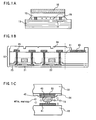
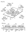
- a semiconductor device of the present invention is manufactured.
- the integrated circuit films 7001 to 7005 are each bonded to a fifth substrate 7010 in which multi-wired layers are formed in both surfaces of a printed board.
- a method for bonding one of the mounting methods described in Embodiment 1 or 2 is used.
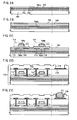
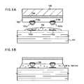
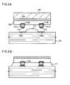
- the process of the manufacturing a semiconductor device it is unnecessary to make the integrated circuit film thinner by grinding a backside thereof, thereby preventing defects from being produced in the back-grinding process and enhancing a process yield.
- the back-grinding process is not required, and therefore, a process of manufacturing a TFT and a process of manufacturing a protruding electrode (bump) can be performed sequentially.
Landscapes
- Thin Film Transistor (AREA)
- Cooling Or The Like Of Semiconductors Or Solid State Devices (AREA)
- Recrystallisation Techniques (AREA)
- Electrodes Of Semiconductors (AREA)
- Internal Circuitry In Semiconductor Integrated Circuit Devices (AREA)
- Wire Bonding (AREA)
- Mechanical Treatment Of Semiconductor (AREA)
- Container, Conveyance, Adherence, Positioning, Of Wafer (AREA)
Applications Claiming Priority (2)
| Application Number | Priority Date | Filing Date | Title |
|---|---|---|---|
| JP2002377816A JP4101643B2 (ja) | 2002-12-26 | 2002-12-26 | 半導体装置の作製方法 |
| JP2002377816 | 2002-12-26 |
Publications (2)
| Publication Number | Publication Date |
|---|---|
| EP1434262A2 true EP1434262A2 (de) | 2004-06-30 |
| EP1434262A3 EP1434262A3 (de) | 2006-09-20 |
Family
ID=32463593
Family Applications (1)
| Application Number | Title | Priority Date | Filing Date |
|---|---|---|---|
| EP03029012A Ceased EP1434262A3 (de) | 2002-12-26 | 2003-12-16 | Halbleiteranordnung hergestellt durch Transfertechnik |
Country Status (6)
| Country | Link |
|---|---|
| US (2) | US7303942B2 (de) |
| EP (1) | EP1434262A3 (de) |
| JP (1) | JP4101643B2 (de) |
| KR (1) | KR101031983B1 (de) |
| CN (1) | CN100505254C (de) |
| TW (1) | TWI330396B (de) |
Families Citing this family (23)
| Publication number | Priority date | Publication date | Assignee | Title |
|---|---|---|---|---|
| JP4554152B2 (ja) * | 2002-12-19 | 2010-09-29 | 株式会社半導体エネルギー研究所 | 半導体チップの作製方法 |
| US7436050B2 (en) | 2003-01-22 | 2008-10-14 | Semiconductor Energy Laboratory Co., Ltd. | Semiconductor device having a flexible printed circuit |
| JP2004247373A (ja) * | 2003-02-12 | 2004-09-02 | Semiconductor Energy Lab Co Ltd | 半導体装置 |
| JP4531341B2 (ja) * | 2003-02-28 | 2010-08-25 | 株式会社半導体エネルギー研究所 | 発光装置および電子機器 |
| JP4526771B2 (ja) | 2003-03-14 | 2010-08-18 | 株式会社半導体エネルギー研究所 | 半導体装置の作製方法 |
| WO2006033451A1 (en) * | 2004-09-24 | 2006-03-30 | Semiconductor Energy Laboratory Co., Ltd. | Semiconductor device and method for manufacturing the same |
| CN101044624A (zh) * | 2004-10-22 | 2007-09-26 | 株式会社半导体能源研究所 | 半导体器件 |
| JP4619186B2 (ja) | 2005-04-19 | 2011-01-26 | 株式会社半導体エネルギー研究所 | 発光装置 |
| US7456104B2 (en) * | 2005-05-31 | 2008-11-25 | Semiconductor Energy Laboratory Co., Ltd. | Semiconductor device and manufacturing method thereof |
| US7719103B2 (en) * | 2005-06-30 | 2010-05-18 | Semiconductor Energy Laboratory Co., Ltd | Semiconductor device |
| JP4926426B2 (ja) | 2005-08-12 | 2012-05-09 | 株式会社半導体エネルギー研究所 | 電子機器 |
| US20080003780A1 (en) * | 2006-06-30 | 2008-01-03 | Haixiao Sun | Detachable stiffener for ultra-thin die |
| US7714535B2 (en) * | 2006-07-28 | 2010-05-11 | Semiconductor Energy Laboratory Co., Ltd. | Power storage device |
| US8232621B2 (en) * | 2006-07-28 | 2012-07-31 | Semiconductor Energy Laboratory Co., Ltd. | Semiconductor device |
| US7648891B2 (en) * | 2006-12-22 | 2010-01-19 | International Business Machines Corporation | Semiconductor chip shape alteration |
| US8110906B2 (en) * | 2007-01-23 | 2012-02-07 | Infineon Technologies Ag | Semiconductor device including isolation layer |
| US7923823B2 (en) * | 2007-01-23 | 2011-04-12 | Infineon Technologies Ag | Semiconductor device with parylene coating |
| FR2943849B1 (fr) * | 2009-03-31 | 2011-08-26 | St Microelectronics Grenoble 2 | Procede de realisation de boitiers semi-conducteurs et boitier semi-conducteur |
| US8598691B2 (en) * | 2011-09-09 | 2013-12-03 | Taiwan Semiconductor Manufacturing Company, Ltd. | Semiconductor devices and methods of manufacturing and packaging thereof |
| US9504168B2 (en) * | 2011-09-30 | 2016-11-22 | Intel Corporation | Fluxing-encapsulant material for microelectronic packages assembled via thermal compression bonding process |
| JP2015156492A (ja) * | 2015-03-05 | 2015-08-27 | セイコーエプソン株式会社 | 半導体回路、転写元基板、転写先基板、半導体回路装置、及び電気光学装置 |
| WO2020046208A1 (en) * | 2018-08-29 | 2020-03-05 | Thales Solutions Asia Pte Ltd | Nanostructure transfer method |
| US12476214B2 (en) | 2021-12-21 | 2025-11-18 | Intel Corporation | Solder interconnect hierarchy for heterogeneous electronic device packaging |
Citations (2)
| Publication number | Priority date | Publication date | Assignee | Title |
|---|---|---|---|---|
| JPH1120360A (ja) * | 1997-07-03 | 1999-01-26 | Seiko Epson Corp | Icカード及び薄膜集積回路装置並びにそれらの製造方法 |
| DE10047963A1 (de) * | 1999-09-28 | 2001-03-29 | Sony Corp | Dünnfilm-Bauteil und Verfahren zu dessen Herstellung |
Family Cites Families (74)
| Publication number | Priority date | Publication date | Assignee | Title |
|---|---|---|---|---|
| US586166A (en) * | 1897-07-13 | Combined automatic fender and brake | ||
| JPS60178424A (ja) | 1984-02-24 | 1985-09-12 | Sharp Corp | 液晶表示素子 |
| JP2816244B2 (ja) | 1990-07-11 | 1998-10-27 | 株式会社日立製作所 | 積層型マルチチップ半導体装置およびこれに用いる半導体装置 |
| US5206749A (en) | 1990-12-31 | 1993-04-27 | Kopin Corporation | Liquid crystal display having essentially single crystal transistors pixels and driving circuits |
| US5376561A (en) | 1990-12-31 | 1994-12-27 | Kopin Corporation | High density electronic circuit modules |
| US6143582A (en) | 1990-12-31 | 2000-11-07 | Kopin Corporation | High density electronic circuit modules |
| US7075501B1 (en) | 1990-12-31 | 2006-07-11 | Kopin Corporation | Head mounted display system |
| US6067082A (en) | 1992-11-09 | 2000-05-23 | Enmei; Toshiharu | Portable communicator |
| JP2953899B2 (ja) | 1993-02-17 | 1999-09-27 | 松下電器産業株式会社 | 半導体装置 |
| US5643804A (en) | 1993-05-21 | 1997-07-01 | Semiconductor Energy Laboratory Co., Ltd. | Method of manufacturing a hybrid integrated circuit component having a laminated body |
| JPH09503622A (ja) | 1993-09-30 | 1997-04-08 | コピン・コーポレーシヨン | 転写薄膜回路を使用した3次元プロセッサー |
| JP2900229B2 (ja) | 1994-12-27 | 1999-06-02 | 株式会社半導体エネルギー研究所 | 半導体装置およびその作製方法および電気光学装置 |
| JP3417110B2 (ja) | 1994-12-30 | 2003-06-16 | カシオ計算機株式会社 | 電子部品の接続方法 |
| JP3364081B2 (ja) | 1995-02-16 | 2003-01-08 | 株式会社半導体エネルギー研究所 | 半導体装置の作製方法 |
| US5757456A (en) | 1995-03-10 | 1998-05-26 | Semiconductor Energy Laboratory Co., Ltd. | Display device and method of fabricating involving peeling circuits from one substrate and mounting on other |
| US5834327A (en) | 1995-03-18 | 1998-11-10 | Semiconductor Energy Laboratory Co., Ltd. | Method for producing display device |
| JP3454965B2 (ja) | 1995-03-22 | 2003-10-06 | 株式会社半導体エネルギー研究所 | 液晶表示装置及びその作製方法 |
| US5861666A (en) | 1995-08-30 | 1999-01-19 | Tessera, Inc. | Stacked chip assembly |
| US6027958A (en) | 1996-07-11 | 2000-02-22 | Kopin Corporation | Transferred flexible integrated circuit |
| JP3809681B2 (ja) | 1996-08-27 | 2006-08-16 | セイコーエプソン株式会社 | 剥離方法 |
| EP1351308B1 (de) | 1996-08-27 | 2009-04-22 | Seiko Epson Corporation | Ablösungsverfahren und Verfahren zum Übertragen eines Dünnfilm-Bauelements |
| JP3809712B2 (ja) | 1996-08-27 | 2006-08-16 | セイコーエプソン株式会社 | 薄膜デバイスの転写方法 |
| JP4619461B2 (ja) | 1996-08-27 | 2011-01-26 | セイコーエプソン株式会社 | 薄膜デバイスの転写方法、及びデバイスの製造方法 |
| JP4619462B2 (ja) | 1996-08-27 | 2011-01-26 | セイコーエプソン株式会社 | 薄膜素子の転写方法 |
| USRE38466E1 (en) | 1996-11-12 | 2004-03-16 | Seiko Epson Corporation | Manufacturing method of active matrix substrate, active matrix substrate and liquid crystal display device |
| US6127199A (en) | 1996-11-12 | 2000-10-03 | Seiko Epson Corporation | Manufacturing method of active matrix substrate, active matrix substrate and liquid crystal display device |
| JP3604248B2 (ja) * | 1997-02-25 | 2004-12-22 | 沖電気工業株式会社 | 半導体装置の製造方法 |
| JPH10270496A (ja) * | 1997-03-27 | 1998-10-09 | Hitachi Ltd | 電子装置、情報処理装置、半導体装置並びに半導体チップの実装方法 |
| US6208521B1 (en) | 1997-05-19 | 2001-03-27 | Nitto Denko Corporation | Film carrier and laminate type mounting structure using same |
| US6388652B1 (en) | 1997-08-20 | 2002-05-14 | Semiconductor Energy Laboratory Co., Ltd. | Electrooptical device |
| CA2218307C (en) | 1997-10-10 | 2006-01-03 | Gennum Corporation | Three dimensional packaging configuration for multi-chip module assembly |
| JP4085459B2 (ja) | 1998-03-02 | 2008-05-14 | セイコーエプソン株式会社 | 3次元デバイスの製造方法 |
| JP3147087B2 (ja) | 1998-06-17 | 2001-03-19 | 日本電気株式会社 | 積層型半導体装置放熱構造 |
| US6423614B1 (en) | 1998-06-30 | 2002-07-23 | Intel Corporation | Method of delaminating a thin film using non-thermal techniques |
| US6153929A (en) | 1998-08-21 | 2000-11-28 | Micron Technology, Inc. | Low profile multi-IC package connector |
| JP2000061785A (ja) | 1998-08-24 | 2000-02-29 | Nitto Denko Corp | 保護シート貼付半導体ウエハ及び半導体ウエハの研削方法 |
| US6255140B1 (en) * | 1998-10-19 | 2001-07-03 | Industrial Technology Research Institute | Flip chip chip-scale package |
| US6312304B1 (en) | 1998-12-15 | 2001-11-06 | E Ink Corporation | Assembly of microencapsulated electronic displays |
| JP4075204B2 (ja) | 1999-04-09 | 2008-04-16 | 松下電器産業株式会社 | 積層型半導体装置 |
| JP3501977B2 (ja) | 1999-05-31 | 2004-03-02 | 株式会社半導体エネルギー研究所 | 半導体装置 |
| TW480722B (en) | 1999-10-12 | 2002-03-21 | Semiconductor Energy Lab | Manufacturing method of electro-optical device |
| US6287891B1 (en) | 2000-04-05 | 2001-09-11 | Hrl Laboratories, Llc | Method for transferring semiconductor device layers to different substrates |
| JP3798220B2 (ja) | 2000-04-07 | 2006-07-19 | シャープ株式会社 | 半導体装置およびそれを用いる液晶モジュール |
| JP3631956B2 (ja) | 2000-05-12 | 2005-03-23 | 富士通株式会社 | 半導体チップの実装方法 |
| TW536836B (en) | 2000-05-22 | 2003-06-11 | Semiconductor Energy Lab | Light emitting device and electrical appliance |
| TW501282B (en) | 2000-06-07 | 2002-09-01 | Semiconductor Energy Lab | Method of manufacturing semiconductor device |
| JP3813797B2 (ja) * | 2000-07-07 | 2006-08-23 | 株式会社ルネサステクノロジ | 半導体装置の製造方法 |
| JP2002025326A (ja) | 2000-07-13 | 2002-01-25 | Seiko Epson Corp | 光源装置、照明装置、液晶装置及び電子機器 |
| JP2002049359A (ja) | 2000-08-02 | 2002-02-15 | Matsushita Electric Ind Co Ltd | アクティブマトリクス液晶表示素子 |
| US6605826B2 (en) | 2000-08-18 | 2003-08-12 | Semiconductor Energy Laboratory Co., Ltd. | Light-emitting device and display device |
| SG148819A1 (en) | 2000-09-14 | 2009-01-29 | Semiconductor Energy Lab | Semiconductor device and manufacturing method thereof |
| US6506681B2 (en) * | 2000-12-06 | 2003-01-14 | Micron Technology, Inc. | Thin flip—chip method |
| US20020098620A1 (en) * | 2001-01-24 | 2002-07-25 | Yi-Chuan Ding | Chip scale package and manufacturing method thereof |
| JP4803884B2 (ja) | 2001-01-31 | 2011-10-26 | キヤノン株式会社 | 薄膜半導体装置の製造方法 |
| JP2002244576A (ja) | 2001-02-21 | 2002-08-30 | Sony Corp | 表示装置の製造方法、表示装置及び液晶表示装置 |
| WO2003003108A1 (en) | 2001-06-29 | 2003-01-09 | Citizen Watch Co., Ltd. | Liquid crystal display panel and its manufacturing method |
| US8415208B2 (en) | 2001-07-16 | 2013-04-09 | Semiconductor Energy Laboratory Co., Ltd. | Semiconductor device and peeling off method and method of manufacturing semiconductor device |
| JP2003109773A (ja) | 2001-07-27 | 2003-04-11 | Semiconductor Energy Lab Co Ltd | 発光装置、半導体装置およびそれらの作製方法 |
| JP5057619B2 (ja) | 2001-08-01 | 2012-10-24 | 株式会社半導体エネルギー研究所 | 半導体装置の作製方法 |
| TW554398B (en) | 2001-08-10 | 2003-09-21 | Semiconductor Energy Lab | Method of peeling off and method of manufacturing semiconductor device |
| US7351300B2 (en) | 2001-08-22 | 2008-04-01 | Semiconductor Energy Laboratory Co., Ltd. | Peeling method and method of manufacturing semiconductor device |
| JP2002189447A (ja) | 2001-10-01 | 2002-07-05 | Canon Inc | エレクトロ・ルミネセンス素子及び装置、並びにその製造法 |
| TW594947B (en) | 2001-10-30 | 2004-06-21 | Semiconductor Energy Lab | Semiconductor device and method of manufacturing the same |
| US6911675B2 (en) | 2001-11-30 | 2005-06-28 | Semiconductor Energy Laboratory Co., Ltd. | Active matrix display device and manufacturing method thereof |
| DE60325669D1 (de) | 2002-05-17 | 2009-02-26 | Semiconductor Energy Lab | Verfahren zum Transferieren eines Objekts und Verfahren zur Herstellung eines Halbleiterbauelements |
| TWI272641B (en) | 2002-07-16 | 2007-02-01 | Semiconductor Energy Lab | Method of manufacturing a semiconductor device |
| US7087458B2 (en) * | 2002-10-30 | 2006-08-08 | Advanpack Solutions Pte. Ltd. | Method for fabricating a flip chip package with pillar bump and no flow underfill |
| KR101079757B1 (ko) | 2002-10-30 | 2011-11-04 | 가부시키가이샤 한도오따이 에네루기 켄큐쇼 | 반도체장치 및 반도체장치의 제작방법 |
| US6818850B2 (en) | 2002-11-07 | 2004-11-16 | Bridges Electric, Inc. | Disconnect switch for switching capacitive currents |
| US7056810B2 (en) | 2002-12-18 | 2006-06-06 | Semiconductor Energy Laboratory Co., Ltd. | Method for manufacturing semiconductor apparatus, and semiconductor apparatus and electric appliance |
| JP4554152B2 (ja) | 2002-12-19 | 2010-09-29 | 株式会社半導体エネルギー研究所 | 半導体チップの作製方法 |
| US7436050B2 (en) | 2003-01-22 | 2008-10-14 | Semiconductor Energy Laboratory Co., Ltd. | Semiconductor device having a flexible printed circuit |
| JP2004247373A (ja) | 2003-02-12 | 2004-09-02 | Semiconductor Energy Lab Co Ltd | 半導体装置 |
| JP4526771B2 (ja) | 2003-03-14 | 2010-08-18 | 株式会社半導体エネルギー研究所 | 半導体装置の作製方法 |
-
2002
- 2002-12-26 JP JP2002377816A patent/JP4101643B2/ja not_active Expired - Fee Related
-
2003
- 2003-12-16 EP EP03029012A patent/EP1434262A3/de not_active Ceased
- 2003-12-16 US US10/735,767 patent/US7303942B2/en not_active Expired - Lifetime
- 2003-12-19 TW TW092136231A patent/TWI330396B/zh not_active IP Right Cessation
- 2003-12-24 KR KR1020030096060A patent/KR101031983B1/ko not_active Expired - Fee Related
- 2003-12-26 CN CNB2003101235580A patent/CN100505254C/zh not_active Expired - Fee Related
-
2007
- 2007-11-30 US US11/947,835 patent/US7564139B2/en not_active Expired - Fee Related
Patent Citations (2)
| Publication number | Priority date | Publication date | Assignee | Title |
|---|---|---|---|---|
| JPH1120360A (ja) * | 1997-07-03 | 1999-01-26 | Seiko Epson Corp | Icカード及び薄膜集積回路装置並びにそれらの製造方法 |
| DE10047963A1 (de) * | 1999-09-28 | 2001-03-29 | Sony Corp | Dünnfilm-Bauteil und Verfahren zu dessen Herstellung |
Non-Patent Citations (1)
| Title |
|---|
| XIANG ZHANG ET AL: "THERMAL CONDUCTIVITY AND DIFFUSIVITY OF FREE-STANDING SILICON NITRIDE THIN FILMS", REVIEW OF SCIENTIFIC INSTRUMENTS, AIP, MELVILLE, NY, US, vol. 66, no. 2, PART 01, 1 February 1995 (1995-02-01), pages 1115 - 1120, XP000503532, ISSN: 0034-6748, DOI: 10.1063/1.1145989 * |
Also Published As
| Publication number | Publication date |
|---|---|
| CN1519933A (zh) | 2004-08-11 |
| JP2004207652A (ja) | 2004-07-22 |
| US7564139B2 (en) | 2009-07-21 |
| US20040124542A1 (en) | 2004-07-01 |
| TW200414401A (en) | 2004-08-01 |
| US20080088034A1 (en) | 2008-04-17 |
| KR20040057999A (ko) | 2004-07-02 |
| EP1434262A3 (de) | 2006-09-20 |
| KR101031983B1 (ko) | 2011-05-02 |
| JP4101643B2 (ja) | 2008-06-18 |
| CN100505254C (zh) | 2009-06-24 |
| US7303942B2 (en) | 2007-12-04 |
| TWI330396B (en) | 2010-09-11 |
Similar Documents
| Publication | Publication Date | Title |
|---|---|---|
| US7564139B2 (en) | Semiconductor device and method for manufacturing the same | |
| KR101013482B1 (ko) | 반도체 장치 및 그의 제작방법 | |
| JP6549272B2 (ja) | 半導体装置の作製方法 | |
| JP4027740B2 (ja) | 半導体装置の作製方法 | |
| EP1383165B1 (de) | Methode zur Herstellung eines Halbleiterbauelementes | |
| KR101158831B1 (ko) | 반도체 칩 및 그 제조방법 | |
| KR100993130B1 (ko) | 반도체 장치 제작 방법 | |
| US20110159771A1 (en) | Semiconductor device and manufacturing method thereof | |
| JP4567282B2 (ja) | 発光装置の作製方法 | |
| JP4527068B2 (ja) | 剥離方法、半導体装置の作製方法、及び電子書籍の作製方法 | |
| EP1439577B1 (de) | Halbleiteranordnung und Herstellungsverfahren dafür | |
| JP4267394B2 (ja) | 剥離方法、及び半導体装置の作製方法 | |
| JP4602035B2 (ja) | 半導体装置の作製方法 | |
| JP2005056985A (ja) | 半導体装置の製造方法、半導体装置および電子機器 |
Legal Events
| Date | Code | Title | Description |
|---|---|---|---|
| PUAI | Public reference made under article 153(3) epc to a published international application that has entered the european phase |
Free format text: ORIGINAL CODE: 0009012 |
|
| AK | Designated contracting states |
Kind code of ref document: A2 Designated state(s): AT BE BG CH CY CZ DE DK EE ES FI FR GB GR HU IE IT LI LU MC NL PT RO SE SI SK TR |
|
| AX | Request for extension of the european patent |
Extension state: AL LT LV MK |
|
| PUAL | Search report despatched |
Free format text: ORIGINAL CODE: 0009013 |
|
| AK | Designated contracting states |
Kind code of ref document: A3 Designated state(s): AT BE BG CH CY CZ DE DK EE ES FI FR GB GR HU IE IT LI LU MC NL PT RO SE SI SK TR |
|
| AX | Request for extension of the european patent |
Extension state: AL LT LV MK |
|
| 17P | Request for examination filed |
Effective date: 20070314 |
|
| AKX | Designation fees paid |
Designated state(s): DE FI FR GB NL |
|
| 17Q | First examination report despatched |
Effective date: 20170208 |
|
| STAA | Information on the status of an ep patent application or granted ep patent |
Free format text: STATUS: THE APPLICATION HAS BEEN REFUSED |
|
| 18R | Application refused |
Effective date: 20181113 |