EP1434195B1 - Image processing apparatus, image transmission apparatus, image reception apparatus, and image processing method - Google Patents
Image processing apparatus, image transmission apparatus, image reception apparatus, and image processing method Download PDFInfo
- Publication number
- EP1434195B1 EP1434195B1 EP20020765487 EP02765487A EP1434195B1 EP 1434195 B1 EP1434195 B1 EP 1434195B1 EP 20020765487 EP20020765487 EP 20020765487 EP 02765487 A EP02765487 A EP 02765487A EP 1434195 B1 EP1434195 B1 EP 1434195B1
- Authority
- EP
- European Patent Office
- Prior art keywords
- image
- bit
- image processing
- plane number
- raster
- Prior art date
- Legal status (The legal status is an assumption and is not a legal conclusion. Google has not performed a legal analysis and makes no representation as to the accuracy of the status listed.)
- Expired - Lifetime
Links
- 230000005540 biological transmission Effects 0.000 title claims description 75
- 238000003672 processing method Methods 0.000 title claims description 43
- 239000011159 matrix material Substances 0.000 claims description 59
- 230000009467 reduction Effects 0.000 claims description 24
- 239000000758 substrate Substances 0.000 claims description 15
- 238000010586 diagram Methods 0.000 description 47
- 238000000034 method Methods 0.000 description 34
- 238000007906 compression Methods 0.000 description 25
- 230000006835 compression Effects 0.000 description 23
- 238000010276 construction Methods 0.000 description 23
- 238000006243 chemical reaction Methods 0.000 description 14
- 230000006837 decompression Effects 0.000 description 14
- 230000000694 effects Effects 0.000 description 14
- 239000003086 colorant Substances 0.000 description 13
- 239000004973 liquid crystal related substance Substances 0.000 description 9
- 230000008569 process Effects 0.000 description 8
- 239000010409 thin film Substances 0.000 description 8
- 230000006866 deterioration Effects 0.000 description 7
- 239000002131 composite material Substances 0.000 description 6
- 239000011521 glass Substances 0.000 description 5
- 230000007704 transition Effects 0.000 description 4
- 230000008859 change Effects 0.000 description 3
- 238000013144 data compression Methods 0.000 description 3
- 238000004364 calculation method Methods 0.000 description 2
- 238000012986 modification Methods 0.000 description 2
- 230000004048 modification Effects 0.000 description 2
- 229910021420 polycrystalline silicon Inorganic materials 0.000 description 2
- 229920005591 polysilicon Polymers 0.000 description 2
- 101150018075 sel-2 gene Proteins 0.000 description 2
- 239000002699 waste material Substances 0.000 description 2
- 238000003491 array Methods 0.000 description 1
- 125000004122 cyclic group Chemical group 0.000 description 1
- 230000002542 deteriorative effect Effects 0.000 description 1
- 238000005516 engineering process Methods 0.000 description 1
- 230000006870 function Effects 0.000 description 1
- 238000013139 quantization Methods 0.000 description 1
- 230000005236 sound signal Effects 0.000 description 1
Images


Classifications
-
- G—PHYSICS
- G09—EDUCATION; CRYPTOGRAPHY; DISPLAY; ADVERTISING; SEALS
- G09G—ARRANGEMENTS OR CIRCUITS FOR CONTROL OF INDICATING DEVICES USING STATIC MEANS TO PRESENT VARIABLE INFORMATION
- G09G5/00—Control arrangements or circuits for visual indicators common to cathode-ray tube indicators and other visual indicators
- G09G5/02—Control arrangements or circuits for visual indicators common to cathode-ray tube indicators and other visual indicators characterised by the way in which colour is displayed
-
- G—PHYSICS
- G09—EDUCATION; CRYPTOGRAPHY; DISPLAY; ADVERTISING; SEALS
- G09G—ARRANGEMENTS OR CIRCUITS FOR CONTROL OF INDICATING DEVICES USING STATIC MEANS TO PRESENT VARIABLE INFORMATION
- G09G3/00—Control arrangements or circuits, of interest only in connection with visual indicators other than cathode-ray tubes
- G09G3/20—Control arrangements or circuits, of interest only in connection with visual indicators other than cathode-ray tubes for presentation of an assembly of a number of characters, e.g. a page, by composing the assembly by combination of individual elements arranged in a matrix no fixed position being assigned to or needed to be assigned to the individual characters or partial characters
- G09G3/34—Control arrangements or circuits, of interest only in connection with visual indicators other than cathode-ray tubes for presentation of an assembly of a number of characters, e.g. a page, by composing the assembly by combination of individual elements arranged in a matrix no fixed position being assigned to or needed to be assigned to the individual characters or partial characters by control of light from an independent source
- G09G3/36—Control arrangements or circuits, of interest only in connection with visual indicators other than cathode-ray tubes for presentation of an assembly of a number of characters, e.g. a page, by composing the assembly by combination of individual elements arranged in a matrix no fixed position being assigned to or needed to be assigned to the individual characters or partial characters by control of light from an independent source using liquid crystals
- G09G3/3611—Control of matrices with row and column drivers
- G09G3/3685—Details of drivers for data electrodes
- G09G3/3688—Details of drivers for data electrodes suitable for active matrices only
-
- H—ELECTRICITY
- H04—ELECTRIC COMMUNICATION TECHNIQUE
- H04N—PICTORIAL COMMUNICATION, e.g. TELEVISION
- H04N19/00—Methods or arrangements for coding, decoding, compressing or decompressing digital video signals
- H04N19/10—Methods or arrangements for coding, decoding, compressing or decompressing digital video signals using adaptive coding
- H04N19/169—Methods or arrangements for coding, decoding, compressing or decompressing digital video signals using adaptive coding characterised by the coding unit, i.e. the structural portion or semantic portion of the video signal being the object or the subject of the adaptive coding
- H04N19/184—Methods or arrangements for coding, decoding, compressing or decompressing digital video signals using adaptive coding characterised by the coding unit, i.e. the structural portion or semantic portion of the video signal being the object or the subject of the adaptive coding the unit being bits, e.g. of the compressed video stream
-
- H—ELECTRICITY
- H04—ELECTRIC COMMUNICATION TECHNIQUE
- H04N—PICTORIAL COMMUNICATION, e.g. TELEVISION
- H04N19/00—Methods or arrangements for coding, decoding, compressing or decompressing digital video signals
- H04N19/42—Methods or arrangements for coding, decoding, compressing or decompressing digital video signals characterised by implementation details or hardware specially adapted for video compression or decompression, e.g. dedicated software implementation
- H04N19/423—Methods or arrangements for coding, decoding, compressing or decompressing digital video signals characterised by implementation details or hardware specially adapted for video compression or decompression, e.g. dedicated software implementation characterised by memory arrangements
- H04N19/426—Methods or arrangements for coding, decoding, compressing or decompressing digital video signals characterised by implementation details or hardware specially adapted for video compression or decompression, e.g. dedicated software implementation characterised by memory arrangements using memory downsizing methods
-
- H—ELECTRICITY
- H04—ELECTRIC COMMUNICATION TECHNIQUE
- H04N—PICTORIAL COMMUNICATION, e.g. TELEVISION
- H04N19/00—Methods or arrangements for coding, decoding, compressing or decompressing digital video signals
- H04N19/50—Methods or arrangements for coding, decoding, compressing or decompressing digital video signals using predictive coding
- H04N19/59—Methods or arrangements for coding, decoding, compressing or decompressing digital video signals using predictive coding involving spatial sub-sampling or interpolation, e.g. alteration of picture size or resolution
-
- G—PHYSICS
- G09—EDUCATION; CRYPTOGRAPHY; DISPLAY; ADVERTISING; SEALS
- G09G—ARRANGEMENTS OR CIRCUITS FOR CONTROL OF INDICATING DEVICES USING STATIC MEANS TO PRESENT VARIABLE INFORMATION
- G09G2300/00—Aspects of the constitution of display devices
- G09G2300/04—Structural and physical details of display devices
- G09G2300/0404—Matrix technologies
- G09G2300/0408—Integration of the drivers onto the display substrate
-
- G—PHYSICS
- G09—EDUCATION; CRYPTOGRAPHY; DISPLAY; ADVERTISING; SEALS
- G09G—ARRANGEMENTS OR CIRCUITS FOR CONTROL OF INDICATING DEVICES USING STATIC MEANS TO PRESENT VARIABLE INFORMATION
- G09G2310/00—Command of the display device
- G09G2310/02—Addressing, scanning or driving the display screen or processing steps related thereto
- G09G2310/0264—Details of driving circuits
- G09G2310/027—Details of drivers for data electrodes, the drivers handling digital grey scale data, e.g. use of D/A converters
-
- G—PHYSICS
- G09—EDUCATION; CRYPTOGRAPHY; DISPLAY; ADVERTISING; SEALS
- G09G—ARRANGEMENTS OR CIRCUITS FOR CONTROL OF INDICATING DEVICES USING STATIC MEANS TO PRESENT VARIABLE INFORMATION
- G09G2330/00—Aspects of power supply; Aspects of display protection and defect management
- G09G2330/02—Details of power systems and of start or stop of display operation
- G09G2330/021—Power management, e.g. power saving
-
- G—PHYSICS
- G09—EDUCATION; CRYPTOGRAPHY; DISPLAY; ADVERTISING; SEALS
- G09G—ARRANGEMENTS OR CIRCUITS FOR CONTROL OF INDICATING DEVICES USING STATIC MEANS TO PRESENT VARIABLE INFORMATION
- G09G2340/00—Aspects of display data processing
- G09G2340/02—Handling of images in compressed format, e.g. JPEG, MPEG
-
- G—PHYSICS
- G09—EDUCATION; CRYPTOGRAPHY; DISPLAY; ADVERTISING; SEALS
- G09G—ARRANGEMENTS OR CIRCUITS FOR CONTROL OF INDICATING DEVICES USING STATIC MEANS TO PRESENT VARIABLE INFORMATION
- G09G2340/00—Aspects of display data processing
- G09G2340/04—Changes in size, position or resolution of an image
- G09G2340/0407—Resolution change, inclusive of the use of different resolutions for different screen areas
- G09G2340/0428—Gradation resolution change
-
- G—PHYSICS
- G09—EDUCATION; CRYPTOGRAPHY; DISPLAY; ADVERTISING; SEALS
- G09G—ARRANGEMENTS OR CIRCUITS FOR CONTROL OF INDICATING DEVICES USING STATIC MEANS TO PRESENT VARIABLE INFORMATION
- G09G2360/00—Aspects of the architecture of display systems
- G09G2360/18—Use of a frame buffer in a display terminal, inclusive of the display panel
-
- G—PHYSICS
- G09—EDUCATION; CRYPTOGRAPHY; DISPLAY; ADVERTISING; SEALS
- G09G—ARRANGEMENTS OR CIRCUITS FOR CONTROL OF INDICATING DEVICES USING STATIC MEANS TO PRESENT VARIABLE INFORMATION
- G09G3/00—Control arrangements or circuits, of interest only in connection with visual indicators other than cathode-ray tubes
- G09G3/20—Control arrangements or circuits, of interest only in connection with visual indicators other than cathode-ray tubes for presentation of an assembly of a number of characters, e.g. a page, by composing the assembly by combination of individual elements arranged in a matrix no fixed position being assigned to or needed to be assigned to the individual characters or partial characters
- G09G3/2007—Display of intermediate tones
- G09G3/2044—Display of intermediate tones using dithering
- G09G3/2051—Display of intermediate tones using dithering with use of a spatial dither pattern
-
- G—PHYSICS
- G09—EDUCATION; CRYPTOGRAPHY; DISPLAY; ADVERTISING; SEALS
- G09G—ARRANGEMENTS OR CIRCUITS FOR CONTROL OF INDICATING DEVICES USING STATIC MEANS TO PRESENT VARIABLE INFORMATION
- G09G5/00—Control arrangements or circuits for visual indicators common to cathode-ray tube indicators and other visual indicators
- G09G5/003—Details of a display terminal, the details relating to the control arrangement of the display terminal and to the interfaces thereto
- G09G5/006—Details of the interface to the display terminal
Definitions
- the present invention relates to an image processing apparatus, an image transmission apparatus and an image processing method, and more specifically to an image processing apparatus, an image transmission apparatus and an image processing method for achieving high quality images in image processing by a display having a memory which stores raster images as well as improving efficiency in the transmission of raster images from a computer to the display.
- an image may be compressed into a file format such as JPEG and GIF, and then transmitted.
- a processor which executes high-speed operations for compressing and decompressing the image with respect to each frame, thereby resulting in an increase in costs.
- a display may be provided with a built-in frame memory which serves as a memory for storing a raster image to suspend the transmission of data when a still image is being displayed.
- This measure is effective especially for mobile information equipment and the like since it is also possible to reduce electric power consumption.
- Reductions in electric power consumption and chip size are important for the display which is installed in mobile information equipment. Accordingly, it is desirable that an image stored in a memory should be displayed when displaying a still image, and that the capacity or size of the memory, which occupies a large proportion of chip size, should be small.
- the reduced demand of memory capacity means that chip size can be reduced.
- image data may be compressed.
- a graphical data compression method utilizing a format such as JPEG and GIF, it is required to have an image processor for decompressing images, which counteracts the effect of reducing electric power consumption and chip size.
- bit-plane number means the number n of bits of data representing the tone or gray level of a digital image which has been quantized by 2 n .
- the methods for reducing the bit-plane number include the multi-valued dither method and the fixed threshold method. Details regarding these methods are described in " The New Image Electron Handbook" (Tokyo, Corona Publishing Co. Ltd., 1993), pp. 41 - 51 .
- the multi-valued dither method and the fixed threshold method are different from the graphical data compression method utilizing a format such as JPEG and GIF in that compressed images do not require decompression.
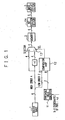
- Fig. 1 is a block diagram schematically showing the configuration of a conventional image processing apparatus.
- a description will be given of an example of bit-plane compression of a raster image by the conventional multi-valued dither method, in which an RGB raster image with 6 bits per color component is transmitted from a computer, and an image display section displays an image with 6 bits per color component.
- a threshold value generator 11 generates a dither matrix based on ordered dithering, and outputs a 2-bit value, which is uniquely determined according to the pixel (X-Y coordinate values) of an input image, to the comparator 12.
- the comparator 12 compares the low order 2 bits sent from the raster image 1 with the 2-bit value from the threshold value generator 11. When the value received from the threshold value generator 11 is larger than the low order 2 bits, the comparator 12 outputs "1" to a selector 13. Otherwise, the comparator 12 outputs "0" to the selector 13.
- the selector 13 outputs high order or most significant 4 bits of the raster image 1 directly or a value obtained by subtracting 1 therefrom to a memory 2 based on the output value from the comparator 12. For an image with 4 bits per color component stored in the memory 2, the value of high order 2 bits of the 4 bits is attached as low order bits to the input 4-bit value by a bit addition section 14, and the image is output to an image display section 3 as a 6-bit image.
- bit-plane number is reduced by the multi-valued dither method, and a pseudo image with 6 bits per color component is displayed.
- Japanese Patent Publication No. HEI2-8493(B ) (first prior art) has disclosed a digital signal processing apparatus which performs level-compression of a digitized input signal to transmit the signal and level-decompression of a compressed signal transmitted thereto, comprising circuits for detecting a maximum value of a digital signal, performing level-compression after adding a dither value to the digital signal based on the maximum value, performing level-decompression and subtracting the dither value from the digital signal, respectively.
- US-A-5 553 200 discloses an apparatus and a method for providing bit-rate reduction and reconstruction of image data. In particular, it discloses a method of providing bit-rate reduction and reconstruction of image data using dither arrays. It simply teaches encoding 32-bit CMYK combinations into either 16-bit or 8-bit code words on a pixel by pixel basis by either stepwise calculations or by using look-up tables. Further, US-A-5 553 200 teaches thresholding a normalized pixel offset value I" (i, j) against a corresponding value from a dither array and coding the pixel value. Then, it teaches reconstructing the coded information by "using a look-up table". Figure 6 in US-A-5 553 200 presents a sample of the "look-up table”. That is, it teaches using a look-up table to reconstruct encoded pixel values.
- the reduction of the bit-plane number causes pseudo outlines and pseudo colors, and produces a grainy picture.
- the quality of an image is deteriorated.
- superimpose This is a technique for superimposing a different image such as "text" on a display screen image.
- a plurality of images e.g. a picture or a graphic and text
- a transmission bus which has a limitation in bus width.
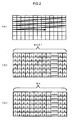
- Fig. 2 (a) when displaying an image on a display device, etc., an image signal is input to each pixel along a main scanning line as well as a sub scanning line, and this operation is repeated with respect to a plurality of lines so that the image signal can be input to all the pixels.
- a dither period is set to 4 bits.
- Fig. 2 (b) when the number of pixels in the main scanning direction of a display is 4n + 1, dither periodicity appears in both main scanning direction and sub scanning direction, and therefore compression and decompression of an image cause less deterioration in picture quality.
- the number of pixels in the main scanning direction of a display is 4n + 2 or 4n + 3. That is, in the case where the number of pixels in the main scanning direction of a display does not include the dither period as a factor, compression and decompression of an image cause less deterioration in picture quality.
- dither processing for a raster image
- the number of pixels in the main scanning direction of a display is generally a number including "2" to "6" as a factor (e.g. 480, 720, 840, etc.). Therefore, when applying the first prior art to image display, dither periodicity is not observed in sub scanning direction, while it appears in main scanning direction as can be seen in Fig. 2 (c) . Thus, picture quality deteriorates with compression and decompression of an image.
- the dither period is set to a larger value so as not to be a factor of the number of pixels in the main scanning direction of a display, a high-frequency minimal noise, the intended purpose of dither processing, cannot be achieved. Thus, picture quality deteriorates with compression and decompression of an image.
- the first prior art is directly used, it is required to have a maximum value detecting circuit on a compression side for specifying a bit of a digital signal, which is formed of a plurality of bits, to which a dither value is to be added, and also transmit a signal indicating the place of the most utilized bit of a maximum value with a digital signal as needed.
- the signal that indicates the place of the most utilized bit has to be stored in the memory together with the digital signal.
- the construction for executing such processing needs intricate circuitry, which increases electric power consumption and chip size. Therefore, this construction is not suitable for an image processing apparatus such as a display.
- the first prior art does not teach or suggest the processing method with respect to the maximum value and the minimum value of a digital signal. Consequently, in an image processing apparatus which often provides a "white” or the maximum value display and a "black” or the minimum value display (e.g. text output, geometrical configuration display, etc), picture quality deteriorates. This is because a grainy picture is often produced on the occasion of the "black” and "white” display.
- an image processing apparatus comprising a first image processing means for reducing the bit-plane number of a raster image, which is an original image, and a second image processing means for increasing the bit-plane number.
- the image processing apparatus is an image processing apparatus that reduces the bit-plane number of a raster image, which is an original image, and after that, increases the reduced bit-plane number of the raster image to the number equal to or less than the bit-plane number of the original image, comprising: a first image processing means for performing multi-valued dither processing with the use of a two-dimensional dither matrix when reducing the bit-plane number of the raster image; and a second image processing means for performing bit addition processing based on the two-dimensional dither matrix used by the first image processing means and the gray level of the raster image whose bit-plane number has been reduced when increasing the reduced bit-plane number of the raster image.
- It preferably comprises: a first image processing means for performing multi-valued dither processing with the use of a two-dimensional dither matrix when reducing the bit-plane number of the raster image; and a second image processing means for performing frame rate control processing to periodically change tones based on the two-dimensional dither matrix used by the first image processing means when increasing the reduced bit-plane number of the raster image.
- the second image processing means preferably further adds an offset value in order that the difference between the signal value of the original image and the average of all the dither values of the raster image whose bit-plane number has been increased will be the minimum.
- the raster image whose bit-plane number has been reduced is transmitted via a transmission bus having a bus width less than the bit-plane number of the original image.
- the image processing apparatus should further comprise a storage for storing data of the raster image whose bit-plane number has been reduced by the first image processing means, and the second image processing means should read out the data of the raster image stored in the storage to increase its bit-plane number.
- the second image processing means is preferably formed on the substrate where the drive circuit of a display is formed.
- the first image processing means is preferably formed on the substrate where the drive circuit of the display is formed.
- the first image processing means reduces the bit-plane number of a raster image, which is an original image, and after that, the second image processing means increases the reduced bit-plane number.
- the second image processing means increases the reduced bit-plane number.
- multi-valued dither processing is performed with the use of a two-dimensional dither matrix when reducing the bit-plane number of a raster image, and bit addition processing is performed based on the two-dimensional dither matrix which has been used for the multi-valued dither processing when increasing the reduced bit-plane number of the raster image. Consequently, there is a smaller difference between the image which has undergone the bit addition processing and the original image as compared to the multi-valued dither method. Thereby, it is possible to suppress a grainy feeling and pseudo colors seen in the case where there is a large difference between the two images, and realize high quality image display.
- the image processing apparatus can be formed on the substrate by the same process. Therefore, the application of the image processing apparatus of the third aspect enables reductions in the memory area and electric power consumption.
- the first and second image processing means perform the image processing in a manner such that the maximum value and minimum value of components of the raster image after the image processing are the same as before.
- the second image processing means is preferably formed on the substrate where the drive circuit of a display is formed.
- the first image processing means is preferably formed on the substrate where the drive circuit of the display is formed.
- an image transmission apparatus for improving the capacity of transmission.
- the image transmission apparatus is the following image transmission apparatuses 2-1 or 2-2.
- the first and second units perform the processing in a manner such that the maximum value and minimum value of components of the raster image after the processing are the same as before.
- the first unit reduces the bit-plane number of an original image, and transmits the raster image whose bit-plane number has been reduced to the second unit
- the second unit increases the bit-plane number of the raster image transmitted from the first unit to the number equal to or less than the bit-plane number of the original image.
- multi-valued dither processing is performed with the use of a two-dimensional dither matrix for a raster image, which is an original image, so as to transmit the raster image whose bit-plane number has been reduced, and after that, bit addition processing is performed based on the two-dimensional dither matrix used for the multi-valued dither processing so that the bit-plane number of the raster image matches the bit-plane number of the original image.
- bit addition processing is performed based on the two-dimensional dither matrix used for the multi-valued dither processing so that the bit-plane number of the raster image matches the bit-plane number of the original image.
- an image reception apparatus which receives a raster image whose bit-plane number has been reduced to less than that of an original image, and increases the bit-plane number of the received image.
- the image reception apparatus is the following image reception apparatuses 3-1 or 3-2.
- the processing is performed in a manner such that the maximum value and minimum value of components of the raster image after the processing are the same as before.
- the image reception apparatus receives a raster image whose bit-plane number has been reduced to less than that of an original image by multi-valued dither processing with the use of a two-dimensional dither matrix, and after that, the image reception apparatus performs bit addition processing based on the two-dimensional dither matrix used for the multi-valued dither processing so that the bit-plane number of the received image matches the bit-plane number of the original image.
- the image reception apparatus performs bit addition processing based on the two-dimensional dither matrix used for the multi-valued dither processing so that the bit-plane number of the received image matches the bit-plane number of the original image.
- an apparatus which is provided with a transmission bus for receiving images having a bus width of only 16 bits, receives a raster image with 6 bits per color component (18 bits in total), the apparatus receives the raster image whose bit-plane number has been reduced at the sending end, and increases the bit-plane number of the received image. Thereby, the apparatus can receive the respective color components of the image comparable in quality to the original image in parallel.
- an image processing method comprising a first image processing step for reducing the bit-plane number of a raster image, which is an original image, and a second image processing step for increasing the bit-plane number of the raster image.
- the image processing method according to the fourth aspect of the present invention is one selected from the following image processing methods 4-1 to 4-3.
- the raster image whose bit-plane number has been reduced is transmitted via a transmission bus having a bus width less than the bit-plane number of the original image.
- the image processing method should further comprise a step for storing the first raster image whose bit-plane number has been reduced at the first image processing step in a storage after the first image processing step, and the raster image stored in the storage should be read out to increase its bit-plane number at the second image processing step.
- the bit-plane number of a raster image which is an original image, is reduced at the first image processing step, and after that, the reduced bit-plane number is increased at the second image processing step.
- multi-valued dither processing is performed with the use of a two-dimensional dither matrix when reducing the bit-plane number of a raster image, and bit addition processing is performed based on the two-dimensional dither matrix which has been used for the multi-valued dither processing when increasing the reduced bit-plane number of the raster image. Consequently, there is a smaller difference between the image which has undergone the bit addition processing and the original image as compared to the multi-valued dither method. Thereby, it is possible to suppress a grainy feeling and pseudo colors seen in the case where there is a large difference between the two images, and realize high quality image display.
- an image processing method by which data for displaying an input image is stored in a storage, and the image is displayed on a prescribed display based on the data read out of the storage, comprising: a first image processing step for compressing at least one layer of a first raster image to produce a compressed layer(s) when the amount of data of a signal for displaying the first raster image, which has been divided into two or more layers when input, exceeds the capacity of the storage; a step for storing the compressed layer(s) and uncompressed layer(s) of the first raster image in the storage; a second image processing step for reading out the compressed layer(s) stored in the storage to decompress the compressed layer(s), and combining the decompressed layer(s) with the uncompressed layer(s) of the first raster image read out of the storage to generate a signal for displaying a second raster image; and a step for outputting the signal for displaying the
- the aforementioned image processing method should further comprise a selecting step before the first image processing step for determining whether to store the signal in the storage without compression or to store the signal in the storage after compressing at least one layer when the amount of data of a signal for displaying the first raster image is within the capacity of the storage, and, in the case where it has been determined at the selecting step that at least one layer is to be compressed, the image processing is also carried out for the first raster image with the amount of data within the capacity of the storage at the first image processing step.
- the image processing method further comprises an output switching step for selecting either a signal for displaying the first raster image or a signal for displaying the second raster image on the display to output the selected signal at the beginning, and, more preferably, further comprises a processing stopping step after the output switching step for stopping the image processing of the first image processing step and the second image processing step when the first raster image is selected at the output switching step.
- the image processing is performed so that the maximum value and minimum value of components of the second raster image match those of the first raster image, respectively, at the first and second image processing steps.
- At least one layer of an original image is compressed and decompressed in the case where a raster image, which has been divided into two or more layers when input, cannot be stored in the storage in its original form. Therefore, an input original image can be stored in the storage regardless of the amount of data or the size of the original image. That is, an apparatus that employs the image processing method of the fifth aspect of the present invention can produce the second raster image and output the image to the display regardless of the amount of data of the original image.
- the image processing method of the fifth aspect when the image processing method of the fifth aspect is applied to the display for image processing, it is possible to provide a superimpose display without requiring more memory capacity by compressing and decompressing a natural image by 1 bit and using the obtained 1 bit for text information.
- an image processing method applied to an image transmission apparatus in which a raster image being an original image is transmitted from a first unit to a second unit comprising: a first image processing step for performing multi-valued dither processing by the first unit with the use of a two-dimensional dither matrix for the raster image, which is an original image; a transmitting step for transmitting the raster image whose bit-plane number has been reduced at the first image processing step to the second unit; and the second image processing step for performing bit addition processing by the second unit based on the two-dimensional dither matrix used for the multi-valued dither processing and the gray level of the raster image whose bit-plane number has been reduced so that the bit-plane number of the raster image transmitted from the first unit matches the bit-plane number of the original image.
- the raster image whose bit-plane number has been reduced is transmitted at the transmitting step.
- multi-valued dither processing is performed with the use of a two-dimensional dither matrix for a raster image, which is an original image, so as to transmit the raster image whose bit-plane number has been reduced, and after that, bit addition processing is performed based on the two-dimensional dither matrix used for the multi-valued dither processing so that the bit-plane number of the raster image matches the bit-plane number of the original image.
- bit addition processing is performed based on the two-dimensional dither matrix used for the multi-valued dither processing so that the bit-plane number of the raster image matches the bit-plane number of the original image.
- the reference numeral 1 represents a raster image.
- the reference numeral 1A represents a raster image (image).
- the reference numeral 1B represents a raster image (text information).
- the reference numeral 2 represents a memory for storing display images.
- the reference numerals 3 and 3A represent image display sections.
- the reference numeral 4 represents an image processing former stage.
- the reference numeral 4A represents a compressor.
- the reference numeral 5 represents an image processing latter stage.
- the reference numeral 5A represents a decompressor.
- the reference numeral 6 represents a memory use switch controller.
- the reference numeral 7 represents a raster image transmitting end (a first unit).
- the reference numeral 8 represents a raster image receiving end (a second unit).
- the reference numeral 9 represents an FRC image processing latter stage.
- the reference numeral 10 represents a liquid crystal display section.
- the reference numerals 11, 11A and 11B represent threshold value generators.
- the reference numeral 12 represents a comparator.
- the reference numerals 13, 13A, 13B, 13C, 13D and 51 represent selectors.
- the reference numerals 14 and 14A represent bit addition sections.
- the reference numerals 15 and 52 represent demultiplexers.
- the reference numeral 16 represents an input/ output switch controller.
- the reference numeral 17 represents an adder.
- the reference numeral 18 represents a quantizer.
- the reference numeral 19 represents a counter.
- the reference numeral 20 represents a carry generator.
- the reference numerals 21A and 21B represent sift registers.
- the reference numeral 22 represents a data register.
- the reference numeral 23 represents a latch.
- the reference numeral 24 represents a D/ A converter.
- the reference numeral 25 represents a data line selector.
- the reference numeral 26 represents a memory controller.
- the reference numeral 27 represents a memory input signal switch controller.
- the reference numeral 28 represents an image compositor.
- the reference numeral 29 represents a control signal.
- the reference numeral 31 represents a picture element (pixel).
- the reference numeral 32 represents a thin film transistor.
- the reference numeral 33 represents a data line.
- the reference numeral 34 represents a gate line.
- the reference numeral 50 represents a bit-plane number reduction controller.
- a 6-bit signal is converted into a 4-bit signal by multi-valued dither processing, and then the 4-bit signal is expanded into a 6-bit signal.
- a dither matrix used in the multi-valued dither processing is based on an ordered dithering
- 6 - 4 2 bits of dither need to be added. Therefore, any of dither components or numbers expressed in binary form, 00, 01, 10, and 11 is added to an input signal.
- the division by 4 is corresponding to the conversion from 6 bits to 4 bits.
- an input signal value is, for example, 37 (100101 in binary form)
- it is converted into 9 (1001) by the multi-valued dither processing when the dither component is 00, into 9 (1001) when the dither component is 01, into 8 (1000) when the dither component is 10, and into 8 (1000) when the dither component is 11.
- the 4-bit signal is expanded into a 6-bit signal.
- the signal is converted into 38 (100110) when the dither component is 00, into 39 (100111) when the dither component is 01, into 36 (100100) when the dither component is 10, and into 37 (100101) when the dither component is 11.
- the constant 2 in the conversion formula is an offset value which is added so that the average of the converted signals can be a value that is closest to the input signal.
- the input signal is converted into 38 (100110) when the dither component is 00, into 38 (100110) when the dither component is 01, into 34 (100010) when the dither component is 10, and into 34 (100010) when the dither component is 11 since the component of high order 2 bits of 4 bits is attached as low order 2 bits.
- the converted signals are close in value to the input signal on the whole. That is, according to the present invention, it is possible to suppress a grainy feeling and pseudo colors.
- the 4-bit signal may be expanded into a 5-bit signal.
- quantization is carries out after subtracting a dither value, and then the dither value is added.
- the difference or variation is the minimum in the vicinity of "white" display, which is at the highest gray level. That is, as can be seen in Figs. 3 to 5 , since all the outputs larger or higher in gray level than a value which indicates "white” (gray level 63 in Figs. 3 to 5 ) are made to indicate "white” due to the addition of the dither value, the difference is the minimum in the vicinity of "white” of all tones.
- the quality of images can be improved by performing processes as simple as the multi-valued dithering with respect to each picture element (pixel).
- the signal structure or component of a raster image according to the present invention in addition to the aforementioned RGB signal, a variety of signals such as a YCbCr signal composed of a brightness signal and a color signal, and HSV, LCH signals, etc. composed of hue, saturation, brightness signals are applicable.
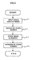
- Fig. 6 is a flow chart showing the flow of processing according to the image processing method of the first embodiment of the present invention.
- step S1 When a raster image is input into an image processing apparatus (step S1), the bit-plane number of the input raster image is reduced (step S2).
- the raster image whose bit-plane number has been reduced is stored in a memory or the like (step S3). After that, the raster image stored in the memory is read out, and the bit-plane number of the raster image is increased (step S4).
- the processing for reducing and increasing the bit-plane number with less logic elements. More specifically, it is desirable that the image processing should involve a sufficiently small number of logic elements as compared to the number of logic elements (the number of transistors, cells, etc.) of the memory, which can be reduced by the processing. Generally, the processing for reducing and increasing the bit-plane number requires the small number of logic elements, and therefore, the bit-plane number can be suitably reduced/ increased.
- bit dropping that is, "truncation of specific bits”. In this case, calculation or computing is not necessary.
- the bit-number reduction/ addition is carried out at a constant data compression rate ((amount of data before compression amount of data after compression)/ amount of data before compression). Consequently, it is possible to facilitate various types of image processing in an image processing apparatus (a display system), which compresses data of an original image to store the image data in a memory, and decompresses the stored image data to display the image.
- a display system which compresses data of an original image to store the image data in a memory, and decompresses the stored image data to display the image.
- the data of a raster image may be transmitted via a transmission bus having a prescribed bus width instead of storing the data of the raster image in the memory.
- a transmission bus between an operation section or part for reducing the bit-plane number and an operation section for increasing the bit-plane number does not have a width sufficient to transmit a raster image in its original form.
- the bit-plane number of the raster image is reduced to the number within the capacity of the transmission bus, and the raster image whose bit-plane number has been reduced is transmitted.
- the bit-plane number of the raster image is increased by bit addition processing, and then the image is output to an image display section or the like.
- the raster image can be displayed on the image display section.
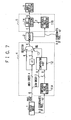
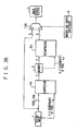
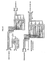
- Fig. 7 is a block diagram schematically showing the configuration of an image processing apparatus according to the second embodiment of the present invention.
- an RGB raster image 1 with 6 bits per color component output from a computer is processed in an image processing former stage 4.
- a raster image with 4 bits per color component is stored in a memory 2.
- the stored raster image with 4 bits per color component is converted into an image with 6 bits per color component in an image processing latter stage 5, and the image is output to an image display section 3 capable of 6-bit display.
- Fig. 7 shows a block configuration for one color of R, G and B, and the image processing apparatus has the same configurations for the other two colors in parallel.
- the image processing former stage 4 comprises a threshold value generator 11A, a comparator 12, a selector 13 and a subtracter. Low order 2 bits of 6-bit gray level data of the input raster image 1 are sent to the comparator 12, and compared with a 2-bit signal output from the threshold value generator 11A in the comparator 12.
- Fig. 8 is a chart illustrating a method for generating output signals from the threshold value generator.
- a dither matrix based on ordered dithering is utilized as threshold values.
- the threshold value generator 11A generates an output signal based on X-Y coordinate values (x, y) of an input pixel.
- [x mod 2] indicates the remainder when an X coordinate value (x) of the pixel is divided by 2
- [y mod 2] indicates the remainder when a Y coordinate value (y) of the pixel is divided by 2.
- An output value is obtained according to these [x mod 2] and [y mod 2].
- the comparator 12 When A ⁇ B, where the value of the low order 2 bits of 6-bit gray level data of the input raster image 1 is A, and the output value of the threshold value generator 11A is B, the comparator 12 outputs "1", and otherwise, the comparator 12 outputs "0" as a SEL signal to the selector 13.
- the SEL signal is a select signal of the selector 13.
- the value of high order 4 bits of 6-bit gray level data of the input raster image 1 and a value obtained by subtracting 1 therefrom by the subtracter are input into the selector 13.
- the selector 13 directory outputs the value of the high order 4 bits when the SEL signal output from the comparator 12 is "0" , while the selector 13 outputs the value obtained from the subtracter when the SEL signal is "1".
- a 4-bit output signal of the image processing former stage 4 is obtained.
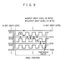
- Fig. 9 is a diagram showing a frame format of processing in the image processing former stage.
- Fig. 9 input 6-bit gray level data indicated on the left side by the vertical axis are converted into output 4-bit gray level data indicated on the left side with respect to each pixel (pixel position) indicated by the horizontal axes.
- “ ⁇ ” in the leftmost pixel position indicates that an input gray level is "011110". Since the value is in between threshold values "011111” and “011011", it is rounded up or down to a value indicated by a horizontal line between them.
- " ⁇ ” indicates output gray level, and in this case, output gray level is "0110” .
- the above-described processing is performed with respect to each pixel position, to thereby convert the 6-bit gray level data of the raster image 1 into 4-bit output gray level.
- the input value is converted into a 4-bit value that is larger than and closest to the threshold value.
- one of 4-bit gray level values over the threshold value in the drawing, which is closest to the threshold value is selected as an output gray level value.
- 6-bit gray level data is converted into 4-bit gray level data based on thresholds which vary according to the X-Y coordinate values (x, y) of an input pixel.
- the bit-plane number of a raster image is reduced, and the raster image is stored in the memory 2.
- the raster image with less bit-plane number stored in the memory 2 is converted into an image with 6 bits per color component in the image processing latter stage 5, and sent to the image display section 3.
- the image processing latter stage 5 comprises a bit addition section 14 and a threshold value generator 11B.
- the threshold value generator 11B is of the same construction as the threshold value generator 11A.
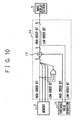
- Fig. 10 is a circuit diagram showing the internal configuration of the bit addition section.
- the bit addition section 14 attaches a value obtained by applying OR logic to a 4-bit signal output from the memory 2 as a low order bit to the 4-bit signal to produces a 5-bit signal. After that, the bit addition section 14 adds a high order bit of 2 bits output from the threshold value generator 11B by an adder 17. In addition, the bit addition section 14 attaches a low order bit output from the threshold value generator 11B to the 5-bit signal as high order bits obtained from the adder 17 to produce a 6-bit signal. Thus, the 6-bit signal is sent to the image display section.
- a value obtained by applying OR logic to the 4-bit signal is attached as a low order bit to the 4-bit signal in order to minimize the difference between an input signal and an output signal.
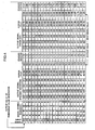
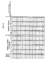
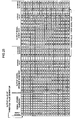
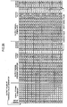
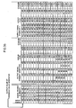
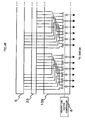
- Figs. 3 to 5 are lists showing input signals, signals (4-bit value) stored in the memory 2 based on the output value of the threshold value generator, and output signals (6-bit value).
- respective input signals and the signal values of the threshold value generator are expressed in decimal numbers.
- Each signal stored in the memory indicates a 4-bit gray level value expressed in a decimal number
- each output signal indicates a 6-bit gray level value expressed in a decimal number.
- Figs. 3 to 5 also shows output signals, average output signal values corresponding to respective input signals, differences between the respective average values and input signal values, and standard deviations in the output signals by multi-valued dithering (prior art).
- the difference between the average value and the input signal value is -1.5. Consequently, more variations are shown in colors and brightness as compared to the case of applying OR. Nevertheless, the difference between the two values is made smaller with regard to input signals 2 to 40 as compared to the prior art.
- the same signals are stored in the memory for respective input signals 0 to 3, and, therefore, the same signals are output. If it is required to produce distinct shades on a gray scale corresponding to the respective input signals, the gray level conversion of the input signals is usable.
- the highest gray level and the lowest gray level with respect to each of all dither values after the above-described processing should be the same as before.
- This can be realized by setting the condition where, for example, when a signal value stored in the memory is 0, the dither value is not to be added to the output value in addition to the aforementioned gray level conversion of the input signal. It is obvious that any other processing method can be employed so long as the aforementioned conditions are satisfied.
- the image processing former stage 4 has been described as including the comparator 12 and the selector 13, it may be implemented by a subtracter and a quantizer 18 as shown in Fig. 11 to obtain the same output.
- the quantizer 18 has a function for directly outputting high order 4 bits of 6 bits of an input.
- ordered dithering is utilized in the threshold value generator by way of example and without limitation. More specifically, the above-mentioned effects can be achieved with the use of a two-dimensional dither matrix, by which the same pattern is repeated for a micro-length as one cycle in both vertical and horizontal directions of an image. As the cycle of the dither matrices becomes smaller, the frequency of cyclic noise gets higher, and the noise is made virtually imperceptible. For this reason, it is most desirable to use a two-dimensional dither matrix of 2-pixel cycle for both vertical and horizontal directions.
- the threshold value generator 11B is of the same construction as the threshold value generator 11A. Therefore, there may be provided only one threshold value generator, which switches from the threshold value generator 11A to 11B and vice versa as shown in Fig. 12 . In this case, control is required for determining whether the output of the threshold value generator 11 is input to the comparator 12 or to the bit addition section 14. An example of the control method is illustrated in Fig. 12 .
- an input/ output switch controller 16 outputs a control signal SEL 2 to a selector 13A and a demultiplexer 15.
- the input/- output switch controller 16 selects and outputs "0" as the SEL 2 when sending the output of the threshold value generator 11 to the comparator 12, and selects and outputs "1" when sending the output to the bit addition section 14.
- the image processing apparatus of the second embodiment comprises the image processing former stage 4 for performing image processing to reduce the bit-plane number of the raster 1, the memory 2 for storing output signals (raster image) of the image processing former stage 4, and the image processing latter stage 5 for restoring the bit-plane number of the raster image sent from the memory 2 to the original number, and image processing is performed in reverse ways in the respective image processing former stage 4 and the image processing latter stage 5.
- image processing is performed in reverse ways in the respective image processing former stage 4 and the image processing latter stage 5.
- image processing can be performed by software.
- Fig. 13 is a flow chart illustrating an example of an image processing method in the image processing former stage
- Fig. 14 is a flow chart illustrating an example of an image processing method in the image processing latter stage according to this embodiment.
- operations in both the image processing former stage and the image processing latter stage are executed through software, it does not matter if only one of them is implemented by software and the other is implemented by hardware.
- Fig. 13 shows an image processing method on the occasion when an input signal is composed of 6 bits, and the bit-plane number of the signal after compression is b bits (b: an integer 2 to 6).
- the X coordinate of a pixel: x, and the Y coordinate of the pixel: y are input in the image processing former stage 4 (step S11).
- a dither matrix necessary to generate threshold values is defined (step S12).
- a matrix called Bayer ordered dither matrix [[0, 8, 2, 10], [12, 4, 14, 6], [3, 11, 1, 9], [15, 7, 13, 5]]
- a threshold value is generated based on the pixel coordinate values x and y (step S13).
- the method of generating the threshold value is as shown in the drawing.
- [x mod 4] indicates the remainder when an X coordinate value x is divided by 4.
- a threshold value d is subtracted from input gray level signal, and low order bits are truncated at step S14.
- high order 4 bits are output.
- an gray level signal: I of b bits, the X coordinate of a pixel: x, and the Y coordinate of the pixel: y are input in the image processing latter stage 5 (step S21).
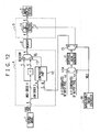
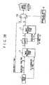
- Fig. 15 is a block diagram showing the first example of the configuration of an image processing apparatus according to the third embodiment of the present invention.
- the image processing apparatus according to the third embodiment differs from that of the second embodiment in the presence of a selector 13B for determining whether to send the raster image 1 directly to the image display section 3 or to send the raster image 1 from the memory 2 to the display section 3 and a memory use switch controller 6 for conducting the selection control in the selector 13B between the image processing former stage 4 and the image processing latter stage 5.
- the memory use switch controller 6 controls the selector 13B according to images to be sent to the image display section 3. For example, when a still image is being displayed, the image remains unchanged. Therefore, the memory use switch controller 6 outputs "1" so as to display an image stored in the memory 2. Accordingly, the selector 13B sends a raster image output from the image processing latter stage 5 to the image display section 3. On the other hand, when a moving image is being displayed, the memory use switch controller 6 outputs "0" to the selector 13B so as to directly display the raster image 1 on the image display section 3 without storing it in the memory.
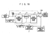
- Fig. 16 is a block diagram showing the second example of the configuration of the image processing apparatus according to the third embodiment of the present invention.
- the memory use switch controller 6 outputs "0" , that is, when the raster image 1 is directly displayed on the image display section 3 without the intervention of the memory 2, processing in the image processing former stage 4, the memory 2 and the image processing latter stage 5 is stopped with the use of a processing ON/ OFF controller 7.
- the memory 2 and the image processing latter stage 5 it is possible to reduce electric power consumption.
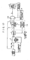
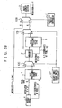
- Fig. 17 is a block diagram schematically showing the configuration of an image processing apparatus according to the fourth embodiment of the present invention.
- the image processing apparatus according to the fourth embodiment differs from that of the third embodiment shown in Fig. 15 in the configuration of a bit addition section 14A, and in that the output of the memory use switch controller 6 is input into a gray level controller 7 which provides gray level control in the image display section 3.
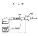
- Fig. 18 is a block diagram schematically showing the configuration of the bit addition section according to the fourth embodiment of the present invention.
- the bit addition section 14A combines the output of the memory 2 with the output of the threshold value generator 11B as high order 4 bits and low order 2 bits, respectively, to output them to the selector 13B.
- the configuration of the bit addition section 14A is considerably simplified as compared with that of the bit addition section 14 according to the second embodiment of the present invention shown in Fig. 10
- Figs. 19 to 21 are lists showing input signals, signals stored in the memory and output signals from the image processing latter stage in the fourth embodiment of the present invention.
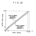
- the average of the output signal values is smaller than the input signal value when the configuration of Fig. 10 is changed into that of Fig. 18 .
- the gray level controller 7 adjusts an output gray level signal as shown in Fig. 22 so that it becomes higher in gray level than the output signal shown in Figs. 19 to 21 .
- Examples of the gray level controller 7 include one in which a look-up table is constructed to carry out the conversion of input signals. Besides, if the gray level controller 7 is realized in hardware, the reference voltage of liquid crystal may be changed so that the V-T characteristics of liquid crystal vary according to the values output from the memory use switch controller 6 when an LCD (liquid crystal display) which uses analog supply to display an image or an organic EL (electroluminescent) display is employed as the image display section.
- Fig. 23 is a block diagram schematically showing the configuration of an image processing apparatus according to the fifth embodiment of the present invention.
- the image processing apparatus according to the fifth embodiment differs from that of the third embodiment shown in Fig. 15 in that the bit-plane numbers for color components R, G and B, which are stored in the memory 2, are 4, 5 and 3, respectively.
- the memory has the same capacity as that of the third embodiment of the present invention.
- the large bit-plane number is allocated for G, while the small bit-plane number is allocated for B.
- G has the greatest effect on brightness components, while B has the least effect.
- B has the least effect.
- a grainy feeling can be more suppressed.
- the bit-plane number is set as above described, color differences in B are increased, thereby deteriorating the quality of flesh-colored part of an image.
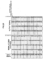
- Figs. 24 to 26 are lists showing input signals, signals stored in the memory and output signals from the image processing latter stage for the color component B in the fifth embodiment of the present invention.
- the drawings also shows output signals, average output signal values corresponding to respective input signals, differences between the respective average values and input signal values, and standard deviations in the output signals by multi-valued dithering (prior art).
- the standard deviation of this embodiment is reduced in almost all gray levels, and is a stably low value. From this it is to be understood that, according to this embodiment, color differences and a grainy feeling can be suppressed even when the bit-plane number for each color component is changed.
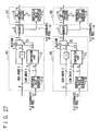
- Fig. 27 shows the configurations of image processing former stages 4G and 4B, and image processing latter stages 5G and 5B.
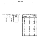
- threshold value generators 11G and 11B generate output signals by a generation method illustrated in Fig. 28 .
- Fig. 29 shows an example of this configuration.
- the threshold value generator 11 shown in Fig. 29 employs the generation method for the threshold value generator 11B shown in Fig. 28 , and utilizes high order 2 bits as the output for the R component and only one high order bit as an output for the G component. This eliminates the need for the setting of the threshold value generator 11 with respect to each of the color components R, G and B, thus increasing the efficiency.
- an image processing apparatus which enables 6-bit worth of display on an image display section that displays an image with 4 bits per color component making use of FRC (Frame Rate Control), will be described.
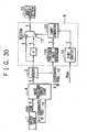
- Fig. 30 is a block diagram schematically showing the configuration of an image processing apparatus according to the sixth embodiment of the present invention.
- the image processing apparatus according to the sixth embodiment differs from that of the second embodiment shown in Fig. 7 in the presence of an FRC image processing latter stage 9 instead of the image processing latter stage 5 in Fig. 7 , and in that VSync indicating the start of a frame is input into the FRC image processing latter stage 9, and an image display section 3A can display an image with 4 bits per color component.
- VSync indicating the start of a frame is input into the FRC image processing latter stage 9
- an image display section 3A can display an image with 4 bits per color component.
- only one block of those of R, G and B is seen in the drawing for simplicity.
- the FRC image processing latter stage 9 comprises the threshold value generator 11B for generating a threshold value based on X-Y coordinates of a pixel, a 2-bit counter 19 for counting VSync, a carry generator 20 for generating a carry based on the output of the threshold value generator 11B and the 2-bit counter 19, and the selector 13 for determining whether to output a value obtained by adding 1 to the output of the memory 2 or to directory output the output value to the image display section 3 according to the carry value.
- the threshold value generator 11B generates the output as shown in Fig. 8 .
- the output values are the same as those in the second embodiment of the present invention.
- the 2-bit counter 19 counts VSync each time VSync is input, and output values therefrom change as 00 ⁇ 11 ⁇ 01 ⁇ 10 ⁇ 00 ⁇ .
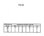
- Fig. 31 is a state transition diagram showing the transitions. As can be seen in Fig. 31 , output values are made as hereinafter described.
- the carry generator 20 sets a carry value based on a threshold value, which is the output of the threshold value generator 11B, and the output value of the 2-bit counter 19.
- Fig. 32 shows relations among the threshold values, the counter output values and the carry output values.
- the carry generator 20 outputs "1" when the threshold value > the counter output value. Otherwise, the carry generator 20 outputs "0". In this manner, by defining 4 frames as 1 cycle, the carry generator 20 generates a carry corresponding to the threshold in the cycle.
- the selector 13 selects a signal to be output based on the carry value.
- the selector 13 outputs an output value from the memory 2 to the image display section 3 when the carry value is "0".
- the selector 13 outputs a value obtained by adding 1 to the output value from the memory 2 when the carry value is "1".
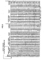
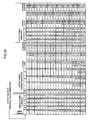
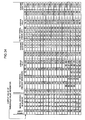
- Figs. 33 to 35 are lists showing input signals, signals stored in the memory and output signals from the FRC image processing latter stage 9 in the sixth embodiment of the present invention.
- the drawings also shows output signals, average output signal values corresponding to respective input signals, differences between the respective average values and input signal values, and standard deviations in the output signals by multi-valued dithering (prior art).
- the respective output signals are of 4 actually bits, values obtained through 4 to 6 bits conversion are utilized so that the differences between the input and output signals can be compared with each other.
- the output signal from the FRC image processing latter stage 9 is an average value for 4 frames (1 cycle) obtained by the FRC image processing latter stage 9.
- the standard deviation of this embodiment is reduced in almost all gray levels, and is a stably low value.
- the standard deviation also bears comparison with that of Figs. 3 to 5 . From this it is to be understood that, according to the present invention, an image equivalent in quality to a 6-bit image can be obtained with a 4-bit memory and a 4-bit display.
- Fig. 36 is a block diagram showing an example of the configuration of an image processing apparatus according to the seventh embodiment of the present invention.
- the image processing apparatus according to the seventh embodiment differs from that of the third embodiment in the presence of a compressor 4A and a decompressor 5A instead of the image processing former stage 4 and the image processing latter stage 5.
- the memory use switch controller 6 controls the selector 13B according to an image to be sent to the image display section 3. For example, when a still image is being displayed, the image remains unchanged. Therefore, the memory use switch controller 6 outputs "1" so as to display an image stored in the memory 2. Accordingly, the selector 13B sends a raster image output from the decompressor 5A to the image display section 3. On the other hand, when a moving image is being displayed, the memory use switch controller 6 outputs "0" to the selector 13B so as to directly display the raster image 1 on the image display section 3 without storing it in the memory 2.
- the compressor 4A and the decompressor 5A need not perform compression/ decompression processing having a special relationship (for example, the same two-dimensional dither matrix should be used) for image signals input into the memory 2 and image signals read out therefrom.
- the compressor 4A and the decompressor 5A may use different two-dimensional dither matrices to perform compression/ decompression processing for image signals input into the memory 2 and image signals read out of the memory 2, respectively.
- compressor 4A and the decompressor 5A may perform other compression/ decompression processing without using a two-dimensional dither matrix to achieve the same effects as above described.
- Fig. 37 is a block diagram showing an example of the configuration of an image processing apparatus according to the eighth embodiment of the present invention.
- the image processing apparatus according to the eighth embodiment further comprises the processing ON/ OFF controller 7 in addition to the configuration of the image processing apparatus in the seventh embodiment.
- the processing ON/ OFF controller 7 stops processing in the compressor 4A, the memory 2 and the decompressor 5A when the memory use switch controller 6 outputs "0" , that is, when the raster image 1 is directly displayed on the image display section 3 without the intervention of the memory 2.
- the processing ON/ OFF controller 7 stops processing in the compressor 4A, the memory 2 and the decompressor 5A when the memory use switch controller 6 outputs "0", that is, when the memory 2 is not to be used.
- Fig. 38 is a block diagram showing an example of the configuration of an image processing apparatus according to the ninth embodiment of the present invention.
- the image processing apparatus according to the ninth embodiment differs from that of the third embodiment in that the memory 2 has a capacity equivalent to that of the image display section 3 which is capable of displaying an image with 6 bits per color component with a resolution of X*Y pixels (namely, the memory 2 can store an image of X*Y pixels).
- the resolution of a display unit means the maximum number of pixels which the display unit (e.g. the image display section 3) can represent horizontally and vertically on the screen at once.
- the resolution of a display unit is 640 by 480 (pixels)
- it is provided with 640 pixels in a horizontal direction and 480 pixels in a vertical direction.
- the display unit has the ability to display an image formed of less than 640 by 480 pixels on the screen at once.
- the resolution of an image means the total number of pixels that form an image, and is represented as the product of the number of pixels in a vertical direction and that in a horizontal direction. For example, if the resolution of an image is 640 by 480 (pixels), the image occupies an area in the shape of a rectangle represented by 640 pixels in a horizontal direction and 480 pixels in a vertical direction.
- the image display section 3 can display the arbitrary area of the image whose resolution is higher or greater than that of the display section 3.
- the image stored in the memory 2 is a high-resolution image such as a scrolling image (namely, an image composed of pixels more than the resolution of the image display section 3)
- the image can be displayed without receiving the image from the outside in every frame cycle.
- the highest resolution of an input image is X * Y. More specifically, when an image input as the raster image 1 is smaller than the area of X * Y pixels, the memory use switch controller 6 outputs "0" to the selector 13B so as to directly display the raster image 1 on the image display section 3 without the intervention of the memory 2.
- the respective images can be stored in the memory 2 by compressing them in the image processing former stage 4 in the same manner as described hereinbefore.
- the respective raster images can be displayed on the image display section 3 after reading them out of the memory 2 and expanding them in the image processing latter stage 5.
- the image stored in the memory 2 is a high-resolution image such as a scrolling image (namely, an image composed of pixels more than the resolution of the image display section 3), the image can be displayed without receiving the image from the outside in every frame cycle.
- a high-resolution image such as a scrolling image (namely, an image composed of pixels more than the resolution of the image display section 3)
- Fig. 39 is a block diagram showing an example of the configuration of an image processing apparatus according to the tenth embodiment of the present invention.
- the image processing apparatus according to the tenth embodiment further comprises a selector 13C in between the image processing former stage 4 and the memory 2, a selector 13D in between the image processing latter stage 5 and the selector 13B, and a memory input signal switch controller 27 for controlling the selectors 13C and 13D differently to that of the ninth embodiment.
- the memory input signal switch controller 27 selects or determines whether an image to be stored in the memory 2 is a compressed image or an uncompressed image with reference to the resolution of the input image and the like. In the following description, while a compressed image or an uncompressed image is selected referring to resolution, the selection between them may be carried out with reference to the volume of data of an image such as the bit-plane number.
- the memory input signal switch controller 27 outputs "0" to the selectors 13C and 13D, while the memory use switch controller 6 outputs "1" to the selector 13B. Consequently, an uncompressed image is stored in the memory 2, and displayed on the image display section 3.
- the memory input signal switch controller 27 outputs "1" to the selectors 13C and 13D, and the memory use switch controller 6 outputs "1" to the selector 13B. Accordingly, an image compressed in the image processing former stage 4 is stored in the memory 2. After that, the image is read out of the memory 2 to be expanded in the image processing latter stage 5, and the expanded image is displayed on the image display section 3.
- the memory use switch controller 6 outputs "0" to the selector 13B so as to directly display the raster image 1 on the image display section 3 without the intervention of the memory 2 as in the ninth embodiment.
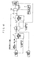
- Fig. 40 is a block diagram showing an example of the configuration of an image processing apparatus according to the eleventh embodiment of the present invention.
- the raster image 1 which is an original image, is divided into an image 1A and text information 1B, and then input to the image processing apparatus.
- the image processing apparatus differs from that of the ninth embodiment in the presence of an image compositor 28.
- the image compositor 28 generates a composite image of the image 1A whose bit-plane number has been increased in the image processing latter stage 5 and the text information 1B.
- the memory use switch controller 6 outputs "1" to the selector 13B to input the image 1A into the image processing former stage 4.
- the image 1A whose bit-plane number has been reduced to "5"
- the image processing latter stage 5 is expanded in the image processing latter stage 5 in the same manner as described above so that the bit-plane number is increased from "5" to "6".
- the image compositor 28 generates a composite image of the image 1A whose bit-plane number has been increased in the image processing latter stage 5 and the text information 1B read out of the memory 2.
- the composite image is displayed on the image display section 3.
- a raster image is divided into two layers, and input in the image processing apparatus.
- the raster image cannot be stored in the memory 2 unless it is compressed, at least data of one of the layers is compressed or the bit-plane number is reduced to store the image in the memory 2. After expanding the compressed data or increasing the reduced bit-plane number, the two layers are combined. Thus, a composite image can be displayed.
- an overlay display of text can be implemented by the image compositor 28.
- the image compositor 28 there is no need for the setting of a new memory to display overlay images.
- the image processing apparatus of this embodiment can changes the image 1A and the text information 1B independently.
- the image 1A is a still image and the text information 1B is a clock for indicating the time
- only the text information 1B may be obtained at a regular interval (e.g. every second or every minute), and stored in the memory 2 to dispense with processing in the image processing former stage 4, the memory 2 and the image processing latter stage 5.
- a regular interval e.g. every second or every minute
- a multiple tone image and text information are cited as the two layers that form a raster image by way of example and without limitation.
- superimpose display of two images may be applicable.
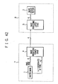
- Fig. 41 is a block diagram showing an example of the configuration of an image processing apparatus according to the twelfth embodiment of the present invention.
- a signal for displaying the raster image 1 is divided into two layers, the image 1A and a control signal 29 for each pixel, and input into the image processing apparatus.
- the image processing apparatus differs from that of the ninth embodiment in that when the image 1A and the control signal 29 cannot be stored in the memory 2 without compression, the image 1A is compressed or the bit-plane number thereof is reduced to store them in the memory 2, and an image obtained by expanding the compressed image or increasing the reduced bit-plane number is displayed on the image display section 3 based on the control signal 29.
- the memory use switch controller 6 outputs "1" to the selector 13B to input the signal for displaying the raster image 1 into the image processing former stage 4.
- the image 1A whose bit-plane number has been reduced to "5" , is read out of the memory 2, and expanded in the image processing latter stage 5 in the same manner as described above so that the bit-plane number is increased from "5" to "6".
- the image 1A whose bit-plane number has been increased is displayed on the image display section 3 based on the control signal 29 for each pixel read out of the memory 2.
- a signal for displaying the raster image 1 is divided into at least one image and at least one control signal, and input in the image processing apparatus.
- at least one image is compressed or the bit-plane number thereof is reduced to store the signal in the memory 2.
- An image obtained by expanding the compressed image or increasing the reduced bit-plane number can be displayed based on the control signal.
- the image processing apparatus of this embodiment can changes the image 1A and the control signal 29 independently as in the eleventh embodiment.
- the control signal 29 may be updated to dispense with processing in the image processing former stage 4, the memory 2 and the image processing latter stage 5.
- a raster image is transmitted from a first unit to a second unit, where transmission capacity can be reduced. In the following, this construction will be described.
- Fig. 42 is a block diagram schematically showing the configuration of an image transmission apparatus according to the thirteenth embodiment of the present invention.
- the image transmission apparatus according to the thirteenth embodiment of the present invention comprises a first unit 7 for sending a raster image and a second unit 8 for receiving the raster image.
- the raster image 1 with 6 bits per color component is converted into an image with 4 bits per color component at the image processing former stage 4, and sent to the second unit 8.
- the raster image received from the first unit 7 is restored to the image with 6 bits per color component at the image processing latter stage 5, and output to the image display section 3.
- the image processing former stage 4 and the image processing latter stage 5 have the same construction as described previously for those in the above embodiments.
- a raster image can be transmitted from the first unit to the second unit without any appreciable decrease in image quality, and image transmission can be performed with less transmission capacity.
- This form is advantageous where transmission capacity is insufficient for an image or the number of transmission buses between the first unit and second unit is to be reduced.
- the second unit 8 provided to the image transmission apparatus of this embodiment also represents an image reception apparatus according to a preferred embodiment of the present invention.
- the image reception apparatus of the present invention receives a raster image whose bit-plane number has been reduced as compared to an original image, and increases the bit-plane number of the received image as with the second unit 8. Thus, it is possible to produce an image that is comparable in quality to the original image. In addition, since the bit-plane number of an image is reduced to the number less than that of an original image at the transmitting end, the image reception apparatus can receive the image efficiently.
- the bit-plane number of the raster image is reduced at the transmitting end so that the apparatus can receive the raster image with less bit-plane number, and thereafter, the apparatus increases the bit-plane number of the image. Thereby, the apparatus can receive the respective color components of the image comparable in quality to the original image in parallel.
- Fig. 43 shows an image transmission apparatus according to the fourteenth embodiment of the present invention.
- the image transmission apparatus comprises a first unit 7 for sending a raster image and second units 8a, 8b and 8c for receiving the raster image.
- transmission buses between the first unit 7 and the second units 8a, 8b and 8c have bus widths of 15 bits, 12 bits and 9 bits, respectively.
- the first unit 7 includes the image processing former stage 4, a bit-plane number reduction controller 50, a selector 51 and a demultiplexer 52.
- the bit-plane number of the raster image 1 (6 bits per color component) is reduced to a prescribed number in the image processing former stage 4, and a raster image with the bit-plane number corresponding to an instruction from the bit-plane number reduction controller 50 is output to the selector 51.
- the bit-plane number reduction controller 50 controls the selector 51 depending on which of the second units 8a to 8c the raster image 1 is to be transmitted to, and instructs the image processing former stage 4 to output an image with the bit-plane number suitable for the receiving end.
- the bit-plane number reduction controller 50 controls the demultiplexer 52 to select one of the transmission buses for the raster image whose bit-plane number has been reduced in the image processing former stage 4.
- the second unit 8a includes an image processing latter stage 5a and an image display section 3a.
- the image processing latter stage 5a the raster image with 5 bits per color component transmitted from the first unit 7 is processed in the same manner as previously set forth to restore it to the raster image with 6 bits per color component.
- the image display section 3a displays the restored raster image with 6 bits per color component.
- the second unit 8b restores the raster image with 4 bits per color component to the image with 6 bits per color component in the image processing latter stage 5b, while the second unit 8c restores the raster image with 3 bits per color component to the image with 6 bits per color component in the image processing latter stage 5c. Otherwise the second units 8b and 8c operate in the same manner as the second unit 8a.
- a case where the raster image 1 is transmitted to the second unit 8a will be described.
- the bit-plane number reduction controller 50 controls the selector 51 to input a raster image suitable for the receiving unit, that is, to input the raster image with 5 bits per color component into the demultiplexer 52.
- the bit-plane number reduction controller 50 sends a control signal "a" to the selector 51. Since the control signal output from the bit-plane number reduction controller 50 is "a" , the raster image input into the demultiplexer 52 is output to the transmission bus leading to the second unit 8a.
- the second unit 8a processes the raster image received from the first unit 7 in the image processing latter stage 5a to restore it to the raster image with 6 bits per color component, and displays the restored image on the display section 3a.
- the image transmission apparatus can determine the number of bit-planes reduced from a raster image depending on a receiving unit. Consequently, it is possible to transmit a raster image with the bit-plane number corresponding to the bus width of a transmission bus to the receiving unit and the capacity of the image processing latter stages 5a to 5c. Thus, the efficiency of transmission capacity is improved.
- the present invention is aimed at reducing chip size and electric power consumption, the image processing section is not required to perform any complicated processing, and has a simple construction. Therefore, the present invention can achieve the above-described effects when applied to the driver and controller chip of a display unit having a built-in memory. Further, the present invention is applicable to a polysilicon circuit in which such driver and controller is set on a glass substrate.
- Fig. 44 shows a liquid crystal display (LCD) in which an image processing section and a drive circuit section are formed on a glass substrate with the use of a polysilicon thin film transistor circuit.
- An input signal is composed of 6 bits per color component, R, G and B, the memory has a capacity of 4 bits per color component; R, G and B, and an output is of 6 bits per color component, R, G and B.
- the raster image 1 from the outside is displayed on a liquid crystal display section 10.
- the liquid crystal display section 10 includes a matrix of pixels 31, thin film transistors 32, a plurality data lines 33 and a plurality of gate lines 34, which are arranged so as to form a lattice with respect to each pair of the pixel 31 and the thin film transistor 32, each connecting to the thin film transistor 32.
- a signal of the data line 33 connected to the thin film transistor 32 is written to each pixel 31 when the thin film transistor 32 has entered into the ON state according to a signal from the gate line 34.
- the raster image 1 is sent to the image processing former stage 4 and data registers 22.
- the raster image input to the image processing former stage 4 undergoes image processing as previously described for the first to twelfth embodiments, and stored in the memory 2 having a capacity of 12 bits in total for the color components R, G and B. Thereafter, data is read out of the memory 2 if necessary, and image processing is performed in the image processing latter stage 5.
- the output of the image processing latter stage 5 is sent to the selector 13B.
- image processing of the image processing former stage 4, the memory 2 and the image processing latter stage 5 is performed in the same manner as previously described for the first to twelfth embodiments.
- the X-Y coordinates of a pixel are required when data is written to or read out of the memory 2.
- the control signal is not limited to the X-Y coordinates of a pixel.
- a control signal from which the X-Y coordinates of a pixel can be derived, such as VSync, Hsync and CLK may be used.
- a memory controller 26 makes a switch between reading and writing, and controls the addresses of data input/ output for the memory 2. At least the X-Y coordinates of a pixel are input in the memory controller 26 as with the image processing former stage 4 and the image processing latter stage 5.
- Fig. 45 is a circuit diagram showing sift registers 21A and the data registers 22 of the LCD. Concerning a raster image input to the data registers 22, 6-bit data is sequentially stored on the basis of an output signal from the respective sift registers (S/R) 21A, and latched by latches 23. The outputs of the latches 23 are sent to the selector 13B.
- Fig. 46 is a circuit diagram showing the configuration of the selector 13B of the LCD.
- the selector 13B selects data to be sent to the a DAC 24 depending on whether an image stored in the memory 2 having passed through the image processing latter stage 5 is displayed or an image from the outside is directly displayed based on control data from the memory use switch controller 6.
- the DAC 24 converts the digital signal with 6 bits per color component from the selector 13B into an analog signal, and outputs the signal to a desired data line through a data line selector 25.
- the output of the data line selector 25 is sent to the liquid crystal display section 10, and written to the pixel 31 through the thin film transistor 32 corresponding to the gate line 34 selected by the sift register 21B.
- the fifteenth embodiment of the present invention it is possible to obtain an LCD having a built-in image processing circuit as previously described for the first to twelfth embodiments on a glass substrate.
- the respective image processing former stage 4 and the image processing latter stage 5 can be formed of fewer transistors.
- Fig. 47 shows an example of the logical configurations of the image processing former stage 4 and the image processing latter stage 5 for storing a 6-bit signal in a 4-bit memory and expanding the signal to a 6-bit signal.
- the image processing former stage 4 and the image processing latter stage 5 include only 2-input/ 3-input NAND circuits and inverters. From this it is to be understood that the size of the image processing circuit is sufficiently smaller than the memory area, and the size of the circuit section can be reduced.
- multi-valued dither processing with the use of a two-dimensional dither matrix and bit addition processing based on the two-dimensional dither matrix are performed as a way of image processing.
- the present invention is not to be restricted by those embodiments but it will suffice so long as aforementioned pseudo outlines, pseudo colors and a grainy feeling can be suppressed.
- multi-valued dither processing is performed with the use of a two-dimensional dither matrix when reducing the bit-plane number of a raster image, and bit addition processing is performed based on the two-dimensional dither matrix used for the multi-valued dither processing when increasing the bit-plane number.
- bit addition processing is performed based on the two-dimensional dither matrix used for the multi-valued dither processing when increasing the bit-plane number.
- other image processing methods by which image processing is performed in reverse ways when increasing and reducing the bit-plane number may be applicable, as for example by using a random dither instead of a two-dimensional dither matrix to perform multi-valued dither processing.
- Image processing may be performed through software in the image processing apparatus and the image transmission apparatus according to the other embodiments as in the second embodiment.
- a bit-mapped image to be sent to a display unit can be compressed/ decompressed with fewer logic elements, thereby enabling reductions in memory capacity and transmission capacity.
- the difference between an image which has undergone bit addition processing and an original image is small as compared to multi-valued dithering.
- a compressed image is selected when a still image is being displayed, while when a moving picture is being displayed, the image is directly displayed without image processing. Since an image can be displayed without the intervention of a storage (e.g. memory) when displaying a moving picture, electric power consumption can be reduced by stopping the operation of the storage.
- a storage e.g. memory
- the image in the case of displaying an image which exceeds the maximum resolution of a display unit, such as a map, the image can be stored with insufficient memory capacity by compression/ decompression of the bit-plane number. Thereby, it is possible to scroll through the image on the display without reacquisition of the image from outside, which reduces electric power consumption associated with image display.
- an image transmission apparatus and an image processing method for improving the efficiency of transmission capacity For example, in the case of transmitting an RGB raster image with 6 bits per color component (18 bits in total) via a transmission bus which is only 16 bits wide, the raster image is compressed by reducing the bit-plane number. Thus, data can be transmitted in parallel.
- the image processing apparatus in a display unit in which a drive circuit is formed on a substrate (e.g. glass substrate), the image processing apparatus can be formed on the substrate by the same process. Therefore, by the application of the present invention to a display unit, the size of the display unit can be reduced due to less memory, and also electric power consumption can be reduced.
- a substrate e.g. glass substrate
Landscapes
- Engineering & Computer Science (AREA)
- Multimedia (AREA)
- Signal Processing (AREA)
- General Physics & Mathematics (AREA)
- Theoretical Computer Science (AREA)
- Physics & Mathematics (AREA)
- Computer Hardware Design (AREA)
- Crystallography & Structural Chemistry (AREA)
- Chemical & Material Sciences (AREA)
- Controls And Circuits For Display Device (AREA)
- Compression Of Band Width Or Redundancy In Fax (AREA)
- Image Processing (AREA)
- Compression Or Coding Systems Of Tv Signals (AREA)
- Control Of Indicators Other Than Cathode Ray Tubes (AREA)
- Storing Facsimile Image Data (AREA)
- Liquid Crystal Display Device Control (AREA)
Priority Applications (2)
| Application Number | Priority Date | Filing Date | Title |
|---|---|---|---|
| EP20090165642 EP2112649A3 (en) | 2001-09-14 | 2002-09-11 | Image processing apparatus |
| EP20090165640 EP2110804A3 (en) | 2001-09-14 | 2002-09-11 | Image processing apparatus and method |
Applications Claiming Priority (5)
| Application Number | Priority Date | Filing Date | Title |
|---|---|---|---|
| JP2001280646 | 2001-09-14 | ||
| JP2001280646 | 2001-09-14 | ||
| JP2002206186A JP3620521B2 (ja) | 2001-09-14 | 2002-07-15 | 画像処理装置、画像伝送装置、画像受信装置及び画像処理方法 |
| JP2002206186 | 2002-07-15 | ||
| PCT/JP2002/009272 WO2003025897A1 (fr) | 2001-09-14 | 2002-09-11 | Appareils de traitement, emission, reception d'images et procede de traitement d'images |
Related Child Applications (4)
| Application Number | Title | Priority Date | Filing Date |
|---|---|---|---|
| EP20090165640 Division-Into EP2110804A3 (en) | 2001-09-14 | 2002-09-11 | Image processing apparatus and method |
| EP20090165640 Division EP2110804A3 (en) | 2001-09-14 | 2002-09-11 | Image processing apparatus and method |
| EP20090165642 Division-Into EP2112649A3 (en) | 2001-09-14 | 2002-09-11 | Image processing apparatus |
| EP20090165642 Division EP2112649A3 (en) | 2001-09-14 | 2002-09-11 | Image processing apparatus |
Publications (3)
| Publication Number | Publication Date |
|---|---|
| EP1434195A1 EP1434195A1 (en) | 2004-06-30 |
| EP1434195A4 EP1434195A4 (en) | 2009-01-21 |
| EP1434195B1 true EP1434195B1 (en) | 2012-08-29 |
Family
ID=26622291
Family Applications (3)
| Application Number | Title | Priority Date | Filing Date |
|---|---|---|---|
| EP20020765487 Expired - Lifetime EP1434195B1 (en) | 2001-09-14 | 2002-09-11 | Image processing apparatus, image transmission apparatus, image reception apparatus, and image processing method |
| EP20090165642 Withdrawn EP2112649A3 (en) | 2001-09-14 | 2002-09-11 | Image processing apparatus |
| EP20090165640 Withdrawn EP2110804A3 (en) | 2001-09-14 | 2002-09-11 | Image processing apparatus and method |
Family Applications After (2)
| Application Number | Title | Priority Date | Filing Date |
|---|---|---|---|
| EP20090165642 Withdrawn EP2112649A3 (en) | 2001-09-14 | 2002-09-11 | Image processing apparatus |
| EP20090165640 Withdrawn EP2110804A3 (en) | 2001-09-14 | 2002-09-11 | Image processing apparatus and method |
Country Status (5)
| Country | Link |
|---|---|
| US (1) | US7483574B2 (cg-RX-API-DMAC7.html) |
| EP (3) | EP1434195B1 (cg-RX-API-DMAC7.html) |
| JP (1) | JP3620521B2 (cg-RX-API-DMAC7.html) |
| CN (2) | CN100393100C (cg-RX-API-DMAC7.html) |
| WO (1) | WO2003025897A1 (cg-RX-API-DMAC7.html) |
Families Citing this family (41)
| Publication number | Priority date | Publication date | Assignee | Title |
|---|---|---|---|---|
| KR100606715B1 (ko) * | 2004-04-20 | 2006-08-01 | 엘지전자 주식회사 | 이동통신 단말기의 액정표시장치 인터페이싱 장치 및인터페이싱 방법 |
| JP4179255B2 (ja) | 2004-09-17 | 2008-11-12 | 日本電気株式会社 | 画像処理装置、画像伝送装置、表示装置、画像処理方法及び画像伝送方法 |
| JP4743837B2 (ja) * | 2005-01-13 | 2011-08-10 | ルネサスエレクトロニクス株式会社 | コントローラ・ドライバ及びそれを用いる液晶表示装置並びに液晶駆動方法 |
| JP5086524B2 (ja) | 2005-01-13 | 2012-11-28 | ルネサスエレクトロニクス株式会社 | コントローラ・ドライバ及びそれを用いた液晶表示装置 |
| JP2006203333A (ja) * | 2005-01-18 | 2006-08-03 | Canon Inc | 双方向リモートコントロールユニット |
| JP2006279802A (ja) * | 2005-03-30 | 2006-10-12 | Pioneer Electronic Corp | 映像情報表示システムおよびメディア情報伝送方法 |
| JP4107314B2 (ja) | 2005-03-30 | 2008-06-25 | 日本電気株式会社 | 画像処理、圧縮、伸長、伝送、送信、受信装置及び方法並びにそのプログラム、及び表示装置 |
| JP4766657B2 (ja) * | 2005-05-02 | 2011-09-07 | キヤノン株式会社 | 画像処理装置及びその制御方法、プログラム |
| KR100718130B1 (ko) | 2005-06-04 | 2007-05-14 | 삼성전자주식회사 | 디스플레이 구동 장치 및 방법 |
| JP4475216B2 (ja) | 2005-10-11 | 2010-06-09 | セイコーエプソン株式会社 | 電気光学装置、その駆動方法および画像処理回路、画像処理方法並びに電子機器 |
| US20090129685A1 (en) * | 2005-12-01 | 2009-05-21 | Nec Corporation | Image processing apparatus, image transmitting apparatus and method and program of the same and display device |
| US8907975B1 (en) * | 2005-12-13 | 2014-12-09 | Nvidia Corporation | Sampled digital video communication system and method |
| CN1987975A (zh) * | 2005-12-22 | 2007-06-27 | 群康科技(深圳)有限公司 | 液晶显示面板电压调整电路 |
| JP2007240741A (ja) * | 2006-03-07 | 2007-09-20 | Canon Inc | 画像制御装置及び画像制御方法 |
| JP2008129420A (ja) * | 2006-11-22 | 2008-06-05 | Nec Electronics Corp | 表示装置およびコントローラドライバ |
| US8228354B2 (en) * | 2006-12-28 | 2012-07-24 | Rohm Co., Ltd. | Display control device with frame rate control |
| JP4829806B2 (ja) * | 2007-01-30 | 2011-12-07 | キヤノン株式会社 | データ処理装置及びコンピュータプログラム |
| JP2008268557A (ja) * | 2007-04-20 | 2008-11-06 | Sony Corp | 画像生成装置及び方法、プログラム、並びに記録媒体 |
| JP2008283561A (ja) * | 2007-05-11 | 2008-11-20 | Sony Corp | 通信システム、映像信号伝送方法、送信装置、送信方法、受信装置および受信方法 |
| GB0718595D0 (en) * | 2007-05-16 | 2007-10-31 | Seereal Technologies Sa | Holograms |
| JP5022812B2 (ja) * | 2007-08-06 | 2012-09-12 | ザインエレクトロニクス株式会社 | 画像信号処理装置 |
| JP4507265B2 (ja) | 2008-06-30 | 2010-07-21 | ルネサスエレクトロニクス株式会社 | 画像処理回路、及びそれを搭載する表示パネルドライバ並びに表示装置 |
| JP4735696B2 (ja) * | 2008-09-26 | 2011-07-27 | ソニー株式会社 | 画像処理装置、画像処理方法、およびプログラム |
| JP5094685B2 (ja) * | 2008-10-31 | 2012-12-12 | 奇美電子股▲ふん▼有限公司 | アクティブマトリクス型の表示装置及び表示方法 |
| JP4715904B2 (ja) * | 2008-11-05 | 2011-07-06 | ソニー株式会社 | 画像処理装置、画像処理方法、および通信システム |
| TW201142795A (en) * | 2010-05-19 | 2011-12-01 | Novatek Microelectronics Corp | Control apparatus and method for liquid crystal display |
| JP5469127B2 (ja) * | 2011-05-30 | 2014-04-09 | 富士フイルム株式会社 | 画像データ符号化装置ならびにその動作制御方法およびそのプログラム |
| JP2015099203A (ja) * | 2013-11-18 | 2015-05-28 | シャープ株式会社 | 表示装置及び表示方法 |
| CN106162130B (zh) * | 2015-04-15 | 2018-06-05 | 深圳市中兴微电子技术有限公司 | 一种图像处理方法及装置、终端 |
| JP2017050592A (ja) * | 2015-08-31 | 2017-03-09 | ルネサスエレクトロニクス株式会社 | 画像符号化装置、画像復号化装置および画像伝送装置 |
| JP6744757B2 (ja) * | 2016-05-13 | 2020-08-19 | シナプティクス・ジャパン合同会社 | 画像圧縮装置、画像展開装置、画像圧縮展開システム及び表示ドライバ |
| JP2017219586A (ja) * | 2016-06-03 | 2017-12-14 | 株式会社ジャパンディスプレイ | 信号供給回路及び表示装置 |
| CN106127824B (zh) * | 2016-07-14 | 2019-07-02 | 北京京东尚科信息技术有限公司 | 图像编码解码装置以及方法 |
| CN107680032A (zh) * | 2017-08-14 | 2018-02-09 | 西安电子科技大学 | 一种图像灰度数据分块存储方法 |
| US10580340B2 (en) * | 2017-09-19 | 2020-03-03 | HKC Corporation Limited | System and method for driving display |
| JP6939449B2 (ja) * | 2017-11-14 | 2021-09-22 | 株式会社リコー | 画像処理装置、画像処理方法および画像処理プログラム |
| KR102593595B1 (ko) * | 2019-02-19 | 2023-10-26 | 삼성디스플레이 주식회사 | 표시 장치 및 그의 구동 방법 |
| CN112634817A (zh) * | 2020-12-23 | 2021-04-09 | 浙江大学 | 一种pwm调光装置 |
| US12205509B2 (en) * | 2021-10-07 | 2025-01-21 | Novatek Microelectronics Corp. | Method for outputting grayscale data, driving controller and display apparatus |
| CN116504202A (zh) * | 2023-05-05 | 2023-07-28 | 厦门思坦半导体有限公司 | 显示模组的驱动方法及装置、显示装置 |
| CN116597771B (zh) * | 2023-05-24 | 2024-02-02 | 北京显芯科技有限公司 | 一种发光基板及其驱动方法、显示装置 |
Family Cites Families (29)
| Publication number | Priority date | Publication date | Assignee | Title |
|---|---|---|---|---|
| JPS57174983A (en) | 1981-04-20 | 1982-10-27 | Canon Inc | Picture synthesizer |
| US4888645A (en) * | 1984-01-16 | 1989-12-19 | International Business Machines Corporation | Method for encoding and decoding a digital image |
| JPS61146021A (ja) | 1984-12-20 | 1986-07-03 | Sharp Corp | デイジタル信号の処理装置 |
| US5222159A (en) * | 1985-07-19 | 1993-06-22 | Canon Kabushiki Kaisha | Image processing method and apparatus for extracting a portion of image data |
| JP2760396B2 (ja) | 1986-12-09 | 1998-05-28 | 株式会社リコー | デジタル複写機 |
| US5125045A (en) * | 1987-11-20 | 1992-06-23 | Hitachi, Ltd. | Image processing system |
| KR940001358B1 (ko) * | 1989-02-20 | 1994-02-19 | 세이꼬 엡슨 가부시끼가이샤 | 다계조 표시체의 제어방법 |
| US5337319A (en) * | 1990-10-10 | 1994-08-09 | Fuji Xerox Co., Ltd. | Apparatus and method for reconfiguring an image processing system to bypass hardware |
| JPH06149223A (ja) | 1992-10-30 | 1994-05-27 | Hitachi Ltd | 表示装置とその関連装置、及び画像表示方式 |
| US5325423A (en) * | 1992-11-13 | 1994-06-28 | Multimedia Systems Corporation | Interactive multimedia communication system |
| US6804016B2 (en) * | 1993-01-18 | 2004-10-12 | Canon Kabushiki Kaisha | Control apparatus for a scanner/printer |
| JP3268512B2 (ja) * | 1993-03-03 | 2002-03-25 | セイコーエプソン株式会社 | 画像処理装置および画像処理方法 |
| US5512921A (en) * | 1994-06-22 | 1996-04-30 | Microsoft Corporation | Visual display system having low energy data storage subsystem with date compression capabilities, and method for operating same |
| US5553200A (en) * | 1995-03-03 | 1996-09-03 | Electronics For Imaging, Inc. | Method and apparatus for providing bit-rate reduction and reconstruction of image data using dither arrays |
| US5828788A (en) * | 1995-06-29 | 1998-10-27 | Thomson Multimedia, S.A. | System for processing data in variable segments and with variable data resolution |
| US6137589A (en) * | 1995-09-20 | 2000-10-24 | Hewlett-Packard Company | Efficient storage of dithered raster image data in a printer or the like |
| JP2861890B2 (ja) | 1995-09-28 | 1999-02-24 | 日本電気株式会社 | カラー画像表示装置 |
| US5699079A (en) * | 1995-11-21 | 1997-12-16 | Silicon Graphics, Inc. | Restoration filter for truncated pixels |
| JPH10207425A (ja) | 1997-01-22 | 1998-08-07 | Matsushita Electric Ind Co Ltd | 映像表示装置 |
| US6026196A (en) * | 1997-04-25 | 2000-02-15 | Hewlett-Packard Co. | Utilizing a contrived dither matrix to enhance the compressibility of raster images |
| US6272257B1 (en) * | 1997-04-30 | 2001-08-07 | Canon Kabushiki Kaisha | Decoder of variable length codes |
| US6289138B1 (en) * | 1997-04-30 | 2001-09-11 | Canon Kabushiki Kaisha | General image processor |
| US6061749A (en) * | 1997-04-30 | 2000-05-09 | Canon Kabushiki Kaisha | Transformation of a first dataword received from a FIFO into an input register and subsequent dataword from the FIFO into a normalized output dataword |
| JPH11184449A (ja) * | 1997-12-24 | 1999-07-09 | Toshiba Corp | 表示制御装置およびコンピュータシステム並びに動画表示制御方法 |
| JP3474120B2 (ja) | 1999-01-11 | 2003-12-08 | 株式会社メガチップス | スキャンコンバータ及びスキャンコンバート方法 |
| JP2001028749A (ja) | 1999-07-14 | 2001-01-30 | Matsushita Electric Ind Co Ltd | 画像圧縮・伸張・表示装置 |
| JP2001103374A (ja) | 1999-09-30 | 2001-04-13 | Sanyo Electric Co Ltd | 映像拡大/縮小装置 |
| US6975742B2 (en) * | 2000-11-29 | 2005-12-13 | Xerox Corporation | Rate-distortion optimization system and method for image compression |
| US6928461B2 (en) * | 2001-01-24 | 2005-08-09 | Raja Singh Tuli | Portable high speed internet access device with encryption |
-
2002
- 2002-07-15 JP JP2002206186A patent/JP3620521B2/ja not_active Expired - Fee Related
- 2002-09-11 CN CNB028180852A patent/CN100393100C/zh not_active Expired - Fee Related
- 2002-09-11 US US10/488,748 patent/US7483574B2/en not_active Expired - Fee Related
- 2002-09-11 EP EP20020765487 patent/EP1434195B1/en not_active Expired - Lifetime
- 2002-09-11 EP EP20090165642 patent/EP2112649A3/en not_active Withdrawn
- 2002-09-11 CN CN2007101812158A patent/CN101162577B/zh not_active Expired - Fee Related
- 2002-09-11 WO PCT/JP2002/009272 patent/WO2003025897A1/ja not_active Ceased
- 2002-09-11 EP EP20090165640 patent/EP2110804A3/en not_active Withdrawn
Also Published As
| Publication number | Publication date |
|---|---|
| US7483574B2 (en) | 2009-01-27 |
| CN101162577B (zh) | 2013-01-23 |
| JP2003162272A (ja) | 2003-06-06 |
| WO2003025897A1 (fr) | 2003-03-27 |
| CN1571988A (zh) | 2005-01-26 |
| EP2112649A2 (en) | 2009-10-28 |
| US20040252891A1 (en) | 2004-12-16 |
| EP2110804A2 (en) | 2009-10-21 |
| CN100393100C (zh) | 2008-06-04 |
| JP3620521B2 (ja) | 2005-02-16 |
| EP2112649A3 (en) | 2012-04-25 |
| CN101162577A (zh) | 2008-04-16 |
| EP2110804A3 (en) | 2012-04-25 |
| EP1434195A1 (en) | 2004-06-30 |
| EP1434195A4 (en) | 2009-01-21 |
Similar Documents
| Publication | Publication Date | Title |
|---|---|---|
| EP1434195B1 (en) | Image processing apparatus, image transmission apparatus, image reception apparatus, and image processing method | |
| JP2003162272A5 (cg-RX-API-DMAC7.html) | ||
| JP5358482B2 (ja) | 表示駆動回路 | |
| US8385668B2 (en) | Image processing circuit, and display panel driver and display device mounting the circuit | |
| JP2861890B2 (ja) | カラー画像表示装置 | |
| EP2169958A2 (en) | Lossless compression-encoding device and decoding device for image data | |
| US7808510B2 (en) | Image processing apparatus, image transmission apparatus, display, image processing method, and image transmission method | |
| JP4107314B2 (ja) | 画像処理、圧縮、伸長、伝送、送信、受信装置及び方法並びにそのプログラム、及び表示装置 | |
| CN100586182C (zh) | 图像处理、压缩、解压缩、传输、发送、接收装置和方法以及显示装置 | |
| JP3716855B2 (ja) | 画像処理装置及び画像処理方法 | |
| CN101406034B (zh) | 使用限定符水印的压缩方案及使用该压缩方案在帧存储器中临时存储图像数据的装置 | |
| JP4552400B2 (ja) | 画像表示装置、画像表示方法及び画像表示プログラム | |
| JP2002190956A (ja) | 画像符号化装置および画像復号装置 | |
| JP3781039B2 (ja) | 画像処理装置及び画像処理方法 | |
| JP2005055825A (ja) | 画像表示装置、画像表示方法及び画像表示プログラム | |
| JP2004206138A5 (cg-RX-API-DMAC7.html) | ||
| WO2007063730A1 (ja) | 画像処理装置、画像伝送装置及び方法並びにそのプログラム及び表示装置 | |
| US11838525B2 (en) | Image compression circuitry and image compression method | |
| US20250349034A1 (en) | Lossy frame buffer compression | |
| JP2010141775A (ja) | 表示装置駆動回路及び表示装置 | |
| KR20080046972A (ko) | 복수 개 페이지의 영상데이터를 저장할 수 있는 디스플레이구동장치 및 영상데이터의 재생 방법 | |
| CN117939130A (zh) | 一种视频图像编码方法、装置和介质 | |
| JP2003046787A (ja) | 画像送信装置、画像受信装置及び画像通信システム並びに画像通信方法 | |
| CN102237067A (zh) | 显示装置驱动电路和显示装置 |
Legal Events
| Date | Code | Title | Description |
|---|---|---|---|
| PUAI | Public reference made under article 153(3) epc to a published international application that has entered the european phase |
Free format text: ORIGINAL CODE: 0009012 |
|
| 17P | Request for examination filed |
Effective date: 20040323 |
|
| AK | Designated contracting states |
Kind code of ref document: A1 Designated state(s): AT BE BG CH CY CZ DE DK EE ES FI FR GB GR IE IT LI LU MC NL PT SE SK TR |
|
| A4 | Supplementary search report drawn up and despatched |
Effective date: 20081222 |
|
| 17Q | First examination report despatched |
Effective date: 20090220 |
|
| RBV | Designated contracting states (corrected) |
Designated state(s): AT BE BG CH CY CZ DE DK EE ES FI FR GB GR IE IT LI LU MC NL PT SE SK TR |
|
| REG | Reference to a national code |
Ref country code: DE Ref legal event code: R079 Ref document number: 60243607 Country of ref document: DE Free format text: PREVIOUS MAIN CLASS: G09G0005000000 Ipc: G09G0005020000 |
|
| RIC1 | Information provided on ipc code assigned before grant |
Ipc: H04N 7/46 20060101ALI20120118BHEP Ipc: G09G 3/36 20060101ALI20120118BHEP Ipc: G09G 5/02 20060101AFI20120118BHEP Ipc: H04N 7/26 20060101ALI20120118BHEP |
|
| GRAP | Despatch of communication of intention to grant a patent |
Free format text: ORIGINAL CODE: EPIDOSNIGR1 |
|
| RIN1 | Information on inventor provided before grant (corrected) |
Inventor name: SASAKI, DAIGO |
|
| GRAS | Grant fee paid |
Free format text: ORIGINAL CODE: EPIDOSNIGR3 |
|
| GRAA | (expected) grant |
Free format text: ORIGINAL CODE: 0009210 |
|
| AK | Designated contracting states |
Kind code of ref document: B1 Designated state(s): AT BE BG CH CY CZ DE DK EE ES FI FR GB GR IE IT LI LU MC NL PT SE SK TR |
|
| REG | Reference to a national code |
Ref country code: GB Ref legal event code: FG4D |
|
| REG | Reference to a national code |
Ref country code: CH Ref legal event code: EP |
|
| REG | Reference to a national code |
Ref country code: AT Ref legal event code: REF Ref document number: 573422 Country of ref document: AT Kind code of ref document: T Effective date: 20120915 |
|
| REG | Reference to a national code |
Ref country code: IE Ref legal event code: FG4D |
|
| REG | Reference to a national code |
Ref country code: DE Ref legal event code: R096 Ref document number: 60243607 Country of ref document: DE Effective date: 20121025 |
|
| REG | Reference to a national code |
Ref country code: AT Ref legal event code: MK05 Ref document number: 573422 Country of ref document: AT Kind code of ref document: T Effective date: 20120829 |
|
| REG | Reference to a national code |
Ref country code: NL Ref legal event code: VDEP Effective date: 20120829 |
|
| PG25 | Lapsed in a contracting state [announced via postgrant information from national office to epo] |
Ref country code: CY Free format text: LAPSE BECAUSE OF FAILURE TO SUBMIT A TRANSLATION OF THE DESCRIPTION OR TO PAY THE FEE WITHIN THE PRESCRIBED TIME-LIMIT Effective date: 20120829 Ref country code: AT Free format text: LAPSE BECAUSE OF FAILURE TO SUBMIT A TRANSLATION OF THE DESCRIPTION OR TO PAY THE FEE WITHIN THE PRESCRIBED TIME-LIMIT Effective date: 20120829 Ref country code: FI Free format text: LAPSE BECAUSE OF FAILURE TO SUBMIT A TRANSLATION OF THE DESCRIPTION OR TO PAY THE FEE WITHIN THE PRESCRIBED TIME-LIMIT Effective date: 20120829 |
|
| PG25 | Lapsed in a contracting state [announced via postgrant information from national office to epo] |
Ref country code: PT Free format text: LAPSE BECAUSE OF FAILURE TO SUBMIT A TRANSLATION OF THE DESCRIPTION OR TO PAY THE FEE WITHIN THE PRESCRIBED TIME-LIMIT Effective date: 20121231 Ref country code: BE Free format text: LAPSE BECAUSE OF FAILURE TO SUBMIT A TRANSLATION OF THE DESCRIPTION OR TO PAY THE FEE WITHIN THE PRESCRIBED TIME-LIMIT Effective date: 20120829 Ref country code: GR Free format text: LAPSE BECAUSE OF FAILURE TO SUBMIT A TRANSLATION OF THE DESCRIPTION OR TO PAY THE FEE WITHIN THE PRESCRIBED TIME-LIMIT Effective date: 20121130 Ref country code: SE Free format text: LAPSE BECAUSE OF FAILURE TO SUBMIT A TRANSLATION OF THE DESCRIPTION OR TO PAY THE FEE WITHIN THE PRESCRIBED TIME-LIMIT Effective date: 20120829 |
|
| PG25 | Lapsed in a contracting state [announced via postgrant information from national office to epo] |
Ref country code: EE Free format text: LAPSE BECAUSE OF FAILURE TO SUBMIT A TRANSLATION OF THE DESCRIPTION OR TO PAY THE FEE WITHIN THE PRESCRIBED TIME-LIMIT Effective date: 20120829 Ref country code: NL Free format text: LAPSE BECAUSE OF FAILURE TO SUBMIT A TRANSLATION OF THE DESCRIPTION OR TO PAY THE FEE WITHIN THE PRESCRIBED TIME-LIMIT Effective date: 20120829 Ref country code: DK Free format text: LAPSE BECAUSE OF FAILURE TO SUBMIT A TRANSLATION OF THE DESCRIPTION OR TO PAY THE FEE WITHIN THE PRESCRIBED TIME-LIMIT Effective date: 20120829 Ref country code: MC Free format text: LAPSE BECAUSE OF NON-PAYMENT OF DUE FEES Effective date: 20120930 Ref country code: ES Free format text: LAPSE BECAUSE OF FAILURE TO SUBMIT A TRANSLATION OF THE DESCRIPTION OR TO PAY THE FEE WITHIN THE PRESCRIBED TIME-LIMIT Effective date: 20121210 Ref country code: CZ Free format text: LAPSE BECAUSE OF FAILURE TO SUBMIT A TRANSLATION OF THE DESCRIPTION OR TO PAY THE FEE WITHIN THE PRESCRIBED TIME-LIMIT Effective date: 20120829 |
|
| REG | Reference to a national code |
Ref country code: CH Ref legal event code: PL |
|
| PG25 | Lapsed in a contracting state [announced via postgrant information from national office to epo] |
Ref country code: IT Free format text: LAPSE BECAUSE OF FAILURE TO SUBMIT A TRANSLATION OF THE DESCRIPTION OR TO PAY THE FEE WITHIN THE PRESCRIBED TIME-LIMIT Effective date: 20120829 Ref country code: SK Free format text: LAPSE BECAUSE OF FAILURE TO SUBMIT A TRANSLATION OF THE DESCRIPTION OR TO PAY THE FEE WITHIN THE PRESCRIBED TIME-LIMIT Effective date: 20120829 |
|
| REG | Reference to a national code |
Ref country code: IE Ref legal event code: MM4A |
|
| PLBE | No opposition filed within time limit |
Free format text: ORIGINAL CODE: 0009261 |
|
| STAA | Information on the status of an ep patent application or granted ep patent |
Free format text: STATUS: NO OPPOSITION FILED WITHIN TIME LIMIT |
|
| PG25 | Lapsed in a contracting state [announced via postgrant information from national office to epo] |
Ref country code: CH Free format text: LAPSE BECAUSE OF NON-PAYMENT OF DUE FEES Effective date: 20120930 Ref country code: LI Free format text: LAPSE BECAUSE OF NON-PAYMENT OF DUE FEES Effective date: 20120930 Ref country code: BG Free format text: LAPSE BECAUSE OF FAILURE TO SUBMIT A TRANSLATION OF THE DESCRIPTION OR TO PAY THE FEE WITHIN THE PRESCRIBED TIME-LIMIT Effective date: 20121129 Ref country code: IE Free format text: LAPSE BECAUSE OF NON-PAYMENT OF DUE FEES Effective date: 20120911 |
|
| 26N | No opposition filed |
Effective date: 20130530 |
|
| REG | Reference to a national code |
Ref country code: DE Ref legal event code: R097 Ref document number: 60243607 Country of ref document: DE Effective date: 20130530 |
|
| PGFP | Annual fee paid to national office [announced via postgrant information from national office to epo] |
Ref country code: DE Payment date: 20130904 Year of fee payment: 12 |
|
| PGFP | Annual fee paid to national office [announced via postgrant information from national office to epo] |
Ref country code: FR Payment date: 20130910 Year of fee payment: 12 Ref country code: GB Payment date: 20130911 Year of fee payment: 12 |
|
| PG25 | Lapsed in a contracting state [announced via postgrant information from national office to epo] |
Ref country code: TR Free format text: LAPSE BECAUSE OF FAILURE TO SUBMIT A TRANSLATION OF THE DESCRIPTION OR TO PAY THE FEE WITHIN THE PRESCRIBED TIME-LIMIT Effective date: 20120829 |
|
| PG25 | Lapsed in a contracting state [announced via postgrant information from national office to epo] |
Ref country code: LU Free format text: LAPSE BECAUSE OF NON-PAYMENT OF DUE FEES Effective date: 20120911 |
|
| REG | Reference to a national code |
Ref country code: DE Ref legal event code: R119 Ref document number: 60243607 Country of ref document: DE |
|
| GBPC | Gb: european patent ceased through non-payment of renewal fee |
Effective date: 20140911 |
|
| REG | Reference to a national code |
Ref country code: FR Ref legal event code: ST Effective date: 20150529 |
|
| PG25 | Lapsed in a contracting state [announced via postgrant information from national office to epo] |
Ref country code: GB Free format text: LAPSE BECAUSE OF NON-PAYMENT OF DUE FEES Effective date: 20140911 Ref country code: DE Free format text: LAPSE BECAUSE OF NON-PAYMENT OF DUE FEES Effective date: 20150401 |
|
| PG25 | Lapsed in a contracting state [announced via postgrant information from national office to epo] |
Ref country code: FR Free format text: LAPSE BECAUSE OF NON-PAYMENT OF DUE FEES Effective date: 20140930 |