EP1415950B1 - Verpackung auf Waferebene für mikroelektromechanische Vorrichtungen - Google Patents
Verpackung auf Waferebene für mikroelektromechanische Vorrichtungen Download PDFInfo
- Publication number
- EP1415950B1 EP1415950B1 EP03256508A EP03256508A EP1415950B1 EP 1415950 B1 EP1415950 B1 EP 1415950B1 EP 03256508 A EP03256508 A EP 03256508A EP 03256508 A EP03256508 A EP 03256508A EP 1415950 B1 EP1415950 B1 EP 1415950B1
- Authority
- EP
- European Patent Office
- Prior art keywords
- wafer
- cap
- forming
- mems
- substrate
- Prior art date
- Legal status (The legal status is an assumption and is not a legal conclusion. Google has not performed a legal analysis and makes no representation as to the accuracy of the status listed.)
- Expired - Lifetime
Links
Images


Classifications
-
- B—PERFORMING OPERATIONS; TRANSPORTING
- B81—MICROSTRUCTURAL TECHNOLOGY
- B81B—MICROSTRUCTURAL DEVICES OR SYSTEMS, e.g. MICROMECHANICAL DEVICES
- B81B7/00—Microstructural systems; Auxiliary parts of microstructural devices or systems
- B81B7/0032—Packages or encapsulation
- B81B7/007—Interconnections between the MEMS and external electrical signals
-
- H—ELECTRICITY
- H01—ELECTRIC ELEMENTS
- H01L—SEMICONDUCTOR DEVICES NOT COVERED BY CLASS H10
- H01L21/00—Processes or apparatus adapted for the manufacture or treatment of semiconductor or solid state devices or of parts thereof
- H01L21/70—Manufacture or treatment of devices consisting of a plurality of solid state components formed in or on a common substrate or of parts thereof; Manufacture of integrated circuit devices or of parts thereof
- H01L21/71—Manufacture of specific parts of devices defined in group H01L21/70
- H01L21/768—Applying interconnections to be used for carrying current between separate components within a device comprising conductors and dielectrics
- H01L21/76898—Applying interconnections to be used for carrying current between separate components within a device comprising conductors and dielectrics formed through a semiconductor substrate
-
- H—ELECTRICITY
- H01—ELECTRIC ELEMENTS
- H01L—SEMICONDUCTOR DEVICES NOT COVERED BY CLASS H10
- H01L21/00—Processes or apparatus adapted for the manufacture or treatment of semiconductor or solid state devices or of parts thereof
- H01L21/70—Manufacture or treatment of devices consisting of a plurality of solid state components formed in or on a common substrate or of parts thereof; Manufacture of integrated circuit devices or of parts thereof
- H01L21/71—Manufacture of specific parts of devices defined in group H01L21/70
- H01L21/768—Applying interconnections to be used for carrying current between separate components within a device comprising conductors and dielectrics
- H01L21/76838—Applying interconnections to be used for carrying current between separate components within a device comprising conductors and dielectrics characterised by the formation and the after-treatment of the conductors
- H01L21/76877—Filling of holes, grooves or trenches, e.g. vias, with conductive material
- H01L21/76879—Filling of holes, grooves or trenches, e.g. vias, with conductive material by selective deposition of conductive material in the vias, e.g. selective C.V.D. on semiconductor material, plating
-
- H—ELECTRICITY
- H01—ELECTRIC ELEMENTS
- H01L—SEMICONDUCTOR DEVICES NOT COVERED BY CLASS H10
- H01L2224/00—Indexing scheme for arrangements for connecting or disconnecting semiconductor or solid-state bodies and methods related thereto as covered by H01L24/00
- H01L2224/01—Means for bonding being attached to, or being formed on, the surface to be connected, e.g. chip-to-package, die-attach, "first-level" interconnects; Manufacturing methods related thereto
- H01L2224/42—Wire connectors; Manufacturing methods related thereto
- H01L2224/47—Structure, shape, material or disposition of the wire connectors after the connecting process
- H01L2224/48—Structure, shape, material or disposition of the wire connectors after the connecting process of an individual wire connector
- H01L2224/484—Connecting portions
- H01L2224/48463—Connecting portions the connecting portion on the bonding area of the semiconductor or solid-state body being a ball bond
- H01L2224/48465—Connecting portions the connecting portion on the bonding area of the semiconductor or solid-state body being a ball bond the other connecting portion not on the bonding area being a wedge bond, i.e. ball-to-wedge, regular stitch
-
- H—ELECTRICITY
- H01—ELECTRIC ELEMENTS
- H01L—SEMICONDUCTOR DEVICES NOT COVERED BY CLASS H10
- H01L2924/00—Indexing scheme for arrangements or methods for connecting or disconnecting semiconductor or solid-state bodies as covered by H01L24/00
- H01L2924/01—Chemical elements
- H01L2924/01013—Aluminum [Al]
-
- H—ELECTRICITY
- H01—ELECTRIC ELEMENTS
- H01L—SEMICONDUCTOR DEVICES NOT COVERED BY CLASS H10
- H01L2924/00—Indexing scheme for arrangements or methods for connecting or disconnecting semiconductor or solid-state bodies as covered by H01L24/00
- H01L2924/01—Chemical elements
- H01L2924/01029—Copper [Cu]
-
- H—ELECTRICITY
- H01—ELECTRIC ELEMENTS
- H01L—SEMICONDUCTOR DEVICES NOT COVERED BY CLASS H10
- H01L2924/00—Indexing scheme for arrangements or methods for connecting or disconnecting semiconductor or solid-state bodies as covered by H01L24/00
- H01L2924/01—Chemical elements
- H01L2924/01078—Platinum [Pt]
-
- H—ELECTRICITY
- H01—ELECTRIC ELEMENTS
- H01L—SEMICONDUCTOR DEVICES NOT COVERED BY CLASS H10
- H01L2924/00—Indexing scheme for arrangements or methods for connecting or disconnecting semiconductor or solid-state bodies as covered by H01L24/00
- H01L2924/01—Chemical elements
- H01L2924/01079—Gold [Au]
-
- H—ELECTRICITY
- H01—ELECTRIC ELEMENTS
- H01L—SEMICONDUCTOR DEVICES NOT COVERED BY CLASS H10
- H01L2924/00—Indexing scheme for arrangements or methods for connecting or disconnecting semiconductor or solid-state bodies as covered by H01L24/00
- H01L2924/013—Alloys
- H01L2924/0132—Binary Alloys
- H01L2924/01322—Eutectic Alloys, i.e. obtained by a liquid transforming into two solid phases
-
- H—ELECTRICITY
- H01—ELECTRIC ELEMENTS
- H01L—SEMICONDUCTOR DEVICES NOT COVERED BY CLASS H10
- H01L2924/00—Indexing scheme for arrangements or methods for connecting or disconnecting semiconductor or solid-state bodies as covered by H01L24/00
- H01L2924/10—Details of semiconductor or other solid state devices to be connected
- H01L2924/11—Device type
- H01L2924/14—Integrated circuits
-
- H—ELECTRICITY
- H01—ELECTRIC ELEMENTS
- H01L—SEMICONDUCTOR DEVICES NOT COVERED BY CLASS H10
- H01L2924/00—Indexing scheme for arrangements or methods for connecting or disconnecting semiconductor or solid-state bodies as covered by H01L24/00
- H01L2924/10—Details of semiconductor or other solid state devices to be connected
- H01L2924/146—Mixed devices
- H01L2924/1461—MEMS
-
- H—ELECTRICITY
- H01—ELECTRIC ELEMENTS
- H01L—SEMICONDUCTOR DEVICES NOT COVERED BY CLASS H10
- H01L2924/00—Indexing scheme for arrangements or methods for connecting or disconnecting semiconductor or solid-state bodies as covered by H01L24/00
- H01L2924/30—Technical effects
- H01L2924/301—Electrical effects
- H01L2924/30107—Inductance
-
- H—ELECTRICITY
- H01—ELECTRIC ELEMENTS
- H01L—SEMICONDUCTOR DEVICES NOT COVERED BY CLASS H10
- H01L2924/00—Indexing scheme for arrangements or methods for connecting or disconnecting semiconductor or solid-state bodies as covered by H01L24/00
- H01L2924/30—Technical effects
- H01L2924/301—Electrical effects
- H01L2924/3011—Impedance
Definitions
- the invention relates generally to wafer-level packaging. More particularly, the invention relates to wafer-level packaging for micro-devices containing Micro-Electro-Mechanical Systems.
- MEMS Micro-Electro-Mechanical Systems or MEMS are typically the integration of mechanical elements, sensors, actuators and electronics on a common silicon substrate such as a wafer through the utilization of micro-fabrication technologies. MEMS are envisaged to revolutionise nearly every micro-device product category by bringing together silicon-based microelectronics with micromachining technologies. In this way, MEMS make possible the realisation of the concept of complete systems-on-a-chip. Hence, the commercial potential of MEMS devices is practically boundless in the current marketplace.
- MEMS packaging technologies for MEMS This is because the process of packaging MEMS affects not only the micro-device size and cost, but also is the most unreliable step and the bottleneck in achieving high performance for MEMS.
- MEMS packaging technologies apply a number of processes similar to integrated circuit (IC) fabrication technologies
- MEMS packaging technologies are substantially different and more challenging than IC packaging technologies.
- MEMS packaging technologies need to satisfy a number of requirements relating to adequate mechanical protection for moving structures and thin membranes in the MEMS devices from environmental contamination, vibration and etc; interaction with environment for sensing and actuating; support for electrical power and signals such as low lead inductance, capacitance and resistance; good heat dissipation; manufacturability suitable for integration into Wafer-Level Packaging (WLP) processes; reliability; and economical or cost effective.
- WLP Wafer-Level Packaging
- MEMS The reliability of MEMS depends on packaging type, materials, wafer-level processes and sealing methods used for environmental protection employing micro-device caps or microcaps.
- the development process of MEMS package and packaging process is the single most expensive and time-consuming process in the entire MEMS product development cycle. This difficulty stems from the fact that MEMS packaging is typically applied to Application Specific MEMS Packages (ASMP), thus making MEMS packaging difficult to develop for generic applications.
- ASMP Application Specific MEMS Packages
- MEMS packages are currently fabricated using Wafer-Level Packaging (WLP) technologies.
- MEMS packages can also be chip-scale packages, which are device packages that allow devices to be attached to device carriers or printed circuit boards (PCB) face-down with the devices' pads connecting to the carriers or PCBs through individual balls of solder.
- WLP is a packaging technology performed at the wafer level that requires the bonding of two or more wafers before singulation or dicing of the bonded wafers to obtain the individual devices that are already packaged.
- WLP is a powerful concept that can bring the total production cost of micro-devices significantly down. Although each WLP processing step tends to be more costly than conventional post-singulation packaging processes, the cost is divided among all the devices on a wafer.
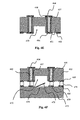
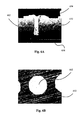
- the wire bonding technique is a popular technique for providing electrical interconnection, such as that employed in a conventional MEMS device 1 shown in Fig. 1A , in which a MEMS wafer 2 is bonded to a cap wafer 3 and a MEMS device 4 on the MEMS wafer 2 is connected to a solder ball 5 through a wire bond 6 which is held in a via 7 using an epoxy material 8.
- the wire bonding technique has limited application in MEMS packaging.
- ultra sonic energy applied in the frequency range between 50 and 100 kHz for performing wire bonding may stimulate the oscillation of the suspended mechanical structure of the MEMS device 4. This is because most MEMS devices have resonant frequency in the foregoing frequency range, thereby increasing the risk of failure during wire bonding.
- Through-wafer vias are typically intended for providing interconnects between both sides of wafers with which micro-devices are fabricated using WLP.
- Current packaging trend shows that vertical interconnects are favoured because of space efficiency and design simplicity, leading to the increased popularity of WLP devices.
- array sizes of devices for input/output (I/O) are limited when electrical connections are found at the periphery of the devices, primarily due to limited space along the edges of the devices for I/O leads. This limitation necessitates the use of through-wafer interconnects for micro-devices.
- a number of wafer-to-wafer bonding techniques have been developed for packaging micro-devices to achieve hermetic sealing. These techniques include silicon-to-glass anodic bonding, silicon-to-silicon fusion bonding, and wafer-to-wafer bonding using various intermediate materials as bonding media. Connections to a hermetically sealed micro-device are generally made under the bonding media against one of the wafers or through one of the wafer. Based on the foregoing preferences for vertical connections, through-wafer vias are thus favoured where hermetic sealing of micro-devices is an attendant requirement.
- One of the solutions for MEMS packaging can be to use electrically conductive through-wafer vias. These vias can be connected to metal conductors that connect to bond pads of the MEMS device. Such vias have advantages for space improvement and efficiency, and can be fabricated in a high volume-manufacturing method using bulk micromachining. For low I/O count devices, this method can be used without difficulty. For high I/O count micro-devices, however, this option can be a technical challenge.
- a method of fabricating a microcap 10 with vias 26/28 defined on a cap wafer 24 is proposed.
- the vias 26/28 are initially etched as trenches or wells and are filled by a conductive material from the top or the side of the cap wafer 24 having the trenches before the cap wafer 24 is bonded with a MEMS device wafer 12 to provide hermetic sealing.
- the cap wafer 24 is later thinned by backgrinding the non-trench side of the cap wafer 24 to expose the conductive vias 26/28.
- conductive vias which are made of semiconductor materials like Polysilicon, III-V materials or etc, which results in higher series resistance due to conductive vias than metallized vias.
- This approach only works for trenches with narrow openings ( ⁇ 10um) but not for trenches with larger openings because a proportionately thicker conductive material needs to be deposited to fill-up the vias before subsequent process steps are performed. This further results in excessive material build-up that induces very high film stress in the cap wafer, from which the microcap 10 is formed, which is susceptible to breakage due to deep vias that are already formed in the cap wafer.
- This proposed method thus requires two seed metal laying processes, thereby making it an expensive process. Also, the thick seed metal layer 210 needs to be removed by backgrinding/CMP process.
- a limitation of this proposed method of forming through-wafer vias by performing double seed metal laying processes is that it is suitable only for shallow through-wafer vias ( ⁇ 150um) with narrow openings ( ⁇ 5um). This is because it takes a longer time to fill the through-wafer vias by evaporation and electroplating. In cases where larger vias (>5um) are used, a very thick electroplated metal is formed on one side by the time the via openings are fully closed. The thick metal thus formed induces high stress on the wafer 204 and may cause the wafer 204 to crack.
- the photoresist layer exposed by the through-wafer vias is then subjected to exposure and development through the through-wafer vias to form seed areas. Once the seed areas are formed, electroplating is performed to fill the through-wafer vias using these seed areas.
- a limitation of this proposed method is the attendant difficulty to perform wafer-to-wafer bonding effectively using the photoresist layer without having enough solvent content to keep the photoresist layer soft. Also, the exposure and development of the seed areas performed through the deep through-wafer vias is not effectively performed as the developer cannot clear the photoresist exposed by through-wafer vias which are deep (>100um).
- the two wafers may not have sufficient bond strength to withstand the shear force applied during the backgrinding process since the photoresist layer is not inherently suitable for bonding the two wafers.
- a wafer-level MEMS package and method therefore are provided hereinafter wherein a MEMS device is connected to bonding pads on a MEMS wafer.
- a peripheral pattern is patterned along with the bonding pads on the MEMS wafer to encompass the bonding pads and the MEMS device.
- a cap wafer is processed to form through-wafer vias in the cap wafer using an etching process.
- a metal layer is uniformly deposited on a sacrificial wafer that is bonded to the cap wafer and removed after the etching process.
- the metal layer is uniformly deposited on the cap wafer before the via-etching process to serve as an etch-stop layer in an etching process.
- the cap wafer is formed in a way such that the through-wafer vias can be aligned with the bond pads of the MEMS wafer.
- the metal layer serves as a seed metal.
- the through-wafer vias are filled with a conductive material.
- the metal layer can also be an Under-Bump Metal (UBM) layer, which can be patterned to form bond pads and a peripheral pattern congruous with the corresponding bonding pads and peripheral pattern on the MEMS wafer for providing interconnection between the two wafers and a gasket for providing hermetic sealing, respectively.
- UBM Under-Bump Metal
- the bonding of the two wafers is performed before the via-etching process, which then requires electroless plating of the through-wafer vias after etching.
- the side of the cap wafer with the through-wafer vias exposed is now metallized with a UBM layer from which bond pads are patterned.
- Solder patterns are formed on the bond pads by conventional methods like screen printing or solder film deposition, lithography and etch before the wafer stack is finally singulated to form a surface mountable wafer-level MEMS package.
- a method for forming wafers having through-wafer vias for wafer-level packaging of devices comprising the steps of forming a metal layer on one of a first wafer and a second wafer; bonding the first wafer and the second wafer using the metal layer formed on one of the first wafer and the second wafer; forming a through-wafer via in one of the first wafer and the second wafer, the at least one metal layer being used for providing an etch stop layer at which etching of the through-wafer via stops; filling the through-wafer via with a conductive material, the at least one metal layer being used for providing an electroplate; the method characterized in that: the conductive material (362, 462, 562) fills the through-wafer via (354, 454, 554) by one of electroplating and electroless plating, and the through-wafer via (354, 454, 554) being formed on a first side of the cap
- Embodiments of the invention are described hereinafter for addressing the foregoing need to provide an alternative to conventional wafer-level packaging for micro-devices.
- a MEMS device is connected to bonding pads on a MEMS wafer.
- a peripheral pattern is patterned along with the bonding pads on the MEMS wafer to encompass the bonding pads and the MEMS device.
- a cap wafer is processed to form through-wafer vias in the cap wafer using an etching process.
- a metal layer is uniformly deposited on a sacrificial wafer that is bonded to the cap wafer and removed after the etching process.
- the metal layer is uniformly deposited on the cap wafer before the via-etching process to serve as an etch-stop layer in an etching process.
- the cap wafer is formed in a way such that the through-wafer vias can be aligned with the bond pads of the MEMS wafer.
- the metal layer serves as a seed metal. By means of an electroplating process and using the seed metal, the through-wafer vias are filled with a conductive material.
- the metal layer can also be an Under-Bump Metal (UBM) layer, which can be patterned to form bond pads and a peripheral pattern congruous with the corresponding bonding pads and peripheral pattern on the MEMS wafer for providing interconnection between the two wafers and a gasket for providing hermetic sealing, respectively.
- UBM Under-Bump Metal
- the two wafers are then aligned and eutectically bonded to form a wafer stack.
- the bonding of the two wafers is performed before the via-etching process, which then requires electroless plating of the through-wafer vias after etching.
- the side of the cap wafer with the through-wafer vias exposed is now metallized with a UBM layer from which bond pads are patterned. Solder bumps are placed on the bond pads before the wafer stack is finally singulated to form a surface mountable wafer-level MEMS package.
- a wafer-level MEMS package can be achieved with >400um through-wafer vias in the microcap of the MEMS package. This is attributed to deep through-wafer via filling processes described hereinafter.
- a yet further advantage relates to the high conductivity through-wafer vias for use in RF applications in which copper vias are appropriately used.
- a still further advantage relates to the reduction of the size of the MEMS package to a chip-scale MEMS package.
- An even further advantage relates to the absence of wafer thinning processes after the through-wafer vias are filled with conductive material.
- a wafer-level MEMS packaging method and a wafer-level MEMS package.
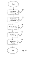
- the wafer-level MEMS packaging method is described while with reference to Figs 3B to 3G , the processing of the wafer-level MEMS package is described.
- a Via Etching step 302 a cap wafer 352 is processed in which through-wafer vias 354 are etched using conventional etching process including DRIE or the like etching processes.
- a barrier layer 356/357 for example comprising a suitable silicon oxide barrier 356 and/or a metal barrier 357 like Titanium or Tantalum, depending on the application and specific requirement, is then formed at the interface between the cap wafer 352 and the fill material for the through-wafer vias 354 using conventional barrier deposition or lithography and etching processes.
- the oxide barrier 356 provides insulation while the metal barrier 357 provides adhesion between the fill material and the through-wafer vias 354 and prevents diffusion of the fill material into the cap wafer 352.
- a seed film 359 can also be deposited on the side of the cap wafer 352 to be bonded with another wafer for facilitating improved bonding between the two wafers.
- the presence of the metal barrier 357 also provides adhesion between the cap wafer 352 and the seed film 359.
- the aspect ratio of the through-wafer vias 354 can be high (>10) and the depth of the through-wafer vias 354, and thus the thickness of the cap wafer 352, can be >400um, this does not limit the application of the embodiments of the invention to cap wafers and through-wafer vias of other dimensions.
- a seed layer 358 is deposited on a sacrificial wafer 360.
- the seed layer 358 can be a metal such as gold (Au) or copper (Cu), which also acts as a bonding layer for thermocompression or the like compression process.
- a metal barrier 359 comprising of Titanium or Tantalum can be deposited on the sacrificial wafer 360 for providing adhesion between the seed layer 358 and the sacrificial wafer 360.
- thermocompression or the like compression process is applied to the cap wafer 352 and the sacrificial wafer 360 with the seed layer 358 sandwiched therebetween.
- Conventional thermocompression settings optimised for the proper bonding of the two wafers are preferably used in this case.
- the Via Etching step 302 may be performed after the Seed Layer Deposition step 304 and the Wafers Bonding step 306.
- the seed layer 358 also acts as an etch-stop layer at which the etching of the through-wafer vias 354 stop.
- an electroplating process with the seed layer 358 acting as the electroplate is performed in which an electrolyte such as copper sulphate or the like electrolyte fills the through-wafer vias 354.
- an electrolyte such as copper sulphate or the like electrolyte fills the through-wafer vias 354.
- a conductive material 362, such as copper (Cu), gold (Au) or nickel (Ni) is left to fill the through-wafer vias 354 forming vertical interconnects.
- the barrier layer 356/357 acts as a barrier preventing transmigration or diffusion of the conductive material 362 into the cap wafer 352.
- the sacrificial wafer 360 is removed by conventional processes such as backgrinding and/or polishing.
- the seed layer 358 is also removed by the same backgrinding and/or polishing processes, thereby exposing the conductive material 362.
- the side of the cap wafer 352 opposite the seed layer 358 is also backgrinded and/or polished to expose the conductive material 362.
- UBM layers are deposited on both sides of the cap wafer 352 and patterned to form interconnect pads 364 and 366, which are electrically interconnected via the conductive material 362, and bond pads 368 to facilitate bonding and stacking the cap wafer 352 with a wafer containing a MEMS device.
- the deposition and patterning of the UBM layers are performed using conventional techniques, which are followed by the etching of a MEMS cavity 370 on the same side of the cap wafer 352 having the bond pads 368.
- the cap wafer 352 is solder bonded to a MEMS wafer 372 having a MEMS device 374 with a movable structure 376 using solder patterns 378, which are formed by conventional processes such as screen printing or lithography and etch, to form a wafer stack.
- Signals and electrical supply to the MEMS device 374 are conveyed to the MEMS device 374 via MEMS pads 379 formed on the MEMS wafer 372, which are congruent with and connected to the interconnect pads 366 on the cap wafer 352 using the solder patterns 378 on the cap wafer 352.
- bond pads 380 formed on the MEMS wafer 372 are also congruent with and connected to the bond pads 368 formed on the cap wafer 352.
- the MEMS cavity 370 is congruent with the MEMS device 374 when superposed over the MEMS device 374 so that the movement of the movable structure 376 is unimpeded within the MEMS cavity 370.
- the cap wafer 352 may be bonded to the MEMS wafer 372 using a bonding material such as metal or solder suitable for thermocompression or the like compression processes instead of the solder balls 378.
- solder bumps are applied to the interconnect pads 364 by conventional processes such as screen printing or lithography and etch, and the wafer stack singulated.
- solder bumps may be formed directly in place of the interconnect pads 364 formed during the Cap Wafer Processing step 310 by switching the electroplating solution and/or process after the electroplating process in the Via Electroplating step 308 to appropriately apply the solder bumps.
- FIG. 4A With reference to Figs. 4A to 4F , other embodiments of the invention are described for a wafer-level MEMS packaging method and a wafer-level MEMS package.
- the wafer-level MEMS packaging method is described while with reference to Figs 4B to 4F , the processing of the wafer-level MEMS package is described.
- a seed layer 458 is deposited on a cap wafer 452.
- the seed layer 458 can be a metal such as gold (Au) or copper (CU).
- an UBM layer 458 can be deposited, which can be titanium (Ti), nickel (Ni) or gold (Au). If the seed layer 358 is deposited on the cap wafer 452, the seed layer 458 has to be removed after electroplating to fill the through-wafer vias 454 in the cap wafer 452 with a conductive material 462. Otherwise, the UBM layer 458 can be left on the cap wafer 452 for subsequent patterning to form pads on the cap wafer 452. Before the seed layer 458 is deposited on the cap wafer 452, a metal barrier 457 comprising of Titanium or Tantalum can be deposited on the cap wafer 452 for providing adhesion between the seed layer 458 and the cap wafer 452.
- the cap wafer 452 is processed in which the through-wafer vias 454 are etched using conventional etching process including DRIE or the like etching processes.
- a barrier layer 456/457 for example comprising a suitable silicon oxide barrier 456 and/or a metal barrier 457 like Titanium or Tantalum, depending on the application and specific requirement, is formed at the interface between the cap wafer 452 and the fill material for the through-wafer vias 454 using conventional barrier deposition or lithography and etching processes.
- the oxide barrier 456 provides insulation while the metal barrier 457 provides adhesion between the fill material and the through-wafer vias 454 and prevents diffusion of the fill material into the cap wafer 452.
- the aspect ratio of the through-wafer vias 454 can be high (>10) and the depth of the through-wafer vias 454, and thus the thickness of the cap wafer 452, can be >400um.
- the seed layer or UBM layer 458 also acts as an etch-stop layer at which the etching of the through-wafer vias 454 stop.
- an electroplating process with the seed layer or UBM layer 458 acting as the electroplate is performed in which an electrolyte such as copper sulphate or the like electrolyte fills the through-wafer vias 454.
- an electrolyte such as copper sulphate or the like electrolyte fills the through-wafer vias 454.
- a conductive material 462 such as copper (Cu), gold (Au) or nickel (Ni)
- the barrier layer 456 acts as a barrier preventing transmigration or diffusion of the conductive material 462 into the cap wafer 452.
- a Cap Wafer Processing step 408 if the seed layer 458 is not a UBM layer 458, then the seed layer 458 is removed by the conventional backgrinding and/or polishing processes, thereby exposing the conductive material 462.
- the side of the cap wafer 452 opposite the seed layer 458 is also backgrinded and/or polished to expose the conductive material 462.
- UBM layers are deposited on both sides of the cap wafer 452 and patterned to form interconnect pads 464 and 466, which are electrically interconnected via the conductive material 462, and bond pads 468 to facilitate bonding and stacking the cap wafer 452 with a MEMS wafer 472.
- the deposition and patterning of the UBM layers are performed using conventional techniques, which are followed by the etching of a MEMS cavity 470 on the same side of the cap wafer 452 having the bond pads 468.
- the seed layer 458 is a UBM layer 458, then the UBM layer 458 is left on the cap wafer 452 and patterned accordingly to form the interconnect pads 466 and the bond pads 468.
- the cap wafer 452 is solder bonded to the MEMS wafer 472 having a MEMS device 474 with a movable structure 476 using solder patterns 478 to form a wafer stack.
- Signals and electrical supply to the MEMS device 474 are conveyed to the MEMS device 474 via MEMS pads 479 formed on the MEMS wafer 472, which are congruent with and connected to the interconnect pads 466 on the cap wafer 452 using the solder patterns 478.
- bond pads 480 formed on the MEMS wafer 472 are also congruent with and connected to the bond pads 468 formed on the cap wafer 452.
- the MEMS cavity 470 is congruent with the MEMS device 474 when superposed over the MEMS device 474 so that the movement of the movable structure 476 is unimpeded within the MEMS cavity 470.
- the cap wafer 452 may be bonded to the MEMS wafer 472 using a bonding material such as metal or solder suitable for thermocompression or the like compression processes instead of the solder balls 378.
- solder bumps are applied to the interconnect pads 464 and the wafer stack singulated.
- solder bumps may be formed directly in place of the interconnect pads 464 formed during the Cap Wafer Processing step 408 by switching the electroplating solution and/or process after the electroplating process in the Via Electroplating step 406 to appropriately apply the solder bumps.
- FIG. 5A With reference to Figs. 5A to 5F , further embodiments of the invention are described for a wafer-level MEMS packaging method and a wafer-level MEMS package.
- the wafer-level MEMS packaging method is described while with reference to Figs 5B to 5F , the processing of the wafer-level MEMS package is described.
- a UBM layer is deposited on a cap wafer 552 and subsequently patterned to form interconnect pads 566 and bond pads 568.
- a layer of bonding material such as metal or solder is also deposited after the UBM layer and similarly patterned to form bonding patches 582.
- the bonding patches 582 are congruent with the interconnect pads 566 and the bond pads 568.
- the deposition and patterning of the UBM layer and the bonding layer are performed using conventional techniques, which are followed by the etching of a MEMS cavity 570 on the same side of the cap wafer 552 having the bond pads 568.
- the interconnect pads 566 serve to provide connection with MEMS pads 579 prepared on a MEMS wafer 572 and convey signals and electrical supply to a MEMS device 574 on the MEMS wafer 572 via the MEMS pads 579.
- the interconnect pads 566 through vertical interconnects in the cap wafer 552 in turn convey the signals and electrical supply outside the MEMS package.
- Such vertical interconnects are to be formed in the cap wafer 552 after the formation of through-hole vias 554 in the cap wafer 552 in a subsequent step.
- the bond pads 568 facilitate the bonding and stacking of the cap wafer 552 with a MEMS wafer 572.
- the MEMS pads 579 for the MEMS device 572 with a movable structure 576 and bond pads 580 are formed on the MEMS wafer 572.
- the MEMS pads 579 are congruent with the interconnect pads 566 on the cap wafer 552.
- the bond pads 580 formed on the MEMS wafer 572 are also congruent with the bond pads 568 formed on the cap wafer 552.
- the cap wafer 552 is bonded to the MEMS wafer 572 using thermocompression or the like compression processes to form a wafer stack.
- the MEMS pads 579 formed on the MEMS wafer 572, which are congruent with the interconnect pads 566 on the cap wafer 552, and the bond pads 580 formed on the MEMS wafer 572, which are also congruent with the bond pads 568 formed on the cap wafer 552, are bonded via the application of thermocompression on the bonding patches 568.
- the MEMS cavity 570 is congruent with the MEMS device 574 when superposed over the MEMS device 574 so that the movement of the movable structure 576 is unimpeded within the MEMS cavity 570.
- the cap wafer 552 may be bonded to the MEMS wafer 572 by a eutectic method such as solder-to-metal or metal-to-metal bonding instead of bonding patches 568.
- the cap wafer 552 is processed in which lithographically patterning is performed and the through-wafer vias 554 are etched using conventional etching process including DRIE or the like etching processes.
- the through-wafer vias 554 are formed in congruence with the interconnect pads 566.
- a barrier layer 556/557 for example comprising a suitable silicon oxide barrier and/or a metal barrier like Titanium or Tantalum, depending on the application and specific requirement, is formed at the interface between the cap wafer 552 and the fill material for the through-wafer vias 554 using conventional barrier deposition or lithography and etching processes.
- the oxide barrier provides insulation while the metal barrier provides adhesion between the fill material and the through-wafer vias 554 and prevents diffusion of the fill material into the cap wafer 552.
- the aspect ratio of the through-wafer vias 554 can be high (>10) and the depth of the through-wafer vias 554, and thus the thickness of the cap wafer 552, can be >400um.
- the interconnect pads 566 act as an etch-stop layer at which the etching of the through-wafer vias 554 stop.
- an electroless plating process is performed to fill the through-wafer vias 554 with a conductive material 562 such as copper (Cu), gold (Au) or nickel (Ni), for forming the vertical interconnects.
- the electroless plating process is performed using conventional processes.
- solder bumps are formed over the filled through-wafer vias 554 by switching the electroplating solution and/or process after the electroplating process in the Via Electroplating step 508 to appropriately apply the solder bumps and the wafer stack singulated.
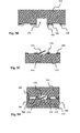
- an experiment of a process of etching through-wafer vias in a cap wafer and subsequently filling these with metal by an electroplating process is conducted with the following conditions:
- a through-wafer via 662 of 400 um depth in a wafer 652 after copper electroplating process from a seed layer is achieved.
- Minimal build-up 684 is created during the formation of the through-wafer via 662, which after backgrinding is flushed and therefore provides good planarity for the subsequent deposition of a pad or a solder bump.
- any sacrificial wafer and the seed layer is removed by wafer grinding and polishing processes.
- Fig. 6B shows the through-wafer via 662 after backgrinding and polishing.
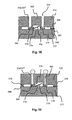
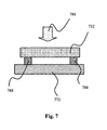
- a cap wafer 752 and a MEMS wafer 772 may through thermocompression or the like compression processes 786 be hermetically sealed if a hermetically sealing material, such as Frit glass, is used in place of the solder balls 378/478 or the bonding patches 582 used in the foregoing embodiments.
- a hermetically sealing material such as Frit glass
- the bonding pads 368/380/468/480/568/589 used in the foregoing embodiments have to be continuous pads encompassing the MEMS pads 379/479/579 so that when bonded therebetween using the hermetically sealing material form a gasket around the MEMS device.
- wafer-level packaging for micro-devices is described.
- the foregoing wafer-level packaging methods may be applied to a 3-dimensional or 3-D package in which carrier wafers having micro-devices are stacked and a micro-device on one carrier wafer depends on through-wafer vias of adjacent carrier wafers to convey signals and electrical supply. Therefore instead of processing cap wafers, the wafer-level packaging may be applied to carrier wafers containing micro-devices.
Landscapes
- Engineering & Computer Science (AREA)
- Microelectronics & Electronic Packaging (AREA)
- Computer Hardware Design (AREA)
- Physics & Mathematics (AREA)
- Condensed Matter Physics & Semiconductors (AREA)
- General Physics & Mathematics (AREA)
- Manufacturing & Machinery (AREA)
- Power Engineering (AREA)
- Micromachines (AREA)
- Internal Circuitry In Semiconductor Integrated Circuit Devices (AREA)
- Hybrid Cells (AREA)
- Packaging Frangible Articles (AREA)
Claims (20)
- Verfahren zur Ausbildung von Wafern mit Waferdurchkontaktierungen für die Herstellung von Wafer-L.evel-Packages für Vorrichtungen, umfassend die folgenden Schritte:Ausbilden wenigstens einer Metallschicht (358, 458, 566) auf einem die Deckplatte bildenden Wafer (352, 452, 552) oder einem die Trägerplatte bildenden Wafer (360, 472, 572), um den die Deckplatte bildenden Wafer (352, 452, 552) und den die Trägerplatte bildenden Wafer (360, 472, 572) durch Bonden miteinander zu verbinden,Verbinden des die Deckplatte bildenden Wafers (352, 452, 552) und des die Trägerplatte bildenden Wafers (360, 472, 572) durch bonding mit Hilfe der wenigstens einen auf dem die Deckplatte bildenden Wafer (352, 452, 552) oder dem die Trägerplatte bildenden Wafer (360, 472, 572) ausgebildeten Metallschicht (358, 458, 566),Ausbilden von Waferdurchkontaktierungen (354, 454, 554) in dem die Deckplatte bildenden Wafer (352, 452, 552), wobei die wenigstens eine Metallschicht (358, 458, 566) dazu dient, eine Ätzstopschicht bereitzustellen, an der das Ätzen der Waferdurchkontaktierungen (354, 454, 554) endet,Füllen der Waferdurchkontaktierung (354, 454, 554) mit einem leitenden Material (362, 462, 562), wobei die wenigstens eine Metallschicht (358, 458, 566) dazu dient, während der elektrolytischen Metallabscheidung einen galvanischen Überzug bereitzustellen, undAusbilden einer Kavität (370, 470, 570) in dem die Deckplatte bildenden Wafer (352, 452, 552),wobei das Verfahren dadurch gekennzeichnet ist, dass
das leitende Material (362, 462, 562) die Waferdurchkontaktierung (354, 454, 554) durch elektrolytisches oder stromloses Metallabscheiden füllt, und die Waferdurchkontaktierung (354, 454, 554) auf einer ersten Seite des die Deckplatte bildenden Wafers (352, 452, 552) ausgebildet wird, und der die Deckplatte bildende Wafer (352, 452, 552) der die Kavität (370, 470, 570) auf einer zweiten Seite desselben ausbildet, mit dem die Trägerplatte bildenden Wafer (360, 472, 572) auf der zweiten Seite, der ersten Seite gegenüberliegend, verbunden wird. - Verfahren nach Anspruch 1, ferner folgenden Schritt umfassend:Ausbilden der Kavität in dem die Deckplatte bildenden Wafer oder dem die Trägerplatte bildenden Wafer, der die Waferdurchkontaktierung aufweist,wobei die Kavität eine Vorrichtung überdecken kann.
- Verfahren nach Anspruch 2, wobei der Schritt des Ausbildens der Kavität den Schritt umfasst, die Kavität zum Überdecken einer MEMS-Vorrichtung auszubilden.
- Verfahren nach Anspruch 3, wobei der Schritt des Ausbildens der Kavität ferner den Schritt umfasst, einen wesentlichen Zwischenraum auszubilden um eine ungehinderte Bewegung einer beweglichen Konstruktion der MEMS-Vorrichtung zu ermöglichen.
- Verfahren nach Anspruch 2, wobei der Schritt des Verbindens des die Deckplatte bildenden Wafers und des die Trägerplatte bildenden Wafers nach dem Schritt des Ausbildens der Waferdurchkontaktierung in dem die Deckplatte oder dem die Trägerplatte bildenden Wafer erfolgt.
- Verfahren nach Anspruch 5, wobei der Schritt des Ausbildens der Waferdurchkontaktierung auf einem der Wafer aus dem die Deckplatte bildenden Wafer und dem die Trägerplatte bildenden Wafer erfolgt und der Schritt des Ausbildens der wenigstens einen Metallschicht auf dem anderen Wafer aus dem die Deckplatte bildenden Wafer und dem die Trägerplatte bildenden Wafer erfolgt, wobei es sich bei dem anderen Wafer aus dem die Deckplatte bildenden Wafer und dem die Trägerplatte bildenden Wafer um einen Opfer-Wafer handelt.
- Verfahren nach Anspruch 6, ferner den Schritt des Entfernens des Opfer-Wafers umfassend, wobei dieser nach dem Schritt des Füllens der Waferdurchkontaktierung erfolgt.
- Verfahren nach Anspruch 5, wobei der Schritt des Ausbildens der Waferdurchkontaktierung und der wenigstens einen Metallschicht auf dem gleichen Wafer aus dem die Deckplatte bildenden Wafer und dem die Trägerplatte bildenden Wafer erfolgt.
- Verfahren nach Anspruch 8, wobei der Schritt des Ausbildens der Kavität den Schritt umfasst, die Kavität zum Überdecken der Vorrichtung in dem anderen Wafer aus dem die Deckplatte bildenden Wafer und dem die Trägerplatte bildenden Wafer auszubilden, der die Waferdurchkontaktierung aufweist.
- Verfahren nach Anspruch 1, wobei der Schritt des Ausbildens der Waferdurchkontaktierung den Schritt umfasst, die Waferdurchkontaktierung in den die Deckplatte bildenden Wafer oder den die Trägerplatte bildenden Wafer zu ätzen.
- Verfahren nach Anspruch 1, wobei der Schritt des Ausbildens der Kavität den Schritt umfasst, die Kavität in den Wafer aus dem die Deckplatte bildenden Wafer und dem die Trägerplatte bildenden Wafer zu ätzen, welcher die Waferdurchkontaktierung aufweist.
- Verfahren nach Anspruch 1, wobei der Schritt des Verbindens des die Deckplatte bildenden Wafers und des die Trägerplatte bildenden Wafers den Schritt umfasst, den die Deckplatte bildenden Wafer und den die Trägerplatte bildenden Wafer mittels Thermokompressionstechnik mit Hilfe einer mit der Waferdurchkontaktierung verbundenen bonding-Fläche zu verbinden.
- Verfahren nach Anspruch 1, wobei der Schritt des Füllens der Waferdurchkontaktierung den Schritt umfasst, die Waferdurchkontaktierung durch Galvanisieren mit einem Metall zu füllen.
- Verfahren nach Anspruch 1, wobei der Schritt des Ausbildens der wenigstens einen Metallschicht den Schritt umfasst, eine Metallkeimschicht auf dem die Deckplatte bildenden Wafer oder dem die Trägerplatte bildenden Wafer abzuscheiden.
- Verfahren nach Anspruch 2, wobei der Schritt des Verbindens des die Deckplatte bildenden Wafers und des die Trägerplatte bildenden Wafers vor dem Schritt des Ausbildens der Waferdurchkontaktierung in dem die Deckplatte oder die Trägerplatte bildenden Wafer erfolgt,
- Verfahren nach Anspruch 15, wobei der Schritt des Ausbildens der Waferdurchkontaktierung auf einem der Wafer aus dem die Deckplatte bildenden Wafer und dem die Trägerplatte bildenden Wafer erfolgt und der Schritt des Ausbildens der wenigstens einen Metallschicht auf dem anderen Wafer aus dem die Deckplatte bildenden Wafer und dem die Trägerplatte bildenden Wafer erfolgt, wobei es sich bei dem anderen Wafer aus dem die Deckplatte bildenden Wafer und dem die Trägerplatte bildenden Wafer um einen Opfer-Wafer handelt.
- Verfahren nach Anspruch 16, ferner den Schritt des Entfernens des Opfer-Wafers umfassend, wobei dieser nach dem Schritt des Füllens der Waferdurchkontaktierung erfolgt.
- Verfahren nach Anspruch 15. wobei der Schritt des Ausbildens der Waferdurchkontaktierung und der wenigstens einen Metallschicht auf dem gleichen Wafer aus dem die Deckplatte bildenden Wafer und dem die Trägerplatte bildenden Wafer erfolgt.
- Verfahren nach Anspruch 18, wobei der Schritt des Ausbildens der Kavität den Schritt umfasst, die Kavität zum Überdecken der Vorrichtung in dem anderen Wafer aus dem die Deckplatte bildenden Wafer und dem die Trägerplatte bildenden Wafer auszubilden, der die Waferdurchkontaktierung aufweist.
- Verfahren nach Anspruch 1, wobei der Schritt des Ausbildens der Waferdurchkontaktierung den Schritt umfasst, die Waferdurchkontaktierung in einem Trägerwafer auszubilden, welcher eine Vorrichtung enthält, um ein dreidimensionales Paket durch Übereinanderschichten von wenigstens zwei Trägerwafern bereitzustellen,
Applications Claiming Priority (2)
| Application Number | Priority Date | Filing Date | Title |
|---|---|---|---|
| SG200206388A SG111972A1 (en) | 2002-10-17 | 2002-10-17 | Wafer-level package for micro-electro-mechanical systems |
| SG200206388 | 2002-10-17 |
Publications (3)
| Publication Number | Publication Date |
|---|---|
| EP1415950A2 EP1415950A2 (de) | 2004-05-06 |
| EP1415950A3 EP1415950A3 (de) | 2005-02-02 |
| EP1415950B1 true EP1415950B1 (de) | 2008-05-28 |
Family
ID=32091979
Family Applications (1)
| Application Number | Title | Priority Date | Filing Date |
|---|---|---|---|
| EP03256508A Expired - Lifetime EP1415950B1 (de) | 2002-10-17 | 2003-10-15 | Verpackung auf Waferebene für mikroelektromechanische Vorrichtungen |
Country Status (5)
| Country | Link |
|---|---|
| US (1) | US6846725B2 (de) |
| EP (1) | EP1415950B1 (de) |
| AT (1) | ATE396955T1 (de) |
| DE (1) | DE60321287D1 (de) |
| SG (1) | SG111972A1 (de) |
Cited By (14)
| Publication number | Priority date | Publication date | Assignee | Title |
|---|---|---|---|---|
| US7482272B2 (en) | 2005-06-14 | 2009-01-27 | John Trezza | Through chip connection |
| US7521806B2 (en) | 2005-06-14 | 2009-04-21 | John Trezza | Chip spanning connection |
| US7534722B2 (en) | 2005-06-14 | 2009-05-19 | John Trezza | Back-to-front via process |
| US7560813B2 (en) | 2005-06-14 | 2009-07-14 | John Trezza | Chip-based thermo-stack |
| US7659202B2 (en) | 2005-06-14 | 2010-02-09 | John Trezza | Triaxial through-chip connection |
| US7670874B2 (en) | 2007-02-16 | 2010-03-02 | John Trezza | Plated pillar package formation |
| US7687397B2 (en) | 2006-06-06 | 2010-03-30 | John Trezza | Front-end processed wafer having through-chip connections |
| US7687400B2 (en) | 2005-06-14 | 2010-03-30 | John Trezza | Side stacking apparatus and method |
| US7781886B2 (en) | 2005-06-14 | 2010-08-24 | John Trezza | Electronic chip contact structure |
| US7786592B2 (en) | 2005-06-14 | 2010-08-31 | John Trezza | Chip capacitive coupling |
| US7838997B2 (en) | 2005-06-14 | 2010-11-23 | John Trezza | Remote chip attachment |
| US7851348B2 (en) | 2005-06-14 | 2010-12-14 | Abhay Misra | Routingless chip architecture |
| US8456015B2 (en) | 2005-06-14 | 2013-06-04 | Cufer Asset Ltd. L.L.C. | Triaxial through-chip connection |
| US10833016B2 (en) | 2017-05-31 | 2020-11-10 | International Business Machines Corporation | Semiconductor device including superconducting metal through-silicon-vias and method of making the same |
Families Citing this family (144)
| Publication number | Priority date | Publication date | Assignee | Title |
|---|---|---|---|---|
| JP2004247530A (ja) * | 2003-02-14 | 2004-09-02 | Renesas Technology Corp | 半導体装置及びその製造方法 |
| ITTO20030269A1 (it) * | 2003-04-08 | 2004-10-09 | St Microelectronics Srl | Procedimento per la fabbricazione di un dispositivo |
| US7350060B2 (en) | 2003-04-24 | 2008-03-25 | International Business Machines Corporation | Method and apparatus for sending thread-execution-state-sensitive supervisory commands to a simultaneous multi-threaded (SMT) processor |
| TWI275168B (en) * | 2003-06-06 | 2007-03-01 | Sanyo Electric Co | Semiconductor device and method for making the same |
| US7368808B2 (en) * | 2003-06-30 | 2008-05-06 | Intel Corporation | MEMS packaging using a non-silicon substrate for encapsulation and interconnection |
| US20050054133A1 (en) * | 2003-09-08 | 2005-03-10 | Felton Lawrence E. | Wafer level capped sensor |
| US7275424B2 (en) * | 2003-09-08 | 2007-10-02 | Analog Devices, Inc. | Wafer level capped sensor |
| KR100541087B1 (ko) * | 2003-10-01 | 2006-01-10 | 삼성전기주식회사 | 마이크로 디바이스를 위한 웨이퍼 레벨 패키지 및 제조방법 |
| US7091124B2 (en) | 2003-11-13 | 2006-08-15 | Micron Technology, Inc. | Methods for forming vias in microelectronic devices, and methods for packaging microelectronic devices |
| US8084866B2 (en) | 2003-12-10 | 2011-12-27 | Micron Technology, Inc. | Microelectronic devices and methods for filling vias in microelectronic devices |
| US6936918B2 (en) * | 2003-12-15 | 2005-08-30 | Analog Devices, Inc. | MEMS device with conductive path through substrate |
| US7291513B2 (en) * | 2003-12-15 | 2007-11-06 | Dalsa Semiconductor Inc. | Hermetic wafer-level packaging for MEMS devices with low-temperature metallurgy |
| US20050170609A1 (en) * | 2003-12-15 | 2005-08-04 | Alie Susan A. | Conductive bond for through-wafer interconnect |
| US20050247894A1 (en) | 2004-05-05 | 2005-11-10 | Watkins Charles M | Systems and methods for forming apertures in microfeature workpieces |
| US7262509B2 (en) * | 2004-05-11 | 2007-08-28 | Intel Corporation | Microelectronic assembly having a perimeter around a MEMS device |
| US7608534B2 (en) * | 2004-06-02 | 2009-10-27 | Analog Devices, Inc. | Interconnection of through-wafer vias using bridge structures |
| US7232754B2 (en) | 2004-06-29 | 2007-06-19 | Micron Technology, Inc. | Microelectronic devices and methods for forming interconnects in microelectronic devices |
| JP2006024653A (ja) * | 2004-07-06 | 2006-01-26 | Tokyo Electron Ltd | 貫通基板および貫通基板の製造方法 |
| WO2006004128A1 (ja) | 2004-07-06 | 2006-01-12 | Tokyo Electron Limited | 貫通基板およびインターポーザ、ならびに貫通基板の製造方法 |
| KR100594716B1 (ko) * | 2004-07-27 | 2006-06-30 | 삼성전자주식회사 | 공동부를 구비한 캡 웨이퍼, 이를 이용한 반도체 칩, 및그 제조방법 |
| SG120200A1 (en) | 2004-08-27 | 2006-03-28 | Micron Technology Inc | Slanted vias for electrical circuits on circuit boards and other substrates |
| US7109068B2 (en) * | 2004-08-31 | 2006-09-19 | Micron Technology, Inc. | Through-substrate interconnect fabrication methods |
| US7300857B2 (en) | 2004-09-02 | 2007-11-27 | Micron Technology, Inc. | Through-wafer interconnects for photoimager and memory wafers |
| KR100618343B1 (ko) * | 2004-10-28 | 2006-08-31 | 삼성전자주식회사 | 패키징 기판의 제조방법 및 이를 이용한 패키징 방법. |
| US8237256B2 (en) * | 2004-12-10 | 2012-08-07 | Ipdia | Integrated package |
| TWI449134B (zh) * | 2004-12-10 | 2014-08-11 | 恩智浦股份有限公司 | 積體封裝 |
| US7271482B2 (en) | 2004-12-30 | 2007-09-18 | Micron Technology, Inc. | Methods for forming interconnects in microelectronic workpieces and microelectronic workpieces formed using such methods |
| KR100594952B1 (ko) * | 2005-02-04 | 2006-06-30 | 삼성전자주식회사 | 웨이퍼 레벨 패키징 캡 및 그 제조방법 |
| US7276794B2 (en) * | 2005-03-02 | 2007-10-02 | Endevco Corporation | Junction-isolated vias |
| US7553695B2 (en) * | 2005-03-17 | 2009-06-30 | Hymite A/S | Method of fabricating a package for a micro component |
| US20060211233A1 (en) * | 2005-03-21 | 2006-09-21 | Skyworks Solutions, Inc. | Method for fabricating a wafer level package having through wafer vias for external package connectivity and related structure |
| US7287687B2 (en) * | 2005-03-22 | 2007-10-30 | I.C.A.R.D., L.L.C. | System and method for regulating alcohol consumption |
| US7576426B2 (en) * | 2005-04-01 | 2009-08-18 | Skyworks Solutions, Inc. | Wafer level package including a device wafer integrated with a passive component |
| US7371676B2 (en) * | 2005-04-08 | 2008-05-13 | Micron Technology, Inc. | Method for fabricating semiconductor components with through wire interconnects |
| US20060252254A1 (en) * | 2005-05-06 | 2006-11-09 | Basol Bulent M | Filling deep and wide openings with defect-free conductor |
| WO2006124597A2 (en) * | 2005-05-12 | 2006-11-23 | Foster Ron B | Infinitely stackable interconnect device and method |
| US7393770B2 (en) * | 2005-05-19 | 2008-07-01 | Micron Technology, Inc. | Backside method for fabricating semiconductor components with conductive interconnects |
| US20060278996A1 (en) * | 2005-06-14 | 2006-12-14 | John Trezza | Active packaging |
| WO2006138492A2 (en) * | 2005-06-14 | 2006-12-28 | Cubic Wafer, Inc. | Post & penetration interconnection |
| US7807550B2 (en) * | 2005-06-17 | 2010-10-05 | Dalsa Semiconductor Inc. | Method of making MEMS wafers |
| CN101213429B (zh) * | 2005-06-27 | 2012-02-08 | Hl-平面技术有限公司 | 用于检测电磁波的器件以及生产这样的器件的方法 |
| US7795134B2 (en) | 2005-06-28 | 2010-09-14 | Micron Technology, Inc. | Conductive interconnect structures and formation methods using supercritical fluids |
| US7608470B2 (en) * | 2005-06-28 | 2009-10-27 | Intel Corporation | Interconnection device including one or more embedded vias and method of producing the same |
| US20070004079A1 (en) * | 2005-06-30 | 2007-01-04 | Geefay Frank S | Method for making contact through via contact to an offset contactor inside a cap for the wafer level packaging of FBAR chips |
| US7429529B2 (en) * | 2005-08-05 | 2008-09-30 | Farnworth Warren M | Methods of forming through-wafer interconnects and structures resulting therefrom |
| US7517798B2 (en) * | 2005-09-01 | 2009-04-14 | Micron Technology, Inc. | Methods for forming through-wafer interconnects and structures resulting therefrom |
| US7262134B2 (en) | 2005-09-01 | 2007-08-28 | Micron Technology, Inc. | Microfeature workpieces and methods for forming interconnects in microfeature workpieces |
| US7622377B2 (en) | 2005-09-01 | 2009-11-24 | Micron Technology, Inc. | Microfeature workpiece substrates having through-substrate vias, and associated methods of formation |
| US7863187B2 (en) | 2005-09-01 | 2011-01-04 | Micron Technology, Inc. | Microfeature workpieces and methods for forming interconnects in microfeature workpieces |
| US20070103009A1 (en) * | 2005-10-31 | 2007-05-10 | Xiao (Charles) Yang | Method and Structure for Integrated Energy Storage Device |
| US7491567B2 (en) * | 2005-11-22 | 2009-02-17 | Honeywell International Inc. | MEMS device packaging methods |
| KR100705007B1 (ko) * | 2005-11-30 | 2007-04-09 | 매그나칩 반도체 유한회사 | 마이크로 센서 및 그 제조방법 |
| US7307348B2 (en) * | 2005-12-07 | 2007-12-11 | Micron Technology, Inc. | Semiconductor components having through wire interconnects (TWI) |
| KR100721625B1 (ko) * | 2005-12-21 | 2007-05-23 | 매그나칩 반도체 유한회사 | Mems 패키지 및 그 제조방법 |
| KR101231243B1 (ko) * | 2005-12-21 | 2013-02-08 | 매그나칩 반도체 유한회사 | Mems 패키지 및 그 제조방법 |
| US7696083B2 (en) * | 2006-03-10 | 2010-04-13 | Endeoco Corporation | Multi-layer device |
| US7625814B2 (en) * | 2006-03-29 | 2009-12-01 | Asm Nutool, Inc. | Filling deep features with conductors in semiconductor manufacturing |
| US7485561B2 (en) * | 2006-03-29 | 2009-02-03 | Asm Nutool, Inc. | Filling deep features with conductors in semiconductor manufacturing |
| US7659612B2 (en) | 2006-04-24 | 2010-02-09 | Micron Technology, Inc. | Semiconductor components having encapsulated through wire interconnects (TWI) |
| US7749899B2 (en) | 2006-06-01 | 2010-07-06 | Micron Technology, Inc. | Microelectronic workpieces and methods and systems for forming interconnects in microelectronic workpieces |
| US20070281460A1 (en) * | 2006-06-06 | 2007-12-06 | Cubic Wafer, Inc. | Front-end processed wafer having through-chip connections |
| KR100846569B1 (ko) * | 2006-06-14 | 2008-07-15 | 매그나칩 반도체 유한회사 | Mems 소자의 패키지 및 그 제조방법 |
| US8022554B2 (en) | 2006-06-15 | 2011-09-20 | Sitime Corporation | Stacked die package for MEMS resonator system |
| US7635606B2 (en) * | 2006-08-02 | 2009-12-22 | Skyworks Solutions, Inc. | Wafer level package with cavities for active devices |
| US7629249B2 (en) | 2006-08-28 | 2009-12-08 | Micron Technology, Inc. | Microfeature workpieces having conductive interconnect structures formed by chemically reactive processes, and associated systems and methods |
| US8021981B2 (en) | 2006-08-30 | 2011-09-20 | Micron Technology, Inc. | Redistribution layers for microfeature workpieces, and associated systems and methods |
| US7902643B2 (en) | 2006-08-31 | 2011-03-08 | Micron Technology, Inc. | Microfeature workpieces having interconnects and conductive backplanes, and associated systems and methods |
| US7820233B2 (en) * | 2006-09-27 | 2010-10-26 | Unimicron Technology Corp. | Method for fabricating a flip chip substrate structure |
| US20080087979A1 (en) * | 2006-10-13 | 2008-04-17 | Analog Devices, Inc. | Integrated Circuit with Back Side Conductive Paths |
| EP2074647B1 (de) | 2006-10-17 | 2012-10-10 | Cufer Asset Ltd. L.L.C. | Waferdurchgangslochbildung |
| US7851331B2 (en) * | 2006-11-27 | 2010-12-14 | Taiwan Semiconductor Manufacturing Co., Ltd. | Bonding structures and methods of forming bonding structures |
| US7812459B2 (en) * | 2006-12-19 | 2010-10-12 | Taiwan Semiconductor Manufacturing Company, Ltd. | Three-dimensional integrated circuits with protection layers |
| US7642657B2 (en) * | 2006-12-21 | 2010-01-05 | Analog Devices, Inc. | Stacked MEMS device |
| US7705613B2 (en) | 2007-01-03 | 2010-04-27 | Abhay Misra | Sensitivity capacitive sensor |
| JP4807272B2 (ja) * | 2007-02-05 | 2011-11-02 | パナソニック電工株式会社 | 半導体ウェハへの貫通孔配線の形成方法 |
| US7705632B2 (en) | 2007-02-15 | 2010-04-27 | Wyman Theodore J Ted | Variable off-chip drive |
| US7803693B2 (en) | 2007-02-15 | 2010-09-28 | John Trezza | Bowed wafer hybridization compensation |
| US7598163B2 (en) | 2007-02-15 | 2009-10-06 | John Callahan | Post-seed deposition process |
| US20080217708A1 (en) * | 2007-03-09 | 2008-09-11 | Skyworks Solutions, Inc. | Integrated passive cap in a system-in-package |
| US20080237048A1 (en) * | 2007-03-30 | 2008-10-02 | Ismail Emesh | Method and apparatus for selective electrofilling of through-wafer vias |
| US7850060B2 (en) | 2007-04-05 | 2010-12-14 | John Trezza | Heat cycle-able connection |
| US7748116B2 (en) | 2007-04-05 | 2010-07-06 | John Trezza | Mobile binding in an electronic connection |
| US7960210B2 (en) | 2007-04-23 | 2011-06-14 | Cufer Asset Ltd. L.L.C. | Ultra-thin chip packaging |
| DE102007019638A1 (de) | 2007-04-26 | 2008-10-30 | Robert Bosch Gmbh | Verfahren zur Herstellung eines mikromechanischen Bauelements mit Trenchstruktur zur Rückseitenkontaktierung |
| KR100951284B1 (ko) * | 2007-06-01 | 2010-04-02 | 삼성전기주식회사 | 웨이퍼 레벨 패키지 제조방법 |
| US20090029152A1 (en) * | 2007-07-25 | 2009-01-29 | Analog Devices, Inc. | Wafer Bonding Using Nanoparticle Material |
| SG150410A1 (en) | 2007-08-31 | 2009-03-30 | Micron Technology Inc | Partitioned through-layer via and associated systems and methods |
| US20090065365A1 (en) * | 2007-09-11 | 2009-03-12 | Asm Nutool, Inc. | Method and apparatus for copper electroplating |
| TWI336313B (en) * | 2007-10-17 | 2011-01-21 | Pixart Imaging Inc | Microelectromechanical device and method for making same |
| KR20150068495A (ko) | 2007-11-30 | 2015-06-19 | 스카이워크스 솔루션즈, 인코포레이티드 | 플립 칩 실장을 이용하는 웨이퍼 레벨 패키징 |
| US7884015B2 (en) | 2007-12-06 | 2011-02-08 | Micron Technology, Inc. | Methods for forming interconnects in microelectronic workpieces and microelectronic workpieces formed using such methods |
| DE102007060632A1 (de) * | 2007-12-17 | 2009-06-18 | Robert Bosch Gmbh | Verfahren zum Herstellen eines Kappenwafers für einen Sensor |
| US8900931B2 (en) * | 2007-12-26 | 2014-12-02 | Skyworks Solutions, Inc. | In-situ cavity integrated circuit package |
| KR20090109969A (ko) * | 2008-04-17 | 2009-10-21 | 한국전자통신연구원 | 웨이퍼 레벨 패키지 및 그 제조 방법 |
| US7872332B2 (en) | 2008-09-11 | 2011-01-18 | Micron Technology, Inc. | Interconnect structures for stacked dies, including penetrating structures for through-silicon vias, and associated systems and methods |
| US8030780B2 (en) | 2008-10-16 | 2011-10-04 | Micron Technology, Inc. | Semiconductor substrates with unitary vias and via terminals, and associated systems and methods |
| JP5246103B2 (ja) * | 2008-10-16 | 2013-07-24 | 大日本印刷株式会社 | 貫通電極基板の製造方法 |
| SE534510C2 (sv) | 2008-11-19 | 2011-09-13 | Silex Microsystems Ab | Funktionell inkapsling |
| US7884016B2 (en) * | 2009-02-12 | 2011-02-08 | Asm International, N.V. | Liner materials and related processes for 3-D integration |
| US8604603B2 (en) * | 2009-02-20 | 2013-12-10 | The Hong Kong University Of Science And Technology | Apparatus having thermal-enhanced and cost-effective 3D IC integration structure with through silicon via interposers |
| US9057853B2 (en) * | 2009-02-20 | 2015-06-16 | The Hong Kong University Of Science And Technology | Apparatus having an embedded 3D hybrid integration for optoelectronic interconnects |
| US8315793B2 (en) * | 2009-06-03 | 2012-11-20 | Honeywell International Inc. | Integrated micro-electro-mechanical systems (MEMS) sensor device |
| TWI509757B (zh) * | 2009-08-03 | 2015-11-21 | Pixart Imaging Inc | 微機電系統晶片及其封裝方法 |
| TWI502705B (zh) * | 2009-08-19 | 2015-10-01 | 精材科技股份有限公司 | 晶片封裝體及其製造方法 |
| US7989246B2 (en) * | 2009-09-11 | 2011-08-02 | Pixart Imaging Incorporation | Package method of micro-electro-mechanical system chip |
| US8729695B2 (en) * | 2009-09-25 | 2014-05-20 | Agency For Science, Technology And Research | Wafer level package and a method of forming a wafer level package |
| US8138062B2 (en) * | 2009-12-15 | 2012-03-20 | Freescale Semiconductor, Inc. | Electrical coupling of wafer structures |
| TWI397157B (zh) | 2009-12-28 | 2013-05-21 | 矽品精密工業股份有限公司 | 具微機電元件之封裝結構及其製法 |
| TWI395312B (zh) * | 2010-01-20 | 2013-05-01 | 矽品精密工業股份有限公司 | 具微機電元件之封裝結構及其製法 |
| US8304863B2 (en) | 2010-02-09 | 2012-11-06 | International Business Machines Corporation | Electromigration immune through-substrate vias |
| JP5155352B2 (ja) * | 2010-03-25 | 2013-03-06 | 日本電波工業株式会社 | 圧電デバイス |
| US7985659B1 (en) * | 2010-03-31 | 2011-07-26 | Freescale Semiconductor, Inc. | Semiconductor device with a controlled cavity and method of formation |
| TWI455265B (zh) * | 2010-11-01 | 2014-10-01 | 矽品精密工業股份有限公司 | 具微機電元件之封裝結構及其製法 |
| TWI455266B (zh) | 2010-12-17 | 2014-10-01 | 矽品精密工業股份有限公司 | 具微機電元件之封裝結構及其製法 |
| US8674518B2 (en) * | 2011-01-03 | 2014-03-18 | Shu-Ming Chang | Chip package and method for forming the same |
| US8754507B2 (en) | 2011-01-18 | 2014-06-17 | Hong Kong Applied Science and Technology Research Institute Company Limited | Forming through-silicon-vias for multi-wafer integrated circuits |
| US8368152B2 (en) * | 2011-04-18 | 2013-02-05 | Taiwan Semiconductor Manufacturing Company, Ltd. | MEMS device etch stop |
| CN102751266B (zh) * | 2011-04-21 | 2016-02-03 | 精材科技股份有限公司 | 芯片封装体及其形成方法 |
| TW201250947A (en) | 2011-05-12 | 2012-12-16 | Siliconware Precision Industries Co Ltd | Package structure having a micromechanical electronic component and method of making same |
| US8824706B2 (en) | 2011-08-30 | 2014-09-02 | Qualcomm Mems Technologies, Inc. | Piezoelectric microphone fabricated on glass |
| US8724832B2 (en) | 2011-08-30 | 2014-05-13 | Qualcomm Mems Technologies, Inc. | Piezoelectric microphone fabricated on glass |
| US8698258B2 (en) * | 2011-09-30 | 2014-04-15 | General Electric Company | 3D integrated electronic device structure including increased thermal dissipation capabilities |
| CN102363520B (zh) * | 2011-11-04 | 2014-04-09 | 中国科学院半导体研究所 | 用于微机电系统器件的圆片级三维封装方法 |
| US8811636B2 (en) | 2011-11-29 | 2014-08-19 | Qualcomm Mems Technologies, Inc. | Microspeaker with piezoelectric, metal and dielectric membrane |
| DE102012210033B4 (de) * | 2012-06-14 | 2023-02-02 | Robert Bosch Gmbh | Bauelement mit Durchkontaktierung und Verfahren zur Herstellung |
| ITTO20120827A1 (it) | 2012-09-24 | 2014-03-25 | St Microelectronics Srl | Incapsulamento a livello di fetta di un dispositivo integrato mems e relativo procedimento di fabbricazione |
| SE537869C2 (sv) * | 2012-11-01 | 2015-11-03 | Silex Microsystems Ab | Substratgenomgående vior |
| US9758372B1 (en) * | 2013-02-13 | 2017-09-12 | Amkor Technology, Inc. | MEMS package with MEMS die, magnet, and window substrate fabrication method and structure |
| US9177929B2 (en) * | 2013-05-16 | 2015-11-03 | National Center For Advanced Packaging Co., Ltd. | Techniques for fabricating fine-pitch micro-bumps |
| US9676611B2 (en) | 2013-10-18 | 2017-06-13 | Nxp Usa, Inc. | Sensor device packages and related fabrication methods |
| US9768147B2 (en) * | 2014-02-03 | 2017-09-19 | Micron Technology, Inc. | Thermal pads between stacked semiconductor dies and associated systems and methods |
| US10442685B2 (en) | 2014-03-31 | 2019-10-15 | Nxp Usa, Inc. | Microelectronic packages having hermetic cavities and methods for the production thereof |
| US9891244B2 (en) | 2014-08-15 | 2018-02-13 | Nxp Usa, Inc. | Microelectronic packages having split gyroscope structures and methods for the fabrication thereof |
| US9720696B2 (en) | 2014-09-30 | 2017-08-01 | International Business Machines Corporation | Independent mapping of threads |
| US10133576B2 (en) | 2015-01-13 | 2018-11-20 | International Business Machines Corporation | Parallel slice processor having a recirculating load-store queue for fast deallocation of issue queue entries |
| US9971970B1 (en) * | 2015-04-27 | 2018-05-15 | Rigetti & Co, Inc. | Microwave integrated quantum circuits with VIAS and methods for making the same |
| JP6350759B2 (ja) * | 2015-08-18 | 2018-07-04 | 三菱電機株式会社 | 半導体装置 |
| US10641975B2 (en) * | 2015-09-03 | 2020-05-05 | Telefonaktiebolaget Lm Ericsson (Publ) | System, method, and apparatus for optical broadcast transmission in a circuit board |
| US20170240418A1 (en) * | 2016-02-18 | 2017-08-24 | Knowles Electronics, Llc | Low-cost miniature mems vibration sensor |
| JP2017199854A (ja) | 2016-04-28 | 2017-11-02 | Tdk株式会社 | 貫通配線基板 |
| US11121301B1 (en) | 2017-06-19 | 2021-09-14 | Rigetti & Co, Inc. | Microwave integrated quantum circuits with cap wafers and their methods of manufacture |
| CN110164782A (zh) | 2018-02-13 | 2019-08-23 | 财团法人工业技术研究院 | 封装结构及组件连接的方法 |
| US11220423B2 (en) * | 2018-11-01 | 2022-01-11 | Invensense, Inc. | Reduced MEMS cavity gap |
| CN111137839A (zh) * | 2020-01-14 | 2020-05-12 | 清华大学 | 用于面内运动式微机电系统器件的三维圆片级封装结构 |
Family Cites Families (5)
| Publication number | Priority date | Publication date | Assignee | Title |
|---|---|---|---|---|
| US5448014A (en) * | 1993-01-27 | 1995-09-05 | Trw Inc. | Mass simultaneous sealing and electrical connection of electronic devices |
| JP3303791B2 (ja) * | 1998-09-02 | 2002-07-22 | 株式会社村田製作所 | 電子部品の製造方法 |
| US6228675B1 (en) * | 1999-07-23 | 2001-05-08 | Agilent Technologies, Inc. | Microcap wafer-level package with vias |
| US6770503B1 (en) * | 1999-10-21 | 2004-08-03 | The Charles Stark Draper Laboratory, Inc. | Integrated packaging of micromechanical sensors and associated control circuits |
| ATE354814T1 (de) * | 2000-08-03 | 2007-03-15 | Texas Instruments Inc | Vereinzelte die-wafer mit mikrospiegeln |
-
2002
- 2002-10-17 SG SG200206388A patent/SG111972A1/en unknown
-
2003
- 2003-01-27 US US10/351,534 patent/US6846725B2/en not_active Expired - Fee Related
- 2003-10-15 EP EP03256508A patent/EP1415950B1/de not_active Expired - Lifetime
- 2003-10-15 DE DE60321287T patent/DE60321287D1/de not_active Expired - Lifetime
- 2003-10-15 AT AT03256508T patent/ATE396955T1/de not_active IP Right Cessation
Cited By (41)
| Publication number | Priority date | Publication date | Assignee | Title |
|---|---|---|---|---|
| US7932584B2 (en) | 2005-06-14 | 2011-04-26 | Cufer Asset Ltd. L.L.C. | Stacked chip-based system and method |
| US7942182B2 (en) | 2005-06-14 | 2011-05-17 | Cufer Asset Ltd. L.L.C. | Rigid-backed, membrane-based chip tooling |
| US7534722B2 (en) | 2005-06-14 | 2009-05-19 | John Trezza | Back-to-front via process |
| US7538033B2 (en) | 2005-06-14 | 2009-05-26 | John Trezza | Post-attachment chip-to-chip connection |
| US7560813B2 (en) | 2005-06-14 | 2009-07-14 | John Trezza | Chip-based thermo-stack |
| US7659202B2 (en) | 2005-06-14 | 2010-02-09 | John Trezza | Triaxial through-chip connection |
| US9324629B2 (en) | 2005-06-14 | 2016-04-26 | Cufer Asset Ltd. L.L.C. | Tooling for coupling multiple electronic chips |
| US9147635B2 (en) | 2005-06-14 | 2015-09-29 | Cufer Asset Ltd. L.L.C. | Contact-based encapsulation |
| US7687400B2 (en) | 2005-06-14 | 2010-03-30 | John Trezza | Side stacking apparatus and method |
| US7767493B2 (en) | 2005-06-14 | 2010-08-03 | John Trezza | Post & penetration interconnection |
| US7781886B2 (en) | 2005-06-14 | 2010-08-24 | John Trezza | Electronic chip contact structure |
| US7785987B2 (en) | 2005-06-14 | 2010-08-31 | John Trezza | Isolating chip-to-chip contact |
| US7786592B2 (en) | 2005-06-14 | 2010-08-31 | John Trezza | Chip capacitive coupling |
| US7785931B2 (en) | 2005-06-14 | 2010-08-31 | John Trezza | Chip-based thermo-stack |
| US7808111B2 (en) | 2005-06-14 | 2010-10-05 | John Trezza | Processed wafer via |
| US7838997B2 (en) | 2005-06-14 | 2010-11-23 | John Trezza | Remote chip attachment |
| US7847412B2 (en) | 2005-06-14 | 2010-12-07 | John Trezza | Isolating chip-to-chip contact |
| US7851348B2 (en) | 2005-06-14 | 2010-12-14 | Abhay Misra | Routingless chip architecture |
| US7884483B2 (en) | 2005-06-14 | 2011-02-08 | Cufer Asset Ltd. L.L.C. | Chip connector |
| US7919870B2 (en) | 2005-06-14 | 2011-04-05 | Cufer Asset Ltd. L.L.C. | Coaxial through chip connection |
| US7521806B2 (en) | 2005-06-14 | 2009-04-21 | John Trezza | Chip spanning connection |
| US7946331B2 (en) | 2005-06-14 | 2011-05-24 | Cufer Asset Ltd. L.L.C. | Pin-type chip tooling |
| US7482272B2 (en) | 2005-06-14 | 2009-01-27 | John Trezza | Through chip connection |
| US7969015B2 (en) | 2005-06-14 | 2011-06-28 | Cufer Asset Ltd. L.L.C. | Inverse chip connector |
| US7989958B2 (en) | 2005-06-14 | 2011-08-02 | Cufer Assett Ltd. L.L.C. | Patterned contact |
| US8021922B2 (en) | 2005-06-14 | 2011-09-20 | Cufer Asset Ltd. L.L.C. | Remote chip attachment |
| US8053903B2 (en) | 2005-06-14 | 2011-11-08 | Cufer Asset Ltd. L.L.C. | Chip capacitive coupling |
| US8067312B2 (en) | 2005-06-14 | 2011-11-29 | Cufer Asset Ltd. L.L.C. | Coaxial through chip connection |
| US8084851B2 (en) | 2005-06-14 | 2011-12-27 | Cufer Asset Ltd. L.L.C. | Side stacking apparatus and method |
| US8093729B2 (en) | 2005-06-14 | 2012-01-10 | Cufer Asset Ltd. L.L.C. | Electrically conductive interconnect system and method |
| US8154131B2 (en) | 2005-06-14 | 2012-04-10 | Cufer Asset Ltd. L.L.C. | Profiled contact |
| US8197626B2 (en) | 2005-06-14 | 2012-06-12 | Cufer Asset Ltd. L.L.C. | Rigid-backed, membrane-based chip tooling |
| US8197627B2 (en) | 2005-06-14 | 2012-06-12 | Cufer Asset Ltd. L.L.C. | Pin-type chip tooling |
| US8232194B2 (en) | 2005-06-14 | 2012-07-31 | Cufer Asset Ltd. L.L.C. | Process for chip capacitive coupling |
| US8283778B2 (en) | 2005-06-14 | 2012-10-09 | Cufer Asset Ltd. L.L.C. | Thermally balanced via |
| US8456015B2 (en) | 2005-06-14 | 2013-06-04 | Cufer Asset Ltd. L.L.C. | Triaxial through-chip connection |
| US8643186B2 (en) | 2005-06-14 | 2014-02-04 | Cufer Asset Ltd. L.L.C. | Processed wafer via |
| US8846445B2 (en) | 2005-06-14 | 2014-09-30 | Cufer Asset Ltd. L.L.C. | Inverse chip connector |
| US7687397B2 (en) | 2006-06-06 | 2010-03-30 | John Trezza | Front-end processed wafer having through-chip connections |
| US7670874B2 (en) | 2007-02-16 | 2010-03-02 | John Trezza | Plated pillar package formation |
| US10833016B2 (en) | 2017-05-31 | 2020-11-10 | International Business Machines Corporation | Semiconductor device including superconducting metal through-silicon-vias and method of making the same |
Also Published As
| Publication number | Publication date |
|---|---|
| SG111972A1 (en) | 2005-06-29 |
| EP1415950A2 (de) | 2004-05-06 |
| US6846725B2 (en) | 2005-01-25 |
| ATE396955T1 (de) | 2008-06-15 |
| DE60321287D1 (de) | 2008-07-10 |
| US20040077154A1 (en) | 2004-04-22 |
| EP1415950A3 (de) | 2005-02-02 |
Similar Documents
| Publication | Publication Date | Title |
|---|---|---|
| EP1415950B1 (de) | Verpackung auf Waferebene für mikroelektromechanische Vorrichtungen | |
| JP5189491B2 (ja) | ウェハ・レベル・パッケージングの方法 | |
| US6376280B1 (en) | Microcap wafer-level package | |
| CN101189180B (zh) | 用于微部件的薄封装 | |
| US6429511B2 (en) | Microcap wafer-level package | |
| Ramm et al. | 3D integration technology: Status and application development | |
| KR100831405B1 (ko) | 웨이퍼 본딩 패키징 방법 | |
| EP2273545B1 (de) | Verfahren zur Einsatzverbindung sowie Montagekit zur Verwendung in dem Verfahren | |
| US20040259325A1 (en) | Wafer level chip scale hermetic package | |
| KR100851931B1 (ko) | 반도체 패키지용의 개선된 상호접속 구조 | |
| KR20170013343A (ko) | 2d 및 3d ic 패키징을 위한 통합된 인터포저 솔루션 | |
| WO2010104610A2 (en) | Stacked microelectronic assemblies having vias extending through bond pads | |
| EP3316283B1 (de) | Verfahren zur herstellung einer substratdurchkontaktierung | |
| EP1199744B1 (de) | Mikrodeckelgehäuse auf Scheibenebene | |
| Feil et al. | Ultra thin ICs and MEMS elements: techniques for wafer thinning, stress-free separation, assembly and interconnection | |
| CN115196583B (zh) | 一种mems传感器芯片与asic芯片的扇出型封装结构及封装方法 | |
| Schjølberg-Henriksen et al. | Miniaturised sensor node for tire pressure monitoring (e-CUBES) | |
| US11877518B2 (en) | Package for electric device and method of manufacturing the package | |
| Wang | Through‐substrate Vias | |
| HK1121731B (zh) | 用於微部件的薄封装 |
Legal Events
| Date | Code | Title | Description |
|---|---|---|---|
| PUAI | Public reference made under article 153(3) epc to a published international application that has entered the european phase |
Free format text: ORIGINAL CODE: 0009012 |
|
| AK | Designated contracting states |
Kind code of ref document: A2 Designated state(s): AT BE BG CH CY CZ DE DK EE ES FI FR GB GR HU IE IT LI LU MC NL PT RO SE SI SK TR |
|
| AX | Request for extension of the european patent |
Extension state: AL LT LV MK |
|
| PUAL | Search report despatched |
Free format text: ORIGINAL CODE: 0009013 |
|
| AK | Designated contracting states |
Kind code of ref document: A3 Designated state(s): AT BE BG CH CY CZ DE DK EE ES FI FR GB GR HU IE IT LI LU MC NL PT RO SE SI SK TR |
|
| AX | Request for extension of the european patent |
Extension state: AL LT LV MK |
|
| 17P | Request for examination filed |
Effective date: 20050729 |
|
| AKX | Designation fees paid |
Designated state(s): AT BE BG CH CY CZ DE DK EE ES FI FR GB GR HU IE IT LI LU MC NL PT RO SE SI SK TR |
|
| 17Q | First examination report despatched |
Effective date: 20060330 |
|
| 17Q | First examination report despatched |
Effective date: 20060330 |
|
| GRAP | Despatch of communication of intention to grant a patent |
Free format text: ORIGINAL CODE: EPIDOSNIGR1 |
|
| GRAS | Grant fee paid |
Free format text: ORIGINAL CODE: EPIDOSNIGR3 |
|
| GRAA | (expected) grant |
Free format text: ORIGINAL CODE: 0009210 |
|
| AK | Designated contracting states |
Kind code of ref document: B1 Designated state(s): AT BE BG CH CY CZ DE DK EE ES FI FR GB GR HU IE IT LI LU MC NL PT RO SE SI SK TR |
|
| REG | Reference to a national code |
Ref country code: GB Ref legal event code: FG4D |
|
| REG | Reference to a national code |
Ref country code: CH Ref legal event code: EP |
|
| REF | Corresponds to: |
Ref document number: 60321287 Country of ref document: DE Date of ref document: 20080710 Kind code of ref document: P |
|
| REG | Reference to a national code |
Ref country code: IE Ref legal event code: FG4D |
|
| PG25 | Lapsed in a contracting state [announced via postgrant information from national office to epo] |
Ref country code: SI Free format text: LAPSE BECAUSE OF FAILURE TO SUBMIT A TRANSLATION OF THE DESCRIPTION OR TO PAY THE FEE WITHIN THE PRESCRIBED TIME-LIMIT Effective date: 20080528 |
|
| PG25 | Lapsed in a contracting state [announced via postgrant information from national office to epo] |
Ref country code: FI Free format text: LAPSE BECAUSE OF FAILURE TO SUBMIT A TRANSLATION OF THE DESCRIPTION OR TO PAY THE FEE WITHIN THE PRESCRIBED TIME-LIMIT Effective date: 20080528 Ref country code: ES Free format text: LAPSE BECAUSE OF FAILURE TO SUBMIT A TRANSLATION OF THE DESCRIPTION OR TO PAY THE FEE WITHIN THE PRESCRIBED TIME-LIMIT Effective date: 20080908 |
|
| PG25 | Lapsed in a contracting state [announced via postgrant information from national office to epo] |
Ref country code: AT Free format text: LAPSE BECAUSE OF FAILURE TO SUBMIT A TRANSLATION OF THE DESCRIPTION OR TO PAY THE FEE WITHIN THE PRESCRIBED TIME-LIMIT Effective date: 20080528 Ref country code: NL Free format text: LAPSE BECAUSE OF FAILURE TO SUBMIT A TRANSLATION OF THE DESCRIPTION OR TO PAY THE FEE WITHIN THE PRESCRIBED TIME-LIMIT Effective date: 20080528 |
|
| NLV1 | Nl: lapsed or annulled due to failure to fulfill the requirements of art. 29p and 29m of the patents act | ||
| PG25 | Lapsed in a contracting state [announced via postgrant information from national office to epo] |
Ref country code: CZ Free format text: LAPSE BECAUSE OF FAILURE TO SUBMIT A TRANSLATION OF THE DESCRIPTION OR TO PAY THE FEE WITHIN THE PRESCRIBED TIME-LIMIT Effective date: 20080528 Ref country code: DK Free format text: LAPSE BECAUSE OF FAILURE TO SUBMIT A TRANSLATION OF THE DESCRIPTION OR TO PAY THE FEE WITHIN THE PRESCRIBED TIME-LIMIT Effective date: 20080528 Ref country code: SE Free format text: LAPSE BECAUSE OF FAILURE TO SUBMIT A TRANSLATION OF THE DESCRIPTION OR TO PAY THE FEE WITHIN THE PRESCRIBED TIME-LIMIT Effective date: 20080828 Ref country code: PT Free format text: LAPSE BECAUSE OF FAILURE TO SUBMIT A TRANSLATION OF THE DESCRIPTION OR TO PAY THE FEE WITHIN THE PRESCRIBED TIME-LIMIT Effective date: 20081028 |
|
| PG25 | Lapsed in a contracting state [announced via postgrant information from national office to epo] |
Ref country code: BE Free format text: LAPSE BECAUSE OF FAILURE TO SUBMIT A TRANSLATION OF THE DESCRIPTION OR TO PAY THE FEE WITHIN THE PRESCRIBED TIME-LIMIT Effective date: 20080528 Ref country code: SK Free format text: LAPSE BECAUSE OF FAILURE TO SUBMIT A TRANSLATION OF THE DESCRIPTION OR TO PAY THE FEE WITHIN THE PRESCRIBED TIME-LIMIT Effective date: 20080528 Ref country code: RO Free format text: LAPSE BECAUSE OF FAILURE TO SUBMIT A TRANSLATION OF THE DESCRIPTION OR TO PAY THE FEE WITHIN THE PRESCRIBED TIME-LIMIT Effective date: 20080528 |
|
| PLBE | No opposition filed within time limit |
Free format text: ORIGINAL CODE: 0009261 |
|
| STAA | Information on the status of an ep patent application or granted ep patent |
Free format text: STATUS: NO OPPOSITION FILED WITHIN TIME LIMIT |
|
| PG25 | Lapsed in a contracting state [announced via postgrant information from national office to epo] |
Ref country code: EE Free format text: LAPSE BECAUSE OF FAILURE TO SUBMIT A TRANSLATION OF THE DESCRIPTION OR TO PAY THE FEE WITHIN THE PRESCRIBED TIME-LIMIT Effective date: 20080528 Ref country code: BG Free format text: LAPSE BECAUSE OF FAILURE TO SUBMIT A TRANSLATION OF THE DESCRIPTION OR TO PAY THE FEE WITHIN THE PRESCRIBED TIME-LIMIT Effective date: 20080828 |
|
| 26N | No opposition filed |
Effective date: 20090303 |
|
| PG25 | Lapsed in a contracting state [announced via postgrant information from national office to epo] |
Ref country code: MC Free format text: LAPSE BECAUSE OF NON-PAYMENT OF DUE FEES Effective date: 20081031 |
|
| REG | Reference to a national code |
Ref country code: CH Ref legal event code: PL |
|
| PG25 | Lapsed in a contracting state [announced via postgrant information from national office to epo] |
Ref country code: IT Free format text: LAPSE BECAUSE OF FAILURE TO SUBMIT A TRANSLATION OF THE DESCRIPTION OR TO PAY THE FEE WITHIN THE PRESCRIBED TIME-LIMIT Effective date: 20080528 |
|
| PG25 | Lapsed in a contracting state [announced via postgrant information from national office to epo] |
Ref country code: LI Free format text: LAPSE BECAUSE OF NON-PAYMENT OF DUE FEES Effective date: 20081031 Ref country code: CH Free format text: LAPSE BECAUSE OF NON-PAYMENT OF DUE FEES Effective date: 20081031 Ref country code: IE Free format text: LAPSE BECAUSE OF NON-PAYMENT OF DUE FEES Effective date: 20081015 |
|
| PGFP | Annual fee paid to national office [announced via postgrant information from national office to epo] |
Ref country code: DE Payment date: 20091030 Year of fee payment: 7 |
|
| PGFP | Annual fee paid to national office [announced via postgrant information from national office to epo] |
Ref country code: FR Payment date: 20091112 Year of fee payment: 7 Ref country code: GB Payment date: 20091102 Year of fee payment: 7 |
|
| PG25 | Lapsed in a contracting state [announced via postgrant information from national office to epo] |
Ref country code: LU Free format text: LAPSE BECAUSE OF NON-PAYMENT OF DUE FEES Effective date: 20081015 Ref country code: HU Free format text: LAPSE BECAUSE OF FAILURE TO SUBMIT A TRANSLATION OF THE DESCRIPTION OR TO PAY THE FEE WITHIN THE PRESCRIBED TIME-LIMIT Effective date: 20081129 Ref country code: CY Free format text: LAPSE BECAUSE OF FAILURE TO SUBMIT A TRANSLATION OF THE DESCRIPTION OR TO PAY THE FEE WITHIN THE PRESCRIBED TIME-LIMIT Effective date: 20080528 |
|
| PG25 | Lapsed in a contracting state [announced via postgrant information from national office to epo] |
Ref country code: TR Free format text: LAPSE BECAUSE OF FAILURE TO SUBMIT A TRANSLATION OF THE DESCRIPTION OR TO PAY THE FEE WITHIN THE PRESCRIBED TIME-LIMIT Effective date: 20080528 |
|
| PG25 | Lapsed in a contracting state [announced via postgrant information from national office to epo] |
Ref country code: GR Free format text: LAPSE BECAUSE OF FAILURE TO SUBMIT A TRANSLATION OF THE DESCRIPTION OR TO PAY THE FEE WITHIN THE PRESCRIBED TIME-LIMIT Effective date: 20080829 |
|
| GBPC | Gb: european patent ceased through non-payment of renewal fee |
Effective date: 20101015 |
|
| PG25 | Lapsed in a contracting state [announced via postgrant information from national office to epo] |
Ref country code: FR Free format text: LAPSE BECAUSE OF NON-PAYMENT OF DUE FEES Effective date: 20101102 |
|
| REG | Reference to a national code |
Ref country code: FR Ref legal event code: ST Effective date: 20110630 |
|
| PG25 | Lapsed in a contracting state [announced via postgrant information from national office to epo] |
Ref country code: GB Free format text: LAPSE BECAUSE OF NON-PAYMENT OF DUE FEES Effective date: 20101015 |
|
| REG | Reference to a national code |
Ref country code: DE Ref legal event code: R119 Ref document number: 60321287 Country of ref document: DE Effective date: 20110502 |
|
| PG25 | Lapsed in a contracting state [announced via postgrant information from national office to epo] |
Ref country code: DE Free format text: LAPSE BECAUSE OF NON-PAYMENT OF DUE FEES Effective date: 20110502 |