EP1396875A2 - Inducteur en spirale 3-D empilé sur un substrat semiconducteur - Google Patents
Inducteur en spirale 3-D empilé sur un substrat semiconducteur Download PDFInfo
- Publication number
- EP1396875A2 EP1396875A2 EP03019916A EP03019916A EP1396875A2 EP 1396875 A2 EP1396875 A2 EP 1396875A2 EP 03019916 A EP03019916 A EP 03019916A EP 03019916 A EP03019916 A EP 03019916A EP 1396875 A2 EP1396875 A2 EP 1396875A2
- Authority
- EP
- European Patent Office
- Prior art keywords
- turn
- level
- dielectric layer
- turns
- over
- Prior art date
- Legal status (The legal status is an assumption and is not a legal conclusion. Google has not performed a legal analysis and makes no representation as to the accuracy of the status listed.)
- Granted
Links
- 239000000463 material Substances 0.000 title description 6
- 239000004065 semiconductor Substances 0.000 title description 3
- 239000000758 substrate Substances 0.000 claims abstract description 40
- 239000003989 dielectric material Substances 0.000 claims abstract description 3
- 239000004020 conductor Substances 0.000 claims description 28
- 238000000034 method Methods 0.000 claims description 15
- 238000012545 processing Methods 0.000 claims description 7
- 230000007423 decrease Effects 0.000 claims description 2
- 238000004519 manufacturing process Methods 0.000 claims description 2
- 239000010410 layer Substances 0.000 description 39
- XUIMIQQOPSSXEZ-UHFFFAOYSA-N Silicon Chemical compound [Si] XUIMIQQOPSSXEZ-UHFFFAOYSA-N 0.000 description 16
- 229910052710 silicon Inorganic materials 0.000 description 16
- 239000010703 silicon Substances 0.000 description 16
- 229910052751 metal Inorganic materials 0.000 description 7
- 239000002184 metal Substances 0.000 description 7
- VYPSYNLAJGMNEJ-UHFFFAOYSA-N Silicium dioxide Chemical compound O=[Si]=O VYPSYNLAJGMNEJ-UHFFFAOYSA-N 0.000 description 6
- 238000013461 design Methods 0.000 description 4
- 230000003071 parasitic effect Effects 0.000 description 4
- RYGMFSIKBFXOCR-UHFFFAOYSA-N Copper Chemical compound [Cu] RYGMFSIKBFXOCR-UHFFFAOYSA-N 0.000 description 3
- 230000015556 catabolic process Effects 0.000 description 3
- 229910052802 copper Inorganic materials 0.000 description 3
- 239000010949 copper Substances 0.000 description 3
- 238000006731 degradation reaction Methods 0.000 description 3
- 238000013459 approach Methods 0.000 description 2
- 230000015572 biosynthetic process Effects 0.000 description 2
- 230000000694 effects Effects 0.000 description 2
- 238000005516 engineering process Methods 0.000 description 2
- 230000004907 flux Effects 0.000 description 2
- 239000010931 gold Substances 0.000 description 2
- 239000011229 interlayer Substances 0.000 description 2
- 238000001465 metallisation Methods 0.000 description 2
- 238000012986 modification Methods 0.000 description 2
- 230000004048 modification Effects 0.000 description 2
- 238000011160 research Methods 0.000 description 2
- 235000012239 silicon dioxide Nutrition 0.000 description 2
- 239000000377 silicon dioxide Substances 0.000 description 2
- 229910052814 silicon oxide Inorganic materials 0.000 description 2
- 229910016570 AlCu Inorganic materials 0.000 description 1
- JBRZTFJDHDCESZ-UHFFFAOYSA-N AsGa Chemical compound [As]#[Ga] JBRZTFJDHDCESZ-UHFFFAOYSA-N 0.000 description 1
- 235000013290 Sagittaria latifolia Nutrition 0.000 description 1
- 229910052782 aluminium Inorganic materials 0.000 description 1
- XAGFODPZIPBFFR-UHFFFAOYSA-N aluminium Chemical compound [Al] XAGFODPZIPBFFR-UHFFFAOYSA-N 0.000 description 1
- WPPDFTBPZNZZRP-UHFFFAOYSA-N aluminum copper Chemical compound [Al].[Cu] WPPDFTBPZNZZRP-UHFFFAOYSA-N 0.000 description 1
- 235000015246 common arrowhead Nutrition 0.000 description 1
- 230000000295 complement effect Effects 0.000 description 1
- 230000001419 dependent effect Effects 0.000 description 1
- 238000000151 deposition Methods 0.000 description 1
- 230000008021 deposition Effects 0.000 description 1
- 238000011161 development Methods 0.000 description 1
- 238000005530 etching Methods 0.000 description 1
- PCHJSUWPFVWCPO-UHFFFAOYSA-N gold Chemical compound [Au] PCHJSUWPFVWCPO-UHFFFAOYSA-N 0.000 description 1
- 229910052737 gold Inorganic materials 0.000 description 1
- 230000007774 longterm Effects 0.000 description 1
- 229910044991 metal oxide Inorganic materials 0.000 description 1
- 150000004706 metal oxides Chemical class 0.000 description 1
- 150000002739 metals Chemical class 0.000 description 1
- 238000010295 mobile communication Methods 0.000 description 1
- 238000005457 optimization Methods 0.000 description 1
- 238000004806 packaging method and process Methods 0.000 description 1
- 238000000206 photolithography Methods 0.000 description 1
- 229920002120 photoresistant polymer Polymers 0.000 description 1
Images
Classifications
-
- H—ELECTRICITY
- H01—ELECTRIC ELEMENTS
- H01L—SEMICONDUCTOR DEVICES NOT COVERED BY CLASS H10
- H01L28/00—Passive two-terminal components without a potential-jump or surface barrier for integrated circuits; Details thereof; Multistep manufacturing processes therefor
- H01L28/10—Inductors
-
- H—ELECTRICITY
- H01—ELECTRIC ELEMENTS
- H01L—SEMICONDUCTOR DEVICES NOT COVERED BY CLASS H10
- H01L27/00—Devices consisting of a plurality of semiconductor or other solid-state components formed in or on a common substrate
- H01L27/02—Devices consisting of a plurality of semiconductor or other solid-state components formed in or on a common substrate including semiconductor components specially adapted for rectifying, oscillating, amplifying or switching and having potential barriers; including integrated passive circuit elements having potential barriers
- H01L27/04—Devices consisting of a plurality of semiconductor or other solid-state components formed in or on a common substrate including semiconductor components specially adapted for rectifying, oscillating, amplifying or switching and having potential barriers; including integrated passive circuit elements having potential barriers the substrate being a semiconductor body
- H01L27/08—Devices consisting of a plurality of semiconductor or other solid-state components formed in or on a common substrate including semiconductor components specially adapted for rectifying, oscillating, amplifying or switching and having potential barriers; including integrated passive circuit elements having potential barriers the substrate being a semiconductor body including only semiconductor components of a single kind
-
- Y—GENERAL TAGGING OF NEW TECHNOLOGICAL DEVELOPMENTS; GENERAL TAGGING OF CROSS-SECTIONAL TECHNOLOGIES SPANNING OVER SEVERAL SECTIONS OF THE IPC; TECHNICAL SUBJECTS COVERED BY FORMER USPC CROSS-REFERENCE ART COLLECTIONS [XRACs] AND DIGESTS
- Y10—TECHNICAL SUBJECTS COVERED BY FORMER USPC
- Y10T—TECHNICAL SUBJECTS COVERED BY FORMER US CLASSIFICATION
- Y10T29/00—Metal working
- Y10T29/49—Method of mechanical manufacture
- Y10T29/49002—Electrical device making
- Y10T29/4902—Electromagnet, transformer or inductor
- Y10T29/49021—Magnetic recording reproducing transducer [e.g., tape head, core, etc.]
- Y10T29/49032—Fabricating head structure or component thereof
- Y10T29/4906—Providing winding
-
- Y—GENERAL TAGGING OF NEW TECHNOLOGICAL DEVELOPMENTS; GENERAL TAGGING OF CROSS-SECTIONAL TECHNOLOGIES SPANNING OVER SEVERAL SECTIONS OF THE IPC; TECHNICAL SUBJECTS COVERED BY FORMER USPC CROSS-REFERENCE ART COLLECTIONS [XRACs] AND DIGESTS
- Y10—TECHNICAL SUBJECTS COVERED BY FORMER USPC
- Y10T—TECHNICAL SUBJECTS COVERED BY FORMER US CLASSIFICATION
- Y10T29/00—Metal working
- Y10T29/49—Method of mechanical manufacture
- Y10T29/49002—Electrical device making
- Y10T29/4902—Electromagnet, transformer or inductor
- Y10T29/49073—Electromagnet, transformer or inductor by assembling coil and core
-
- Y—GENERAL TAGGING OF NEW TECHNOLOGICAL DEVELOPMENTS; GENERAL TAGGING OF CROSS-SECTIONAL TECHNOLOGIES SPANNING OVER SEVERAL SECTIONS OF THE IPC; TECHNICAL SUBJECTS COVERED BY FORMER USPC CROSS-REFERENCE ART COLLECTIONS [XRACs] AND DIGESTS
- Y10—TECHNICAL SUBJECTS COVERED BY FORMER USPC
- Y10T—TECHNICAL SUBJECTS COVERED BY FORMER US CLASSIFICATION
- Y10T29/00—Metal working
- Y10T29/49—Method of mechanical manufacture
- Y10T29/49002—Electrical device making
- Y10T29/49117—Conductor or circuit manufacturing
- Y10T29/49124—On flat or curved insulated base, e.g., printed circuit, etc.
- Y10T29/49155—Manufacturing circuit on or in base
- Y10T29/49165—Manufacturing circuit on or in base by forming conductive walled aperture in base
Definitions
- the present invention relates generally to integrated circuits and more particularly to on-chip silicon-based inductors.
- CMOS complementary metal oxide semiconductor
- AlCu aluminum-copper
- an active inductor In an active inductor high Q factor and inductance can be achieved in a really small silicon area. However, such approach suffers from high power consumption and high noise levels that are not acceptable for low power and high frequency applications. In addition, performance of active inductors are very sensitive and dependent upon the inductor's biasing circuitry, making it time consuming and tedious to design.
- the simplest and most commonly used on-chip inductors are planar silicon-based spiral inductors, which require careful layout optimization techniques to improve performance.
- the inductor is planar and fabricated on a conductive silicon substrate.
- the top metal is usually stacked with a few layers of lower metal through vias to minimize the overall metal series resistance. Nevertheless, when more layers are used to realize a very thick conductor, the whole spiral is brought closer to the substrate. This increases the spiral-to-substrate parasitic capacitance and hence results in a degradation of Q factor as well as the inductor's self-resonant frequency. It has been observed that the Q factor of a 4-layer stacked inductor decreases at a much faster rate compared to 1- to 3-layer stacked inductors. Because of this, it becomes extremely difficult to design high performance inductors with large inductance values since such a phenomenon is more pronounced when the inductors occupy large areas.
- the basic working principal is to minimize undesirable magnetic flux created by the induced substrate eddy current, especially at the inductor's core. This can be easily accomplished by reducing current density of the inductor's inner turns. Meanwhile, when current density of the inner turns is reduced, induced substrate current at the center of the inductor will also have a lower current density. As a result, at the inductor's core, parasitic magnetic flux generated in the substrate is much weaker and this helps increase the inductance and the Q factor of spiral inductors.
- the present invention provides a 3-D spiral stacked inductor having a substrate with a plurality of turns in a plurality of levels wherein the number of levels increases from an inner turn to the outer turns of the inductor.
- First and second connecting portions are respectively connected to an inner turn and an outermost turn, and a dielectric material contains the first and second connecting portions and the plurality of turns over the substrate. This will reduce current in the inner turn and lower current density in the outer turns to improve inductance and Q factor beyond 2.5 GHz.
- the present invention further provides a 3-D spiral stacked inductor where neither additional processing steps nor additional masks are required.
- the present invention further provides a 3-D spiral stacked inductor having a greatly reduced average parasitic capacitance as compared to a conventional stacked inductor for the same number of metal layers.
- the present invention further provides a 3-D spiral stacked inductor wherein the difference in current density for every turn is much larger compared to the varying width inductor. This difference is achieved without consuming extra silicon.
- This optimized 3-D stacked design can be implemented for inductors of small as well as large inductance values.
- the present invention further provides a circular type as well as copper inductors along with varying widths.
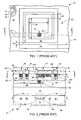
- FIG. 1 PRIOR ART
- a substrate 12 of a material such as silicon, has a plurality of dielectric layers formed thereon of a material such as silicon dioxide.
- a field dielectric layer 14 such as a field oxide
- a connecting interlayer dielectric (ILD) layer 16 such as a silicon oxide
- a first level ILD layer 18, and a second level ILD layer 20 are formed over the substrate 12.
- a spiral stacked inductor 22 Embedded within the dielectric layers.
- over as used in herein is defined vertically above a horizontal plane parallel to the conventional surface of a wafer on which the on-chip inductor is formed regardless of the orientation of the wafer. Terms, such as “on”, “below”, “higher”, “lower”, “above”, and “under”, are defined with respect to the horizontal plane.
- processed or “forming” as used herein to refer to the formation of vias and turns includes conventional semiconductor deposition of photoresist, hard and soft mask photolithography, etch, and strip, as appropriate.
- the spiral stacked inductor 22 is a two-turn stacked inductor.
- FIG. 1 PRIOR ART
- first and second turns 24 and 26 are shown.
- a first connecting portion 30 having connecting vias 32 connects to the spiral stacked inductor 22 at one end and a second connecting portion 34 connects at the other end.
- the first turn 24 has an inner diameter 36, a width 38 which is common to each of the turns, and a spacing 40 between each of the turns.
- the first connecting portion 30 passes under the two turns and thus is also referred to as an underpass 30.
- FIG. 2 PRIOR ART
- the substrate 12 has the field dielectric layer 14 upon which a conductive material is deposited and patterned to form the underpass 30.
- the connecting ILD layer 16 is then deposited over the underpass 30.
- One or more first via openings are formed in the connecting ILD layer 16 connected to the underpass 30.
- a conductive material layer is deposited on the connecting ILD layer 16 and processed to form a first level of the spiral stacked inductor 22. When processed, first and second turns 24' and 26' of a first level 50' will be formed. The first via openings are also filled with conductive material to form the connecting vias 32.
- the first level ILD layer 18 is then deposited over the first level 50'.
- a conductive material is deposited on the first level ILD layer 18 and processed to form the first and second turns 24 and 26 of a second level 50'.
- the first and second turns 24 and 26 are respectively connected to the first and second turn vias 24v and 26v along their lengths by the conductive material filling the respective vias openings to form first and second turn vias 24v and 26v.
- the second level ILD layer 20 is then deposited over the second level 50'.
- the passage of current (direction indicated by double circles as being an arrow head and the x in a circle being the tail) through the spiral stacked inductor 22 causes the creation of magnetic fields 52 which induce magnetic fields 54 in the substrate 12.
- an eddy current 56 is induced in the low resistivity substrate 12, which flows in a direction that is opposite to the flow in the spiral stacked inductor 22. This causes a magnetic loss that results in the degradation of the overall useful inductance of the spiral stacked inductor 22.
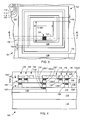
- a substrate 112 of a material such as silicon has a plurality of dielectric layers formed thereon of a material such as silicon dioxide.
- a field dielectric layer 114 such as a field oxide
- a connecting interlayer dielectric (ILD) layer 116 such as a silicon oxide
- a first level ILD layer 118, a second level ILD layer 120, and a third level ILD layer 121 are formed over the substrate 112.
- a 3-D spiral stacked inductor 122 Embedded within the dielectric layers.
- the 3-D spiral stacked inductor 122 is shown as being square spiral but it may also be circular spiral. Similarly, the 3-D spiral stacked inductor 122 can be a spiral, which is either clockwise or counter clockwise as viewed from above.
- the 3-D spiral stacked inductor 122 is a 3-D three-turn inductor.
- first, second, and third turns 124, 126, and 128 are shown.
- the turns can be flat as shown or circular, and can be made from any conductive material including copper.
- a first connecting portion 130 having connecting vias 132 connects to the 3-D spiral stacked inductor 122 at one end and a second connecting portion 134 connects at the other end to the third turn 128.
- the first turn 126 has an inner diameter 136, a width 138 which is common to each of the turns, and a spacing 140 between each of the turns.
- the first connecting portion 130 passes under the three turns and thus is also referred to as an underpass 130.
- FIG. 4 therein is shown a cross-sectional view of the 3-D spiral stacked inductor 100 of the present invention along line 4--4 of FIG. 3.
- the substrate 112 has the field dielectric 114 upon which a conductive material is deposited and patterned to form the underpass 130.
- the connecting ILD layer 116 is then deposited over the underpass 130.
- One or more first via openings are formed in the connecting ILD layer 116 connected to the under pass 130.
- a conductive material layer is deposited on the connecting ILD layer 116 and processed to form a first level of the spiral stacked inductor 122.
- a third turn 128' of a first level 150' will be formed and a first connecting contact 130' is formed at the first level 150'.
- the first via openings are filled with conductive material to form the connecting vias 132.
- the first level ILD layer 118 is then deposited over the first level 150'.
- One or more second via openings are formed in the first level ILD layer 118 connected to the third turn 128' and the first connecting contact 130'. The second via openings extend substantially along the entire length of the third turn 128'.
- a conductive material is deposited on the first level ILD layer 118 and processed to form second and third turns 126" and 128" and a second connecting contact 130" of a second level 150".
- the third turn 128" is connected to the third turn 128' along its length by the conductive material filling the second via openings to form first level third turn vias 128v1.
- the second connecting contact 130" is connected to the first connecting contact 130' by conductive material filling the second via openings to form first connecting vias 132v1.
- the second level ILD layer 120 is then deposited over the second level 150".
- One or more third via openings are formed in the second ILD layer 120 connected to the second and third turns 126" and 128", and the second connecting contact 130".
- the third via openings extend substantially along the entire length of the second and third turns 126" and 128".
- a conductive material is deposited on the second level ILD layer 120 and processed to form first, second, and third turns 124, 126, and 128 of a third level 150"'.
- the first, second, and third turns 124, 126, and 128 are respectively connected to the second connecting contact 130" by conductive material filling the third via openings to form second connecting vias 132v2, and the second level second and third turns 126" and 128" by conductive material filling the third via openings to form second level second and third turn vias 126v2 and 128v2.
- the third level ILD layer 121 is then deposited over the third level 150"'.
- spiral stacked inductor 22 As will be understood by those skilled in the art, as the spiral stacked inductor 22 has more turns, it will still have the same number of turns in each level and the turns will all be connected by pluralities of vias. On the other hand, as the 3-D spiral stacked inductor 122 has more turns, it has more levels with a fewer number of turns per level and, although the turns will all be connected by pluralities of vias, a lower number of turns at the lowest levels.
- a 3-D two turn inductor has two levels having one turn in a first level and two turns in a second level; a 3-D three turn inductor is shown; a 3-D four turn inductor has four levels with one turn in a first level, two turns in a second level, three turns in a third level, and four turns in a fourth level; etc.
- 3-D spiral stacked inductors could be made in the same fashion as shown with various configurations (such as circular), diameters, widths, and spacings.
- different metals can be used for the inductors including aluminum and copper.
Landscapes
- Engineering & Computer Science (AREA)
- Power Engineering (AREA)
- Computer Hardware Design (AREA)
- Microelectronics & Electronic Packaging (AREA)
- Physics & Mathematics (AREA)
- Condensed Matter Physics & Semiconductors (AREA)
- General Physics & Mathematics (AREA)
- Coils Or Transformers For Communication (AREA)
- Semiconductor Integrated Circuits (AREA)
- Manufacturing Cores, Coils, And Magnets (AREA)
- Resistance Heating (AREA)
Applications Claiming Priority (2)
| Application Number | Priority Date | Filing Date | Title |
|---|---|---|---|
| US131336 | 1993-10-04 | ||
| US10/131,336 US6841847B2 (en) | 2002-09-04 | 2002-09-04 | 3-D spiral stacked inductor on semiconductor material |
Publications (3)
| Publication Number | Publication Date |
|---|---|
| EP1396875A2 true EP1396875A2 (fr) | 2004-03-10 |
| EP1396875A3 EP1396875A3 (fr) | 2006-06-07 |
| EP1396875B1 EP1396875B1 (fr) | 2008-11-19 |
Family
ID=31713985
Family Applications (1)
| Application Number | Title | Priority Date | Filing Date |
|---|---|---|---|
| EP03019916A Expired - Lifetime EP1396875B1 (fr) | 2002-09-04 | 2003-09-02 | Inducteur en spirale 3-D empilé sur un substrat semiconducteur |
Country Status (6)
| Country | Link |
|---|---|
| US (2) | US6841847B2 (fr) |
| EP (1) | EP1396875B1 (fr) |
| JP (1) | JP4505201B2 (fr) |
| AT (1) | ATE414990T1 (fr) |
| DE (1) | DE60324748D1 (fr) |
| SG (2) | SG151088A1 (fr) |
Families Citing this family (41)
| Publication number | Priority date | Publication date | Assignee | Title |
|---|---|---|---|---|
| US20050104158A1 (en) * | 2003-11-19 | 2005-05-19 | Scintera Networks, Inc. | Compact, high q inductor for integrated circuit |
| US7283029B2 (en) * | 2004-12-08 | 2007-10-16 | Purdue Research Foundation | 3-D transformer for high-frequency applications |
| US7221251B2 (en) * | 2005-03-22 | 2007-05-22 | Acutechnology Semiconductor | Air core inductive element on printed circuit board for use in switching power conversion circuitries |
| US7399696B2 (en) * | 2005-08-02 | 2008-07-15 | International Business Machines Corporation | Method for high performance inductor fabrication using a triple damascene process with copper BEOL |
| TWI299556B (en) * | 2006-07-07 | 2008-08-01 | Holtek Semiconductor Inc | Spiral inductor with high quality factor of integrated circuit |
| CN101090025B (zh) * | 2007-05-25 | 2012-10-03 | 威盛电子股份有限公司 | 一种具有多层结构的螺旋电感元件 |
| JP5578797B2 (ja) | 2009-03-13 | 2014-08-27 | ルネサスエレクトロニクス株式会社 | 半導体装置 |
| TWI385680B (zh) * | 2009-05-19 | 2013-02-11 | Realtek Semiconductor Corp | 螺旋電感之堆疊結構 |
| US8143952B2 (en) | 2009-10-08 | 2012-03-27 | Qualcomm Incorporated | Three dimensional inductor and transformer |
| US8319564B2 (en) * | 2010-03-26 | 2012-11-27 | Altera Corporation | Integrated circuits with configurable inductors |
| US8692608B2 (en) | 2011-09-19 | 2014-04-08 | United Microelectronics Corp. | Charge pump system capable of stabilizing an output voltage |
| US9030221B2 (en) | 2011-09-20 | 2015-05-12 | United Microelectronics Corporation | Circuit structure of test-key and test method thereof |
| US8395455B1 (en) | 2011-10-14 | 2013-03-12 | United Microelectronics Corp. | Ring oscillator |
| US8421509B1 (en) | 2011-10-25 | 2013-04-16 | United Microelectronics Corp. | Charge pump circuit with low clock feed-through |
| US8588020B2 (en) | 2011-11-16 | 2013-11-19 | United Microelectronics Corporation | Sense amplifier and method for determining values of voltages on bit-line pair |
| CN102522388B (zh) * | 2011-12-22 | 2015-11-11 | 上海华虹宏力半导体制造有限公司 | 电感及形成方法 |
| US8493806B1 (en) | 2012-01-03 | 2013-07-23 | United Microelectronics Corporation | Sense-amplifier circuit of memory and calibrating method thereof |
| US8970197B2 (en) | 2012-08-03 | 2015-03-03 | United Microelectronics Corporation | Voltage regulating circuit configured to have output voltage thereof modulated digitally |
| US8724404B2 (en) | 2012-10-15 | 2014-05-13 | United Microelectronics Corp. | Memory, supply voltage generation circuit, and operation method of a supply voltage generation circuit used for a memory array |
| US8836460B2 (en) * | 2012-10-18 | 2014-09-16 | International Business Machines Corporation | Folded conical inductor |
| US8669897B1 (en) | 2012-11-05 | 2014-03-11 | United Microelectronics Corp. | Asynchronous successive approximation register analog-to-digital converter and operating method thereof |
| US8711598B1 (en) | 2012-11-21 | 2014-04-29 | United Microelectronics Corp. | Memory cell and memory cell array using the same |
| US8873295B2 (en) | 2012-11-27 | 2014-10-28 | United Microelectronics Corporation | Memory and operation method thereof |
| US8643521B1 (en) | 2012-11-28 | 2014-02-04 | United Microelectronics Corp. | Digital-to-analog converter with greater output resistance |
| US8953401B2 (en) | 2012-12-07 | 2015-02-10 | United Microelectronics Corp. | Memory device and method for driving memory array thereof |
| US9030886B2 (en) | 2012-12-07 | 2015-05-12 | United Microelectronics Corp. | Memory device and driving method thereof |
| US8917109B2 (en) | 2013-04-03 | 2014-12-23 | United Microelectronics Corporation | Method and device for pulse width estimation |
| US9105355B2 (en) | 2013-07-04 | 2015-08-11 | United Microelectronics Corporation | Memory cell array operated with multiple operation voltage |
| US9831026B2 (en) * | 2013-07-24 | 2017-11-28 | Globalfoundries Inc. | High efficiency on-chip 3D transformer structure |
| US9251948B2 (en) | 2013-07-24 | 2016-02-02 | International Business Machines Corporation | High efficiency on-chip 3D transformer structure |
| US9779869B2 (en) | 2013-07-25 | 2017-10-03 | International Business Machines Corporation | High efficiency on-chip 3D transformer structure |
| US9171663B2 (en) | 2013-07-25 | 2015-10-27 | Globalfoundries U.S. 2 Llc | High efficiency on-chip 3D transformer structure |
| US8947911B1 (en) | 2013-11-07 | 2015-02-03 | United Microelectronics Corp. | Method and circuit for optimizing bit line power consumption |
| US8866536B1 (en) | 2013-11-14 | 2014-10-21 | United Microelectronics Corp. | Process monitoring circuit and method |
| US9143143B2 (en) | 2014-01-13 | 2015-09-22 | United Microelectronics Corp. | VCO restart up circuit and method thereof |
| KR20160058592A (ko) * | 2014-11-17 | 2016-05-25 | 에스케이하이닉스 주식회사 | 알에프 집적회로 및 그 제조방법 |
| US9653204B2 (en) | 2015-01-22 | 2017-05-16 | Globalfoundries Inc. | Symmetric multi-port inductor for differential multi-band RF circuits |
| US10249580B2 (en) * | 2016-06-22 | 2019-04-02 | Qualcomm Incorporated | Stacked substrate inductor |
| US10525690B2 (en) | 2016-09-07 | 2020-01-07 | General Electric Company | Additive manufacturing-based low-profile inductor |
| US10199157B2 (en) | 2016-09-30 | 2019-02-05 | Intel IP Corporation | Stacked metal inductor |
| TWI723343B (zh) * | 2019-02-19 | 2021-04-01 | 頎邦科技股份有限公司 | 具立體電感之半導體結構及其製造方法 |
Citations (3)
| Publication number | Priority date | Publication date | Assignee | Title |
|---|---|---|---|---|
| US5446311A (en) * | 1994-09-16 | 1995-08-29 | International Business Machines Corporation | High-Q inductors in silicon technology without expensive metalization |
| US5831331A (en) * | 1996-11-22 | 1998-11-03 | Philips Electronics North America Corporation | Self-shielding inductor for multi-layer semiconductor integrated circuits |
| US20020067236A1 (en) * | 1998-12-11 | 2002-06-06 | Toshiakira Andoh | High-Q inductor for high frequency |
Family Cites Families (12)
| Publication number | Priority date | Publication date | Assignee | Title |
|---|---|---|---|---|
| JP2938631B2 (ja) * | 1991-08-28 | 1999-08-23 | 太陽誘電株式会社 | 積層セラミックインダクタの製造方法 |
| JPH06163270A (ja) * | 1992-11-19 | 1994-06-10 | Murata Mfg Co Ltd | 多層基板 |
| JPH07106514A (ja) * | 1993-10-07 | 1995-04-21 | Toshiba Corp | 半導体集積回路装置 |
| JP2904086B2 (ja) * | 1995-12-27 | 1999-06-14 | 日本電気株式会社 | 半導体装置およびその製造方法 |
| JP3164025B2 (ja) * | 1997-08-04 | 2001-05-08 | 日本電気株式会社 | 半導体集積回路装置及びその製造方法 |
| KR100279753B1 (ko) * | 1997-12-03 | 2001-03-02 | 정선종 | 반도체 집적회로 제조공정을 이용한 인덕터 제조방법 |
| JPH11224825A (ja) * | 1998-02-06 | 1999-08-17 | Murata Mfg Co Ltd | 電子部品の製造方法 |
| US6426267B2 (en) * | 1998-06-19 | 2002-07-30 | Winbond Electronics Corp. | Method for fabricating high-Q inductance device in monolithic technology |
| US6472285B1 (en) * | 1999-04-30 | 2002-10-29 | Winbond Electronics Corporation | Method for fabricating high-Q inductance device in monolithic technology |
| US6054914A (en) * | 1998-07-06 | 2000-04-25 | Midcom, Inc. | Multi-layer transformer having electrical connection in a magnetic core |
| TW386279B (en) * | 1998-08-07 | 2000-04-01 | Winbond Electronics Corp | Inductor structure with air gap and method of manufacturing thereof |
| JP2002246231A (ja) * | 2001-02-14 | 2002-08-30 | Murata Mfg Co Ltd | 積層型インダクタ |
-
2002
- 2002-09-04 US US10/131,336 patent/US6841847B2/en not_active Expired - Lifetime
-
2003
- 2003-09-02 EP EP03019916A patent/EP1396875B1/fr not_active Expired - Lifetime
- 2003-09-02 SG SG200505168-5A patent/SG151088A1/en unknown
- 2003-09-02 AT AT03019916T patent/ATE414990T1/de not_active IP Right Cessation
- 2003-09-02 SG SG200305645A patent/SG109527A1/en unknown
- 2003-09-02 DE DE60324748T patent/DE60324748D1/de not_active Expired - Lifetime
- 2003-09-04 JP JP2003312890A patent/JP4505201B2/ja not_active Expired - Fee Related
-
2004
- 2004-10-08 US US10/962,007 patent/US7721414B2/en not_active Expired - Fee Related
Patent Citations (3)
| Publication number | Priority date | Publication date | Assignee | Title |
|---|---|---|---|---|
| US5446311A (en) * | 1994-09-16 | 1995-08-29 | International Business Machines Corporation | High-Q inductors in silicon technology without expensive metalization |
| US5831331A (en) * | 1996-11-22 | 1998-11-03 | Philips Electronics North America Corporation | Self-shielding inductor for multi-layer semiconductor integrated circuits |
| US20020067236A1 (en) * | 1998-12-11 | 2002-06-06 | Toshiakira Andoh | High-Q inductor for high frequency |
Also Published As
| Publication number | Publication date |
|---|---|
| SG109527A1 (en) | 2005-03-30 |
| ATE414990T1 (de) | 2008-12-15 |
| EP1396875A3 (fr) | 2006-06-07 |
| EP1396875B1 (fr) | 2008-11-19 |
| JP2004104129A (ja) | 2004-04-02 |
| US20040041234A1 (en) | 2004-03-04 |
| US7721414B2 (en) | 2010-05-25 |
| JP4505201B2 (ja) | 2010-07-21 |
| SG151088A1 (en) | 2009-04-30 |
| US6841847B2 (en) | 2005-01-11 |
| US20050057335A1 (en) | 2005-03-17 |
| DE60324748D1 (de) | 2009-01-02 |
Similar Documents
| Publication | Publication Date | Title |
|---|---|---|
| EP1396875B1 (fr) | Inducteur en spirale 3-D empilé sur un substrat semiconducteur | |
| US6750750B2 (en) | Via/line inductor on semiconductor material | |
| US20180175136A1 (en) | Inductor element, inductor element manufacturing method, and semiconductor device with inductor element mounted thereon | |
| US7808358B2 (en) | Inductor and method for fabricating the same | |
| US7436281B2 (en) | Method to improve inductance with a high-permeability slotted plate core in an integrated circuit | |
| US7381607B2 (en) | Method of forming a spiral inductor in a semiconductor substrate | |
| US7977767B2 (en) | Spiral planar inductor and manufacturing method thereof | |
| US6281778B1 (en) | Monolithic inductor with magnetic flux lines guided away from substrate | |
| US6650220B2 (en) | Parallel spiral stacked inductor on semiconductor material | |
| US20070126543A1 (en) | Integrated inductor | |
| US6714112B2 (en) | Silicon-based inductor with varying metal-to-metal conductor spacing | |
| US7978043B2 (en) | Semiconductor device | |
| WO2009101565A1 (fr) | Topologie optimisée pour bobine d'inductance à faible champ magnétique parasite | |
| JP2002009166A (ja) | 集積された誘導性回路 | |
| US7262481B1 (en) | Fill structures for use with a semiconductor integrated circuit inductor | |
| KR20030029492A (ko) | 반도체 기판에 형성되는 박막 다층 하이 q 변압기 | |
| JP2006066769A (ja) | インダクタ及びその製造方法 | |
| JP2010114283A (ja) | スパイラルインダクタ | |
| JP2006108323A (ja) | インダクタンス素子及びその製造方法 | |
| US20090283855A1 (en) | Semiconductor device and process for manufacturing the same | |
| KR100821618B1 (ko) | 반도체 집적 회로에서 형성되는 인덕터 |
Legal Events
| Date | Code | Title | Description |
|---|---|---|---|
| PUAI | Public reference made under article 153(3) epc to a published international application that has entered the european phase |
Free format text: ORIGINAL CODE: 0009012 |
|
| AK | Designated contracting states |
Kind code of ref document: A2 Designated state(s): AT BE BG CH CY CZ DE DK EE ES FI FR GB GR HU IE IT LI LU MC NL PT RO SE SI SK TR |
|
| AX | Request for extension of the european patent |
Extension state: AL LT LV MK |
|
| RIN1 | Information on inventor provided before grant (corrected) |
Inventor name: CHEW, KOK WAI Inventor name: YEO, KIAT SENG Inventor name: CHU, SHAO-FU SANDFORD Inventor name: NG, CHENG YEOW Inventor name: SIA, CHOON-BENG Inventor name: GOH, WANG LING |
|
| PUAL | Search report despatched |
Free format text: ORIGINAL CODE: 0009013 |
|
| AK | Designated contracting states |
Kind code of ref document: A3 Designated state(s): AT BE BG CH CY CZ DE DK EE ES FI FR GB GR HU IE IT LI LU MC NL PT RO SE SI SK TR |
|
| AX | Request for extension of the european patent |
Extension state: AL LT LV MK |
|
| 17P | Request for examination filed |
Effective date: 20061204 |
|
| 17Q | First examination report despatched |
Effective date: 20070115 |
|
| AKX | Designation fees paid |
Designated state(s): AT BE BG CH CY CZ DE DK EE ES FI FR GB GR HU IE IT LI LU MC NL PT RO SE SI SK TR |
|
| GRAP | Despatch of communication of intention to grant a patent |
Free format text: ORIGINAL CODE: EPIDOSNIGR1 |
|
| RIC1 | Information provided on ipc code assigned before grant |
Ipc: H01L 27/08 20060101ALI20080514BHEP Ipc: H01L 21/02 20060101AFI20080514BHEP |
|
| GRAS | Grant fee paid |
Free format text: ORIGINAL CODE: EPIDOSNIGR3 |
|
| GRAA | (expected) grant |
Free format text: ORIGINAL CODE: 0009210 |
|
| AK | Designated contracting states |
Kind code of ref document: B1 Designated state(s): AT BE BG CH CY CZ DE DK EE ES FI FR GB GR HU IE IT LI LU MC NL PT RO SE SI SK TR |
|
| REG | Reference to a national code |
Ref country code: GB Ref legal event code: FG4D |
|
| REG | Reference to a national code |
Ref country code: CH Ref legal event code: EP |
|
| REG | Reference to a national code |
Ref country code: IE Ref legal event code: FG4D |
|
| REF | Corresponds to: |
Ref document number: 60324748 Country of ref document: DE Date of ref document: 20090102 Kind code of ref document: P |
|
| PG25 | Lapsed in a contracting state [announced via postgrant information from national office to epo] |
Ref country code: ES Free format text: LAPSE BECAUSE OF FAILURE TO SUBMIT A TRANSLATION OF THE DESCRIPTION OR TO PAY THE FEE WITHIN THE PRESCRIBED TIME-LIMIT Effective date: 20090301 Ref country code: AT Free format text: LAPSE BECAUSE OF FAILURE TO SUBMIT A TRANSLATION OF THE DESCRIPTION OR TO PAY THE FEE WITHIN THE PRESCRIBED TIME-LIMIT Effective date: 20081119 |
|
| NLV1 | Nl: lapsed or annulled due to failure to fulfill the requirements of art. 29p and 29m of the patents act | ||
| PG25 | Lapsed in a contracting state [announced via postgrant information from national office to epo] |
Ref country code: NL Free format text: LAPSE BECAUSE OF FAILURE TO SUBMIT A TRANSLATION OF THE DESCRIPTION OR TO PAY THE FEE WITHIN THE PRESCRIBED TIME-LIMIT Effective date: 20081119 Ref country code: SI Free format text: LAPSE BECAUSE OF FAILURE TO SUBMIT A TRANSLATION OF THE DESCRIPTION OR TO PAY THE FEE WITHIN THE PRESCRIBED TIME-LIMIT Effective date: 20081119 Ref country code: FI Free format text: LAPSE BECAUSE OF FAILURE TO SUBMIT A TRANSLATION OF THE DESCRIPTION OR TO PAY THE FEE WITHIN THE PRESCRIBED TIME-LIMIT Effective date: 20081119 |
|
| PG25 | Lapsed in a contracting state [announced via postgrant information from national office to epo] |
Ref country code: BE Free format text: LAPSE BECAUSE OF FAILURE TO SUBMIT A TRANSLATION OF THE DESCRIPTION OR TO PAY THE FEE WITHIN THE PRESCRIBED TIME-LIMIT Effective date: 20081119 Ref country code: BG Free format text: LAPSE BECAUSE OF FAILURE TO SUBMIT A TRANSLATION OF THE DESCRIPTION OR TO PAY THE FEE WITHIN THE PRESCRIBED TIME-LIMIT Effective date: 20090219 Ref country code: RO Free format text: LAPSE BECAUSE OF FAILURE TO SUBMIT A TRANSLATION OF THE DESCRIPTION OR TO PAY THE FEE WITHIN THE PRESCRIBED TIME-LIMIT Effective date: 20081119 Ref country code: EE Free format text: LAPSE BECAUSE OF FAILURE TO SUBMIT A TRANSLATION OF THE DESCRIPTION OR TO PAY THE FEE WITHIN THE PRESCRIBED TIME-LIMIT Effective date: 20081119 Ref country code: DK Free format text: LAPSE BECAUSE OF FAILURE TO SUBMIT A TRANSLATION OF THE DESCRIPTION OR TO PAY THE FEE WITHIN THE PRESCRIBED TIME-LIMIT Effective date: 20081119 |
|
| PG25 | Lapsed in a contracting state [announced via postgrant information from national office to epo] |
Ref country code: SE Free format text: LAPSE BECAUSE OF FAILURE TO SUBMIT A TRANSLATION OF THE DESCRIPTION OR TO PAY THE FEE WITHIN THE PRESCRIBED TIME-LIMIT Effective date: 20090219 Ref country code: CZ Free format text: LAPSE BECAUSE OF FAILURE TO SUBMIT A TRANSLATION OF THE DESCRIPTION OR TO PAY THE FEE WITHIN THE PRESCRIBED TIME-LIMIT Effective date: 20081119 Ref country code: PT Free format text: LAPSE BECAUSE OF FAILURE TO SUBMIT A TRANSLATION OF THE DESCRIPTION OR TO PAY THE FEE WITHIN THE PRESCRIBED TIME-LIMIT Effective date: 20090420 |
|
| PLBE | No opposition filed within time limit |
Free format text: ORIGINAL CODE: 0009261 |
|
| STAA | Information on the status of an ep patent application or granted ep patent |
Free format text: STATUS: NO OPPOSITION FILED WITHIN TIME LIMIT |
|
| PG25 | Lapsed in a contracting state [announced via postgrant information from national office to epo] |
Ref country code: SK Free format text: LAPSE BECAUSE OF FAILURE TO SUBMIT A TRANSLATION OF THE DESCRIPTION OR TO PAY THE FEE WITHIN THE PRESCRIBED TIME-LIMIT Effective date: 20081119 |
|
| 26N | No opposition filed |
Effective date: 20090820 |
|
| PG25 | Lapsed in a contracting state [announced via postgrant information from national office to epo] |
Ref country code: MC Free format text: LAPSE BECAUSE OF NON-PAYMENT OF DUE FEES Effective date: 20090930 |
|
| REG | Reference to a national code |
Ref country code: CH Ref legal event code: PL |
|
| GBPC | Gb: european patent ceased through non-payment of renewal fee |
Effective date: 20090902 |
|
| PG25 | Lapsed in a contracting state [announced via postgrant information from national office to epo] |
Ref country code: IE Free format text: LAPSE BECAUSE OF NON-PAYMENT OF DUE FEES Effective date: 20090902 |
|
| PG25 | Lapsed in a contracting state [announced via postgrant information from national office to epo] |
Ref country code: GR Free format text: LAPSE BECAUSE OF FAILURE TO SUBMIT A TRANSLATION OF THE DESCRIPTION OR TO PAY THE FEE WITHIN THE PRESCRIBED TIME-LIMIT Effective date: 20090220 Ref country code: CH Free format text: LAPSE BECAUSE OF NON-PAYMENT OF DUE FEES Effective date: 20090930 Ref country code: LI Free format text: LAPSE BECAUSE OF NON-PAYMENT OF DUE FEES Effective date: 20090930 |
|
| PG25 | Lapsed in a contracting state [announced via postgrant information from national office to epo] |
Ref country code: GB Free format text: LAPSE BECAUSE OF NON-PAYMENT OF DUE FEES Effective date: 20090902 |
|
| PG25 | Lapsed in a contracting state [announced via postgrant information from national office to epo] |
Ref country code: LU Free format text: LAPSE BECAUSE OF NON-PAYMENT OF DUE FEES Effective date: 20090902 |
|
| PG25 | Lapsed in a contracting state [announced via postgrant information from national office to epo] |
Ref country code: HU Free format text: LAPSE BECAUSE OF FAILURE TO SUBMIT A TRANSLATION OF THE DESCRIPTION OR TO PAY THE FEE WITHIN THE PRESCRIBED TIME-LIMIT Effective date: 20090520 |
|
| PG25 | Lapsed in a contracting state [announced via postgrant information from national office to epo] |
Ref country code: TR Free format text: LAPSE BECAUSE OF FAILURE TO SUBMIT A TRANSLATION OF THE DESCRIPTION OR TO PAY THE FEE WITHIN THE PRESCRIBED TIME-LIMIT Effective date: 20081119 |
|
| PG25 | Lapsed in a contracting state [announced via postgrant information from national office to epo] |
Ref country code: CY Free format text: LAPSE BECAUSE OF FAILURE TO SUBMIT A TRANSLATION OF THE DESCRIPTION OR TO PAY THE FEE WITHIN THE PRESCRIBED TIME-LIMIT Effective date: 20081119 |
|
| PGFP | Annual fee paid to national office [announced via postgrant information from national office to epo] |
Ref country code: FR Payment date: 20110922 Year of fee payment: 9 |
|
| PGFP | Annual fee paid to national office [announced via postgrant information from national office to epo] |
Ref country code: IT Payment date: 20110914 Year of fee payment: 9 |
|
| REG | Reference to a national code |
Ref country code: FR Ref legal event code: ST Effective date: 20130531 |
|
| PG25 | Lapsed in a contracting state [announced via postgrant information from national office to epo] |
Ref country code: FR Free format text: LAPSE BECAUSE OF NON-PAYMENT OF DUE FEES Effective date: 20121001 Ref country code: IT Free format text: LAPSE BECAUSE OF NON-PAYMENT OF DUE FEES Effective date: 20120902 |
|
| PGFP | Annual fee paid to national office [announced via postgrant information from national office to epo] |
Ref country code: DE Payment date: 20210720 Year of fee payment: 19 |
|
| REG | Reference to a national code |
Ref country code: DE Ref legal event code: R119 Ref document number: 60324748 Country of ref document: DE |
|
| PG25 | Lapsed in a contracting state [announced via postgrant information from national office to epo] |
Ref country code: DE Free format text: LAPSE BECAUSE OF NON-PAYMENT OF DUE FEES Effective date: 20230401 |